ICGOO在线商城 > 集成电路(IC) > PMIC - 稳压器 - 线性 > UC285T-ADJ
 Datasheet下载
- 型号: UC285T-ADJ
- 制造商: Texas Instruments
- 库位|库存: xxxx|xxxx
- 要求:
| 数量阶梯 | 香港交货 | 国内含税 |
| +xxxx | $xxxx | ¥xxxx |
查看当月历史价格
查看今年历史价格
UC285T-ADJ产品简介:
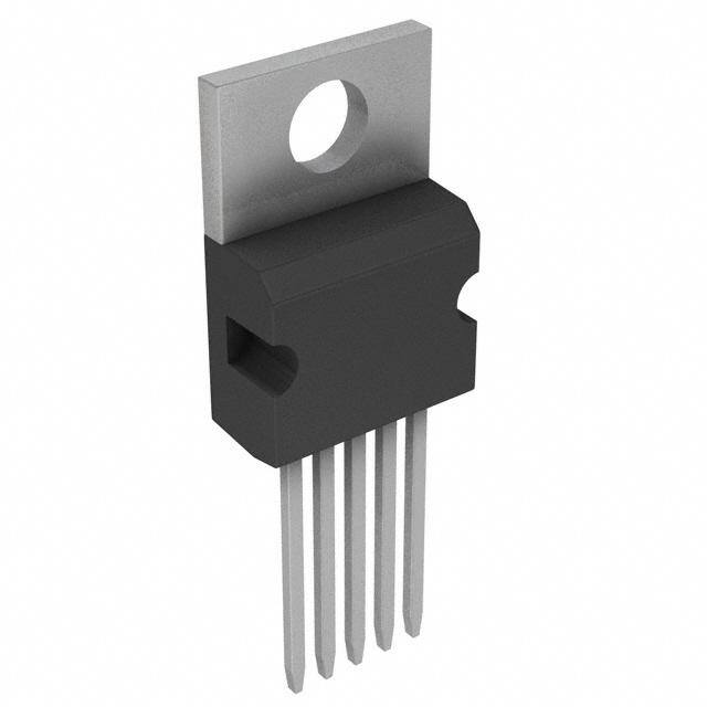
ICGOO电子元器件商城为您提供UC285T-ADJ由Texas Instruments设计生产,在icgoo商城现货销售,并且可以通过原厂、代理商等渠道进行代购。 UC285T-ADJ价格参考¥37.88-¥70.35。Texas InstrumentsUC285T-ADJ封装/规格:PMIC - 稳压器 - 线性, Linear Voltage Regulator IC Positive Fixed or Adjustable 1 Output 1.2V, 1.22 V ~ 6 V 5A TO-220-5。您可以下载UC285T-ADJ参考资料、Datasheet数据手册功能说明书,资料中有UC285T-ADJ 详细功能的应用电路图电压和使用方法及教程。
UC285T-ADJ 是由 Texas Instruments(德州仪器)生产的一款线性稳压器,属于 PMIC(电源管理集成电路)类别。该型号具有可调输出电压功能,适用于多种需要稳定直流电源的场景。以下是其主要应用场景:

1. 便携式电子设备
   UC285T-ADJ 的低功耗特性和小型封装使其非常适合用于便携式设备,例如手持终端、无线耳机、电子阅读器和便携式医疗设备等。这些设备通常对电源效率和稳定性要求较高,而线性稳压器能够提供干净的电源输出。

2. 嵌入式系统
   在工业控制、物联网设备和其他嵌入式系统中,UC285T-ADJ 可以为微控制器、传感器和其他低功耗组件提供稳定的电源支持。其可调输出特性允许根据具体需求灵活设置电压。

3. 通信设备
   该稳压器可用于通信领域的低功耗模块,例如无线模块、蓝牙模块和 Zigbee 模块。它能够为射频电路和信号处理单元提供精确的供电,确保通信质量。

4. 消费类电子产品
   在家用电器和消费类电子产品中,如遥控器、智能家居设备和小型音响系统,UC285T-ADJ 能够提供高效且稳定的电源解决方案。

5. 汽车电子
   虽然 UC285T-ADJ 主要针对低功耗应用,但在某些非关键车载子系统中(如车内照明、娱乐系统或传感器模块),它也可以作为电源管理的一部分使用。

6. 电池供电设备
   对于依赖电池供电的设备,UC285T-ADJ 的高效能和可调输出特性可以帮助延长电池寿命,同时确保设备运行在最佳电压范围内。

总之,UC285T-ADJ 凭借其灵活性和可靠性,广泛应用于需要低噪声、高稳定性和可调节输出电压的各种场景中。它的简单设计和易于使用的特性也使其成为工程师在开发低功耗产品时的理想选择。
| 参数 | 数值 |
| 产品目录 | 集成电路 (IC)半导体 |
| 描述 | IC REG LDO 1.2V/ADJ 5A TO220-5低压差稳压器 Fast Transient Resp 5 Amp LDO |
| 产品分类 | |
| 品牌 | Texas Instruments |
| 产品手册 | |
| 产品图片 |
|
| rohs | 符合RoHS无铅 / 符合限制有害物质指令(RoHS)规范要求 |
| 产品系列 | 电源管理 IC,低压差稳压器,Texas Instruments UC285T-ADJ- |
| 数据手册 | |
| 产品型号 | UC285T-ADJ |
| 产品目录页面 | |
| 产品种类 | 低压差稳压器 |
| 供应商器件封装 | TO-220-5 |
| 其它名称 | 296-15156-5 |
| 包装 | 管件 |
| 单位重量 | 2 g |
| 商标 | Texas Instruments |
| 回动电压—最大值 | 425 mV at 5 A |
| 安装类型 | 通孔 |
| 安装风格 | Through Hole |
| 封装 | Tube |
| 封装/外壳 | TO-220-5 |
| 封装/箱体 | TO-220-5 |
| 工作温度 | -40°C ~ 100°C |
| 工厂包装数量 | 50 |
| 最大工作温度 | + 100 C |
| 最大输入电压 | 7.5 V |
| 最小工作温度 | - 40 C |
| 最小输入电压 | + 1.7 V |
| 标准包装 | 50 |
| 电压-跌落(典型值) | - |
| 电压-输入 | 1.7 V ~ 7.5 V |
| 电压-输出 | 1.2V,1.22 V ~ 6 V |
| 电流-输出 | 5A |
| 电流-限制(最小值) | 5.1A |
| 稳压器拓扑 | 正,固定式或可调式 |
| 稳压器数 | 1 |
| 系列 | UC285-ADJ |
| 负载调节 | 4 mV |
| 输入偏压电流—最大 | 8 mA |
| 输出电压 | 6 V, 1.2 V |
| 输出电流 | 5 A |
| 输出端数量 | 1 Output |
| 输出类型 | Adjustable |

_4040208^C.jpg)


- 商务部:美国ITC正式对集成电路等产品启动337调查
- 曝三星4nm工艺存在良率问题 高通将骁龙8 Gen1或转产台积电
- 太阳诱电将投资9.5亿元在常州建新厂生产MLCC 预计2023年完工
- 英特尔发布欧洲新工厂建设计划 深化IDM 2.0 战略
- 台积电先进制程称霸业界 有大客户加持明年业绩稳了
- 达到5530亿美元!SIA预计今年全球半导体销售额将创下新高
- 英特尔拟将自动驾驶子公司Mobileye上市 估值或超500亿美元
- 三星加码芯片和SET,合并消费电子和移动部门,撤换高东真等 CEO
- 三星电子宣布重大人事变动 还合并消费电子和移动部门
- 海关总署:前11个月进口集成电路产品价值2.52万亿元 增长14.8%


PDF Datasheet 数据手册内容提取
(cid:25) (cid:1)(cid:2)(cid:3)(cid:4)(cid:5)(cid:6)(cid:7)(cid:8) (cid:1)(cid:2)(cid:3)(cid:4)(cid:5)(cid:6)(cid:3)(cid:8) (cid:1)(cid:2)(cid:3)(cid:4)(cid:5)(cid:6)(cid:9)(cid:8) (cid:1)(cid:2)(cid:3)(cid:4)(cid:5)(cid:6)(cid:10)(cid:11)(cid:12)(cid:8) (cid:1)(cid:2)(cid:9)(cid:4)(cid:5)(cid:6)(cid:7)(cid:8) (cid:1)(cid:2)(cid:9)(cid:4)(cid:5)(cid:6)(cid:3)(cid:8) (cid:1)(cid:2)(cid:9)(cid:4)(cid:5)(cid:6)(cid:9)(cid:8) (cid:1)(cid:2)(cid:9)(cid:4)(cid:5)(cid:6)(cid:10)(cid:11)(cid:12) (cid:13)(cid:10)(cid:14)(cid:15) (cid:15)(cid:16)(cid:10)(cid:17)(cid:14)(cid:18)(cid:19)(cid:17)(cid:15) (cid:16)(cid:19)(cid:14)(cid:20)(cid:21)(cid:17)(cid:14)(cid:19) (cid:5)(cid:6)(cid:10) (cid:22)(cid:21)(cid:23)(cid:6)(cid:11)(cid:16)(cid:21)(cid:20)(cid:21)(cid:1)(cid:15) (cid:16)(cid:19)(cid:24)(cid:1)(cid:22)(cid:10)(cid:15)(cid:21)(cid:16) SLUS212E − NOVEMBER 1999 − REVISED FEBRUARY 2004 (cid:1) Fast Transient Response 5-PIN TO-220 (cid:1) T PACKAGE (TOP VIEW) 10-mA to 5-A Load Current (cid:1) Short Circuit Protection (cid:1) Maximum Dropout of 500-mV at 5-A Load Current (cid:1) Separate Bias (VB) and VIN Pins (cid:1) Available in Adjustable or Fixed Output Voltages (cid:1) 5-Pin Package Allows Kelvin Sensing of Load Voltage 5-PIN TO-263 (cid:1) TD PACKAGE Reverse Current Protection (TOP VIEW) Note: Tab = Ground description The UC385 is a low dropout linear regulator providing a quick response to fast load changes. Combined with its precision onboard reference, the UC385 excels at driving GTL and BTL buses. Due to its fast response to load transients, the total capacitance required to decouple the regulator’s output can be significantly decreased when compared to standard LDO linear regulators. Dropout voltage (VIN to VOUT) is only 490 mV maximum and 350 mV typical at 5-A load (0°C to 100°C). The onboard bandgap reference is stable with temperature and scaled for a 1.2 V input to the internal power amplifier. The UC385 is available in fixed output voltages of 1.5 V, 2.1 V, or 2.5 V. The output voltage of the adjustable version can be set with two external resistors. If the external resistors are omitted, the output voltage defaults to 1.2 V. block diagram VB 1 R1 R2 UC382−ADJ OPEN 0 UC382−1 (1.5 V) 2 kΩ 500Ω UC382−2 (2.1 V) 2 kΩ 1.5 kΩ UC382−3 (2.5 V) 2 kΩ 2.16 kΩ THERMAL SHUTDOWN 2 VIN 1.2 V BANDGAP + REFERENCE SHORT R1 R2 CIRCUIT SENSE 3 5 4 GND ADJ VOUT UDG-00084 Please be aware that an important notice concerning availability, standard warranty, and use in critical applications of TexasInstruments semiconductor products and disclaimers thereto appears at the end of this data sheet. All trademarks are the property of their respective owners. (cid:20)(cid:16)(cid:21)(cid:11)(cid:1)(cid:2)(cid:15)(cid:18)(cid:21)(cid:17) (cid:11)(cid:10)(cid:15)(cid:10) (cid:26)(cid:27)(cid:28)(cid:29)(cid:30)(cid:31)!"(cid:26)(cid:29)(cid:27) (cid:26)# $%(cid:30)(cid:30)&(cid:27)" !# (cid:29)(cid:28) ’%()(cid:26)$!"(cid:26)(cid:29)(cid:27) *!"&+ Copyright 1998−2004, Texas Instruments Incorporated (cid:20)(cid:30)(cid:29)*%$"# $(cid:29)(cid:27)(cid:28)(cid:29)(cid:30)(cid:31) "(cid:29) #’&$(cid:26)(cid:28)(cid:26)$!"(cid:26)(cid:29)(cid:27)# ’&(cid:30) ",& "&(cid:30)(cid:31)# (cid:29)(cid:28) (cid:15)&-!# (cid:18)(cid:27)#"(cid:30)%(cid:31)&(cid:27)"# #"!(cid:27)*!(cid:30)* .!(cid:30)(cid:30)!(cid:27)"/+ (cid:20)(cid:30)(cid:29)*%$"(cid:26)(cid:29)(cid:27) ’(cid:30)(cid:29)$&##(cid:26)(cid:27)0 *(cid:29)&# (cid:27)(cid:29)" (cid:27)&$&##!(cid:30)(cid:26))/ (cid:26)(cid:27)$)%*& "&#"(cid:26)(cid:27)0 (cid:29)(cid:28) !)) ’!(cid:30)!(cid:31)&"&(cid:30)#+ POST OFFICE BOX 655303 • DALLAS, TEXAS 75265 1
(cid:1)(cid:2)(cid:3)(cid:4)(cid:5)(cid:6)(cid:7)(cid:8) (cid:1)(cid:2)(cid:3)(cid:4)(cid:5)(cid:6)(cid:3)(cid:8) (cid:1)(cid:2)(cid:3)(cid:4)(cid:5)(cid:6)(cid:9)(cid:8) (cid:1)(cid:2)(cid:3)(cid:4)(cid:5)(cid:6)(cid:10)(cid:11)(cid:12)(cid:8) (cid:1)(cid:2)(cid:9)(cid:4)(cid:5)(cid:6)(cid:7)(cid:8) (cid:1)(cid:2)(cid:9)(cid:4)(cid:5)(cid:6)(cid:3)(cid:8) (cid:1)(cid:2)(cid:9)(cid:4)(cid:5)(cid:6)(cid:9)(cid:8) (cid:1)(cid:2)(cid:9)(cid:4)(cid:5)(cid:6)(cid:10)(cid:11)(cid:12) (cid:25) (cid:13)(cid:10)(cid:14)(cid:15) (cid:15)(cid:16)(cid:10)(cid:17)(cid:14)(cid:18)(cid:19)(cid:17)(cid:15) (cid:16)(cid:19)(cid:14)(cid:20)(cid:21)(cid:17)(cid:14)(cid:19) (cid:5)(cid:6)(cid:10) (cid:22)(cid:21)(cid:23)(cid:6)(cid:11)(cid:16)(cid:21)(cid:20)(cid:21)(cid:1)(cid:15) (cid:16)(cid:19)(cid:24)(cid:1)(cid:22)(cid:10)(cid:15)(cid:21)(cid:16) SLUS212E − NOVEMBER 1999 − REVISED FEBRUARY 2004 absolute maximum ratings over operating free-air temperature (unless otherwise noted)† VIN . . . . . . . . . . . . . . . . . . . . . . . . . . . . . . . . . . . . . . . . . . . . . . . . . . . . . . . . . . . . . . . . . . . . . . . . . . . . . . . . . . . . . 7.5 V Output voltage . . . . . . . . . . . . . . . . . . . . . . . . . . . . . . . . . . . . . . . . . . . . . . . . . . . . . . . . . . . . . . . . . . . . 1.2 V to −6.0 V Storage temperature . . . . . . . . . . . . . . . . . . . . . . . . . . . . . . . . . . . . . . . . . . . . . . . . . . . . . . . . . . . . . −65°C to 150°C Junction temperature . . . . . . . . . . . . . . . . . . . . . . . . . . . . . . . . . . . . . . . . . . . . . . . . . . . . . . . . . . . . . −55°C to 150°C Lead temperature (soldering, 10 seconds) . . . . . . . . . . . . . . . . . . . . . . . . . . . . . . . . . . . . . . . . . . . . . . . . . . 300°C †Stresses beyond those listed under “absolute maximum ratings” may cause permanent damage to the device. These are stress ratings only, and functional operation of the device at these or any other conditions beyond those indicated under “recommended operating conditions” is not implied. Exposure to absolute-maximum-rated conditions for extended periods may affect device reliability. AVAILABLE OPTIONS(1) PACKAGED DEVICES TO-220 (T) TO−263 (TD)(2) TTJJ OUTPUT VOLTAGE OUTPUT VOLTAGE 1.5 V 2.1 V 2.5 V 1.2 V or ADJ 1.5 V 2.1 V 2.5 V 1.2 V or ADJ –40°C to 100°C 285T-1 285T-2 285T-3 285T-ADJ 285TD-1 285TD-2 285TD-3 285TD-ADJ 0°C to 100°C 385T-1 385T-2 385T-3 385T-ADJ 385TD-1 385TD-2 385TD-3 385TD-ADJ 1. For more package and ordering information, see the Package Option Addendum located at the end of this data sheet. 2. For 50 piece reel, add KTTT (e.g., UC285TDKTTT−1); for 500 piece reel, add TR (e.g., UC285TDTR−1). electrical characteristics unless otherwise stated, these parameters apply for T = −40°C to 100°C A for the UC285-x series and 0°C to 100°C for the UC385-x, VB = 5 V; VIN = 3.3 V, VOUT = 2.5 V, T = T . A J PARAMETER TEST CONDITION MIN TYP MAX UNIT UC385-3 Fixed 2.5 V, 5-A Family OOuuttppuutt vvoollttaaggee UC385-3 IVOUT = 100 mA 2.475 2.5 2.525 V UC285-3 IVOUT = 100 mA 2.45 2.5 2.525 V Load regulation IVOUT = 10 mA to 5 A 0.5 4 mV VIN PSRR 80 110 dB VB PSRR 50 65 dB VVIINN ddrrooppoouutt vvoollttaaggee ((VVIINN -- VVOOUUTT)) IVOUT = 5 A, TJ = 25°C 350 425 mV UC385-3 IVOUT = 5 A 350 490 mV UC285-3 IVOUT = 5 A 350 500 mV VVBB ddrrooppoouutt ((VVBB -- VVOOUUTT)) UC385-3 IVOUT = 5 A 1.8 2.1 V UC285-3 IVOUT = 5 A 1.8 2.2 V Short circuit current limit 5.1 7.5 A VVBB ccuurrrreenntt IVOUT = 10 mA 8 15 mA IVOUT = 5 A 40 100 mA VIN current IVOUT = 5 A 4.9 4.96 A UC385-2 Fixed 2.1 V, 5-A Family OOuuttppuutt vvoollttaaggee UC385-2 IVOUT = 100 mA 2.079 2.1 2.121 V UC285-2 IVOUT = 100 mA 2.058 2.1 2.121 V Load regulation IVOUT = 10 mA to 5 A 0.5 4 mV VIN PSRR 80 110 dB VB PSRR 50 67 dB 2 POST OFFICE BOX 655303 • DALLAS, TEXAS 75265
(cid:25) (cid:1)(cid:2)(cid:3)(cid:4)(cid:5)(cid:6)(cid:7)(cid:8) (cid:1)(cid:2)(cid:3)(cid:4)(cid:5)(cid:6)(cid:3)(cid:8) (cid:1)(cid:2)(cid:3)(cid:4)(cid:5)(cid:6)(cid:9)(cid:8) (cid:1)(cid:2)(cid:3)(cid:4)(cid:5)(cid:6)(cid:10)(cid:11)(cid:12)(cid:8) (cid:1)(cid:2)(cid:9)(cid:4)(cid:5)(cid:6)(cid:7)(cid:8) (cid:1)(cid:2)(cid:9)(cid:4)(cid:5)(cid:6)(cid:3)(cid:8) (cid:1)(cid:2)(cid:9)(cid:4)(cid:5)(cid:6)(cid:9)(cid:8) (cid:1)(cid:2)(cid:9)(cid:4)(cid:5)(cid:6)(cid:10)(cid:11)(cid:12) (cid:13)(cid:10)(cid:14)(cid:15) (cid:15)(cid:16)(cid:10)(cid:17)(cid:14)(cid:18)(cid:19)(cid:17)(cid:15) (cid:16)(cid:19)(cid:14)(cid:20)(cid:21)(cid:17)(cid:14)(cid:19) (cid:5)(cid:6)(cid:10) (cid:22)(cid:21)(cid:23)(cid:6)(cid:11)(cid:16)(cid:21)(cid:20)(cid:21)(cid:1)(cid:15) (cid:16)(cid:19)(cid:24)(cid:1)(cid:22)(cid:10)(cid:15)(cid:21)(cid:16) SLUS212E − NOVEMBER 1999 − REVISED FEBRUARY 2004 electrical characteristics unless otherwise stated, these parameters apply for T = −40°C to 100°C A for the UC285-x series and 0°C to 100°C for the UC385-x, VB = 5 V; VIN = 3.3 V, VOUT = 2.5 V, T = T . A J PARAMETER TEST CONDITION MIN TYP MAX UNIT UC385−2 Fixed 2.1 V, 5-A Family (continued) VVIINN ddrrooppoouutt vvoollttaaggee ((VVIINN -- VVOOUUTT)) IVOUT = 5 A, TJ = 25°C 350 425 mV UC385-2 IVOUT = 5 A 350 490 mV UC285-2 IVOUT = 5 A 350 500 mV VVBB ddrrooppoouutt ((VVBB -- VVOOUUTT)) UC385-2 IVOUT = 5 A 1.8 2.1 V UC285-2 IVOUT = 5 A 1.8 2.2 V Short circuit current limit 5.1 7.5 A VVBB ccuurrrreenntt IVOUT = 10 mA 8 15 mA IVOUT = 5 A 40 100 mA VIN current IVOUT = 5 A 4.9 4.96 A UC385−1 Fixed 1.5 V, 5-A Family OOuuttppuutt vvoollttaaggee UC385-1 IVOUT = 100 mA 1.485 1.5 1.515 V UC285-1 IVOUT = 100 mA 1.470 1.5 1.515 V Load regulation IVOUT = 10 mA to 5 A 0.5 4 mV VIN PSRR 80 110 dB VB PSRR 50 65 dB VVIINN ddrrooppoouutt vvoollttaaggee ((VVIINN -- VVOOUUTT)) IVOUT = 5 A, TJ = 25°C 350 425 mV UC285-1 IVOUT 5 A 350 490 mV UC285-2 IVOUT = 5 A 350 500 mV VVBB ddrrooppoouutt ((VVBB -- VVOOUUTT)) UC385-1 IVOUT = 5 A 1.8 2.1 V UC285-1 IVOUT = 5 A 1.8 2.2 V Short circuit current limit 5.1 7.5 A VVBB ccuurrrreenntt IVOUT = 10 mA 8 15 mA IVOUT = 5 A 40 100 mA VIN = current IVOUT = 5 A 4.9 4.96 A UC385-ADJ Adjustable, 5-A Family AADDJJ vvoollttaaggee UC385-ADJ IVOUT - 100 mA 1.188 1.2 1.212 V UC285-ADJ IVOUT - 100 mA 1.176 1.2 1.212 V Load regulation IVOUT = 10 mA to 5 A 0.5 4 mV VIN PSRR VOUT programmed for 2.5 V 80 110 dB VB PSRR VOUT Programmed for 2.5 V 50 65 dB VVIINN ddrrooppoouutt vvoollttaaggee ((VVIINN -- VVOOUUTT)) IVOUT = 5 A, TJ = 25°C 350 425 mV UC385-ADJ IVOUT = 5 A 350 490 mV UC285-ADJ IVOUT = 5 A 350 500 mV VVBB ddrrooppoouutt ((VVBB -- VVOOUUTT)) UC385-ADJ IVOUT = 5 A 1.8 2.1 V UC285-ADJ IVOUT = 5 A 1.8 2.2 V Short circuit current limit 5.1 7.5 A VVBB ccuurrrreenntt IVOUT = 10 mA 8 15 mA IVOUT = 5 A 40 100 mA VIN current IVOUT = 5 A 4.9 4.96 A POST OFFICE BOX 655303 • DALLAS, TEXAS 75265 3
(cid:1)(cid:2)(cid:3)(cid:4)(cid:5)(cid:6)(cid:7)(cid:8) (cid:1)(cid:2)(cid:3)(cid:4)(cid:5)(cid:6)(cid:3)(cid:8) (cid:1)(cid:2)(cid:3)(cid:4)(cid:5)(cid:6)(cid:9)(cid:8) (cid:1)(cid:2)(cid:3)(cid:4)(cid:5)(cid:6)(cid:10)(cid:11)(cid:12)(cid:8) (cid:1)(cid:2)(cid:9)(cid:4)(cid:5)(cid:6)(cid:7)(cid:8) (cid:1)(cid:2)(cid:9)(cid:4)(cid:5)(cid:6)(cid:3)(cid:8) (cid:1)(cid:2)(cid:9)(cid:4)(cid:5)(cid:6)(cid:9)(cid:8) (cid:1)(cid:2)(cid:9)(cid:4)(cid:5)(cid:6)(cid:10)(cid:11)(cid:12) (cid:25) (cid:13)(cid:10)(cid:14)(cid:15) (cid:15)(cid:16)(cid:10)(cid:17)(cid:14)(cid:18)(cid:19)(cid:17)(cid:15) (cid:16)(cid:19)(cid:14)(cid:20)(cid:21)(cid:17)(cid:14)(cid:19) (cid:5)(cid:6)(cid:10) (cid:22)(cid:21)(cid:23)(cid:6)(cid:11)(cid:16)(cid:21)(cid:20)(cid:21)(cid:1)(cid:15) (cid:16)(cid:19)(cid:24)(cid:1)(cid:22)(cid:10)(cid:15)(cid:21)(cid:16) SLUS212E − NOVEMBER 1999 − REVISED FEBRUARY 2004 pin descriptions ADJ: In the adjustable version, the user programs the output voltage with two external resistors. The resistors should be 0.1% for high accuracy. The output amplifier is configured as a noninverting operational amplifier. The resistors should meet the criteria of R3 || R4 < 100 Ω. Connect ADJ to VOUT for an output voltage of 1.2 V. Note that the point at which the feedback network is connected to the output is the Kelvin sense point. GND: For accurate results, the GND pin should be referenced to the load ground. VB: Supplies power to all circuits of the regulator except the output power transistor. The 2-V headroom from VB to VOUT allows the use of a Darlington output stage for inherently low output impedance and fast response. (Dropout is derated for junction temperatures below 0°C.) VIN: Supplies the current to the collector of the output power transistor only. The dropout (VIN-VOUT) is under 100 mV for light loads; maximum dropout is 490 mV at 5 A for T = 0°C to 100°C. (Dropout is derated for junction J temperatures over 100°C.) VOUT: This pin should be connected to the load via a low impedance path. Avoid connectors which add significant inductance and resistance. Note that even though a Kelvin sense is available through a 5-pin package, care must be taken since voltage drops along wire traces add to the dropout voltage. DROPOUT VOLTAGE (VB − VOUT) DROPOUT VOLTAGE (VIN − VOUT) vs. vs. LOAD CURRENT LOAD CURRENT 1.7 400 V m TJ = 27°C − TJ = 27°C − V UT) UT) 1.675 VO O − V N 300 − VI VB e ( Voltage ( 1.65 ut Voltag out opo 200 p Dr Dro 1.625 O - − D O V D V 1.6 100 0 1 2 3 4 5 100m 5 IL− Load Current − A IL− Load Current − A Figure 1 Figure 2 4 POST OFFICE BOX 655303 • DALLAS, TEXAS 75265
(cid:25) (cid:1)(cid:2)(cid:3)(cid:4)(cid:5)(cid:6)(cid:7)(cid:8) (cid:1)(cid:2)(cid:3)(cid:4)(cid:5)(cid:6)(cid:3)(cid:8) (cid:1)(cid:2)(cid:3)(cid:4)(cid:5)(cid:6)(cid:9)(cid:8) (cid:1)(cid:2)(cid:3)(cid:4)(cid:5)(cid:6)(cid:10)(cid:11)(cid:12)(cid:8) (cid:1)(cid:2)(cid:9)(cid:4)(cid:5)(cid:6)(cid:7)(cid:8) (cid:1)(cid:2)(cid:9)(cid:4)(cid:5)(cid:6)(cid:3)(cid:8) (cid:1)(cid:2)(cid:9)(cid:4)(cid:5)(cid:6)(cid:9)(cid:8) (cid:1)(cid:2)(cid:9)(cid:4)(cid:5)(cid:6)(cid:10)(cid:11)(cid:12) (cid:13)(cid:10)(cid:14)(cid:15) (cid:15)(cid:16)(cid:10)(cid:17)(cid:14)(cid:18)(cid:19)(cid:17)(cid:15) (cid:16)(cid:19)(cid:14)(cid:20)(cid:21)(cid:17)(cid:14)(cid:19) (cid:5)(cid:6)(cid:10) (cid:22)(cid:21)(cid:23)(cid:6)(cid:11)(cid:16)(cid:21)(cid:20)(cid:21)(cid:1)(cid:15) (cid:16)(cid:19)(cid:24)(cid:1)(cid:22)(cid:10)(cid:15)(cid:21)(cid:16) SLUS212E − NOVEMBER 1999 − REVISED FEBRUARY 2004 APPLICATION INFORMATION The UC385 is easy to use. The adjustable version requires two resistors to set the output voltage. The fixed versions of the UC385 require no external resistors. All versions of the UC385 require decoupling capacitors on the input and output. In a typical application, VB and VIN are driven from switching power supplies which may have large filter capacitors at their outputs. If the UC385 is further than 12 inches from the power supply, it is recommended to add local decoupling as close as possible to the linear regulator. Decouple the output of the UC385 with at least 100 µF of high quality tantalum or Sanyo OSCON capacitors close to the VOUT pin for maximum stability. Many applications involving ultrafast GTL or BTL applications require additional capacitance close to the load. The exact amount will vary according to speed and magnitude of the load transients and the tolerance allowed for transients on VOUT. When specifying the decoupling capacitors, the series resistance of the capacitor bank is an important factor in its ability to filter load transients. The UC385 allows for Kelvin sensing the voltage at the load. This improves regulation performance and eliminates the voltage drops due to wire trace resistance. This voltage drop must be added to the headroom (VIN to VOUT and VB to VOUT). The dropout of 350 mV is measured at the pins and does not include additional drops due to trace resistance. OPEN LOOP PHASE OPEN LOOP GAIN vs. vs. FREQUENCY FREQUENCY 0 70 CO = 100 µF 60 CO = 100 µF IL = 1 A IL = 1 A 50 40 eg B d d e - −90 n - 30 has Gai P 20 10 0 −180 −10 100 1 k 10 k 100 k 1 M 10 M 100 1 k 10 k 100 k 1 M 10 M f − Frequency − Hz f − Frequency − Hz Figure 3 Figure 4 POST OFFICE BOX 655303 • DALLAS, TEXAS 75265 5
(cid:1)(cid:2)(cid:3)(cid:4)(cid:5)(cid:6)(cid:7)(cid:8) (cid:1)(cid:2)(cid:3)(cid:4)(cid:5)(cid:6)(cid:3)(cid:8) (cid:1)(cid:2)(cid:3)(cid:4)(cid:5)(cid:6)(cid:9)(cid:8) (cid:1)(cid:2)(cid:3)(cid:4)(cid:5)(cid:6)(cid:10)(cid:11)(cid:12)(cid:8) (cid:1)(cid:2)(cid:9)(cid:4)(cid:5)(cid:6)(cid:7)(cid:8) (cid:1)(cid:2)(cid:9)(cid:4)(cid:5)(cid:6)(cid:3)(cid:8) (cid:1)(cid:2)(cid:9)(cid:4)(cid:5)(cid:6)(cid:9)(cid:8) (cid:1)(cid:2)(cid:9)(cid:4)(cid:5)(cid:6)(cid:10)(cid:11)(cid:12) (cid:25) (cid:13)(cid:10)(cid:14)(cid:15) (cid:15)(cid:16)(cid:10)(cid:17)(cid:14)(cid:18)(cid:19)(cid:17)(cid:15) (cid:16)(cid:19)(cid:14)(cid:20)(cid:21)(cid:17)(cid:14)(cid:19) (cid:5)(cid:6)(cid:10) (cid:22)(cid:21)(cid:23)(cid:6)(cid:11)(cid:16)(cid:21)(cid:20)(cid:21)(cid:1)(cid:15) (cid:16)(cid:19)(cid:24)(cid:1)(cid:22)(cid:10)(cid:15)(cid:21)(cid:16) SLUS212E − NOVEMBER 1999 − REVISED FEBRUARY 2004 APPLICATION INFORMATION POWER SUPPLY REJECTION RATIO (VB INPUT) vs. FREQUENCY B d 60 − ut) p B In 50 V o ( ati 40 R n o cti e 30 ej R y pl p u 20 S r e w o R - P 10 S S P 0 100 1 k 10 k 100 k 1 M 10 M f − Frequency − Hz Figure 5 + 1µ F _ Ceramic 5 V 1 VB VO = 1.2 V IRF 2 VIN VOUT 4 520 + + + UC385−ADJ 100µF 121Ω Pulse _ 4.7µ F Tantalum R1 Generator Tantalum ADJ 5 3.3 V GND 3 UDG-00085 Figure 6. Transient Test Circuit 6 POST OFFICE BOX 655303 • DALLAS, TEXAS 75265
(cid:25) (cid:1)(cid:2)(cid:3)(cid:4)(cid:5)(cid:6)(cid:7)(cid:8) (cid:1)(cid:2)(cid:3)(cid:4)(cid:5)(cid:6)(cid:3)(cid:8) (cid:1)(cid:2)(cid:3)(cid:4)(cid:5)(cid:6)(cid:9)(cid:8) (cid:1)(cid:2)(cid:3)(cid:4)(cid:5)(cid:6)(cid:10)(cid:11)(cid:12)(cid:8) (cid:1)(cid:2)(cid:9)(cid:4)(cid:5)(cid:6)(cid:7)(cid:8) (cid:1)(cid:2)(cid:9)(cid:4)(cid:5)(cid:6)(cid:3)(cid:8) (cid:1)(cid:2)(cid:9)(cid:4)(cid:5)(cid:6)(cid:9)(cid:8) (cid:1)(cid:2)(cid:9)(cid:4)(cid:5)(cid:6)(cid:10)(cid:11)(cid:12) (cid:13)(cid:10)(cid:14)(cid:15) (cid:15)(cid:16)(cid:10)(cid:17)(cid:14)(cid:18)(cid:19)(cid:17)(cid:15) (cid:16)(cid:19)(cid:14)(cid:20)(cid:21)(cid:17)(cid:14)(cid:19) (cid:5)(cid:6)(cid:10) (cid:22)(cid:21)(cid:23)(cid:6)(cid:11)(cid:16)(cid:21)(cid:20)(cid:21)(cid:1)(cid:15) (cid:16)(cid:19)(cid:24)(cid:1)(cid:22)(cid:10)(cid:15)(cid:21)(cid:16) SLUS212E − NOVEMBER 1999 − REVISED FEBRUARY 2004 APPLICATION INFORMATION 10 mA to 3 A/µs Load Transient Response 20 V nm e i− 10 ge ng Chaolta 0 V− Oput V −10 ∆ ut O −20 3 A − 2 nt e r r u 1 C d a o L 0 − O I 2 µs/DIV Figure 7 +5 V + 4.7µF Kelvin Sense Point 1 +3.3 V VB +1.8 V 2 VIN VOUT 4 Output + 4.7µF UC385−ADJ 6R0 3Ω +330µF C2e.2raµmFic OSCON ADJ 5 GND R4 3 120Ω UDG-00086 Figure 8. Typical UC385-ADJ Application POST OFFICE BOX 655303 • DALLAS, TEXAS 75265 7
(cid:1)(cid:2)(cid:3)(cid:4)(cid:5)(cid:6)(cid:7)(cid:8) (cid:1)(cid:2)(cid:3)(cid:4)(cid:5)(cid:6)(cid:3)(cid:8) (cid:1)(cid:2)(cid:3)(cid:4)(cid:5)(cid:6)(cid:9)(cid:8) (cid:1)(cid:2)(cid:3)(cid:4)(cid:5)(cid:6)(cid:10)(cid:11)(cid:12)(cid:8) (cid:1)(cid:2)(cid:9)(cid:4)(cid:5)(cid:6)(cid:7)(cid:8) (cid:1)(cid:2)(cid:9)(cid:4)(cid:5)(cid:6)(cid:3)(cid:8) (cid:1)(cid:2)(cid:9)(cid:4)(cid:5)(cid:6)(cid:9)(cid:8) (cid:1)(cid:2)(cid:9)(cid:4)(cid:5)(cid:6)(cid:10)(cid:11)(cid:12) (cid:25) (cid:13)(cid:10)(cid:14)(cid:15) (cid:15)(cid:16)(cid:10)(cid:17)(cid:14)(cid:18)(cid:19)(cid:17)(cid:15) (cid:16)(cid:19)(cid:14)(cid:20)(cid:21)(cid:17)(cid:14)(cid:19) (cid:5)(cid:6)(cid:10) (cid:22)(cid:21)(cid:23)(cid:6)(cid:11)(cid:16)(cid:21)(cid:20)(cid:21)(cid:1)(cid:15) (cid:16)(cid:19)(cid:24)(cid:1)(cid:22)(cid:10)(cid:15)(cid:21)(cid:16) SLUS212E − NOVEMBER 1999 − REVISED FEBRUARY 2004 APPLICATION INFORMATION +5 V Kelvin Sense + 4.7µF 1 Point VB +1.5 V 2 VIN VOUT 4 Output UC385−1 +330µF 2.2µF OSCON Ceramic ADJ 5 GND 3 UDG-00087 Figure 9. Typical UC385-1, -2, or -3 Application 8 POST OFFICE BOX 655303 • DALLAS, TEXAS 75265
PACKAGE OPTION ADDENDUM www.ti.com 20-Feb-2004 PACKAGING INFORMATION ORDERABLEDEVICE STATUS(1) PACKAGETYPE PACKAGEDRAWING PINS PACKAGEQTY UC285T-1 ACTIVE TO/SOT KC 5 50 UC285T-2 ACTIVE TO/SOT KC 5 50 UC285T-3 ACTIVE TO/SOT KC 5 50 UC285T-ADJ ACTIVE TO/SOT KC 5 50 UC285TD-1 OBSOLETE PFM KTT 5 UC285TD-2 OBSOLETE PFM KTT 5 UC285TD-3 OBSOLETE PFM KTT 5 UC285TD-ADJ OBSOLETE PFM KTT 5 UC285TDKTTT-1 ACTIVE PFM KTT 5 50 UC285TDKTTT-2 ACTIVE PFM KTT 5 50 UC285TDKTTT-3 ACTIVE PFM KTT 5 50 UC285TDKTTT-ADJ ACTIVE PFM KTT 5 50 UC285TDTR-1 ACTIVE PFM KTT 5 500 UC285TDTR-2 ACTIVE PFM KTT 5 500 UC285TDTR-3 ACTIVE PFM KTT 5 500 UC285TDTR-ADJ ACTIVE PFM KTT 5 500 UC385T-1 ACTIVE TO/SOT KC 5 50 UC385T-2 ACTIVE TO/SOT KC 5 50 UC385T-3 ACTIVE TO/SOT KC 5 50 UC385T-ADJ ACTIVE TO/SOT KC 5 50 UC385TD-1 OBSOLETE PFM KTT 5 UC385TD-2 OBSOLETE PFM KTT 5 UC385TD-3 OBSOLETE PFM KTT 5 UC385TD-ADJ OBSOLETE PFM KTT 5 UC385TDKTTT-1 ACTIVE PFM KTT 5 50 UC385TDKTTT-2 ACTIVE PFM KTT 5 50 UC385TDKTTT-3 ACTIVE PFM KTT 5 50 UC385TDKTTT-ADJ ACTIVE PFM KTT 5 50 UC385TDTR-1 ACTIVE PFM KTT 5 500 UC385TDTR-2 ACTIVE PFM KTT 5 500 UC385TDTR-3 ACTIVE PFM KTT 5 500 UC385TDTR-ADJ ACTIVE PFM KTT 5 500 UC385TH-ADJ OBSOLETE TO/SOT KC 5 (1)Themarketingstatusvaluesaredefinedasfollows: ACTIVE:Productdevicerecommendedfornewdesigns. LIFEBUY:TIhasannouncedthatthedevicewillbediscontinued,andalifetime-buyperiodisineffect. NRND:Notrecommendedfornewdesigns.Deviceisinproductiontosupportexistingcustomers,butTIdoesnotrecommendusingthispartin anewdesign. PREVIEW:Devicehasbeenannouncedbutisnotinproduction.Samplesmayormaynotbeavailable. OBSOLETE:TIhasdiscontinuedtheproductionofthedevice.
None
MECHANICAL DATA MSOT008B – JANUARY 1995 – REVISED SEPTEMBER 2000 KC (R-PSFM-T5) PLASTIC FLANGE-MOUNT 0.420 (10,67) 0.113 (2,87) 0.185 (4,70) 0.156 (3,96) DIA 0.380 (9,65) 0.103 (2,62) 0.175 (4,46) 0.146 (3,71) 0.055 (1,40) 0.045 (1,14) 0.147 (3,73) 0.137 (3,48) 0.340 (8,64) 0.330 (8,38) 1.037 (26,34) 0.125 (3,18) 0.997 (25,32) (see Note C) 1 5 0.040 (1,02) 0.122 (3,10) 0.067 (1,70) 0.030 (0,76) 0.102 (2,59) 0.010 (0,25) M 0.268 (6,81) 0.025 (0,64) 0.012 (0,30) 4040208/E 09/00 NOTES: A. All linear dimensions are in inches (millimeters). B. This drawing is subject to change without notice. C. Lead dimensions are not controlled within this area. D. All lead dimensions apply before solder dip. E. The center lead is in electrical contact with the mounting tab. POST OFFICE BOX 655303 • DALLAS, TEXAS 75265 1
IMPORTANT NOTICE Texas Instruments Incorporated and its subsidiaries (TI) reserve the right to make corrections, modifications, enhancements, improvements, and other changes to its products and services at any time and to discontinue any product or service without notice. Customers should obtain the latest relevant information before placing orders and should verify that such information is current and complete. All products are sold subject to TI’s terms and conditions of sale supplied at the time of order acknowledgment. TI warrants performance of its hardware products to the specifications applicable at the time of sale in accordance with TI’s standard warranty. Testing and other quality control techniques are used to the extent TI deems necessary to support this warranty. Except where mandated by government requirements, testing of all parameters of each product is not necessarily performed. TI assumes no liability for applications assistance or customer product design. Customers are responsible for their products and applications using TI components. To minimize the risks associated with customer products and applications, customers should provide adequate design and operating safeguards. TI does not warrant or represent that any license, either express or implied, is granted under any TI patent right, copyright, mask work right, or other TI intellectual property right relating to any combination, machine, or process in which TI products or services are used. Information published by TI regarding third-party products or services does not constitute a license from TI to use such products or services or a warranty or endorsement thereof. Use of such information may require a license from a third party under the patents or other intellectual property of the third party, or a license from TI under the patents or other intellectual property of TI. Reproduction of information in TI data books or data sheets is permissible only if reproduction is without alteration and is accompanied by all associated warranties, conditions, limitations, and notices. Reproduction of this information with alteration is an unfair and deceptive business practice. TI is not responsible or liable for such altered documentation. Resale of TI products or services with statements different from or beyond the parameters stated by TI for that product or service voids all express and any implied warranties for the associated TI product or service and is an unfair and deceptive business practice. TI is not responsible or liable for any such statements. Following are URLs where you can obtain information on other Texas Instruments products and application solutions: Products Applications Amplifiers amplifier.ti.com Audio www.ti.com/audio Data Converters dataconverter.ti.com Automotive www.ti.com/automotive DSP dsp.ti.com Broadband www.ti.com/broadband Interface interface.ti.com Digital Control www.ti.com/digitalcontrol Logic logic.ti.com Military www.ti.com/military Power Mgmt power.ti.com Optical Networking www.ti.com/opticalnetwork Microcontrollers microcontroller.ti.com Security www.ti.com/security Telephony www.ti.com/telephony Video & Imaging www.ti.com/video Wireless www.ti.com/wireless Mailing Address: Texas Instruments Post Office Box 655303 Dallas, Texas 75265 Copyright 2004, Texas Instruments Incorporated