ICGOO在线商城 > 集成电路(IC) > PMIC - 稳压器 - DC DC 切换控制器 > UC2827DW-1
 Datasheet下载
- 型号: UC2827DW-1
- 制造商: Texas Instruments
- 库位|库存: xxxx|xxxx
- 要求:
| 数量阶梯 | 香港交货 | 国内含税 |
| +xxxx | $xxxx | ¥xxxx |
查看当月历史价格
查看今年历史价格
UC2827DW-1产品简介:
ICGOO电子元器件商城为您提供UC2827DW-1由Texas Instruments设计生产,在icgoo商城现货销售,并且可以通过原厂、代理商等渠道进行代购。 UC2827DW-1价格参考¥35.96-¥66.81。Texas InstrumentsUC2827DW-1封装/规格:PMIC - 稳压器 - DC DC 切换控制器, 全桥,推挽 稳压器 正 输出 升压/降压 DC-DC 控制器 IC 24-SOIC。您可以下载UC2827DW-1参考资料、Datasheet数据手册功能说明书,资料中有UC2827DW-1 详细功能的应用电路图电压和使用方法及教程。
UC2827DW-1 是德州仪器(Texas Instruments)生产的一款高性能电流模式 PWM 控制器,常用于 DC-DC 转换器设计中。它主要应用于需要高效能、高稳定性的电源转换场景,例如:

1. 工业电源系统:用于工业设备中的电源管理,如PLC、工控机、测试设备等,提供稳定的电压转换。
2. 通信设备:在通信基站、路由器、交换机等设备中,作为高效 DC-DC 转换的核心控制元件。
3. 服务器与计算机电源:用于服务器电源模块或高性能计算机电源中,支持多路输出和高效能转换。
4. 汽车电子系统:如车载充电器、电池管理系统(BMS)等,用于实现高效能的电压调节与控制。
5. 可再生能源系统:如太阳能逆变器、储能系统中的 DC-DC 转换部分,实现最大功率点追踪(MPPT)等功能。
6. LED照明驱动:在高功率 LED 照明系统中,作为恒流驱动的 DC-DC 控制核心。

该器件支持宽输入电压范围、具有低启动电流、精确的基准电压和多种保护功能(如过流、过压保护),适用于中高功率开关电源设计。
| 参数 | 数值 |
| 产品目录 | 集成电路 (IC)半导体 |
| Cuk | 无 |
| 描述 | IC REG CTRLR PWM CM 24-SOIC开关控制器 Buck Current/Voltage Fed Push-Pull |
| 产品分类 | |
| 品牌 | Texas Instruments |
| 产品手册 | |
| 产品图片 |
|
| rohs | 符合RoHS无铅 / 符合限制有害物质指令(RoHS)规范要求 |
| 产品系列 | 电源管理 IC,开关控制器 ,Texas Instruments UC2827DW-1- |
| 数据手册 | |
| 产品型号 | UC2827DW-1 |
| PWM类型 | 电流模式 |
| 上升时间 | 40 ns |
| 下降时间 | 30 ns |
| 产品目录页面 | |
| 产品种类 | 开关控制器 |
| 倍增器 | 无 |
| 其它名称 | 296-2492-5 |
| 分频器 | 无 |
| 包装 | 管件 |
| 升压 | 无 |
| 单位重量 | 678.100 mg |
| 占空比 | 95% |
| 占空比-最大 | 50 % |
| 反向 | 无 |
| 反激式 | 无 |
| 商标 | Texas Instruments |
| 安装风格 | SMD/SMT |
| 封装 | Tube |
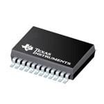
| 封装/外壳 | 24-SOIC(0.295",7.50mm 宽) |
| 封装/箱体 | SOIC-24 Wide |
| 工作温度 | -40°C ~ 85°C |
| 工厂包装数量 | 25 |
| 开关频率 | 450 kHz |
| 拓扑结构 | Full-Bridge, Push-Pull |
| 最大工作温度 | + 85 C |
| 最小工作温度 | - 40 C |
| 标准包装 | 25 |
| 电压-电源 | 9.5 V ~ 20 V |
| 类型 | Current Mode PWM Controllers |
| 系列 | UC2827-1 |
| 输出数 | 3 |
| 输出电流 | 250 mA, 200 mA |
| 输出端数量 | 3 Output |
| 降压 | 无 |
| 隔离式 | 无 |
| 频率-最大值 | 500kHz |


- 商务部:美国ITC正式对集成电路等产品启动337调查
- 曝三星4nm工艺存在良率问题 高通将骁龙8 Gen1或转产台积电
- 太阳诱电将投资9.5亿元在常州建新厂生产MLCC 预计2023年完工
- 英特尔发布欧洲新工厂建设计划 深化IDM 2.0 战略
- 台积电先进制程称霸业界 有大客户加持明年业绩稳了
- 达到5530亿美元!SIA预计今年全球半导体销售额将创下新高
- 英特尔拟将自动驾驶子公司Mobileye上市 估值或超500亿美元
- 三星加码芯片和SET,合并消费电子和移动部门,撤换高东真等 CEO
- 三星电子宣布重大人事变动 还合并消费电子和移动部门
- 海关总署:前11个月进口集成电路产品价值2.52万亿元 增长14.8%


PDF Datasheet 数据手册内容提取
UC2827-1, UC2827-2 UC3827-1, UC3827-2 www.ti.com SLUS365D–APRIL1999–REVISEDAPRIL2011 BUCK CURRENT/VOLTAGE FED PUSH-PULL PWM CONTROLLERS CheckforSamples:UC2827-1,UC2827-2,UC3827-1,UC3827-2 FEATURES 1 DESCRIPTION • IdealforMultipleOutputand/orHigh VoltageOutputVoltageConverters The UC3827 family of controller devices provides an integrated control solution for cascaded buck and • Upto500kHzOperation push-pull converters. These converters are known as • HighVoltage,HighCurrentFloating current fed or voltage fed push-pull converters and DriverforBuckConverterStage are ideally suited for multiple output and/or high • UC3827-1CurrentFedControllerhas voltage output applications. In both current fed and voltage fed modes, the push-pull switches are driven Push-PullDriverswithOverlapping at 50% nominal duty cycles and at one half the ConductionPeriods switching frequency of the buck stage. In the current • UC3827-2VoltageFedControllerhas fed mode, the two switches are driven with a Push-PullDriverswithNonoverlapping specified over-lap period to prevent ringing and ConductionPeriods voltage stress on the devices. In the voltage fed • AverageCurrentMode,PeakCurrent mode, the two switches are driven with a specified gap time between the switches to prevent shorting ModeorVoltageModewithInput the transformer across the energy storage capacitor VoltageFeedforwardControlforBuck and to prohibit excessive currents flowing through the PowerStage devices. • WideBandwidth,LowOffset, The converter's output voltage is regulated by pulse DifferentialCurrentSenseAmplifier width modulation of the buck switch. The UC3827 • PreciseShortCircuitCurrentControl contains complete protection and PWM control functions for the buck converter. Easy control of the floating switch is accomplished by the floating drive circuitry. The gate drive waveform is level shifted to supportaninputvoltageupto72V . DC BLOCKDIAGRAM VEAOCEA+ CEAO RAMP 10 12 6 5 Voltage Error Amplifier VEA+ 14 0.7 V PWM Comparator VEA− 16 CAumrprelinfite Errror + CEA− 13 CSAO 7 +3 V RD FDlryivinegr 1 V+ CSA+ 8 ILIM Comparator S Q 2 BUCK CSA− 9 Current Sense 3 SRC SS 4 Amplifier SS OSC INHBT SYNC 19 UV 21 PGND CT 18 OSC Q DELAY RT 17 50M0A kXHz TQ PDursivhe/Prsull REF 15 24 PUSH VCC 23 REF GND 11 UV&LO UVLO DELAY 22 PULL 20 DELAY 1 Pleasebeawarethatanimportantnoticeconcerningavailability,standardwarranty,anduseincriticalapplicationsofTexas Instrumentssemiconductorproductsanddisclaimerstheretoappearsattheendofthisdatasheet. PRODUCTIONDATAinformationiscurrentasofpublicationdate. Copyright©1999–2011,TexasInstrumentsIncorporated Products conform to specifications per the terms of the Texas Instruments standard warranty. Production processing does not necessarilyincludetestingofallparameters.
UC2827-1, UC2827-2 UC3827-1, UC3827-2 SLUS365D–APRIL1999–REVISEDAPRIL2011 www.ti.com DESCRIPTION (CONTINUED) The UC3827 can be set up in traditional voltage mode control using input voltage feedforward technique or in current mode control. Using current mode control prevents potential core saturation of the push-pull transformer due to mismatches in timing and in component tolerances. With average current mode control, precise control of the inductor current feeding the push-pull stage is possible without the noise sensitivity associated with peak current mode control. The UC3827 average current mode loop can also be connected in parallel with the voltage regulationlooptoassistonlyinfaultconditions. Other valuable features of the UC3827 include bidirectional synchronization capability, user programmable overlap time (UC3827-1), user programmable gap time (UC3827-2), a high bandwidth differential current sense amplifier,andsoftstartcircuitry. ORDERINGINFORMATION(1) PACKAGES T =T PUSH-PULLTOPOLOGY A J SOIC-24 PDIP-24 PLCC-28 CurrentFed UC2827DW-1 UC2827N-1 - -40°Cto85°C VoltageFed UC2827DW-2 UC2827N-2 - CurrentFed UC3827DW-1 UC3827N-1 UC3827Q-1 0°Cto70°C VoltageFed UC3827DW-2 UC3827N-2 - (1) TheDWandQpackagesarealsoavailabletapedandreeled.AddaTRsuffixtothedevicetype(i.e.,UC2827DWTR-1). THERMAL INFORMATION UC2827-1, UC2827-1, UC2827-2, UC2827-2, UC3827-1, UC3827-1, THERMALMETRIC UC3827-2 UC3827-2 UNITS N J 24PINS 24PINS θ Junction-to-ambientthermalresistance(1) 60 70to80 JA °C/W θ Junction-to-case(top)thermalresistance(2) 30 28 JCtop (1) Thejunction-to-ambientthermalresistanceundernaturalconvectionisobtainedinasimulationonaJEDEC-standard,high-Kboard,as specifiedinJESD51-7,inanenvironmentdescribedinJESD51-2a. (2) Thejunction-to-case(top)thermalresistanceisobtainedbysimulatingacoldplatetestonthepackagetop.Nospecific JEDEC-standardtestexists,butaclosedescriptioncanbefoundintheANSISEMIstandardG30-88. THERMAL INFORMATION UC2827-1, UC2827-1, UC2827-2, UC2827-2, UC3827-1, UC3827-1, THERMALMETRIC UC3827-2 UC3827-2 UNITS DW (1)QLCC 28PINS 28PINS θ Junction-to-ambientthermalresistance(2) 71to83 40to65 JA °C/W θ Junction-to-case(top)thermalresistance(3) 24 30 JCtop (1) Formoreinformationabouttraditionalandnewthermalmetrics,seetheICPackageThermalMetricsapplicationreport,SPRA953. (2) Thejunction-to-ambientthermalresistanceundernaturalconvectionisobtainedinasimulationonaJEDEC-standard,high-Kboard,as specifiedinJESD51-7,inanenvironmentdescribedinJESD51-2a. (3) Thejunction-to-case(top)thermalresistanceisobtainedbysimulatingacoldplatetestonthepackagetop.Nospecific JEDEC-standardtestexists,butaclosedescriptioncanbefoundintheANSISEMIstandardG30-88. 2 Copyright©1999–2011,TexasInstrumentsIncorporated
UC2827-1, UC2827-2 UC3827-1, UC3827-2 www.ti.com SLUS365D–APRIL1999–REVISEDAPRIL2011 ABSOLUTE MAXIMUM RATINGS(1) UC2827-1 UC2827-2 UNITS UC3827-1 UC3827-2 Supplyvoltage,VCC 20 CEAO,CEA+,CEA-,CSAO,CSA+,CSA-,CT,DELAY,PUSH,PULL, –0.3to5 RAMP,RT,SS,SYNC,VEA+,VEAO, V Inputvoltagerange V+andBUCK 90 SRC 90-VCC I/Ocontinuous ±250 mA BUCKdriver I/Opeak ±1 A I/Ocontinuous ±200 mA PUSH/PULLdriver I/Opeak ±0.8 A Storagetemperature –65to150 Junctiontemperature –55to150 °C Leadtemperature(soldering,10sec) 300 (1) Voltagesarereferencedtoground.Currentsarepositiveinto,negativeoutofthespecifiedterminal.ConsultPackagingsectionof databookforthermallimitationsandconsiderationsofpackages. ELECTRICAL CHARACTERISTICS Unlessotherwisespsecified,V =15V,V =14.3V,C =340pF,R =10kΩ,R =24.3kΩ,V =V =V = VCC V+ CT RT DELAY SRC GND BUCK V =V outputsnoload,T =T PUSH PULL J A PARAMETER TESTCONDITIONS MIN TYP MAX UNIT SUPPLY VCCUVLO,Turn-on 8.3 8.8 9.5 V Hysteresis 0.9 1.2 1.5 V I Supplycurrentstart V =8V 1000 µA VCC VCC I Supplycurrentrun 32 45 mA VCC I buckhigh 0.2 1 2 mA V+ VOLTAGEERRORAMPLIFIER IB 0.5 3 µA VIO 10 mV AVOL 80 95 dB GBW(1) Gainbandwidth 1 4 MHz V Low-leveloutputvoltage I =0µA(Noload) 0.3 0.5 V OL VEAO V High-leveloutputvoltage I =0µA(Noload) 2.85 3 3.20 V OH VEAO CURRENTSENSEAMPLIFIER IB –1 –5 µA VIO 5 mV AVOL 80 110 dB GBW (1) Gainbandwidth 15 29 MHz V Low-leveloutputvoltage I =0µA(Noload) 0.25 0.5 V OL CEAO V High-leveloutputvoltage I =0µA(Noload) 3 3.3 V OH CEAO CMRR Commonmoderange(1) -0.3 2 V (1) Ensuredbydesign.Notproductiontested. Copyright©1999–2011,TexasInstrumentsIncorporated 3
UC2827-1, UC2827-2 UC3827-1, UC3827-2 SLUS365D–APRIL1999–REVISEDAPRIL2011 www.ti.com ELECTRICAL CHARACTERISTICS (continued) Unlessotherwisespsecified,V =15V,V =14.3V,C =340pF,R =10kΩ,R =24.3kΩ,V =V =V = VCC V+ CT RT DELAY SRC GND BUCK V =V outputsnoload,T =T PUSH PULL J A PARAMETER TESTCONDITIONS MIN TYP MAX UNIT CURRENTERRORAMPLIFIER IB –1 –5 µA VIO 10 mV AVOL 80 110 dB GBW(2) Gainbandwidth At100kHz,MeasureGain 2 4.5 MHz V I =0µA(NoLoad) 0.25 0.5 V OL CEAO V I =0µA(NoLoad) 3.3 3.5 V OH CEAO CMRR Commonmoderange(2) -0.3 5 V OSCILLATORSECTION f Frequency 180 220 250 kHz OSC I CTdischargecurrent 3.5VatCTwhenCTremoved 5 mA CT(dsch) PWMCOMPARATOR D Minimumdutycycle 200kHz 0% MAX D Maximumdutycycle 200kHz 85% 91% 95% MAX BUCKOUTPUTSTAGE t Risetime 1nFLoad(3) 40 100 ns RISE t FalltIme 1nF,Load 30 80 ns FALL I =–15mA,V+–BUCK(4) 1.5 2.5 V BUCK V High-leveloutputvoltage OH IBUCK=–150mA,V+–BUCK (4) 2 2.5 V I =15mA(5) 0.2 0.4 V BUCK V Low-leveloutputvoltage OL I K=150mA(5) 0.7 1.2 V BUC PUSH/PULLOUTPUTSTAGES t Risetime 1nFload 50 100 ns RISE t FalltIme 1nFload 35 100 ns FALL Overlaptime UCx827-1 1nFloads(6) 100 250 400 ns Nonoverlappingtime (7) UCx827-2 100 250 500 ns I =–10mA,VCC–PUSH (P8)USH/PULL 2 3 V V High-leveloutputvoltage OH I =–100mA,VCC– PPUUSSHH/P(U8)LL 2.5 3 V I =10mA(8) 0.2 0.8 V PUSH/PULL V Low-leveloutputvoltage OL I =100mA(8) 0.6 1.2 V PUSH/PULL REFERENCE Referencevoltage 4.8 5 5.2 V I Shor-circuitcurrent V =0V –35 –50 –65 mA SC REF Lineregulation 0.5V<V <20V 5 20 mV VCC Loadregulation 0mA<I <10mA 8 20 mV IO SOFTSTART V Low-leveloutputvoltagesaturation V =7V 250 500 mV OL VCC I Soft-startcurrent –5 –12 –25 µA SS (2) Ensuredbydesign.Notproductiontested. (3) MeasuretherisetimefromwhenBUCKcrosses1Vuntilitcrosses9V. (4) ToforceBUCKhigh,forceV =2.5V,V =2.5V,a25-kΩpulldownresistorfromRAMPtoground,andV =0.5V. CSAO CEAO CT (5) ToforceBUCKlow,forceV =2.5V,V =2.5V,a10-kΩpulldownresistorfromRAMPtoground,andV =3.5V. CSAO CEAO CT (6) TheoverlaptimeismeasuredfromthepointatwhichtherisingedgeofPUSH/PULLcrosses5VuntilthefallingedgeofPULL/PUSH crosses5V. (7) Thenon-overlaptimeismeasuredfromthepointatwhichthefallingedgeofPUSH/PULLcrosses5Vuntiltherisingedgeof PULL/PUSHcrosses5V. (8) TotogglePUSHorPULLintoadesiredstate,pulseCTfrom0.5Vto3.5V.PUSHandPULLtoggleontherisingedgeofCT. 4 Copyright©1999–2011,TexasInstrumentsIncorporated
UC2827-1, UC2827-2 UC3827-1, UC3827-2 www.ti.com SLUS365D–APRIL1999–REVISEDAPRIL2011 CONNECTION DIAGRAMS PLCC-28(QPACKAGE) (TOPVIEW) DIL-24(NorJ,DWPACKAGES) Q PACKAGE (TOPVIEW) (TOP VIEW) N, J OR DW PACKAGES (TOP VIEW) CCK SH C LL RU C + U C U SB N V P V P V+ 1 24 PUSH BUCK 2 23 VCC 4 3 2 1 28 27 26 SS 5 25 PGND SRC 3 22 PULL RAMP 6 24 NC SS 4 21 PGND CEAO 7 23 NC RAMP 5 20 DELAY CEAO 6 19 SYNC CSAO 8 22 DELAY CSAO 7 18 CT CSA+ 9 21 SYNC CSA+ 8 17 RT CSA− 10 20 CT CSA− 9 16 VEA− VEAO 11 19 RT VEAO 10 15 REF 12 1314 15 16 17 18 GND 11 14 VEA+ D + − + F C− CEA+ 12 13 CEA− N A A A E NA G E E E R E C C V V NC − No internal connection TerminalFunctions TERMINAL Nor I/O DESCRIPTION NAME Q DW OutputofthebuckPWMcontroller.TheBUCKoutputisafloatingdriver,optimizedforcontrollingthe BUCK 2 3 O gateofanN-channelMOSFET.Thepeaksinkandsourcecurrentsare1A.V undervoltagefaults CC disablesBUCKtoanoffcondition(low). CEA+ 12 13 I Non-invertinginputofthecurrenterroramplifier. CEA- 13 14 I Invertinginputofthecurrenterroramplifier OutputofthecurrenterroramplifierandtheinvertinginputofthePWMcomparatorofthebuck CEAO 6 7 O converter. CSA+ 8 9 I Noninvertinginputofthecurrentsenseamplifier. CSA– 9 10 I Invertinginputofthecurrentsenseamplifier. Outputofthecurrentsenseamplifierandthenoninvertinginputofthecurrentlimitcomparator.When thesignallevelonthispinexceedsthe3Vthresholdofthecurrentlimitcomparator,thebuckgatedrive CSAO 7 8 O pulseisterminated.Thisfeatureisusefultoimplementcycle-by-cyclecurrentlimitingforthebuck converter. ProvidesforthetimingcapacitorwhichisconnectedbetweenCTandGND.Theoscillatorfrequencyis setbyCTandaresistorRT,connectedbetweenpinRTandGND.TheCTdischargecurrentis CT 18 20 I approximately40xthebiascurrentthroughtheresistorconnectedtoRT.Apracticalmaximumvaluefor thedischargecurrentis20mA.Thefrequencyoftheoscillatorisgivenbyequation(1) AresistortoGNDprogramstheoverlaptimeofthePUSHandPULLoutputsoftheUC3827-1andthe DELAY 20 22 I deadtimeofthePUSHandPULLoutputsoftheUC3827-2.Theminimumvalueoftheresistor,R , DELAY is18kΩ.Thedelayoroverlaptimeisgivenbyequation(2) Groundreferenceforallsensitivesetupcomponentsnotrelatedtodrivingtheoutputs.Theyincludeall GND 11 12 - timing,voltagesense,currentsense,andbypasscomponents. GroundconnectionforthePUSHandPULLoutputs.PGNDmustbeconnectedtoGNDatasinglepoint PGND 21 25 - ontheprintedcircuitboard.Thisisimperativetopreventlarge,highfrequencyswitchingcurrents flowingthroughthegroundmetalizationinsidethedevice. GroundreferencedoutputtodriveanN-channelMOSFET.ThePULLandthePUSHoutputsaredriving PULL 22 26 O thetwoswitchesofthepush-pullconverterwithcomplementarysignalsatclosetoa50%dutycycle. AnyundervoltagefaultswilldisablePULLtoanoffcondition(low). f (cid:2) 0.77 (Hz) OSC R (cid:1)C (1) RT CT R t (cid:3) DELAY(cid:1)10(cid:2)9 (s) (2) DELAY 200(cid:1) Copyright©1999–2011,TexasInstrumentsIncorporated 5
UC2827-1, UC2827-2 UC3827-1, UC3827-2 SLUS365D–APRIL1999–REVISEDAPRIL2011 www.ti.com TerminalFunctions(continued) TERMINAL Nor I/O DESCRIPTION NAME Q DW GroundreferencedoutputtodriveanN-channelMOSFET.ThePULLandthePUSHoutputsaredriving PUSH 24 28 O thetwoswitchesofthepush-pullconverterwithcomplementarysignalsatclosetoa50%dutycycle. AnyundervoltagefaultsdisablesPUSHtoanoffcondition(low). TheRAMPvoltage,aftera700mVinternallevelshift,isfedtothenoninvertinginputofthebuckPWM comparator.AresistortoV andacapacitortoGNDprovideaninputvoltagefeedforwardsignalforthe IN buckcontrollerinvoltagemodecontrol.Inpeakcurrentmodecontrol,theRAMPpinreceivesthe RAMP 5 6 I currentsignalofthebuckconverter.Inanaveragecurrentmodesetup,theRAMPpinhasalinearly increasingrampsignal.ThiswaveformmaybegeneratedeitherbyconnectingRAMPdirectlytoCT,or byconnectingbotharesistorfromVCCtoRAMPandacapacitorfromRAMPtoGND. Theoutputofthe+5Vonboardreference.BypassthispinwithacapacitortoGND.Thereferenceisoff REF 15 16 O whenthechipisinundervoltagelockoutmode.o AresistortoGNDprogramsthechargecurrentofthetimingcapacitorconnectedtoCT.Thecharge currentapproximatelyequalsthatshowninequation(3).Thechargecurrentshouldbelessthan500µA RT 17 19 I tokeepCT'sdischargepeakcurrentlessthan20mA,whichisCT'smaximumpracticaldischargevalue. Thedischargetime,whichsetsthemaximumdutycycle,issetinternallyandisinfluencedbythecharge current. Thesourceconnectionforthefloatingbuckswitch.ThevoltageontheSRCpincanexceedVCCbut SRC 3 4 I mustbelowerthan90V–V .Also,duringturn-offtransientsofthebuckswitch,thevoltageatSRC VCC cangoto–2V. 5Soft-startpinrequiresacapacitortoGND.Duringsoft-starttheoutputofthevoltageerroramplifieris SS 4 5 O clampedtothesoft-startcapacitorvoltagewhichisslowlychargedbyaninternalcurrentsource.In UVLO,SSisheldlow. Abidirectionalpinfortheoscillator.,usedtosynchronizeseveralchipstothefastestoscillator.Itsinput synchronizationthresholdis1.4V.TheSYNCvoltageis3.6Vwhentheoscillatorcapacitor,CT,is SYNC 19 21 I discharged.Otherwiseitis0V.Iftherecommendedsynchronizationcircuitisnotused,a1kΩorlower valueresistorfromSYNCtoGNDmaybeneededtoincreasethefalltimeofthesignalatSYNC. AvoltagesourceconnectedtothispinsuppliesthepowerfortheUC3827.Itisrecommendedtobypass VCC 23 27 I thispintobothGNDandPGNDgroundconnectionswithgoodqualityhighfrequencycapacitors VEA+ 14 15 I Non-invertinginputofthevoltageerroramplifier VEA- 16 18 I Invertinginputofthevoltageerroramplifier VEAO 10 11 O Outputofthevoltageerroramplifier Supplyvoltageforthebuckoutput.ThefloatingdriveroftheUC3827usesthebootstraptechnique whichrequiresareservoircapacitortostoretherequiredenergyfortheontimeofthebuckswitch.A V+ 1 1 I diodemustbeconnectedfromVCCtoV+tochargethereservoircapacitor.Thisdiodemustbeableto withstandV .ThereservoircapacitormustbeconnectedbetweenV+andSRC. IN I (cid:1)2.5V RT R (3) RT 6 Copyright©1999–2011,TexasInstrumentsIncorporated
UC2827-1, UC2827-2 UC3827-1, UC3827-2 www.ti.com SLUS365D–APRIL1999–REVISEDAPRIL2011 APPLICATION INFORMATION VREF OSCILLATOR 2.5 V – RT + VREF 1.4 V RT CT 2.5 V S CT 2.9 V R SYNC 0.5 V 10 k(cid:1) VDG−99086 Figure1. OscillatorBlockWithExternalConnections CIRCUIT BLOCK DESCRIPTION PWMOscillator The oscillator block diagram with external connections is shown in Equation 1. A resistor (R ) connected to pin T RTsetsthelinearchargecurrent: I (cid:1)2.5V RT R RT (1) The timing capacitor (C ) is linearly charged with the charge current forcing the OSC pin to charge to a 3.4 V CT threshold. After exceeding this threshold, the RS flip-flop is set driving CLKSYN high and R low which DEAD discharges C . CT continues to discharge until it reaches a 0.5 V threshold and resets the RS flip-flop which CT repeatsthechargingsequenceasshowninFigure2 As shown in Figure 3, several oscillators are synchronized to the highest free running frequency by connecting 100 pF capacitors in series with each CLKSYN pin and connecting the other side of the capacitors together forming the CLKSYN bus. The CLKSYN bus is then pulled down to ground with a resistance of approximately 10k.ReferringtoFigure1,thesynchronizationthresholdis1.4V.Theoscillatorblanksanysynchronizationpulse that occurs when OSC is below 2.5 V. This allows units, once they discharge below 2.5 V, to continue through the current discharge and subsequent charge cycles whether or not other units on the CLKSYN bus are still synchronizing. This requires the frequency of all free running oscillators to be within 17% of each other to assure synchronization. Copyright©1999–2011,TexasInstrumentsIncorporated 7
UC2827-1, UC2827-2 UC3827-1, UC3827-2 SLUS365D–APRIL1999–REVISEDAPRIL2011 www.ti.com VAO Current Command Charging Discharging 2.9 V OSC 0.5 V THRESHOLD 3.6 V 1.4 V Threshold CLKSYN 8.5 V 0 V OUT VDG−99087 Figure2. OscillatorandPWMOutputWaveform 100 pF SYNC OSC1 100 pF SYNC OSC2 S U B 100 pF N SYNC Y OSC3 S K L C 100 pF SYNC OSC10 10 k(cid:1) VDG−99085 Figure3. OscillatorSynchronizationConnectionDiagram REVISION HISTORY REVISION DATEOFCHANGE DESCRIPTION ImprovedCMRRofCSAfrom(0-2V)to(-0.3-2V) SLUS365A 8/2005 ImprovedCMRRofCEAfrom(0-5V)to(-0.3-5V) SLUS365D 4/2011 UpdatedtheThermalInformationSection 8 Copyright©1999–2011,TexasInstrumentsIncorporated
PACKAGE OPTION ADDENDUM www.ti.com 6-Feb-2020 PACKAGING INFORMATION Orderable Device Status Package Type Package Pins Package Eco Plan Lead/Ball Finish MSL Peak Temp Op Temp (°C) Device Marking Samples (1) Drawing Qty (2) (6) (3) (4/5) UC2827DW-1 ACTIVE SOIC DW 24 25 Green (RoHS NIPDAU Level-3-260C-168 HR -40 to 85 UC2827DW-1 & no Sb/Br) UC2827DW-2 ACTIVE SOIC DW 24 25 Green (RoHS NIPDAU Level-3-260C-168 HR -40 to 85 UC2827DW-2 & no Sb/Br) UC2827DWTR-1 ACTIVE SOIC DW 24 2000 Green (RoHS NIPDAU Level-3-260C-168 HR -40 to 85 UC2827DW-1 & no Sb/Br) UC2827DWTR-1G4 ACTIVE SOIC DW 24 2000 Green (RoHS NIPDAU Level-3-260C-168 HR -40 to 85 UC2827DW-1 & no Sb/Br) UC3827DW-1 ACTIVE SOIC DW 24 25 Green (RoHS NIPDAU Level-3-260C-168 HR 0 to 70 UC3827DW-1 & no Sb/Br) UC3827DW-2 ACTIVE SOIC DW 24 25 Green (RoHS NIPDAU Level-3-260C-168 HR 0 to 70 UC3827DW-2 & no Sb/Br) (1) The marketing status values are defined as follows: ACTIVE: Product device recommended for new designs. LIFEBUY: TI has announced that the device will be discontinued, and a lifetime-buy period is in effect. NRND: Not recommended for new designs. Device is in production to support existing customers, but TI does not recommend using this part in a new design. PREVIEW: Device has been announced but is not in production. Samples may or may not be available. OBSOLETE: TI has discontinued the production of the device. (2) RoHS: TI defines "RoHS" to mean semiconductor products that are compliant with the current EU RoHS requirements for all 10 RoHS substances, including the requirement that RoHS substance do not exceed 0.1% by weight in homogeneous materials. Where designed to be soldered at high temperatures, "RoHS" products are suitable for use in specified lead-free processes. TI may reference these types of products as "Pb-Free". RoHS Exempt: TI defines "RoHS Exempt" to mean products that contain lead but are compliant with EU RoHS pursuant to a specific EU RoHS exemption. Green: TI defines "Green" to mean the content of Chlorine (Cl) and Bromine (Br) based flame retardants meet JS709B low halogen requirements of <=1000ppm threshold. Antimony trioxide based flame retardants must also meet the <=1000ppm threshold requirement. (3) MSL, Peak Temp. - The Moisture Sensitivity Level rating according to the JEDEC industry standard classifications, and peak solder temperature. (4) There may be additional marking, which relates to the logo, the lot trace code information, or the environmental category on the device. (5) Multiple Device Markings will be inside parentheses. Only one Device Marking contained in parentheses and separated by a "~" will appear on a device. If a line is indented then it is a continuation of the previous line and the two combined represent the entire Device Marking for that device. Addendum-Page 1
PACKAGE OPTION ADDENDUM www.ti.com 6-Feb-2020 (6) Lead/Ball Finish - Orderable Devices may have multiple material finish options. Finish options are separated by a vertical ruled line. Lead/Ball Finish values may wrap to two lines if the finish value exceeds the maximum column width. Important Information and Disclaimer:The information provided on this page represents TI's knowledge and belief as of the date that it is provided. TI bases its knowledge and belief on information provided by third parties, and makes no representation or warranty as to the accuracy of such information. Efforts are underway to better integrate information from third parties. TI has taken and continues to take reasonable steps to provide representative and accurate information but may not have conducted destructive testing or chemical analysis on incoming materials and chemicals. TI and TI suppliers consider certain information to be proprietary, and thus CAS numbers and other limited information may not be available for release. In no event shall TI's liability arising out of such information exceed the total purchase price of the TI part(s) at issue in this document sold by TI to Customer on an annual basis. Addendum-Page 2
PACKAGE MATERIALS INFORMATION www.ti.com 15-Jan-2014 TAPE AND REEL INFORMATION *Alldimensionsarenominal Device Package Package Pins SPQ Reel Reel A0 B0 K0 P1 W Pin1 Type Drawing Diameter Width (mm) (mm) (mm) (mm) (mm) Quadrant (mm) W1(mm) UC2827DWTR-1 SOIC DW 24 2000 330.0 24.4 10.75 15.7 2.7 12.0 24.0 Q1 PackMaterials-Page1
PACKAGE MATERIALS INFORMATION www.ti.com 15-Jan-2014 *Alldimensionsarenominal Device PackageType PackageDrawing Pins SPQ Length(mm) Width(mm) Height(mm) UC2827DWTR-1 SOIC DW 24 2000 367.0 367.0 45.0 PackMaterials-Page2
MECHANICAL DATA MPDI008 – OCTOBER 1994 N (R-PDIP-T**) PLASTIC DUAL-IN-LINE PACKAGE 24 PIN SHOWN A 24 13 0.560 (14,22) 0.520 (13,21) 1 12 0.060 (1,52) TYP 0.200 (5,08) MAX 0.610 (15,49) 0.020 (0,51) MIN 0.590 (14,99) Seating Plane 0.100 (2,54) 0.125 (3,18) MIN 0°–15° 0.021 (0,53) 0.010 (0,25) M 0.015 (0,38) 0.010 (0,25) NOM PINS ** 24 28 32 40 48 52 DIM 1.270 1.450 1.650 2.090 2.450 2.650 A MAX (32,26) (36,83) (41,91) (53,09) (62,23) (67,31) 1.230 1.410 1.610 2.040 2.390 2.590 A MIN (31,24) (35,81) (40,89) (51,82) (60,71) (65,79) 4040053/B 04/95 NOTES: A. All linear dimensions are in inches (millimeters). B. This drawing is subject to change without notice. C. Falls within JEDEC MS-011 D. Falls within JEDEC MS-015 (32 pin only) • POST OFFICE BOX 655303 DALLAS, TEXAS 75265
None
None
IMPORTANTNOTICEANDDISCLAIMER TI PROVIDES TECHNICAL AND RELIABILITY DATA (INCLUDING DATASHEETS), DESIGN RESOURCES (INCLUDING REFERENCE DESIGNS), APPLICATION OR OTHER DESIGN ADVICE, WEB TOOLS, SAFETY INFORMATION, AND OTHER RESOURCES “AS IS” AND WITH ALL FAULTS, AND DISCLAIMS ALL WARRANTIES, EXPRESS AND IMPLIED, INCLUDING WITHOUT LIMITATION ANY IMPLIED WARRANTIES OF MERCHANTABILITY, FITNESS FOR A PARTICULAR PURPOSE OR NON-INFRINGEMENT OF THIRD PARTY INTELLECTUAL PROPERTY RIGHTS. These resources are intended for skilled developers designing with TI products. You are solely responsible for (1) selecting the appropriate TI products for your application, (2) designing, validating and testing your application, and (3) ensuring your application meets applicable standards, and any other safety, security, or other requirements. These resources are subject to change without notice. TI grants you permission to use these resources only for development of an application that uses the TI products described in the resource. Other reproduction and display of these resources is prohibited. No license is granted to any other TI intellectual property right or to any third party intellectual property right. TI disclaims responsibility for, and you will fully indemnify TI and its representatives against, any claims, damages, costs, losses, and liabilities arising out of your use of these resources. TI’s products are provided subject to TI’s Terms of Sale (www.ti.com/legal/termsofsale.html) or other applicable terms available either on ti.com or provided in conjunction with such TI products. TI’s provision of these resources does not expand or otherwise alter TI’s applicable warranties or warranty disclaimers for TI products. Mailing Address: Texas Instruments, Post Office Box 655303, Dallas, Texas 75265 Copyright © 2020, Texas Instruments Incorporated