ICGOO在线商城 > 集成电路(IC) > PMIC - 电机驱动器,控制器 > UC2625DW
 Datasheet下载
- 型号: UC2625DW
- 制造商: Texas Instruments
- 库位|库存: xxxx|xxxx
- 要求:
| 数量阶梯 | 香港交货 | 国内含税 |
| +xxxx | $xxxx | ¥xxxx |
查看当月历史价格
查看今年历史价格
UC2625DW产品简介:
ICGOO电子元器件商城为您提供UC2625DW由Texas Instruments设计生产,在icgoo商城现货销售,并且可以通过原厂、代理商等渠道进行代购。 UC2625DW价格参考¥51.16-¥85.72。Texas InstrumentsUC2625DW封装/规格:PMIC - 电机驱动器,控制器, 电机驱动器 功率 MOSFET,功率达林顿管 并联 28-SOIC。您可以下载UC2625DW参考资料、Datasheet数据手册功能说明书,资料中有UC2625DW 详细功能的应用电路图电压和使用方法及教程。
UC2625DW是由Texas Instruments(德州仪器)生产的PMIC(电源管理集成电路),专门用于电机驱动器和控制器。该芯片主要用于直流无刷电机(BLDC)的控制,适用于多种应用场景,尤其是在需要高效、可靠电机控制的系统中。

 应用场景:

1. 家电设备:
   - UC2625DW广泛应用于家用电器如空调、冰箱、洗衣机等。这些设备中的风扇、压缩机和其他电动部件需要精确的电机控制,以实现节能和延长使用寿命。例如,在空调中,它可以用于控制外机风扇和压缩机电机,确保它们在不同工况下平稳运行,同时减少噪音和能耗。

2. 工业自动化:
   - 在工业环境中,UC2625DW可用于驱动各种电机,如伺服电机、步进电机等。它能够提供高精度的速度和位置控制,适用于机器人、传送带、数控机床等设备。通过集成的保护功能(如过流、过温保护),它可以提高系统的可靠性和安全性。

3. 电动工具:
   - 电动工具如电钻、电锯、角磨机等需要高效的电机驱动和控制。UC2625DW可以提供强大的电流驱动能力,并且具备低功耗特性,使得电池供电的电动工具能够在长时间工作时保持高性能和稳定性。

4. 汽车电子:
   - 在汽车领域,UC2625DW可用于电动车窗、座椅调节、雨刷等电机控制。它的高集成度和可靠性使其成为汽车制造商的理想选择,特别是在电动汽车和混合动力汽车中,对电机效率和能效有更高要求的情况下。

5. 消费电子产品:
   - 某些消费电子产品如无人机、智能家居设备等也使用UC2625DW来驱动内部的小型电机。它能够提供紧凑的设计和高效的性能,满足小型化、轻量化的需求。

总之,UC2625DW凭借其高效的电机控制能力和丰富的保护功能,适用于多种需要精确电机控制的应用场景,从家电到工业自动化,再到汽车电子等领域,都能发挥重要作用。
| 参数 | 数值 |
| 产品目录 | 集成电路 (IC)半导体 |
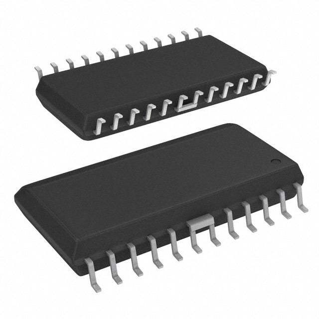
| 描述 | IC MOTOR CONTROLLER PAR 28SOIC马达/运动/点火控制器和驱动器 Brushless DC Motor Controller |
| 产品分类 | PMIC - 电机, 电桥式驱动器集成电路 - IC |
| 品牌 | Texas Instruments |
| 产品手册 | |
| 产品图片 |
|
| rohs | 符合RoHS无铅 / 符合限制有害物质指令(RoHS)规范要求 |
| 产品系列 | 电源管理 IC,马达/运动/点火控制器和驱动器,Texas Instruments UC2625DW- |
| 数据手册 | |
| 产品型号 | UC2625DW |
| 产品 | Brushless DC Motor Controllers |
| 产品目录页面 | |
| 产品种类 | 马达/运动/点火控制器和驱动器 |
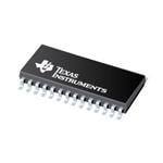
| 供应商器件封装 | 28-SOIC |
| 其它名称 | 296-11162-5 |
| 功能 | 控制器 - 换向,方向管理 |
| 包装 | 管件 |
| 单位重量 | 792 mg |
| 商标 | Texas Instruments |
| 安装类型 | 表面贴装 |
| 安装风格 | SMD/SMT |
| 封装 | Tube |
| 封装/外壳 | 28-SOIC(0.295",7.50mm 宽) |
| 封装/箱体 | SOIC-28 Wide |
| 工作温度 | -40°C ~ 105°C |
| 工作电源电压 | 10 V to 18 V |
| 工厂包装数量 | 20 |
| 应用 | 通用 |
| 接口 | 并联 |
| 标准包装 | 20 |
| 电压-电源 | 10 V ~ 18 V |
| 电压-负载 | - |
| 电机类型-AC,DC | 无刷 DC(BLDC) |
| 电机类型-步进 | - |
| 电流-输出 | - |
| 电源电流 | 14.5 mA |
| 类型 | Brushless DC Motor Controller |
| 系列 | UC2625 |
| 输出配置 | 前级驱动器 |


- 商务部:美国ITC正式对集成电路等产品启动337调查
- 曝三星4nm工艺存在良率问题 高通将骁龙8 Gen1或转产台积电
- 太阳诱电将投资9.5亿元在常州建新厂生产MLCC 预计2023年完工
- 英特尔发布欧洲新工厂建设计划 深化IDM 2.0 战略
- 台积电先进制程称霸业界 有大客户加持明年业绩稳了
- 达到5530亿美元!SIA预计今年全球半导体销售额将创下新高
- 英特尔拟将自动驾驶子公司Mobileye上市 估值或超500亿美元
- 三星加码芯片和SET,合并消费电子和移动部门,撤换高东真等 CEO
- 三星电子宣布重大人事变动 还合并消费电子和移动部门
- 海关总署:前11个月进口集成电路产品价值2.52万亿元 增长14.8%


PDF Datasheet 数据手册内容提取
UC1625 UC2625 UC3625 www.ti.com SLUS353C–NOVEMBER2003–REVISEDJUNE2013 Brushless DC Motor Controller CheckforSamples:UC1625,UC2625,UC3625 FEATURES DESCRIPTION 1 • DrivesPowerMOSFETsorPowerDarlingtons The UC3625 family of motorcontroller devices integrate most of the functions required for high- Directly performance brushless dc-motor control into one • 50-VOpenCollectorHigh-SideDrivers package. When coupled with external power • LatchedSoftStart MOSFETs or Darlingtons, these devices perform • High-SpeedCurrent-SenseAmplifierwithIdeal fixed-frequency PWM motor control in either voltage or current mode while implementing closed-loop Diode speed control and braking with smart noise rejection, • Pulse-by-PulseandAverageCurrentSensing safe direction reversal, and cross–conduction • Over-VoltageandUnder-VoltageProtection protection. • DirectionLatchforSafeDirectionReversal Although specified for operation from power supplies • Tachometer between 10 V and 18 V, the UC1625 controls higher voltage power devices with external level-shifting • TrimmedReferenceSources30mA components. The UC1625 contains fast, high-current • ProgrammableCross-ConductionProtection push-pull drivers for low-side power devices and 50-V • Two-QuadrantandFour-QuadrantOperation open-collector outputs for high-side power devices or level-shiftingcircuitry. The UC1625 is characterized for operation over the military temperature range of –55°C to +125°C, while the UC2625 is characterized from –40°C to +105°C and the UC3625 is characterized from 0°C to +70°C. (Note:ESDProtectionto2kV) TYPICAL APPLICATION +5VTOHALL +15V VMOTOR VREF SENSORS 3kW + 100nF 100nF + 100mF 2N3904 20mF 20mF 10W 10kW QUAD R33OkSWC 3kW 10kW 2 19 11 2N3906 IRF9350 22 3kW DIR 16 6 TO 1k 17 MOTOR 1 TOOTHER CHANNELS 18 28 UC3625 4kW 100nF 27 14 TOOTHER RFOEQRUBIRRAEKDE 13 CHANNELS ANDFAST 2200pF 25 10W IRF532 REVERSE 12 COSC 15 20 BRAKE 21 26 3 24 23 8 9 10 4 5 7 10kW 3nF 68kW 5nF 100nF REQUIRED CT RT 100nF FHRAOLML 240W FAOVERRAGE 2nF SENSORS 5nF 240W 0.W02 CSEUNRSRIENNGT 51kW 2nF RS 0.02 2nF W VREF RD 1 Pleasebeawarethatanimportantnoticeconcerningavailability,standardwarranty,anduseincriticalapplicationsof TexasInstrumentssemiconductorproductsanddisclaimerstheretoappearsattheendofthisdatasheet. PRODUCTIONDATAinformationiscurrentasofpublicationdate. Copyright©2003–2013,TexasInstrumentsIncorporated Products conform to specifications per the terms of the Texas Instruments standard warranty. Production processing does not necessarilyincludetestingofallparameters.
UC1625 UC2625 UC3625 SLUS353C–NOVEMBER2003–REVISEDJUNE2013 www.ti.com ABSOLUTE MAXIMUM RATINGS(1) overoperatingfree-airtemperaturerange(unlessotherwisenoted) VALUE UNIT VCC 20 Pwr Supplyvoltage 20 VCC PWMIN –0.3to+6 E/AIN(+),E/AIN(–) –0.3to+12 V ISENSE1,ISENSE2 –1.3to+6 OV–COAST,DIR,SPEED-IN,SSTART,QUADSEL –0.3to+8 H1,H2,H3 –0.3to+12 PUOutputVoltage –0.3to+50 PU +200continuous PD ±200continuous E/A ±10 I OutputCurrent –10 mA SENSE Tach ±10 Out V –50continuous REF OperatingTemperatureRangeUC1625 –55to+125 T OperatingTemperatureRangeUC2625 –40to+105 °C J OperatingTemperatureRangeUC3625 0to+70 T StorageTemperature –65to+150 °C stg (1) Currentsarepositiveintoandnegativeoutofthespecifiedterminal. 2 SubmitDocumentationFeedback Copyright©2003–2013,TexasInstrumentsIncorporated ProductFolderLinks:UC1625UC2625UC3625
UC1625 UC2625 UC3625 www.ti.com SLUS353C–NOVEMBER2003–REVISEDJUNE2013 Figure1. CONNECTIONDIAGRAM E/AIN(+) 1 28 E/AIN(-) VREF 2 27 E/AOUT ISENSE 3 26 PWMIN ISENSE1 4 25 RC-OSC ISENSE2 5 24 SSTART DIR 6 23 OV-COAST SPEED-IN 7 22 QUADSEL H1 8 21 RC-BRAKE H2 9 20 TACH-OUT H3 10 19 VCC PWRVCC 11 18 PUA PDC 12 17 PUB PDB 13 16 PUC PDA 14 15 GND A. ThispinoutappliestotheSOIC(DW),PLCC(Q),andLCC(L)packages(forexample:pin22hasthesamefunction onallpackages.) Copyright©2003–2013,TexasInstrumentsIncorporated SubmitDocumentationFeedback 3 ProductFolderLinks:UC1625UC2625UC3625
UC1625 UC2625 UC3625 SLUS353C–NOVEMBER2003–REVISEDJUNE2013 www.ti.com ELECTRICAL CHARACTERISTICS Unlessotherwisestated,thesespecificationsapplyfor:T =25°C;PwrV =V =12V;R =20kΩtoV ;C =2nF; A CC CC OSC REF OSC R =33kΩ;C =10nF;andalloutputsunloaded.T =T. TACH TACH A J PARAMETER TESTCONDITIONS MIN TYP MAX UNIT Overall Supplycurrent 14.5 30.0 mA VCCturn-onthreshold Overoperatingrange 8.65 8.95 9.45 V VCCturn-offthreshold 7.75 8.05 8.55 Overvoltage/Coast OV-COASTinhibitthreshold 1.65 1.75 1.85 OV-COASTrestartthreshold 1.55 1.65 1.75 V Overoperatingrange OV-COASThysteresis 0.05 0.10 0.15 OV-COASTinputcurrent -10 -1 0 μA LogicInputs H1,H2,H3lowthreshold 0.8 1.0 1.2 Overoperatingrange V H1,H2,H3highthreshold 1.6 1.9 2.0 H1,H2,H3inputcurrent Overoperatingrange,to0V -400 -250 -120 μA QUADSEL,dirthresholds Overoperatingrange 0.8 1.4 2.0 V QUADSELhysteresis 70 mV DIRhysteresis 0.6 V QUADSELinputcurrent -30 50 150 μA DIRinputcurrent -30 -1 30 PWMAmp/Comparator E/AIN(+),E/AIN(–)inputcurrent To2.5V -5.0 -0.1 5.0 μA PWMINinputcurrent To2.5V 0 3 30 Errorampinputoffset 0V<V <3V -10 10 mV COMMON-MODE Errorampvoltagegain 70 90 dB E/AOUTrange 0.25 3.50 V Pull-upcurrent To0V -16 -10 -5 μA S Dischargecurrent To2.5V 0.1 0.4 3.0 mA START Restartthreshold 0.1 0.2 0.3 V CurrentAmp I =0.3V,I =0.5Vto Gain SENSE1 SENSE2 1.75 1.95 2.15 V/V 0.7V Levelshift I =0.3V,I =0.3V 2.4 2.5 2.65 SENSE1 SENSE2 Peakcurrentthreshold 0.14 0.20 0.26 V I =0V,forceI SENSE1 SENSE2 Overcurrentthreshold 0.26 0.30 0.36 I ,I inputcurrent -850 -320 0 SENSE1 SENSE2 To0V μA I ,I offsetcurrent ±2 ±12 SENSE1 SENSE2 RangeI ,I -1 2 V SENSE1 SENSE2 Tachometer/Brake TACH-OUThighlevel Overoperatingrange,10kΩto2.5 4.7 5 5.3 V TACH-OUTlowlevel V 0.2 Ontime 170 220 280 μs Ontimechangewithtemp Overoperatingrange 0.1% RC-BRAKEinputcurrent To0V -4.0 -1.9 mA Thresholdtobrake,RC-brake Overoperatingrange 0.8 1.0 1.2 V Brakehysteresis,RC-brake 0.09 SPEED-INthreshold Overoperatingrange 220 257 290 mV SPEED-INinputcurrent -30 -5 30 μA 4 SubmitDocumentationFeedback Copyright©2003–2013,TexasInstrumentsIncorporated ProductFolderLinks:UC1625UC2625UC3625
UC1625 UC2625 UC3625 www.ti.com SLUS353C–NOVEMBER2003–REVISEDJUNE2013 ELECTRICAL CHARACTERISTICS (continued) Unlessotherwisestated,thesespecificationsapplyfor:T =25°C;PwrV =V =12V;R =20kΩtoV ;C =2nF; A CC CC OSC REF OSC R =33kΩ;C =10nF;andalloutputsunloaded.T =T. TACH TACH A J PARAMETER TESTCONDITIONS MIN TYP MAX UNIT Low-SideDrivers Voh,–1mA,downfromV 1.60 2.1 CC VVoh,–50mA,downfromV 1.75 2.2 CC Overoperatingrange V Vol,1mA 0.05 0.4 Vol,50mA 0.36 0.8 Rise/falltime 10%to90%slewtime,into1nF 50 ns High-SideDrivers Vol,1mA 0.1 0.4 Overoperatingrange V Vol,50mA 1.0 1.8 Leakagecurrent Outputvoltage=50V 25 μA Falltime 10%to90%slewtime,50mAload 50 ns Oscillator 40 50 60 Frequency kHz Overoperatingrange 35 65 Reference 4.9 5.0 5.1 Outputvoltage V Overoperatingrange 4.7 5.0 5.3 Loadregulation 0mAto–20mAload -40 -5 mV Lineregulation 10Vto18VV -10 -1 10 CC Shortcircuitcurrent Overoperatingrange 50 100 150 mA Miscellaneous Outputturn-ondelay 1 μs Outputturn-offdelay 1 Copyright©2003–2013,TexasInstrumentsIncorporated SubmitDocumentationFeedback 5 ProductFolderLinks:UC1625UC2625UC3625
UC1625 UC2625 UC3625 SLUS353C–NOVEMBER2003–REVISEDJUNE2013 www.ti.com BLOCK DIAGRAM QuadSel 22 5V 2 VREF RC-Osc 25 OSC S Q REFERENCE PWMCLOCK PWMIn 26 R E/AOut 27 E/AIn(+) 1 2.9V E/AIn(–) 28 10mA SSTART 24 ISENSE 3 R Q Q1 ABSVALUE 0.2V 2.5V 250W ISENSE1 4 S 2X ISENSE2 5 3.1V VCC 19 9V PWM OV-Coast 23 CLOCK 18 PUA 1.75V Dir 6 17 PUB DIRECTION Speed-In 7 LATCH 16 PUC 0.25V +5V PWMCLOCK DIR COAST CHOP QUAD 11 PwrVcc H1 8 D Q H1 CROSS 14 PDA CONDUCTION +5V L PROTECTION LATCHES H2 9 D Q H2 DECODER 13 PDB +5V L H3 10 D Q H3 BRAKE L 12 PDC EDGE DETECT 15 GND +5V 2k RC-Brake 21 ONE 20 Tach-Out SHOT 1V 6 SubmitDocumentationFeedback Copyright©2003–2013,TexasInstrumentsIncorporated ProductFolderLinks:UC1625UC2625UC3625
UC1625 UC2625 UC3625 www.ti.com SLUS353C–NOVEMBER2003–REVISEDJUNE2013 DEVICE INFORMATION TerminalFunctions TERMINAL I/O DESCRIPTION NAME NO. ThepositiondecoderlogictranslatestheHallsignalsandtheDIRsignaltothe correctdriversignals(PUsandPDs).Topreventoutputstagedamage,thesignal onDIRisfirstloadedintoadirectionlatch,thenshiftedthroughatwo-bitregister. AslongasSPEED-INislessthan250mV,thedirectionlatchistransparent.When SPEED-INishigherthan250mV,thedirectionlatchinhibitsallchanges indirection.SPEED-INcanbeconnectedtoTACH-OUTthroughafilter,sothatthe directionlatchisonlytransparentwhenthemotorisspinningslowly,andhastoo littlestoredenergytodamagepowerdevices. Additionalcircuitrydetectswhentheinputandoutputofthedirectionlatchare DIR,SPEED-IN 6,7 different,orwhentheinputandoutputoftheshiftregisteraredifferent,andinhibits alloutputdrivesduringthattime.Thiscanbeusedtoallowthemotortocoasttoa safespeedbeforereversing. Theshiftregisterensuresthatdirectioncannotbechangedinstantaneously.The registerisclockedbythePWMoscillator,sothedelaybetweendirectionchanges isalwaysgoingtobebetweenoneandtwooscillatorperiods.At40kHz,this correspondstoadelayofbetween25µsand50µs.Regardlessofoutputstage, 25-µsdeadtimeshouldbeadequatetoensurenooverlapcross-conduction. TogglingDIRcausesanoutputpulseonTACH-OUTregardlessofmotorspeed. E/AIN(+)andE/AIN(–)arenotinternallycommittedtoallowforawidevarietyof uses.TheycanbeconnectedtotheISENSE,toTACH-OUTthroughafilter,toan externalcommandvoltage,toaD/Aconverterforcomputercontrol,ortoanother opampformoreelegantfeedbackloops.Theerroramplifieriscompensatedfor unitygainstability,soE/AOUTcanbetiedtoE/AIN(–)forfeedbackandmajor E/AIN(+),E/AIN(–),E/A 1,28,27, loopcompensation. OUT,PWMIN 26 E/AOUTandPWMIndrivethePWMcomparator.Forvoltage-modePWM systems,PWMIncanbeconnectedtoRC-OSC.ThePWMcomparatorclearsthe PWMlatch,commandingtheoutputstochop. TheerroramplifiercanbebiasedoffbyconnectingE/AIN(–)toahighervoltage than/EAIN(+).Whenbiasedoff,E/AOUTappearstotheapplicationasaresistor toground.E/AOUTcanthenbedrivenbyanexternalamplifier. AllthresholdsandoutputsarereferredtotheGNDpinexceptforthePDandPU GND 15 outputs. Thethreeshaftpositionsensorinputsconsistofhysteresiscomparatorswithinput pull-upresistors.LogicthresholdsmeetTTLspecificationsandcanbedrivenby5- VCMOS,12-VCMOS,NMOS,oropen-collectors. Connecttheseinputstomotorshaftpositionsensorsthatarepositioned120 electricaldegreesapart.Ifnoisysignalsareexpected,zenerclampandfilterthese H1,H2,H3 8,9,10 inputswith6-VzenersandanRCfilter.Suggestedfilteringcomponentsare1kΩ and2nF.Edgeskewinthefilterisnotaproblem,becausesensorsnormally generatemodifiedgraycodewithonlyoneoutputchangingatatime,butriseand falltimesmustbeshorterthan20µsforcorrecttachometeroperation.Motorswith 60electricaldegreepositionsensorcodingcanbeusedifoneortwoofthe positionsensorsignalsisinverted. Thecurrentsenseamplifierhasafixedgainofapproximatelytwo.Italsohasa built-inlevelshiftofapproximately2.5V.ThesignalappearingonISENSEis: I =2.5V+(2×ABS(I -I )) SENSE SENSE1 SENSE2 I andI areinterchangeableandcanbeusedasdifferentialinputs. SENSE1 SENSE2 Thedifferentialsignalappliedcanbeashighas±0.5Vbeforesaturation. IfspikesareexpectedonISENSE1orISENSE2,theyarebestfilteredbya capacitorfromISENSEtoground.Filteringthiswayallowsfastsignalinversionsto becorrectlyprocessedbytheabsolutevaluecircuit.Thepeak-currentcomparator ISENSE1,ISENSE2, 3,4,5 allowsthePWMtoenteracurrent-limitmodewithcurrentinthewindingsnever ISENSE exceedingapproximately0.2V/R .Theovercurrentcomparatorprovidesa SENSE fail-safeshutdownintheunlikelycaseofcurrentexceeding0.3V/R .Then, SENSE softstartiscommanded,andalloutputsareturnedoffuntilthehighcurrent conditionisremoved.ItisoftenessentialtousesomefilterdrivingISENSE1and ISENSE2torejectextremespikesandtocontrolslewrate.Reasonablestarting valuesforfiltercomponentsmightbe250-Ωseriesresistorsanda5-nFcapacitor betweenISENSE1andISENSE2.Inputresistorsshouldbekeptsmalland matchedtomaintaingainaccuracy. Thisinputcanbeusedasanover-voltageshut-downinput,asacoastinput,or OV-COAST 23 both.ThisinputcanbedrivenbyTTL,5-VCMOS,or12-VCMOS. Copyright©2003–2013,TexasInstrumentsIncorporated SubmitDocumentationFeedback 7 ProductFolderLinks:UC1625UC2625UC3625
UC1625 UC2625 UC3625 SLUS353C–NOVEMBER2003–REVISEDJUNE2013 www.ti.com TerminalFunctions(continued) TERMINAL I/O DESCRIPTION NAME NO. TheseoutputscandrivethegatesofN-channelpowerMOSFETsdirectlyorthey candrivethebasesofpowerDarlingtonsifsomeformofcurrentlimitingisused. Theyaremeanttodrivelow-sidepowerdevicesinhigh-currentoutputstages. PDA,PDB,PDC 12,13,14 Currentavailablefromthesepinscanpeakashighas0.5A.Theseoutputsfeature atruetotem-poleoutputstage.Bewareofexceedingdevicepowerdissipation limitswhenusingtheseoutputsforhighcontinuouscurrents.Theseoutputspull hightoturna“low-side”deviceon(activehigh). Theseoutputsareopen-collector,high-voltagedriversthataremeanttodrivehigh- sidepowerdevicesinhigh-currentoutputstages.Theseareactivelowoutputs, meaningthattheseoutputspulllowtocommandahigh-sidedeviceon.These PUA,PUB,PUC 16,17,18 outputscandrivelow-voltagePNPDarlingtonsandP-channelMOSFETsdirectly, andcandriveanyhigh-voltagedeviceusingexternalchargepumptechniques, transformersignalcoupling,cascodelevel-shifttransistors,oropto-isolateddrive (high-speedopto-devicesarerecommended).(Seeapplications). ThissupplypincarriesthecurrentsourcedbythePDoutputs.Whenconnecting PDoutputsdirectlytothebasesofpowerDarlingtons,thePWRVCCpincanbe PWRVCC 11 currentlimitedwitharesistor.Darlingtonoutputscanalsobe"BakerClamped"with diodesfromcollectorsbacktoPWRVCC.(SeeApplications) Thedevicecanchoppowerdevicesineitheroftwomodes,referredtoas“two- quadrant”(QuadSellow)andfourquadrant(QuadSelhigh).Whentwo-quadrant chopping,thepull-downpowerdevicesarechoppedbytheoutputofthePWM latchwhilethepull-updriversremainon.Theloadchopsintoonecommutation diode,andexceptforback-EMF,willexhibitslowdischargecurrentandfaster QUADSEL 22 chargecurrent.Two-quadrantchoppingcanbemoreefficientthanfour-quadrant. Whenfour-quadrantchopping,allpowerdriversarechoppedbythePWMlatch, causingtheloadcurrenttoflowintotwodiodesduringchopping.Thismode exhibitsbettercontrolofloadcurrentwhencurrentislow,andispreferredinservo systemsforequalcontroloveraccelerationanddeceleration.TheQUADSELinput hasnoeffectonoperationduringbraking. EachtimetheTACH-OUTpulses,thecapacitortiedtoRC-BRAKEdischarges fromapproximately3.33Vdownto1.67Vthrougharesistor.Thetachometer pulsewidthisapproximatelyT=0.67R C ,whereR andC arearesistorand T T T T capacitorfromRC-BRAKEtoground.RecommendedvaluesforR are10kΩto T 500kΩ,andrecommendedvaluesforC are1nFto100nF,allowingtimes T between5μsand10ms.Bestaccuracyandstabilityareachievedwithvaluesin thecentersofthoseranges. RC-BRAKEalsohasanotherfunction.IfRC-BRAKEpinispulledbelowthebrake RC-BRAKE 21 threshold,thedeviceentersbrakemode.Thismodeconsistsofturningoffallthree high-sidedevices,enablingallthreelow-sidedevices,anddisablingthe tachometer.Theonlythingsthatinhibitlow-sidedeviceoperationinbrakingare low-supply,exceedingpeakcurrent,OV-COASTcommand,andthePWM comparatorsignal.Thelastofthesemeansthatifcurrentsenseisimplemented suchthatthesignalinthecurrentsenseamplifierisproportionaltobrakingcurrent, thelow-sidedeviceswillbrakethemotorwithcurrentcontrol.(Seeapplications) Simplercurrentsenseconnectionsresultsinuncontrolledbrakingandpotential damagetothepowerdevices. TheUC3625canregulatemotorcurrentusingfixed-frequencypulsewidth modulation(PWM).TheRC-OSCpinsetsoscillatorfrequencybymeansoftiming resistorR fromtheRC-OSCpintoVREFandcapacitorCOSCfromRC-OSC OSC toGnd.Resistors10kΩto100kΩandcapacitors1nFto100nFworksthebest, butfrequencyshouldalwaysbebelow500kHz.Oscillatorfrequencyis approximately: RC-OSC 25 F=2/(R ×C ) OSC OSC Additionalcomponentscanbeaddedtothisdevicetocauseittooperateasa fixedoff-timePWMratherthanafixedfrequencyPWM,usingtheRC-OSCpinto selectthemonostabletimeconstant. ThevoltageontheRC-OSCpinisnormallyarampofabout1.2-Vpeak-to-peak, centeredatapproximately1.6V.Thisrampcanbeusedforvoltage-modePWM control,orcanbeusedforslopecompensationincurrent-modecontrol. 8 SubmitDocumentationFeedback Copyright©2003–2013,TexasInstrumentsIncorporated ProductFolderLinks:UC1625UC2625UC3625
UC1625 UC2625 UC3625 www.ti.com SLUS353C–NOVEMBER2003–REVISEDJUNE2013 TerminalFunctions(continued) TERMINAL I/O DESCRIPTION NAME NO. AnytimethatVCCdropsbelowthresholdorthesensedcurrentexceedstheover- currentthreshold,thesoft-startlatchisset.Whenset,itturnsonatransistorthat pullsdownonSSTART.Normally,acapacitorisconnectedtothispin,andthe transistorwillcompletelydischargethecapacitor.Acomparatorsenseswhenthe NPNtransistorhascompletelydischargedthecapacitor,andallowsthesoft-start latchtoclearwhenthefaultisremoved.Whenthefaultisremoved,thesoft-start capacitorchargesfromtheon-chipcurrentsource. SSTARTclampstheoutputoftheerroramplifier,notallowingtheerroramplifier SSTART 24 outputvoltagetoexceedSSTARTregardlessofinput.TheramponRC-OSCcan beappliedtoPWMInandcomparedtoE/AOUT.WithSSTARTdischargedbelow 0.2Vandtherampminimumbeingapproximately1.0V,thePWMcomparator keepsthePWMlatchclearedandtheoutputsoff.AsSSTARTrises,thePWM comparatorbeginstoduty-cyclemodulatethePWMlatchuntiltheerroramplifier inputsovercometheclamp.Thisprovidesforasafeandorderlymotorstart-up fromanofforfaultcondition.A51-kΩresisterisaddedbetweenVREFand SSTARTtoensureswitching. AnychangeintheH1,H2,orH3inputsloadsdatafromtheseinputsintothe positionsensorlatches.Atthesametimedataisloaded,afixed-width5-Vpulseis triggeredonTACH-OUT.TheaveragevalueofthevoltageonTACH-OUTis directlyproportionaltospeed,sothisoutputcanbeusedasatruetachometerfor speedfeedbackwithanexternalfilteroraveragingcircuitwhichusuallyconsistsof TACH-OUT 20 aresistorandcapacitor. WheneverTACH-OUTishigh,thepositionlatchesareinhibited,suchthatduring thenoisiestpartofthecommutationcycle,additionalcommutationsarenot possible.Althoughthiseffectivelysetsamaximumrotationalspeed,themaximum speedcanbesetabovethehighestexpectedspeed,preventingfalsecommutation andchatter. Thisdeviceoperateswithsuppliesbetween10Vand18V.Under-voltagelockout keepsalloutputsoffbelow7.5V,insuringthattheoutputtransistorsneverturnon VCC 19 untilfulldrivecapabilityisavailable.BypassVCCtogroundwithan0.1-μFceramic capacitor.Usinga10-μFelectrolyticbypasscapacitoraswellcanbebeneficialin applicationswithhighsupplyimpedance. Thispinprovidesregulated5VfordrivingHall-effectdevicesandspeedcontrol circuitry.VREFreaches5VbeforeVCCenables,ensuringthatHall-effectdevices VREF 2 poweredfromVREFbecomesactivebeforetheUC3625drivesanyoutput. AlthoughVREFiscurrentlimited,operationover30mAisnotadvised.Forproper performanceVREFshouldbebypassedwithatleasta0.1-μFcapacitortoground. TYPICAL CHARACTERISTICS OscillatorFrequency TachometeronTime vs vs C andR RTandCT OSC OSC 1MHz 100kHz y c n e u q e r 10kHz F or m at cill s 1kHz O m 100Hz m 0.001 0.01 0.1 m m Figure2. Figure3. Copyright©2003–2013,TexasInstrumentsIncorporated SubmitDocumentationFeedback 9 ProductFolderLinks:UC1625UC2625UC3625
UC1625 UC2625 UC3625 SLUS353C–NOVEMBER2003–REVISEDJUNE2013 www.ti.com TYPICAL CHARACTERISTICS (continued) SupplyCurrent Soft-StartPull-UpCurrent vs vs Temperature Temperature Figure4. Figure5. Soft-StartDischargeCurrent CurrentSenseAmplifierTransferFunction vs vs Temperature I -I SENSE2 SENSE1 Figure6. Figure7. 10 SubmitDocumentationFeedback Copyright©2003–2013,TexasInstrumentsIncorporated ProductFolderLinks:UC1625UC2625UC3625
UC1625 UC2625 UC3625 www.ti.com SLUS353C–NOVEMBER2003–REVISEDJUNE2013 APPLICATION INFORMATION Cross Conduction Prevention TheUC3625insertsdelaystopreventcrossconductionduetooverlappingdrivesignals.However,somethought must always be given to cross conduction in output stage design because no amount of dead time can prevent fastslewingsignalsfromcouplingdrivetoapowerdevicethroughaparasiticcapacitance. TheUC3625containsinputlatchesthatserveasnoiseblankingfilters.Theselatchesremaintransparentthrough any phase of a motor rotation and latch immediately after an input transition is detected. They remain latched for two cycles of the PWM oscillator. At a PWM oscillator speed of 20 kHz, this corresponds to 50 μs to 100 μs of blank time which limits maximum rotational speed to 100 kRPM for a motor with six transitions per rotation or 50 kRPMforamotorwith12transitionsperrotation. This prevents noise generated in the first 50 μs of a transition from propagating to the output transistors and causingcross-conductionorchatter. TheUC3625alsocontainssixflipflopscorrespondingtothesixoutputdrivesignals.Oneoftheseflipflopsisset every time that an output drive signal is turned on, and cleared two PWM oscillator cycles after that drive signal is turned off. The output of each flip flop is used to inhibit drive to the opposing output (Figure 8). In this way, it is impossible to turn on driver PUA and PDA at the same time. It is also impossible for one of these drivers to turn onwithouttheotherdriverhavingbeenoffforatleasttwoPWMoscillatorclocks. EDGE SHIFT S Q FINDER REG PWM R Q PUA CLK PULLUP S Q FROM DECODER R Q PULL PDA DOWN Figure8. CrossConductionPrevention Copyright©2003–2013,TexasInstrumentsIncorporated SubmitDocumentationFeedback 11 ProductFolderLinks:UC1625UC2625UC3625
UC1625 UC2625 UC3625 SLUS353C–NOVEMBER2003–REVISEDJUNE2013 www.ti.com Power Stage Design The UC3625 is useful in a wide variety of applications, including high-power in robotics and machinery. The poweroutputstagesusedinsuchequipmentcantakeanumberofforms,accordingtotheintendedperformance and purpose of the system. Figure 9 show four different power stages with the advantages and disadvantages of each. For high-frequency chopping, fast recovery circulating diodes are essential. Six are required to clamp the windings. These diodes should have a continuous current rating at least equal to the operating motor current, since diode conduction duty-cycle can be high. For low-voltage systems, Schottky diodes are preferred. In higher voltagesystems,diodessuchasMicrosemiUHVPhighvoltageplatinumrectifiersarerecommended. In a pulse-by-pulse current control arrangement, current sensing is done by resistor R , through which the S transistor's currents are passed (Figure A, Figure B, and Figure C of Figure 9). In these cases, R is not needed. D The low-side circulating diodes go to ground and the current sense terminals of the UC3625 (I and I ) SENSE1 SENSE2 areconnectedtoR throughadifferentialRCfilter.Theinputbiascurrentofthecurrentsenseamplifiercausesa S common mode offset voltage to appear at both inputs, so for best accuracy, keep the filter resistors below 2 kΩ andmatched. The current that flows through R is discontinuous because of chopping. It flows during the on time of the power S stage and is zero during the off time. Consequently, the voltage across R consists of a series of pulses, S occurringatthePWMfrequency,withapeakvalueindicativeofthepeakmotorcurrent. To sense average motor current instead of peak current, add another current sense resistor (R in Figure D of D Figure 9) to measure current in the low-side circulating diodes, and operate in four quadrant mode (pin 22 high). The negative voltage across R is corrected by the absolute value current sense amplifier. Within the limitations D imposedbyTable1,thecircuitofFigureBcanalsosenseaveragecurrent. 12 SubmitDocumentationFeedback Copyright©2003–2013,TexasInstrumentsIncorporated ProductFolderLinks:UC1625UC2625UC3625
UC1625 UC2625 UC3625 www.ti.com SLUS353C–NOVEMBER2003–REVISEDJUNE2013 FIGUREA FIGUREB TO TO MOTOR MOTOR R S R S FIGUREC FIGURED TO TO MOTOR MOTOR R R S R D S Figure9. FourPowerStageDesigns Table1.ImposedlimitationsforFigure9 SAFE CURRENTSENSE 2QUADRANT 4QUADRANT POWERREVERSE BRAKING Pulse-by-Pulse Average FigureA Yes No No N0 Yes No FigureB Yes Yes No In4-quadmodeonly Yes Yes FigureC Yes Yes Yes In4-quadmodeonly Yes No FigureD Yes Yes Yes In4-quadmodeonly Yes Yes Copyright©2003–2013,TexasInstrumentsIncorporated SubmitDocumentationFeedback 13 ProductFolderLinks:UC1625UC2625UC3625
UC1625 UC2625 UC3625 SLUS353C–NOVEMBER2003–REVISEDJUNE2013 www.ti.com For drives where speed is critical, P-Channel MOSFETs can be driven by emitter followers as shown in Figure 10. Here, both the level shift NPN and the PNP must withstand high voltages. A zener diode is used to limitgate-sourcevoltageontheMOSFET.Aseriesgateresistorisnotnecessary,butalwaysadvisabletocontrol overshootandringing. High-voltage optocouplers can quickly drive high-voltage MOSFETs if a boost supply of at least 10 V greater than the motor supply is provided (See Figure 11) To protect the MOSFET, the boost supply should not be higherthan18Vabovethemotorsupply. For under 200-V 2-quadrent applications, a power NPN driven by a small P-Channel MOSFET performs well as a high-side driver as in Figure 12. A high voltage small-signal NPN is used as a level shift and a high voltage low-current MOSFET provides drive. Although the NPN will not saturate if used within its limitations, the base- emitterresistorontheNPNisstillthespeedlimitingcomponent. Figure 13 shows a power NPN Darlington drive technique using a clamp to prevent deep saturation. By limiting saturation of the power device, excessive base drive is minimized and turn-off time is kept fairly short. Lack of baseseriesresistancealsoaddstothespeedofthisapproach. Figure10.FastHigh-SideP-ChannelDriver Figure11.OptocoupledN-ChannelHigh-Side Driver 14 SubmitDocumentationFeedback Copyright©2003–2013,TexasInstrumentsIncorporated ProductFolderLinks:UC1625UC2625UC3625
UC1625 UC2625 UC3625 www.ti.com SLUS353C–NOVEMBER2003–REVISEDJUNE2013 Figure12.PowerNPNHigh-SideDriver Figure13.PowerNPNLow-SideDriver Copyright©2003–2013,TexasInstrumentsIncorporated SubmitDocumentationFeedback 15 ProductFolderLinks:UC1625UC2625UC3625
UC1625 UC2625 UC3625 SLUS353C–NOVEMBER2003–REVISEDJUNE2013 www.ti.com Fast High-Side N-Channel Driver with Transformer Isolation A small pulse transformer can provide excellent isolation between the UC3625 and a high-voltage N-Channel MOSFET while also coupling gate drive power. In this circuit (shown in Figure 14), a UC3724 is used as a transformer driver/encoder that duty-cycle modulates the transformer with a 150-kHz pulse train. The UC3725 rectifies this pulse train for gate drive power, demodulates the signal, and drives the gate with over 2-A peak current. +12V VMOTOR 3 33kW 6 7 PUA 2 7 UC3724N UC3725N 4 4 8 1:2 8 1 2 5 1 6 3 5kW 1nF 100nF TOMOTOR Figure14. FastHigh-SideN-ChannelDriverwithTransformerIsolation Both the UC3724 and the UC3725 can operate up to 500 kHz if the pulse transformer is selected appropriately. To raise the operating frequency, either lower the timing resistor of the UC3724 (1 kΩ min), lower the timing capacitoroftheUC3724(500pFmin)orboth. If there is significant capacitance between transformer primary and secondary, together with very high output slew rate, then it may be necessary to add clamp diodes from the transformer primary to 12 V and ground. Generalpurposesmallsignalswitchingdiodessuchas1N4148arenormallyadequate. The UC3725 also has provisions for MOSFET current limiting. Consult the UC3725 data sheet for more informationonimplementingthis. 16 SubmitDocumentationFeedback Copyright©2003–2013,TexasInstrumentsIncorporated ProductFolderLinks:UC1625UC2625UC3625
UC1625 UC2625 UC3625 www.ti.com SLUS353C–NOVEMBER2003–REVISEDJUNE2013 Computational Truth Table Table 2 shows the outputs of the gate drive and open collector outputs for given hall input codes and direction signals.Numbersatthetopofthecolumnsarepinnumbers. These devices operate with position sensor encoding that has either one or two signals high at a time, never all low or all high. This coding is sometimes referred to as 120° Coding because the coding is the same as coding with position sensors spaced 120 magnetic degrees about the rotor. In response to these position sense signals, onlyonelow-sidedriverturnson(gohigh)andonehigh-sidedriverturnson(pulllow)atanytime. Table2.ComputationalTruthTable INPUTS OUTPUTS DIR H1 H2 H3 Low-Side High-Side 6 8 9 10 12 13 14 16 17 18 1 0 0 1 L H L L H H 1 0 1 1 L L H L H H 1 0 1 0 L L H H L H 1 1 1 0 H L L H L H 1 1 0 0 H L L H H L 1 1 0 1 L H L H H L 0 1 0 1 L L H H L H 0 1 0 0 L L H L H H 0 1 1 0 L H L L H H 0 0 1 0 L H L H H L 0 0 1 1 H L L H H L 0 0 0 1 H L L H L H X 1 1 1 L L L H H H X 0 0 0 L L L H H H Copyright©2003–2013,TexasInstrumentsIncorporated SubmitDocumentationFeedback 17 ProductFolderLinks:UC1625UC2625UC3625
UC1625 UC2625 UC3625 SLUS353C–NOVEMBER2003–REVISEDJUNE2013 www.ti.com +5VTOHALL +15V VMOTOR VREF SENSORS 3kW + 100nF 100nF + 100mF 2N3904 20mF 20mF 10W 10kW QUAD R33OkSWC 3kW 10kW 2 19 11 2N3906 IRF9350 22 3kW DIR 16 6 TO 1k 17 MOTOR 1 TOOTHER CHANNELS 18 28 UC3625 4kW 14 REQUIRED 100nF 27 TOOTHER FORBRAKE 13 CHANNELS ANDFAST 2200pF 25 10W IRF532 REVERSE 12 C OSC 15 20 BRAKE 21 26 3 24 23 8 9 10 4 5 7 10kW 3nF 68kW 5nF 100nF REQUIRED CT RT 100nF FHRAOLML 240W FAOVERRAGE 2nF SENSORS 5nF 240W 0.W02 CSEUNRSRIENNGT 51kW 2nF R S 0.02 2nF W R D VREF Figure15. 45-V/8-ABrushlessDCMotorDriveCircuit N-Channel power MOSFETs are used for low-side drivers, while P-Channel power MOSFETs are shown for high-side drivers. Resistors are used to level shift the UC3625 open-collector outputs, driving emitter followers into the MOSFET gate. A 12-V zener clamp insures that the MOSFET gate-source voltage never exceeds 12 V. Series10-Ω gateresistorstamegatereactance,preventingoscillationsandminimizingringing. The oscillator timing capacitor should be placed close to pins 15 and 25, to keep ground current out of the capacitor. Ground current in the timing capacitor causes oscillator distortion and slaving to the commutation signal. The potentiometer connected to pin 1 controls PWM duty cycle directly, implementing a crude form of speed control. This control is often referred to as "voltage mode" because the potentiometer position sets the average motorvoltage.Thiscontrolsspeedbecausesteady-statemotorspeediscloselyrelatedtoappliedvoltage. Pin 20 (Tach-Out) is connected to pin 7 (SPEED IN) through an RC filter, preventing direction reversal while the motor is spinning quickly. In two-quadrant operation, this reversal can cause kinetic energy from the motor to be forcedintothepowerMOSFETs. A diode in series with the low-side MOSFETs facilitates PWM current control during braking by insuring that braking current will not flow backwards through low-side MOSFETs. Dual current-sense resistors give continuous current sense, whether braking or running in four-quadrant operation, an unnecessary luxury for two-quadrant operation. The 68-kΩ and 3-nF tachometer components set maximum commutation time at 140 μs. This permits smooth operationupto35,000RPMforfour-polemotors,yetgives140μsofnoiseblankingaftercommutation. 18 SubmitDocumentationFeedback Copyright©2003–2013,TexasInstrumentsIncorporated ProductFolderLinks:UC1625UC2625UC3625
UC1625 UC2625 UC3625 www.ti.com SLUS353C–NOVEMBER2003–REVISEDJUNE2013 REVISION HISTORY ChangesfromRevisionB(April2007)toRevisionC Page • AddedStorageTemperatureandtemperaturerangetoAbsoluteMaximumRatingsTable ............................................... 2 Copyright©2003–2013,TexasInstrumentsIncorporated SubmitDocumentationFeedback 19 ProductFolderLinks:UC1625UC2625UC3625
PACKAGE OPTION ADDENDUM www.ti.com 6-Feb-2020 PACKAGING INFORMATION Orderable Device Status Package Type Package Pins Package Eco Plan Lead/Ball Finish MSL Peak Temp Op Temp (°C) Device Marking Samples (1) Drawing Qty (2) (6) (3) (4/5) UC2625DW ACTIVE SOIC DW 28 20 Green (RoHS NIPDAU Level-2-260C-1 YEAR -40 to 85 UC2625DW & no Sb/Br) UC2625DWG4 ACTIVE SOIC DW 28 20 Green (RoHS NIPDAU Level-2-260C-1 YEAR -40 to 85 UC2625DW & no Sb/Br) UC2625DWTR ACTIVE SOIC DW 28 1000 Green (RoHS NIPDAU Level-2-260C-1 YEAR -40 to 85 UC2625DW & no Sb/Br) UC3625DW ACTIVE SOIC DW 28 20 Green (RoHS NIPDAU Level-2-260C-1 YEAR 0 to 70 UC3625DW & no Sb/Br) UC3625DWTR ACTIVE SOIC DW 28 1000 Green (RoHS NIPDAU Level-2-260C-1 YEAR 0 to 70 UC3625DW & no Sb/Br) (1) The marketing status values are defined as follows: ACTIVE: Product device recommended for new designs. LIFEBUY: TI has announced that the device will be discontinued, and a lifetime-buy period is in effect. NRND: Not recommended for new designs. Device is in production to support existing customers, but TI does not recommend using this part in a new design. PREVIEW: Device has been announced but is not in production. Samples may or may not be available. OBSOLETE: TI has discontinued the production of the device. (2) RoHS: TI defines "RoHS" to mean semiconductor products that are compliant with the current EU RoHS requirements for all 10 RoHS substances, including the requirement that RoHS substance do not exceed 0.1% by weight in homogeneous materials. Where designed to be soldered at high temperatures, "RoHS" products are suitable for use in specified lead-free processes. TI may reference these types of products as "Pb-Free". RoHS Exempt: TI defines "RoHS Exempt" to mean products that contain lead but are compliant with EU RoHS pursuant to a specific EU RoHS exemption. Green: TI defines "Green" to mean the content of Chlorine (Cl) and Bromine (Br) based flame retardants meet JS709B low halogen requirements of <=1000ppm threshold. Antimony trioxide based flame retardants must also meet the <=1000ppm threshold requirement. (3) MSL, Peak Temp. - The Moisture Sensitivity Level rating according to the JEDEC industry standard classifications, and peak solder temperature. (4) There may be additional marking, which relates to the logo, the lot trace code information, or the environmental category on the device. (5) Multiple Device Markings will be inside parentheses. Only one Device Marking contained in parentheses and separated by a "~" will appear on a device. If a line is indented then it is a continuation of the previous line and the two combined represent the entire Device Marking for that device. (6) Lead/Ball Finish - Orderable Devices may have multiple material finish options. Finish options are separated by a vertical ruled line. Lead/Ball Finish values may wrap to two lines if the finish value exceeds the maximum column width. Addendum-Page 1
PACKAGE OPTION ADDENDUM www.ti.com 6-Feb-2020 Important Information and Disclaimer:The information provided on this page represents TI's knowledge and belief as of the date that it is provided. TI bases its knowledge and belief on information provided by third parties, and makes no representation or warranty as to the accuracy of such information. Efforts are underway to better integrate information from third parties. TI has taken and continues to take reasonable steps to provide representative and accurate information but may not have conducted destructive testing or chemical analysis on incoming materials and chemicals. TI and TI suppliers consider certain information to be proprietary, and thus CAS numbers and other limited information may not be available for release. In no event shall TI's liability arising out of such information exceed the total purchase price of the TI part(s) at issue in this document sold by TI to Customer on an annual basis. OTHER QUALIFIED VERSIONS OF UC2625 : •Enhanced Product: UC2625-EP NOTE: Qualified Version Definitions: •Enhanced Product - Supports Defense, Aerospace and Medical Applications Addendum-Page 2
PACKAGE MATERIALS INFORMATION www.ti.com 29-May-2013 TAPE AND REEL INFORMATION *Alldimensionsarenominal Device Package Package Pins SPQ Reel Reel A0 B0 K0 P1 W Pin1 Type Drawing Diameter Width (mm) (mm) (mm) (mm) (mm) Quadrant (mm) W1(mm) UC2625DWTR SOIC DW 28 1000 330.0 32.4 11.35 18.67 3.1 16.0 32.0 Q1 UC3625DWTR SOIC DW 28 1000 330.0 32.4 11.35 18.67 3.1 16.0 32.0 Q1 PackMaterials-Page1
PACKAGE MATERIALS INFORMATION www.ti.com 29-May-2013 *Alldimensionsarenominal Device PackageType PackageDrawing Pins SPQ Length(mm) Width(mm) Height(mm) UC2625DWTR SOIC DW 28 1000 367.0 367.0 55.0 UC3625DWTR SOIC DW 28 1000 367.0 367.0 55.0 PackMaterials-Page2
IMPORTANTNOTICEANDDISCLAIMER TI PROVIDES TECHNICAL AND RELIABILITY DATA (INCLUDING DATASHEETS), DESIGN RESOURCES (INCLUDING REFERENCE DESIGNS), APPLICATION OR OTHER DESIGN ADVICE, WEB TOOLS, SAFETY INFORMATION, AND OTHER RESOURCES “AS IS” AND WITH ALL FAULTS, AND DISCLAIMS ALL WARRANTIES, EXPRESS AND IMPLIED, INCLUDING WITHOUT LIMITATION ANY IMPLIED WARRANTIES OF MERCHANTABILITY, FITNESS FOR A PARTICULAR PURPOSE OR NON-INFRINGEMENT OF THIRD PARTY INTELLECTUAL PROPERTY RIGHTS. These resources are intended for skilled developers designing with TI products. You are solely responsible for (1) selecting the appropriate TI products for your application, (2) designing, validating and testing your application, and (3) ensuring your application meets applicable standards, and any other safety, security, or other requirements. These resources are subject to change without notice. TI grants you permission to use these resources only for development of an application that uses the TI products described in the resource. Other reproduction and display of these resources is prohibited. No license is granted to any other TI intellectual property right or to any third party intellectual property right. TI disclaims responsibility for, and you will fully indemnify TI and its representatives against, any claims, damages, costs, losses, and liabilities arising out of your use of these resources. TI’s products are provided subject to TI’s Terms of Sale (www.ti.com/legal/termsofsale.html) or other applicable terms available either on ti.com or provided in conjunction with such TI products. TI’s provision of these resources does not expand or otherwise alter TI’s applicable warranties or warranty disclaimers for TI products. Mailing Address: Texas Instruments, Post Office Box 655303, Dallas, Texas 75265 Copyright © 2020, Texas Instruments Incorporated