ICGOO在线商城 > 集成电路(IC) > 接口 - 驱动器,接收器,收发器 > UA9638CP
 Datasheet下载
- 型号: UA9638CP
- 制造商: Texas Instruments
- 库位|库存: xxxx|xxxx
- 要求:
| 数量阶梯 | 香港交货 | 国内含税 |
| +xxxx | $xxxx | ¥xxxx |
查看当月历史价格
查看今年历史价格
UA9638CP产品简介:
ICGOO电子元器件商城为您提供UA9638CP由Texas Instruments设计生产,在icgoo商城现货销售,并且可以通过原厂、代理商等渠道进行代购。 UA9638CP价格参考¥2.21-¥6.36。Texas InstrumentsUA9638CP封装/规格:接口 - 驱动器,接收器,收发器, 驱动器 2/0 RS422,RS485 8-PDIP。您可以下载UA9638CP参考资料、Datasheet数据手册功能说明书,资料中有UA9638CP 详细功能的应用电路图电压和使用方法及教程。
Texas Instruments(德州仪器)的UA9638CP是一款接口驱动器/接收器/收发器芯片,主要应用于高速数据传输和信号调理场景。以下是其典型应用场景:

1. 工业自动化:UA9638CP可用于工业控制系统的通信接口中,例如可编程逻辑控制器(PLC)、分布式控制系统(DCS)以及传感器网络。它支持高可靠性的信号传输,确保在复杂电磁环境下的稳定运行。

2. 通信设备:该芯片适用于各种通信基础设施设备,如路由器、交换机和网关等。它可以实现差分信号的高效驱动与接收,满足长距离或嘈杂环境中的数据通信需求。

3. 汽车电子:在汽车领域,UA9638CP可用于车载网络系统(如CAN总线)以及其他需要高速、低噪声信号传输的应用场合。它的高性能特性有助于提升车辆内部通信的可靠性和速度。

4. 消费类电子产品:某些高端消费级产品(如音频视频设备、智能家居控制器)也可能采用此芯片来优化其接口性能,提供更清晰、更快捷的数据交换能力。

5. 测试测量仪器:在精密测试与测量设备中,UA9638CP能够帮助提高信号完整性和抗干扰能力,从而保证测量结果的准确性。

总之,UA9638CP凭借其优异的电气特性和稳定性,在需要高速、可靠信号传输的各种应用领域中发挥着重要作用。具体选择时还需结合实际电路设计要求及工作条件进行评估。
| 参数 | 数值 |
| 产品目录 | 集成电路 (IC)半导体 |
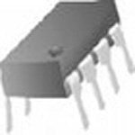
| 描述 | IC DUAL HS DIFF LINE DRVR 8-DIPRS-422接口集成电路 Dual HS Diff |
| 产品分类 | |
| 品牌 | Texas Instruments |
| 产品手册 | |
| 产品图片 |
|
| rohs | 符合RoHS无铅 / 符合限制有害物质指令(RoHS)规范要求 |
| 产品系列 | 接口 IC,RS-422接口集成电路,Texas Instruments UA9638CP- |
| 数据手册 | |
| 产品型号 | UA9638CP |
| 产品目录页面 | |
| 产品种类 | RS-422接口集成电路 |
| 供应商器件封装 | 8-PDIP |
| 其它名称 | 296-15059-5 |
| 功能 | Transmitter |
| 包装 | 管件 |
| 协议 | RS422 |
| 单位重量 | 440.400 mg |
| 双工 | - |
| 商标 | Texas Instruments |
| 安装类型 | 通孔 |
| 安装风格 | Through Hole |
| 封装 | Tube |
| 封装/外壳 | 8-DIP(0.300",7.62mm) |
| 封装/箱体 | PDIP-8 |
| 工作温度 | 0°C ~ 70°C |
| 工作电源电压 | 5.25 V |
| 工厂包装数量 | 50 |
| 接收器滞后 | - |
| 数据速率 | - |
| 最大工作温度 | + 70 C |
| 最小工作温度 | 0 C |
| 标准包装 | 50 |
| 激励器数量 | 1 |
| 电压-电源 | 4.75 V ~ 5.25 V |
| 电源电流 | 65 mA |
| 类型 | 驱动器 |
| 系列 | UA9638 |
| 驱动器/接收器数 | 2/0 |


- 商务部:美国ITC正式对集成电路等产品启动337调查
- 曝三星4nm工艺存在良率问题 高通将骁龙8 Gen1或转产台积电
- 太阳诱电将投资9.5亿元在常州建新厂生产MLCC 预计2023年完工
- 英特尔发布欧洲新工厂建设计划 深化IDM 2.0 战略
- 台积电先进制程称霸业界 有大客户加持明年业绩稳了
- 达到5530亿美元!SIA预计今年全球半导体销售额将创下新高
- 英特尔拟将自动驾驶子公司Mobileye上市 估值或超500亿美元
- 三星加码芯片和SET,合并消费电子和移动部门,撤换高东真等 CEO
- 三星电子宣布重大人事变动 还合并消费电子和移动部门
- 海关总署:前11个月进口集成电路产品价值2.52万亿元 增长14.8%


PDF Datasheet 数据手册内容提取
uA9638C DUAL HIGH-SPEED DIFFERENTIAL LINE DRIVER SLLS112C − OCTOBER 1980 − REVISED APRIL 1994 (cid:2) Meets or Exceeds ANSI Standard D OR P PACKAGE EIA/TIA-422-B (TOP VIEW) (cid:2) Operates From a Single 5-V Power Supply (cid:2) Drives Loads as Low as 50 Ω up V1CAC 12 87 11YZ to 15 Mbps 2A 3 6 2Y (cid:2) TTL- and CMOS-Input Compatibility GND 4 5 2Z (cid:2) Output Short-Circuit Protection (cid:2) Interchangeable With National Semiconductor™ DS9638 description The uA9638C is a dual high-speed differential line driver designed to meet ANSI Standard EIA/TIA-422-B. The inputs are TTL and CMOS compatible and have input clamp diodes. Schottky-diode-clamped transistors are used to minimize propagation delay time. This device operates from a single 5-V power supply and is supplied in an 8-pin package. The uA9638 provides the current needed to drive low-impedance loads at high speeds. Typically used with twisted-pair cabling and differential receiver(s), base-band data transmission can be accomplished up to and exceeding 15 Mbps in properly designed systems. The uA9637A dual line receiver is commonly used as the receiver. For even faster switching speeds in the same pin configuration, see the SN75ALS191. The uA9638C is characterized for operation from 0°C to 70°C. logic symbol† logic diagram 8 8 2 1Y 2 1Y 1A 7 1A 7 1Z 1Z 6 6 3 2Y 3 2Y 2A 5 2A 5 2Z 2Z †This symbol is in accordance with ANSI/IEEE Std 91-1984 and IEC Publication 617-12. Please be aware that an important notice concerning availability, standard warranty, and use in critical applications of TexasInstruments semiconductor products and disclaimers thereto appears at the end of this data sheet. National Semiconductor is a trademark of National Semiconductor Corporation. PRODUCTION DATA information is current as of publication date. Copyright © 1994, Texas Instruments Incorporated Products conform to specifications per the terms of Texas Instruments standard warranty. Production processing does not necessarily include testing of all parameters. POST OFFICE BOX 655303 • DALLAS, TEXAS 75265 1
uA9638C DUAL HIGH-SPEED DIFFERENTIAL LINE DRIVER SLLS112C − OCTOBER 1980 − REVISED APRIL 1994 schematics of inputs and outputs EQUIVALENT OF EACH INPUT TYPICAL OF ALL OUTPUTS VCC VCC 4 kΩ NOM Input 9.6 Ω NOM Output GND absolute maximum ratings over operating free-air temperature range (unless otherwise noted)† Supply voltage range, V (see Note 1) . . . . . . . . . . . . . . . . . . . . . . . . . . . . . . . . . . . . . . . . . . . . . . −0.5 V to 7 V CC Input voltage range, V . . . . . . . . . . . . . . . . . . . . . . . . . . . . . . . . . . . . . . . . . . . . . . . . . . . . . . . . . . . . . . −0.5 V to 7 V I Continuous total power dissipation . . . . . . . . . . . . . . . . . . . . . . . . . . . . . . . . . . . . . See Dissipation Rating Table Operating free-air temperature range, T . . . . . . . . . . . . . . . . . . . . . . . . . . . . . . . . . . . . . . . . . . . . . . . 0°C to 70°C A Storage temperature range, T . . . . . . . . . . . . . . . . . . . . . . . . . . . . . . . . . . . . . . . . . . . . . . . . . . . −65°C to 150°C stg Lead temperature 1,6 mm (1/16 inch) from 10 seconds . . . . . . . . . . . . . . . . . . . . . . . . . . . . . . . . . . . . . . . 260°C †Stresses beyond those listed under “absolute maximum ratings” may cause permanent damage to the device. These are stress ratings only, and functional operation of the device at these or any other conditions beyond those indicated under “recommended operating conditions” is not implied. Exposure to absolute-maximum-rated conditions for extended periods may affect device reliability. NOTE 1: Voltage values except differential output voltages are with respect to network GND. DISSIPATION RATING TABLE PPAACCKKAAGGEE POWTTAAE R== 22R55A°TCCING DDAEEBRROAATTVIIENN GGTA FF =AA 2CC5TT°OOCRR POWTTAAE R== 77R00A°TCCING D 725 mW 5.8 mW/°C 464 mW P 1000 mW 8.0 mW/°C 640 mW recommended operating conditions MIN NOM MAX UNIT Supply voltage, VCC 4.75 5 5.25 V High-level input voltage, VIH 2 V Low-level input voltage, VIL 0.8 V High-level output current, IOH −50 mA Low-level output current, IOL 50 mA Operating free-air temperature, TA 0 70 °C 2 POST OFFICE BOX 655303 • DALLAS, TEXAS 75265
uA9638C DUAL HIGH-SPEED DIFFERENTIAL LINE DRIVER SLLS112C − OCTOBER 1980 − REVISED APRIL 1994 electrical characteristics over operating free-air temperature range (unless otherwise noted) PARAMETER TEST CONDITIONS MIN TYP† MAX UNIT VIK Input clamp voltage VCC = 4.75 V, II = −18 mA −1 −1.2 V VVOH HHiigghh-lleevveell oouuttppuutt vvoollttaaggee VVVCCILCC = == 0 44.8..77 V55 VV,, VVIIHH == 22 VV,, IIOOHH == −−1400 mmAA 2.25 3.5 VV VVOL LLooww-lleevveell oouuttppuutt vvoollttaaggee VVIOCCLCC = == 4 440.. 77m55A VV,, VVIIHH == 22 VV,, VVIILL == 00..88 VV,, 00.55 VV |VOD1| Magnitude of differential output voltage VCC = 5.25 V, IO = 0 2VOD2 V |VOD2| Magnitude of differential output voltage 2 V CChhaannggee iinn mmaaggnniittuuddee ooff ddiiffffeerreennttiiaall ΔΔ||VVOD|| output voltage‡ VVCCCC == 44..7755 VV ttoo 55..2255 VV,, RRLL == 110000 ΩΩ,, ±±00.44 VV VOC Common-mode output voltage§ See Figure 1 3 V CChhaannggee iinn mmaaggnniittuuddee ooff ccoommmmoonn--mmooddee ΔΔ||VVOC|| output voltage‡ ±±00.44 VV VO = 6 V 0.1 100 IIOO OOuuttppuutt ccuurrrreenntt wwiitthh ppoowweerr ooffff VVCCCC = 00 VO = − 0.25 V −0.1 −100 μμAA VO = − 0.25 V to 6 V ±100 II Input current VCC = 5.25 V, VI = 5.5 V 50 μA IIH High-level input current VCC = 5.25 V, VI = 2.7 V 25 μA IIL Low-level input current VCC = 5.25 V, VI = 0.5 V −200 μA IOS Short-circuit output current¶ VCC = 5.25 V, VO = 0 −50 −150 mA ICC Supply current (both drivers) VCC = 5.25 V, No load, All inputs at 0 V 45 65 mA †All typical values are at VCC = 5 V and TA = 25°C. ‡Δ| VOD | and Δ| VOC | are the changes in magnitude of VOD and VOC, respectively, that occur when the input is changed from a high level to a low level or vice versa. §In Standard EIA-422-A, VOC, which is the average of the two output voltages with respect to ground, is called output offset voltage, VOS. ¶Only one output at a time should be shorted, and duration of the short circuit should not exceed one second. switching characteristics, V = 5 V, T = 25°C CC A PARAMETER TEST CONDITIONS MIN TYP MAX UNIT td(OD) Differential output delay time 10 20 ns tt(OD) Differential output transition time CCL = 1155 ppFF, RRL = 110000 ΩΩ, SSeeee FFiigguurree 22 10 20 ns tsk(o) Output skew See Figure 2 1 ns POST OFFICE BOX 655303 • DALLAS, TEXAS 75265 3
uA9638C DUAL HIGH-SPEED DIFFERENTIAL LINE DRIVER SLLS112C − OCTOBER 1980 − REVISED APRIL 1994 PARAMETER MEASUREMENT INFORMATION 50 Ω Input VOD2 50 Ω VOC Figure 1. Differential and Common-Mode Output Voltages 3 V Input 1.5 V 1.5 V 0 V Y Output td(OD) td(OD) Differential 90% 90% CL Output 10% 10% RL = 100 Ω Generator tt(OD) tt(OD) (see Note A) 50 Ω Z Output VOH CL = 15 pF Y Output 50% 50% (see Note B) VOL tsk(o) tsk(o) VOH Z Output 50% 50% VOL TEST CIRCUIT VOLTAGE WAVEFORMS NOTES: A. The input pulse generator has the following characteristics: ZO = 50 Ω, PRR ≤ 500 kHz, tw = 100 ns, tr = ≤ 5 ns. B. CL includes probe and jig capacitance. Figure 2. Test Circuit and Voltage Waveforms 4 POST OFFICE BOX 655303 • DALLAS, TEXAS 75265
PACKAGE OPTION ADDENDUM www.ti.com 6-Feb-2020 PACKAGING INFORMATION Orderable Device Status Package Type Package Pins Package Eco Plan Lead/Ball Finish MSL Peak Temp Op Temp (°C) Device Marking Samples (1) Drawing Qty (2) (6) (3) (4/5) UA9638CD ACTIVE SOIC D 8 75 Green (RoHS NIPDAU Level-2-260C-1 YEAR 0 to 70 9638C & no Sb/Br) UA9638CDE4 ACTIVE SOIC D 8 75 Green (RoHS NIPDAU Level-2-260C-1 YEAR 0 to 70 9638C & no Sb/Br) UA9638CDR ACTIVE SOIC D 8 2500 Green (RoHS NIPDAU Level-2-260C-1 YEAR 0 to 70 9638C & no Sb/Br) UA9638CDRG4 ACTIVE SOIC D 8 2500 Green (RoHS NIPDAU Level-2-260C-1 YEAR 0 to 70 9638C & no Sb/Br) UA9638CP ACTIVE PDIP P 8 50 Green (RoHS NIPDAU N / A for Pkg Type 0 to 70 UA9638CP & no Sb/Br) UA9638CPE4 ACTIVE PDIP P 8 50 Green (RoHS NIPDAU N / A for Pkg Type 0 to 70 UA9638CP & no Sb/Br) (1) The marketing status values are defined as follows: ACTIVE: Product device recommended for new designs. LIFEBUY: TI has announced that the device will be discontinued, and a lifetime-buy period is in effect. NRND: Not recommended for new designs. Device is in production to support existing customers, but TI does not recommend using this part in a new design. PREVIEW: Device has been announced but is not in production. Samples may or may not be available. OBSOLETE: TI has discontinued the production of the device. (2) RoHS: TI defines "RoHS" to mean semiconductor products that are compliant with the current EU RoHS requirements for all 10 RoHS substances, including the requirement that RoHS substance do not exceed 0.1% by weight in homogeneous materials. Where designed to be soldered at high temperatures, "RoHS" products are suitable for use in specified lead-free processes. TI may reference these types of products as "Pb-Free". RoHS Exempt: TI defines "RoHS Exempt" to mean products that contain lead but are compliant with EU RoHS pursuant to a specific EU RoHS exemption. Green: TI defines "Green" to mean the content of Chlorine (Cl) and Bromine (Br) based flame retardants meet JS709B low halogen requirements of <=1000ppm threshold. Antimony trioxide based flame retardants must also meet the <=1000ppm threshold requirement. (3) MSL, Peak Temp. - The Moisture Sensitivity Level rating according to the JEDEC industry standard classifications, and peak solder temperature. (4) There may be additional marking, which relates to the logo, the lot trace code information, or the environmental category on the device. (5) Multiple Device Markings will be inside parentheses. Only one Device Marking contained in parentheses and separated by a "~" will appear on a device. If a line is indented then it is a continuation of the previous line and the two combined represent the entire Device Marking for that device. Addendum-Page 1
PACKAGE OPTION ADDENDUM www.ti.com 6-Feb-2020 (6) Lead/Ball Finish - Orderable Devices may have multiple material finish options. Finish options are separated by a vertical ruled line. Lead/Ball Finish values may wrap to two lines if the finish value exceeds the maximum column width. Important Information and Disclaimer:The information provided on this page represents TI's knowledge and belief as of the date that it is provided. TI bases its knowledge and belief on information provided by third parties, and makes no representation or warranty as to the accuracy of such information. Efforts are underway to better integrate information from third parties. TI has taken and continues to take reasonable steps to provide representative and accurate information but may not have conducted destructive testing or chemical analysis on incoming materials and chemicals. TI and TI suppliers consider certain information to be proprietary, and thus CAS numbers and other limited information may not be available for release. In no event shall TI's liability arising out of such information exceed the total purchase price of the TI part(s) at issue in this document sold by TI to Customer on an annual basis. Addendum-Page 2
PACKAGE MATERIALS INFORMATION www.ti.com 19-Mar-2008 TAPE AND REEL INFORMATION *Alldimensionsarenominal Device Package Package Pins SPQ Reel Reel A0(mm) B0(mm) K0(mm) P1 W Pin1 Type Drawing Diameter Width (mm) (mm) Quadrant (mm) W1(mm) UA9638CDR SOIC D 8 2500 330.0 12.4 6.4 5.2 2.1 8.0 12.0 Q1 PackMaterials-Page1
PACKAGE MATERIALS INFORMATION www.ti.com 19-Mar-2008 *Alldimensionsarenominal Device PackageType PackageDrawing Pins SPQ Length(mm) Width(mm) Height(mm) UA9638CDR SOIC D 8 2500 340.5 338.1 20.6 PackMaterials-Page2
PACKAGE OUTLINE D0008A SOIC - 1.75 mm max height SCALE 2.800 SMALL OUTLINE INTEGRATED CIRCUIT C SEATING PLANE .228-.244 TYP [5.80-6.19] .004 [0.1] C A PIN 1 ID AREA 6X .050 [1.27] 8 1 2X .189-.197 [4.81-5.00] .150 NOTE 3 [3.81] 4X (0 -15 ) 4 5 8X .012-.020 B .150-.157 [0.31-0.51] .069 MAX [3.81-3.98] .010 [0.25] C A B [1.75] NOTE 4 .005-.010 TYP [0.13-0.25] 4X (0 -15 ) SEE DETAIL A .010 [0.25] .004-.010 0 - 8 [0.11-0.25] .016-.050 [0.41-1.27] DETAIL A (.041) TYPICAL [1.04] 4214825/C 02/2019 NOTES: 1. Linear dimensions are in inches [millimeters]. Dimensions in parenthesis are for reference only. Controlling dimensions are in inches. Dimensioning and tolerancing per ASME Y14.5M. 2. This drawing is subject to change without notice. 3. This dimension does not include mold flash, protrusions, or gate burrs. Mold flash, protrusions, or gate burrs shall not exceed .006 [0.15] per side. 4. This dimension does not include interlead flash. 5. Reference JEDEC registration MS-012, variation AA. www.ti.com
EXAMPLE BOARD LAYOUT D0008A SOIC - 1.75 mm max height SMALL OUTLINE INTEGRATED CIRCUIT 8X (.061 ) [1.55] SYMM SEE DETAILS 1 8 8X (.024) [0.6] SYMM (R.002 ) TYP [0.05] 5 4 6X (.050 ) [1.27] (.213) [5.4] LAND PATTERN EXAMPLE EXPOSED METAL SHOWN SCALE:8X SOLDER MASK SOLDER MASK METAL OPENING OPENING METAL UNDER SOLDER MASK EXPOSED METAL EXPOSED METAL .0028 MAX .0028 MIN [0.07] [0.07] ALL AROUND ALL AROUND NON SOLDER MASK SOLDER MASK DEFINED DEFINED SOLDER MASK DETAILS 4214825/C 02/2019 NOTES: (continued) 6. Publication IPC-7351 may have alternate designs. 7. Solder mask tolerances between and around signal pads can vary based on board fabrication site. www.ti.com
EXAMPLE STENCIL DESIGN D0008A SOIC - 1.75 mm max height SMALL OUTLINE INTEGRATED CIRCUIT 8X (.061 ) [1.55] SYMM 1 8 8X (.024) [0.6] SYMM (R.002 ) TYP [0.05] 5 4 6X (.050 ) [1.27] (.213) [5.4] SOLDER PASTE EXAMPLE BASED ON .005 INCH [0.125 MM] THICK STENCIL SCALE:8X 4214825/C 02/2019 NOTES: (continued) 8. Laser cutting apertures with trapezoidal walls and rounded corners may offer better paste release. IPC-7525 may have alternate design recommendations. 9. Board assembly site may have different recommendations for stencil design. www.ti.com
None
IMPORTANTNOTICEANDDISCLAIMER TI PROVIDES TECHNICAL AND RELIABILITY DATA (INCLUDING DATASHEETS), DESIGN RESOURCES (INCLUDING REFERENCE DESIGNS), APPLICATION OR OTHER DESIGN ADVICE, WEB TOOLS, SAFETY INFORMATION, AND OTHER RESOURCES “AS IS” AND WITH ALL FAULTS, AND DISCLAIMS ALL WARRANTIES, EXPRESS AND IMPLIED, INCLUDING WITHOUT LIMITATION ANY IMPLIED WARRANTIES OF MERCHANTABILITY, FITNESS FOR A PARTICULAR PURPOSE OR NON-INFRINGEMENT OF THIRD PARTY INTELLECTUAL PROPERTY RIGHTS. These resources are intended for skilled developers designing with TI products. You are solely responsible for (1) selecting the appropriate TI products for your application, (2) designing, validating and testing your application, and (3) ensuring your application meets applicable standards, and any other safety, security, or other requirements. These resources are subject to change without notice. TI grants you permission to use these resources only for development of an application that uses the TI products described in the resource. Other reproduction and display of these resources is prohibited. No license is granted to any other TI intellectual property right or to any third party intellectual property right. TI disclaims responsibility for, and you will fully indemnify TI and its representatives against, any claims, damages, costs, losses, and liabilities arising out of your use of these resources. TI’s products are provided subject to TI’s Terms of Sale (www.ti.com/legal/termsofsale.html) or other applicable terms available either on ti.com or provided in conjunction with such TI products. TI’s provision of these resources does not expand or otherwise alter TI’s applicable warranties or warranty disclaimers for TI products. Mailing Address: Texas Instruments, Post Office Box 655303, Dallas, Texas 75265 Copyright © 2020, Texas Instruments Incorporated