ICGOO在线商城 > 集成电路(IC) > 接口 - 驱动器,接收器,收发器 > TUSB2551ARGTR
 Datasheet下载
- 型号: TUSB2551ARGTR
- 制造商: Texas Instruments
- 库位|库存: xxxx|xxxx
- 要求:
| 数量阶梯 | 香港交货 | 国内含税 |
| +xxxx | $xxxx | ¥xxxx |
查看当月历史价格
查看今年历史价格
TUSB2551ARGTR产品简介:
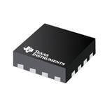
ICGOO电子元器件商城为您提供TUSB2551ARGTR由Texas Instruments设计生产,在icgoo商城现货销售,并且可以通过原厂、代理商等渠道进行代购。 TUSB2551ARGTR价格参考¥4.97-¥11.18。Texas InstrumentsTUSB2551ARGTR封装/规格:接口 - 驱动器,接收器,收发器, 半 收发器 1/3 USB 2.0 16-QFN(3x3)。您可以下载TUSB2551ARGTR参考资料、Datasheet数据手册功能说明书,资料中有TUSB2551ARGTR 详细功能的应用电路图电压和使用方法及教程。
TUSB2551ARGTR 是 Texas Instruments(德州仪器)生产的一款 USB 2.0 高速集线器控制器,属于接口类器件中的驱动器/收发器。该芯片主要用于构建多端口 USB 集线器,支持将一个 USB 接口扩展为多个接口,便于连接多个外设。

其主要应用场景包括:

1. USB 扩展坞与集线器:广泛用于桌面或便携式 USB 集线器设备中,实现对多个 USB 设备的连接和管理;
2. 工业控制设备:在工业自动化系统中作为接口扩展模块,连接多种传感器、执行器或人机界面设备;
3. 嵌入式系统开发板:用于开发板上提供多路 USB 接口,方便调试和外设接入;
4. 消费电子产品:如智能电视、机顶盒等设备中,用于增加 USB 接口数量以连接U盘、鼠标、键盘等外设;
5. 车载电子系统:在车载信息娱乐系统中提供多路 USB 充电和数据传输接口。

该芯片集成度高、功耗低,支持 USB 2.0 高速(480Mbps)通信,具备良好的兼容性和稳定性,适合各类需要 USB 接口扩展的应用场合。
| 参数 | 数值 |
| 产品目录 | 集成电路 (IC)半导体 |
| 描述 | IC TXRX ADVANCED USB 2.0 16QFNUSB 接口集成电路 Advanced Universal Serial Bus Xcvr |
| 产品分类 | |
| 品牌 | Texas Instruments |
| 产品手册 | |
| 产品图片 |
|
| rohs | 符合RoHS无铅 / 符合限制有害物质指令(RoHS)规范要求 |
| 产品系列 | 接口 IC,USB 接口集成电路,Texas Instruments TUSB2551ARGTR- |
| 数据手册 | |
| 产品型号 | TUSB2551ARGTR |
| PCN设计/规格 | |
| 产品目录页面 | |
| 产品种类 | USB 接口集成电路 |
| 供应商器件封装 | 16-QFN(3x3) |
| 其它名称 | 296-24834-1 |
| 包装 | 剪切带 (CT) |
| 协议 | USB 2.0 |
| 单位重量 | 24.100 mg |
| 双工 | 半 |
| 商标 | Texas Instruments |
| 安装类型 | 表面贴装 |
| 安装风格 | SMD/SMT |
| 封装 | Reel |
| 封装/外壳 | 16-VFQFN 裸露焊盘 |
| 封装/箱体 | VQFN-16 |
| 工作温度 | -40°C ~ 85°C |
| 工作电源电压 | 1.65 V to 3.6 V, 3.3 V, 5 V |
| 工作电源电流 | 700 uA, 5 uA |
| 工厂包装数量 | 3000 |
| 接收器滞后 | 200mV |
| 数据速率 | 1.5Mbps |
| 最大工作温度 | + 85 C |
| 最小工作温度 | - 40 C |
| 标准 | USB 2.0 |
| 标准包装 | 1 |
| 电压-电源 | 3.3V,5V |
| 类型 | 收发器 |
| 系列 | TUSB2551A |
| 速度 | High-Speed |
| 驱动器/接收器数 | 1/3 |


.jpg)


- 商务部:美国ITC正式对集成电路等产品启动337调查
- 曝三星4nm工艺存在良率问题 高通将骁龙8 Gen1或转产台积电
- 太阳诱电将投资9.5亿元在常州建新厂生产MLCC 预计2023年完工
- 英特尔发布欧洲新工厂建设计划 深化IDM 2.0 战略
- 台积电先进制程称霸业界 有大客户加持明年业绩稳了
- 达到5530亿美元!SIA预计今年全球半导体销售额将创下新高
- 英特尔拟将自动驾驶子公司Mobileye上市 估值或超500亿美元
- 三星加码芯片和SET,合并消费电子和移动部门,撤换高东真等 CEO
- 三星电子宣布重大人事变动 还合并消费电子和移动部门
- 海关总署:前11个月进口集成电路产品价值2.52万亿元 增长14.8%


PDF Datasheet 数据手册内容提取
TUSB2551A www.ti.com...................................................................................................................................................................................................... SCES790–JUNE2009 ADVANCED UNIVERSAL SERIAL BUS TRANSCEIVER FEATURES 1 • CompliesWithUniversalSerialBus PW PACKAGE SpecificationRev.2.0(USB2.0) (TOPVIEW) • TransmitsandReceivesSerialDataatBoth Full-Speed(12-Mbit/s)andLow-Speed VCC(I/O) 1 14 VCC(5.0) (1.5-Mbit/s)DataRates SPEED 2 13 VPU(3.3) • IntegratedBypassable5-Vto3.3-VVoltage RCV 3 12 Vreg(3.3) VP 4 11 D+ RegulatorforPoweringViaUSBV BUS VM 5 10 D– • Low-PowerOperationisIdealforPortable SOFTCON 6 9 OE Equipment GND 7 8 SUSPEND • MeetstheIEC-61000-4-2ContactDischarge (±9kV)andAir-GapDischarge(±9kV)ESD RGT PACKAGE Ratings (BOTTOMVIEW) • SeparateI/OSupplyWithOperationDownto 1.65V N D O N • Very-LowPowerConsumptiontoMeetUSB TC PE F D S SuspendCurrentRequirements O N U C S G S N • NoPower-SupplySequencingRequirements 5 6 7 8 APPLICATIONS VM 4 9 OE • CellularPhones VP 3 10 D– • PersonalDigitalAssistants(PDAs) GND RCV 2 11 D+ • HandheldComputers (Exposed die pad) SPEED 1 12 Vreg(3.3) 16 15 14 13 C O) 0) 3) N C(I/ C(5. U(3. C C P V V V NC – No internal connection DESCRIPTION/ORDERING INFORMATION The TUSB2551A is a single-chip transceiver that complies with the physical-layer specifications of universal serial bus (USB) 2.0. The device supports both full-speed (12-Mbit/s) and low-speed (1.5-Mbit/s) operation. The TUSB2551A delivers superior edge-rate control, producing crisper eye diagrams, which ease the task of passing USBcompliancetesting. A dual supply-voltage operation allows the TUSB2551A to reference the system interface I/O signals to a supply voltage down to 1.6 V, while independently powered by the USB V . This allows the system interface to CC(5.0) operateatitscorevoltagewithouttheadditionofbufferinglogic,andalsoreducesystemoperatingcurrent. 1 Pleasebeawarethatanimportantnoticeconcerningavailability,standardwarranty,anduseincriticalapplicationsofTexas Instrumentssemiconductorproductsanddisclaimerstheretoappearsattheendofthisdatasheet. UNLESS OTHERWISE NOTED this document contains Copyright©2009,TexasInstrumentsIncorporated PRODUCTION DATA information current as of publication date. Products conform to specifications per the terms of Texas Instruments standard warranty. Production processing does not necessarilyincludetestingofallparameters.
TUSB2551A SCES790–JUNE2009...................................................................................................................................................................................................... www.ti.com ORDERINGINFORMATION(1) T PACKAGE(2) ORDERABLEPARTNUMBER TOP-SIDEMARKING A QFN–RGT Reelof2000 TUSB2551ARGTR ZUH –40°Cto85°C Reelof3000 TUSB2551APWR TSSOP–PW PREVIEW Tubeof90 TUSB2551APW (1) Forthemostcurrentpackageandorderinginformation,seethePackageOptionAddendumattheendofthisdocument,orseetheTI websiteatwww.ti.com. (2) Packagedrawings,thermaldata,andsymbolizationareavailableatwww.ti.com/packaging. BLOCKDIAGRAM To Internal Circuitry LDO V Regulator CC(5.0) V CC(I/O) V reg(3.3) V PU(3.3) SOFTCON D+ SPEED OE D– RCV r o elat Levansl Tr VP VM SUSPEND GND 2 SubmitDocumentationFeedback Copyright©2009,TexasInstrumentsIncorporated ProductFolderLink(s):TUSB2551A
TUSB2551A www.ti.com...................................................................................................................................................................................................... SCES790–JUNE2009 TERMINALFUNCTIONS TERMINAL NO. I/O DESCRIPTION NAME RGT PW Systeminterfacesupplyvoltage.UsedtoprovidereferencesupplyvoltageforsystemI/Ointerface VCC(I/O) 15 1 I signaling. Speed.Edge-ratecontrol:AlogicHIGHoperatesatedgeratesforfull-speedoperation.AlogicLOW SPEED 1 2 I operatesatedgeratesforlow-speedoperation. RCV 2 3 O Receivedata.OutputforUSBdifferentialdata. IfOE=1,VP=Receiveroutput(+) VP 3 4 I/O IfOE=0,VP=Driverinput(+) IfOE=1,VM=Receiveroutput(–) VM 4 5 I/O IfOE=0,VM=Driverinput(–) SOFTCON 5 6 I Softconnect.ControlsstateofVPU(3.3).SeeVPU(3.3)pindescriptionfordetails. GND 6 7 Groundreference SUSPEND 7 8 I Suspend.Activehigh.Turnsoffinternalcircuitstoreducesupplycurrent. NC 8,16 Nointernalconnection Outputenable.Activelow.Enablesthetransceivertotransmitdataontothebus.Wheninactive,the OE 9 9 I transceiverisinthereceivemode. D–,D+ 10,11 10,11 I/O DifferentialdatalinesconformingtotheUSBstandard 3.3-Vreferencesupply.Requiresaminimum0.1-m Fdecouplingcapacitorforstability.A1-m Fcapacitoris Vreg(3.3) 12 12 O recommended. Pullupsupplyvoltage.Usedtoconnect1.5-kΩpullupspeeddetectresistor. VPU(3.3) 13 13 O IfSOFTCON=1,VPU(3.3)ishighimpedance.IfSOFTCON=0,VPU(3.3)=3.3V. VCC(5.0) 14 14 I USBbussupplyvoltage.UsedtopowerUSBtransceiverandinternalcircuitry. FUNCTIONAL DESCRIPTION FUNCTIONSELECTION SUSPEND OE D+,D– RCV VP,VM FUNCTION 0 0 Driving Active Active Normaltransmitmode 0 1 Receiving Active Active Normalreceivemode 1 0 Hi-Z 0 Notactive Lowpowerstate 1 1 Hi-Z 0 Active Receivingduringsuspend(lowpowerstate)(1) (1) Duringsuspend,VPandVMareactivetodetectout-of-bandsignalingconditions. TRUTHTABLEDURINGNORMALMODE OE=0 INPUT OUTPUT RESULT VP VM D+ D– RCV 0 0 0 0 X(1) SE0 0 1 0 1 0 Logic0 1 0 1 0 1 Logic1 1 1 1 1 X(1) Undefined OE=1 INPUT OUTPUT RESULT D+ D– VP VM RCV 0 0 0 0 X(1) SE0 0 1 0 1 0 Logic0 1 0 1 0 1 Logic1 1 1 1 1 X(1) Undefined (1) X=Undefined Copyright©2009,TexasInstrumentsIncorporated SubmitDocumentationFeedback 3 ProductFolderLink(s):TUSB2551A
TUSB2551A SCES790–JUNE2009...................................................................................................................................................................................................... www.ti.com Power-Supply Configurations The TUSB2551A can be used with different power-supply configurations, which can be dynamically changed. An overviewisgiveninTable1. • Normal mode – Both V and V or V and V are connected. For 5-V operation, V is CC(I/O) CC(5.0) CC(5.0) reg(3.3) CC(5.0) connected to a 5-V source (4 V to 5.5 V). The internal voltage regulator then produces 3.3 V for the USB connections. For 3.3-V operation, both V and V are connected to a 3.3-V source (3 V to 3.6 V). CC(5.0) reg(3.3) V is independently connected to a voltage source (1.65 V to 3.6 V), depending on the supply voltage of CC(I/O) theexternalcircuit. • Disable mode – V is not connected; V or V and V are connected. In this mode, the CC(I/O) CC(5.0) CC(5.0) reg(3.3) internalcircuitsoftheTUSB2551Aensurethatthe D+ and D– pins are in 3-state, and the power consumption dropstothelow-power(suspended)statelevel.SomehysteresisisbuiltintothedetectionofV lost. CC(I/O) • Sharing mode – V is connected; V and V are not connected. In this mode, the D+ and D– CC(I/O) CC(5.0) reg(3.3) pins are made 3-state, and the TUSB2551A allows external signals of up to 3.6 V to share the D+ and D– lines. The internal circuits of the TUSB2551A ensure that virtually no current (maximum 10 mA) is drawn via the D+ and D– lines. The power consumption through V drops to the low-power (suspended) state level. CC(I/O) Both the VP and VM pins are driven HIGH to indicate this mode. Pin RCV is made LOW. Some hysteresis is builtintothedetectionofV lost. reg(3.3) Table1.Power-SupplyConfigurationOverview CONFIGURATION VBUS/VTRM VIF Notes MODE Normal Connected Connected Normalsupplyconfigurationandoperation VP/VMareHIGHoutputs,RCVisLOW. Disconnect WithOE=0andSUSPEND=1,datalinesmaybedriven Open Connected (D+/D–sharing) withexternaldevicesupto3.6V. WithD+,D–floating,I drawslessthan1m A. CC(I/O) VP/VMareHIGHoutputs,RCVisLOW. Disconnect Ground Connected WithD+,D–floating,I drawslessthan1m A. CC(I/O)F DisableMode Connected Open LogiccontrolledinputspinsareHi-Z. Prohibited Connected Ground Prohibitedcondition Table2.PinStatesinDisableorSharingMode PINS DISABLE-MODESTATE SHARING-MODESTATE V /V 5-Vinput/3.3-Voutput,3.3-Vinput/3.3-Vinput Notpresent CC(5.0) reg(3.3) V Notpresent 1.65-Vto3.6-Vinput CC(I/O) V Highimpedance(off) Highimpedance(off) PU(3.3) D+,D– Highimpedance Highimpedance VP,VM Invalid(1) H RCV Invalid(1) L Inputs(SPEED,SUSPEND,OE,SOFTCON) Highimpedance Highimpedance (1) HighimpedanceordrivenLOW 4 SubmitDocumentationFeedback Copyright©2009,TexasInstrumentsIncorporated ProductFolderLink(s):TUSB2551A
TUSB2551A www.ti.com...................................................................................................................................................................................................... SCES790–JUNE2009 Power-Supply Input Options TheTUSB2551Ahastwopower-supplyinputoptions. • Internal regulator – V is connected to 4 V to 5.5 V. The internal regulator is used to supply the internal CC(5.0) circuitrywith3.3V(nominal).V becomesa3.3-Voutputreference. reg(3.3) • Regulatorbypass–V andV areconnectedtothesamesupply.Theinternalregulatoris bypassed, CC(5.0) reg(3.3) and the internal circuitry is supplied directly from the V power supply. The voltage range is reg(3.3) 3Vto3.6VtocomplywiththeUSBspecification. Thesupply-voltagerangeforeachinputoptionisspecifiedinTable3. Table3.Power-SupplyInputOptions INPUTOPTION V V V CC(5.0) reg(3.3) CC(I/O) Supplyinputforinternalregulator Voltage-referenceoutput SupplyinputfordigitalI/Opins Internalregualtor (4Vto5.5V) (3.3V,300m A) (1.4Vto3.6V) ConnectedtoV with reg(3.3) Supplyinput SupplyinputfordigitalI/Opins Regulatorbypass maximumvoltagedropof0.3V (3Vto3.6V) (1.4Vto3.6V) (2.7Vto3.6V) Electrostatic Discharge (ESD) PINNAME ESD TYP UNIT IEC61000-4-2,Air-GapDischarge ±9 D+,D–,V IEC61000-4-2,ContactDischarge ±9 kV CC(5.0) Human-BodyModel ±15 Allotherpins Human-BodyModel ±2 kV Copyright©2009,TexasInstrumentsIncorporated SubmitDocumentationFeedback 5 ProductFolderLink(s):TUSB2551A
TUSB2551A SCES790–JUNE2009...................................................................................................................................................................................................... www.ti.com ABSOLUTE MAXIMUM RATINGS(1) overoperatingfree-airtemperaturerange(unlessotherwisenoted) MIN MAX UNIT V Supplyvoltagerange –0.5 6 V CC(5.0) V I/Osupplyvoltagerange –0.5 4.6 V CC(I/O) V Regulatedvoltagerange –0.5 4.6 V reg(3.3) V DCinputvoltagerange –0.5 V +0.5 mA I CC(I/O) I Outputcurrent(D+,D–) ±50 mA O(D+,D-) I Outputcurrent(allothers) ±15 mA O I InputCurrent ±50 mA I T Storagetemperaturerange –65 150 °C stg (1) Stressesbeyondthoselistedunder"absolutemaximumratings"maycausepermanentdamagetothedevice.Thesearestressratings only,andfunctionaloperationofthedeviceattheseoranyotherconditionsbeyondthoseindicatedunder"recommendedoperating conditions"isnotimplied.Exposuretoabsolute-maximum-ratedconditionsforextendedperiodsmayaffectdevicereliability. RECOMMENDED OPERATING CONDITIONS MIN NOM MAX UNIT V Supplyvoltage,internalregulatoroption 5-Voperation 4 5 5.25 V CC(5.0) V Supplyvoltage,regulatorbypassoption 3.3-Voperation 3 3.3 3.6 V reg(3.3) V I/Osupplyvoltage 1.65 3.6 V CC(I/O) V Low-levelinputvoltage(1) V –0.3 0.15V V IL CC(I/O) CC(I/O) V High-levelinputvoltage(1) 0.85V V +0.3 V IH CC(I/O) CC(I/O) D+,D– InputvoltageonanalogI/Opins 0 3.6 V T Junctiontemperature –40 85 °C c (1) Specificationappliestothefollowingpins:SUSPEND,SPEED,RCV,SOFTCON,VP,VM,andOE. 6 SubmitDocumentationFeedback Copyright©2009,TexasInstrumentsIncorporated ProductFolderLink(s):TUSB2551A
TUSB2551A www.ti.com...................................................................................................................................................................................................... SCES790–JUNE2009 DC ELECTRICAL CHARACTERISTICS – SYSTEM AND USB INTERFACE(1) V =3.6V,V =5V(unlessotherwisenoted),T =25°C.Boldindicatesspecificationsovertemperature,–40°Cto CC(I/O) CC(5.0) A 85°C. PARAMETER TESTCONDITIONS MIN TYP MAX UNIT VOH Hvoigltha-gleev(2e)loutput IOH=20m A 0.9VCC(I/O) V VOL Lvoolwta-gleev(e2)loutput IOL=20m A 0.1 V I Inputleakagecurrent(2) –5 1.5 5 m A IL SPEED SUSPEND OE VOLTAGE LOAD 1 0 1 1 5 1 0 0 1 5 0 0 1 1 5 m A V = ICC(I/O) VCC(I/O)supplycurrent 0 0 0 5C.C2(55.0V), 1 5 0 1 0 V = 1 5 CC(I/O) 3.6V f=6MHz, 1 0 0 1 2 mA C =50pF L 0 0 0 f=750kHz, 260 280 m A C =600pF L 1 0 1 800 1100 1 0 0 3000 5000 0 0 1 230 350 m A V = 0 0 0 CC(5.0) 400 700 5.25V, I V supplycurrent CC(5.0) CC(5.0) 0 1 0 V = 130 200 CC(I/O) 3.6V f=6MHz, 1 0 0 6 10 C =50pF L mA f=750kHz, 0 0 0 4..3 5 C =600pF L I V leakagecurrent SOFTCON=1,V =0V –5 5 m A PU(3.3)LEAK PU(3.3) PU(3.3) I V leakagecurrent V =3.6V,V =0V –5 5 m A CC(I/O)LEAK CC(I/O) CC(I/O) CC(5.0) V Pullupoutputvoltage I =200m A,V =4Vto5.25V 3 3.3 3.6 V PU(3.3) reg(3.3) CC(5.0) V switch R PU(3.3) I =10mA,V =4Vto5.25V 10 Ω SW resistance reg(3.3) CC(5.0) ESDProtection IEC-61000-4-2 Air-GapDischarge 10pulses ±9 (D+,D–, kV V only) ContactDischarge 10pulses ±9 CC(5.0) (1) Specificationforpackagedproductonly (2) Specificationappliestothefollowingpins:RCV,VP,VM,OE. Copyright©2009,TexasInstrumentsIncorporated SubmitDocumentationFeedback 7 ProductFolderLink(s):TUSB2551A
TUSB2551A SCES790–JUNE2009...................................................................................................................................................................................................... www.ti.com DC ELECTRICAL CHARACTERISTICS – TRANSCEIVER(1) PARAMETER TESTCONDITIONS MIN TYP MAX UNIT LeakageCurrent I Hi-Zstatedatalineleakage(suspendmode) 0V<V <3.3V,SUSPEND=1 –10 10 m A LO IN InputLevels V Differentialinputsensitivity |(D+)–(D–)| 0.2 V DI V Differentialcommonmoderange IncludesV range 0.8 2.5 V CM DI V Single-endedreceiverthreshold 0.8 2 V SE Receiverhysteresis 200 mV OutputLevels V Staticoutputlow R =1.5kΩto3.6V 0.3 V OL L V Staticoutputhigh R =15kΩtoGND 2.8 3.6 V OH L Capacitance C Transceivercapacitance PintoGND 10 pF IN Z Driveroutputresistance Steady-statedrive 1 6 11 Ω DRV (1) Specificationforpackagedproductonly 8 SubmitDocumentationFeedback Copyright©2009,TexasInstrumentsIncorporated ProductFolderLink(s):TUSB2551A
TUSB2551A www.ti.com...................................................................................................................................................................................................... SCES790–JUNE2009 AC ELECTRICAL CHARACTERISTICS(1) PARAMETER TESTCONDITIONS MIN MAX UNIT DriverCharacteristics(LowSpeed) T Transitionrisetime C =200pF(seeFigure2),C =600pF 75 300 ns R L L T Transitionfalltime C =200pF(seeFigure2),C =600pF 75 300 ns F L L LRFM Rise/falltimematching T ,T 80 125 % R F V Outputsignalcrossovervoltage 1.3 2 V CRS DriverCharacteristics(FullSpeed) T Transitionrisetime C =50pF(seeFigure2) 4 20 ns R L T Transitionfalltime C =50pF(seeFigure2) 4 20 ns F L FRFM Rise/falltimematching TR,TF 90 111.1 % V Outputsignalcrossovervoltage 1.3 2 V CRS TransceiverTiming(FullSpeed) t OEtoreceiver3-statedelay SeeFigure1 15 ns PVZ t Receiver3-statetotransmitdelay SeeFigure1 15 ns PZD t OEtodriver3-statedelay SeeFigure1 15 ns PDZ t Driver3-statetoreceivedelay SeeFigure1 15 ns PZV t PLH V ,V toD+,D–propagationdelay SeeFigure4 17 ns t P M PHL t PLH D+,D–toRCVpropagationdelay SeeFigure3 17 ns t PHL t PLH D+,D–toV ,V propagationdelay SeeFigure3 10 ns t P M PHL (1) Specificationforpackagedproductonly Copyright©2009,TexasInstrumentsIncorporated SubmitDocumentationFeedback 9 ProductFolderLink(s):TUSB2551A
TUSB2551A SCES790–JUNE2009...................................................................................................................................................................................................... www.ti.com TIMINGDIAGRAMS TRANSMIT RECEIVE OE t t PVZ PZV V /V P M t t PZD PDZ D+/D– Figure1.EnableandDisableTimes RISE TIME FALL TIME Differential 90% 90% Data Lines 10% 10% t t R F Figure2.RiseandFallTimes D+ Differential V V CRS Data Lines CRS D– V tPLH tPHL OH V OL V SS Figure3.ReceiverPropagationDelay V OH V OL t t PLH PHL D+ V Differential V CRS Data Lines CRS D– Figure4.DriverPropagationDelay 10 SubmitDocumentationFeedback Copyright©2009,TexasInstrumentsIncorporated ProductFolderLink(s):TUSB2551A
TUSB2551A www.ti.com...................................................................................................................................................................................................... SCES790–JUNE2009 TESTCIRCUITS D.U.T. 25 pF Figure5.LoadforV ,V ,RCV P M VTRM 15k 20 D.U.T. 15k C L Figure6.LoadforD+,D– Copyright©2009,TexasInstrumentsIncorporated SubmitDocumentationFeedback 11 ProductFolderLink(s):TUSB2551A
PACKAGE OPTION ADDENDUM www.ti.com 6-Feb-2020 PACKAGING INFORMATION Orderable Device Status Package Type Package Pins Package Eco Plan Lead/Ball Finish MSL Peak Temp Op Temp (°C) Device Marking Samples (1) Drawing Qty (2) (6) (3) (4/5) TUSB2551ARGTR ACTIVE VQFN RGT 16 3000 Green (RoHS NIPDAU Level-1-260C-UNLIM -40 to 85 ZUH & no Sb/Br) (1) The marketing status values are defined as follows: ACTIVE: Product device recommended for new designs. LIFEBUY: TI has announced that the device will be discontinued, and a lifetime-buy period is in effect. NRND: Not recommended for new designs. Device is in production to support existing customers, but TI does not recommend using this part in a new design. PREVIEW: Device has been announced but is not in production. Samples may or may not be available. OBSOLETE: TI has discontinued the production of the device. (2) RoHS: TI defines "RoHS" to mean semiconductor products that are compliant with the current EU RoHS requirements for all 10 RoHS substances, including the requirement that RoHS substance do not exceed 0.1% by weight in homogeneous materials. Where designed to be soldered at high temperatures, "RoHS" products are suitable for use in specified lead-free processes. TI may reference these types of products as "Pb-Free". RoHS Exempt: TI defines "RoHS Exempt" to mean products that contain lead but are compliant with EU RoHS pursuant to a specific EU RoHS exemption. Green: TI defines "Green" to mean the content of Chlorine (Cl) and Bromine (Br) based flame retardants meet JS709B low halogen requirements of <=1000ppm threshold. Antimony trioxide based flame retardants must also meet the <=1000ppm threshold requirement. (3) MSL, Peak Temp. - The Moisture Sensitivity Level rating according to the JEDEC industry standard classifications, and peak solder temperature. (4) There may be additional marking, which relates to the logo, the lot trace code information, or the environmental category on the device. (5) Multiple Device Markings will be inside parentheses. Only one Device Marking contained in parentheses and separated by a "~" will appear on a device. If a line is indented then it is a continuation of the previous line and the two combined represent the entire Device Marking for that device. (6) Lead/Ball Finish - Orderable Devices may have multiple material finish options. Finish options are separated by a vertical ruled line. Lead/Ball Finish values may wrap to two lines if the finish value exceeds the maximum column width. Important Information and Disclaimer:The information provided on this page represents TI's knowledge and belief as of the date that it is provided. TI bases its knowledge and belief on information provided by third parties, and makes no representation or warranty as to the accuracy of such information. Efforts are underway to better integrate information from third parties. TI has taken and continues to take reasonable steps to provide representative and accurate information but may not have conducted destructive testing or chemical analysis on incoming materials and chemicals. TI and TI suppliers consider certain information to be proprietary, and thus CAS numbers and other limited information may not be available for release. In no event shall TI's liability arising out of such information exceed the total purchase price of the TI part(s) at issue in this document sold by TI to Customer on an annual basis. Addendum-Page 1
PACKAGE MATERIALS INFORMATION www.ti.com 11-Aug-2017 TAPE AND REEL INFORMATION *Alldimensionsarenominal Device Package Package Pins SPQ Reel Reel A0 B0 K0 P1 W Pin1 Type Drawing Diameter Width (mm) (mm) (mm) (mm) (mm) Quadrant (mm) W1(mm) TUSB2551ARGTR VQFN RGT 16 3000 330.0 12.4 3.3 3.3 1.0 8.0 12.0 Q2 PackMaterials-Page1
PACKAGE MATERIALS INFORMATION www.ti.com 11-Aug-2017 *Alldimensionsarenominal Device PackageType PackageDrawing Pins SPQ Length(mm) Width(mm) Height(mm) TUSB2551ARGTR VQFN RGT 16 3000 346.0 346.0 35.0 PackMaterials-Page2
None
PACKAGE OUTLINE RGT0016B VQFN - 1 mm max height SCALE 3.600 PLASTIC QUAD FLATPACK - NO LEAD A 3.1 B 2.9 PIN 1 INDEX AREA 3.1 2.9 1 MAX C SEATING PLANE 0.05 0.08 0.00 1.6 0.05 (0.2) TYP 5 8 EXPOSED THERMAL PAD 12X 0.5 4 9 4X 17 SYMM 1.5 1 12 0.3 16X 0.2 16 13 0.1 C A B PIN 1 ID SYMM (OPTIONAL) 0.05 0.5 16X 0.3 4219033/A 08/2016 NOTES: 1. All linear dimensions are in millimeters. Any dimensions in parenthesis are for reference only. Dimensioning and tolerancing per ASME Y14.5M. 2. This drawing is subject to change without notice. 3. The package thermal pad must be soldered to the printed circuit board for thermal and mechanical performance. www.ti.com
EXAMPLE BOARD LAYOUT RGT0016B VQFN - 1 mm max height PLASTIC QUAD FLATPACK - NO LEAD ( 1.6) SYMM 16 13 16X (0.6) 1 12 16X (0.25) 17 SYMM (2.8) (0.55) TYP 12X (0.5) 9 4 ( 0.2) TYP VIA 5 8 (R0.05) (0.55) TYP ALL PAD CORNERS (2.8) LAND PATTERN EXAMPLE SCALE:20X 0.07 MAX 0.07 MIN ALL AROUND ALL AROUND SOLDER MASK METAL OPENING SOLDER MASK METAL UNDER OPENING SOLDER MASK NON SOLDER MASK SOLDER MASK DEFINED DEFINED (PREFERRED) SOLDER MASK DETAILS 4219033/A 08/2016 NOTES: (continued) 4. This package is designed to be soldered to a thermal pad on the board. For more information, see Texas Instruments literature number SLUA271 (www.ti.com/lit/slua271). 5. Vias are optional depending on application, refer to device data sheet. If any vias are implemented, refer to their locations shown on this view. It is recommended that vias under paste be filled, plugged or tented. www.ti.com
EXAMPLE STENCIL DESIGN RGT0016B VQFN - 1 mm max height PLASTIC QUAD FLATPACK - NO LEAD ( 1.47) 16 13 16X (0.6) 1 12 16X (0.25) 17 SYMM (2.8) 12X (0.5) 9 4 METAL ALL AROUND 5 8 SYMM (R0.05) TYP (2.8) SOLDER PASTE EXAMPLE BASED ON 0.125 mm THICK STENCIL EXPOSED PAD 17: 84% PRINTED SOLDER COVERAGE BY AREA UNDER PACKAGE SCALE:25X 4219033/A 08/2016 NOTES: (continued) 6. Laser cutting apertures with trapezoidal walls and rounded corners may offer better paste release. IPC-7525 may have alternate design recommendations. www.ti.com
IMPORTANTNOTICEANDDISCLAIMER TI PROVIDES TECHNICAL AND RELIABILITY DATA (INCLUDING DATASHEETS), DESIGN RESOURCES (INCLUDING REFERENCE DESIGNS), APPLICATION OR OTHER DESIGN ADVICE, WEB TOOLS, SAFETY INFORMATION, AND OTHER RESOURCES “AS IS” AND WITH ALL FAULTS, AND DISCLAIMS ALL WARRANTIES, EXPRESS AND IMPLIED, INCLUDING WITHOUT LIMITATION ANY IMPLIED WARRANTIES OF MERCHANTABILITY, FITNESS FOR A PARTICULAR PURPOSE OR NON-INFRINGEMENT OF THIRD PARTY INTELLECTUAL PROPERTY RIGHTS. These resources are intended for skilled developers designing with TI products. You are solely responsible for (1) selecting the appropriate TI products for your application, (2) designing, validating and testing your application, and (3) ensuring your application meets applicable standards, and any other safety, security, or other requirements. These resources are subject to change without notice. TI grants you permission to use these resources only for development of an application that uses the TI products described in the resource. Other reproduction and display of these resources is prohibited. No license is granted to any other TI intellectual property right or to any third party intellectual property right. TI disclaims responsibility for, and you will fully indemnify TI and its representatives against, any claims, damages, costs, losses, and liabilities arising out of your use of these resources. TI’s products are provided subject to TI’s Terms of Sale (www.ti.com/legal/termsofsale.html) or other applicable terms available either on ti.com or provided in conjunction with such TI products. TI’s provision of these resources does not expand or otherwise alter TI’s applicable warranties or warranty disclaimers for TI products. Mailing Address: Texas Instruments, Post Office Box 655303, Dallas, Texas 75265 Copyright © 2020, Texas Instruments Incorporated