ICGOO在线商城 > 集成电路(IC) > 线性 - 放大器 - 仪表,运算放大器,缓冲器放大器 > TSZ122IST
 Datasheet下载
- 型号: TSZ122IST
- 制造商: STMicroelectronics
- 库位|库存: xxxx|xxxx
- 要求:
| 数量阶梯 | 香港交货 | 国内含税 |
| +xxxx | $xxxx | ¥xxxx |
查看当月历史价格
查看今年历史价格
TSZ122IST产品简介:
ICGOO电子元器件商城为您提供TSZ122IST由STMicroelectronics设计生产,在icgoo商城现货销售,并且可以通过原厂、代理商等渠道进行代购。 TSZ122IST价格参考。STMicroelectronicsTSZ122IST封装/规格:线性 - 放大器 - 仪表,运算放大器,缓冲器放大器, 零漂移 放大器 2 电路 满摆幅 8-MiniSO。您可以下载TSZ122IST参考资料、Datasheet数据手册功能说明书,资料中有TSZ122IST 详细功能的应用电路图电压和使用方法及教程。
STMicroelectronics的TSZ122IST是一款双路、低噪声、精密运算放大器,属于线性放大器类别,常用于需要高精度信号处理的应用场景。其主要应用场景包括:

1. 传感器信号调理:适用于压力、温度、称重等传感器的微弱信号放大,因其高精度和低噪声特性,可提升测量准确性。

2. 工业自动化与控制系统:用于PLC(可编程逻辑控制器)、工业仪表和过程控制设备中,实现对模拟信号的精确放大与处理。

3. 医疗设备:如心电图仪、血糖仪等便携式或精密医疗检测设备中,用于处理微弱生理信号。

4. 测试与测量仪器:如示波器、万用表、信号发生器等,用于高精度信号放大和处理。

5. 电池供电设备:TSZ122IST具有低功耗特性,适合用于便携式或低功耗系统中,如无线传感器节点、手持式仪器等。

6. 音频与模拟前端电路:在高保真音频设备或模拟信号处理模块中用于前置放大或信号调节。

该器件采用10引脚VSSOP封装,具有宽电源电压范围(2.7V至5.5V)、轨到轨输入输出特性,适合多种应用场景。其高增益带宽积和低失调电压进一步增强了其在精密模拟设计中的适用性。
| 参数 | 数值 |
| -3db带宽 | - |
| 产品目录 | 集成电路 (IC)半导体 |
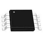
| 描述 | IC OPAMP 5V ZD MICROPWR 8MSOP精密放大器 Very high accuracy 0 drift micropowr 5V |
| 产品分类 | Linear - Amplifiers - Instrumentation, OP Amps, Buffer Amps集成电路 - IC |
| 品牌 | STMicroelectronics |
| 产品手册 | |
| 产品图片 |
|
| rohs | 符合RoHS无铅 / 符合限制有害物质指令(RoHS)规范要求 |
| 产品系列 | 放大器 IC,精密放大器,STMicroelectronics TSZ122IST- |
| mouser_ship_limit | 此产品可能要求许可证才能从美国出口。 |
| 数据手册 | |
| 产品型号 | TSZ122IST |
| 产品种类 | 精密放大器 |
| 供应商器件封装 | 8-MiniSO |
| 共模抑制比—最小值 | 115 dB |
| 其它名称 | 497-14096-6 |
| 包装 | Digi-Reel® |
| 压摆率 | 0.19 V/µs |
| 商标 | STMicroelectronics |
| 增益带宽生成 | 400 kHz |
| 增益带宽积 | 400kHz |
| 安装类型 | 表面贴装 |
| 安装风格 | SMD/SMT |
| 封装 | Reel |
| 封装/外壳 | 8-TSSOP,8-MSOP(0.118",3.00mm 宽) |
| 封装/箱体 | MiniSO-8 |
| 工作温度 | -40°C ~ 125°C |
| 工作电源电压 | 1.8 V to 5.5 V |
| 工厂包装数量 | 4000 |
| 放大器类型 | 通用 |
| 最大工作温度 | + 125 C |
| 最小工作温度 | - 40 C |
| 标准包装 | 1 |
| 特色产品 | http://www.digikey.cn/product-highlights/zh/tsz-ultraprecision-op-amps/52451http://www.digikey.com/product-highlights/cn/zh/stmicroelectronics-high-performance-op-amps/4227 |
| 电压-电源,单/双 (±) | 1.8 V ~ 5.5 V |
| 电压-输入失调 | 1µV |
| 电流-电源 | 31µA |
| 电流-输入偏置 | 70pA |
| 电流-输出/通道 | 18mA |
| 电源电压-最大 | 5.5 V |
| 电源电压-最小 | 1.8 V |
| 电源电流 | 31 uA |
| 电路数 | 2 |
| 系列 | TSZ122 |
| 转换速度 | 0.19 V/us |
| 输入偏压电流—最大 | 300 pA |
| 输入电压范围—最大 | 5.5 V |
| 输入补偿电压 | 1 uV |
| 输出电流 | 18 mA |
| 输出类型 | 满摆幅 |
| 通道数量 | 2 Channel |


- 商务部:美国ITC正式对集成电路等产品启动337调查
- 曝三星4nm工艺存在良率问题 高通将骁龙8 Gen1或转产台积电
- 太阳诱电将投资9.5亿元在常州建新厂生产MLCC 预计2023年完工
- 英特尔发布欧洲新工厂建设计划 深化IDM 2.0 战略
- 台积电先进制程称霸业界 有大客户加持明年业绩稳了
- 达到5530亿美元!SIA预计今年全球半导体销售额将创下新高
- 英特尔拟将自动驾驶子公司Mobileye上市 估值或超500亿美元
- 三星加码芯片和SET,合并消费电子和移动部门,撤换高东真等 CEO
- 三星电子宣布重大人事变动 还合并消费电子和移动部门
- 海关总署:前11个月进口集成电路产品价值2.52万亿元 增长14.8%


PDF Datasheet 数据手册内容提取
TSZ121, TSZ122, TSZ124 Very high accuracy (5 µV) zero drift micropower 5 V operational amplifiers Datasheet - production data Benefits • Higher accuracy without calibration • Accuracy virtually unaffected by temperature change Related products • See TSV711 or TSV731 for continuous-time precision amplifiers Applications • Battery-powered applications • Portable devices • Signal conditioning • Medical instrumentation Description The TSZ12x series of high precision operational amplifiers offer very low input offset voltages with virtually zero drift. Features TSZ121 is the single version, TSZ122 the dual version, and TSZ124 the quad version, with • Very high accuracy and stability: offset pinouts compatible with industry standards. voltage 5 µV max at 25 °C, 8 µV over full temperature range (-40 °C to 125 °C) The TSZ12x series offers rail-to-rail input and • Rail-to-rail input and output output, excellent speed/power consumption ratio, • Low supply voltage: 1.8 - 5.5 V and 400 kHz gain bandwidth product, while • Low power consumption: 40 µA max. at 5 V consuming less than 40 µA at 5 V. The devices • Gain bandwidth product: 400 kHz also feature an ultra-low input bias current. • High tolerance to ESD: 4 kV HBM These features make the TSZ12x family ideal for • Extended temperature range: -40 to 125 °C sensor interfaces, battery-powered applications • Micro-packages: SC70-5, DFN8 2x2, and and portable applications. QFN16 3x3 May 2017 DocID023563 Rev 8 1/35 This is information on a product in full production. www.st.com
Contents TSZ121, TSZ122, TSZ124 Contents 1 Package pin connections ................................................................ 3 2 Absolute maximum ratings and operating conditions ................. 4 3 Electrical characteristics ................................................................ 5 4 Electrical characteristic curves ...................................................... 9 5 Application information ................................................................ 15 5.1 Operation theory ............................................................................. 15 5.1.1 Time domain ..................................................................................... 15 5.1.2 Frequency domain ............................................................................ 16 5.2 Operating voltages .......................................................................... 17 5.3 Input pin voltage ranges .................................................................. 17 5.4 Rail-to-rail input ............................................................................... 17 5.5 Input offset voltage drift over temperature ....................................... 18 5.6 Rail-to-rail output ............................................................................. 18 5.7 Capacitive load ................................................................................ 18 5.8 PCB layout recommendations ......................................................... 19 5.9 Optimized application recommendation .......................................... 19 5.10 EMI rejection ration (EMIRR) .......................................................... 20 5.11 Application examples ...................................................................... 20 5.11.1 Oxygen sensor ................................................................................. 20 5.11.2 Precision instrumentation amplifier .................................................. 21 5.11.3 Low-side current sensing.................................................................. 22 6 Package information ..................................................................... 23 6.1 SC70-5 (or SOT323-5) package information ................................... 24 6.2 SOT23-5 package information ........................................................ 25 6.3 DFN8 2x2 package information ....................................................... 26 6.4 MiniSO8 package information ......................................................... 28 6.5 SO8 package information ................................................................ 29 6.6 QFN16 3x3 package information ..................................................... 30 6.7 TSSOP14 package information ....................................................... 32 7 Ordering information ..................................................................... 33 8 Revision history ............................................................................ 34 2/35 DocID023563 Rev 8
TSZ121, TSZ122, TSZ124 Package pin connections 1 Package pin connections Figure 1: Pin connections for each package (top view) 1. The exposed pads of the DFN8 2x2 and the QFN16 3x3 can be connected to VCC- or left floating. DocID023563 Rev 8 3/35
Absolute maximum ratings and operating TSZ121, TSZ122, TSZ124 conditions 2 Absolute maximum ratings and operating conditions Table 1: Absolute maximum ratings (AMR) Symbol Parameter Value Unit VCC Supply voltage (1) 6 Vid Differential input voltage (2) ±VCC V Vin Input voltage (3) (VCC-) - 0.02. 2to (VCC+) + Iin Input current (4) 10 mA Tstg Storage temperature -65 to 150 °C Tj Maximum junction temperature 150 SC70-5 205 SOT23-5 250 DFN8 2x2 57 Thermal resistance junction to ambient MiniSO8 190 Rthja (5)(6) °C/W SO8 125 QFN16 39 3x3 TSSOP14 100 HBM: human body model (7) 4 kV ESD MM: machine model (8) 300 V CDM: charged device model (9) 1.5 kV Latch-up immunity 200 mA Notes: (1)All voltage values, except the differential voltage are with respect to the network ground terminal. (2)The differential voltage is the non-inverting input terminal with respect to the inverting input terminal. (3)Vcc - Vin must not exceed 6 V, Vin must not exceed 6 V (4)Input current must be limited by a resistor in series with the inputs. (5)Rth are typical values. (6)Short-circuits can cause excessive heating and destructive dissipation. (7)Human body model: 100 pF discharged through a 1.5 kΩ resistor between two pins of the device, done for all couples of pin combinations with other pins floating. (8)Machine model: a 200 pF cap is charged to the specified voltage, then discharged directly between two pins of the device with no external series resistor (internal resistor < 5 Ω), done for all couples of pin combinations with other pins floating. (9)Charged device model: all pins plus package are charged together to the specified voltage and then discharged directly to ground. Table 2: Operating conditions Symbol Parameter Value Unit VCC Supply voltage 1.8 to 5.5 V Vicm Common mode input voltage range (VCC-) - 0.1 to (VCC+) + 0.1 Toper Operating free air temperature range -40 to 125 °C 4/35 DocID023563 Rev 8
TSZ121, TSZ122, TSZ124 Electrical characteristics 3 Electrical characteristics Table 3: Electrical characteristics at VCC+ = 1.8 V with VCC- = 0 V, Vicm = VCC/2, T = 25 ° C, and RL = 10 kΩ connected to VCC/2 (unless otherwise specified) Symbol Parameter Conditions Min. Typ. Max. Unit DC performance T = 25 °C 1 5 Vio Input offset voltage μV -40 °C < T < 125 °C 8 ΔVio/ΔT Input offset voltage drift (1) -40 °C < T < 125 °C 10 30 nV/°C Input bias current T = 25 °C 50 200 (2) Iib (Vout = VCC/2) -40 °C < T < 125 °C 300 (2) pA Input offset current T = 25 °C 100 400 (2) Iio (Vout = VCC/2) -40 °C < T < 125 °C 600 (2) Common mode rejection T = 25 °C 110 122 ratio, 20 log (ΔVicm/ΔVio), CMR Vic = 0 V to VCC, Vout = -40 °C < T < 125 °C 110 VCC/2, RL > 1 MΩ dB Large signal voltage gain, T = 25 °C 118 135 Avd Vout = 0.5 V to (VCC - 0.5 V) -40 °C < T < 125 °C 110 T = 25 °C 30 VOH High-level output voltage -40 °C < T < 125 °C 70 mV T = 25 °C 30 VOL Low-level output voltage -40 °C < T < 125 °C 70 T = 25 °C 7 8 Isink (Vout = VCC) -40 °C < T < 125 °C 6 Iout mA T = 25 °C 5 7 Isource (Vout = 0 V) -40 °C < T < 125 °C 4 Supply current T = 25 °C 28 40 ICC (per amplifier, μA -40 °C < T < 125 °C 40 Vout = VCC/2, RL > 1 MΩ) AC performance GBP Gain bandwidth product 400 kHz Fu Unity gain frequency 300 ɸm Phase margin RL = 10 kΩ, CL = 100 pF 55 Degrees Gm Gain margin 17 dB SR Slew rate (3) 0.17 V/μs ts Setting time To 0.1 %, Vin = 1 Vp-p, RL = 10 50 μs kΩ, CL = 100 pF Equivalent input noise f = 1 kHz 60 en voltage f = 10 kHz 60 nV/√Hz Low-frequency peak-to- ∫en peak input noise Bandwidth, f = 0.1 to 10 Hz 1.1 µVpp Cs Channel separation f = 100 Hz 120 dB DocID023563 Rev 8 5/35
Electrical characteristics TSZ121, TSZ122, TSZ124 Symbol Parameter Conditions Min. Typ. Max. Unit T = 25 °C 50 tinit Initialization time μs -40 °C < T < 125 °C 100 Notes: (1)See Section 5.5: "Input offset voltage drift over temperature". Input offset measurements are performed on x100 gain configuration. The amplifiers and the gain setting resistors are at the same temperature. (2)Guaranteed by design (3)Slew rate value is calculated as the average between positive and negative slew rates. Table 4: Electrical characteristics at VCC+ = 3.3 V with VCC- = 0 V, Vicm = VCC/2, T = 25 ° C, and RL = 10 kΩ connected to VCC/2 (unless otherwise specified) Symbol Parameter Conditions Min. Typ. Max. Unit DC performance T = 25 °C 1 5 Vio Input offset voltage μV -40 °C < T < 125 °C 8 ΔVio/ΔT Input offset voltage drift (1) -40 °C < T < 125 °C 10 30 nV/°C Input bias current T = 25 °C 60 200 (2) Iib (Vout = VCC/2) -40 °C < T < 125 °C 300 (2) pA Input offset current T = 25 °C 120 400 (2) Iio (Vout = VCC/2) -40 °C < T < 125 °C 600 (2) Common mode rejection T = 25 °C 115 128 ratio, 20 log (ΔVicm/ΔVio), CMR Vic = 0 V to VCC, Vout = -40 °C < T < 125 °C 115 VCC/2, RL > 1 MΩ dB Large signal voltage gain, T = 25 °C 118 135 Avd Vout = 0.5 V to (VCC - 0.5 V) -40 °C < T < 125 °C 110 T = 25 °C 30 VOH High-level output voltage -40 °C < T < 125 °C 70 mV T = 25 °C 30 VOL Low-level output voltage -40 °C < T < 125 °C 70 T = 25 °C 15 18 Isink (Vout = VCC) -40 °C < T < 125 °C 12 Iout mA T = 25 °C 14 16 Isource (Vout = 0 V) -40 °C < T < 125 °C 10 Supply current (per T = 25 °C 29 40 ICC amplifier, μA -40 °C < T < 125 °C 40 Vout = VCC/2, RL > 1 MΩ) AC performance GBP Gain bandwidth product 400 kHz Fu Unity gain frequency 300 ɸm Phase margin RL = 10 kΩ, CL = 100 pF 56 Degrees Gm Gain margin 19 dB SR Slew rate (3) 0.19 V/μs 6/35 DocID023563 Rev 8
TSZ121, TSZ122, TSZ124 Electrical characteristics Symbol Parameter Conditions Min. Typ. Max. Unit To 0.1 %, Vin = 1 Vp-p, RL = 10 ts Setting time kΩ, CL = 100 pF 50 μs Equivalent input noise f = 1 kHz 40 en nV/√Hz voltage f = 10 kHz 40 Low-frequency peak-to- ∫en peak input noise Bandwidth, f = 0.1 to 10 Hz 0.8 µVpp Cs Channel separation f = 100 Hz 120 dB T = 25 °C 50 tinit Initialization time μs -40 °C < T < 125 °C 100 Notes: (1)See Section 5.5: "Input offset voltage drift over temperature". Input offset measurements are performed on x100 gain configuration. The amplifiers and the gain setting resistors are at the same temperature. (2)Guaranteed by design (3)Slew rate value is calculated as the average between positive and negative slew rates. Table 5: Electrical characteristics at VCC+ = 5 V with VCC- = 0 V, Vicm = VCC/2, T = 25 ° C, and RL = 10 kΩ connected to VCC/2 (unless otherwise specified) Symbol Parameter Conditions Min. Typ. Max. Unit DC performance T = 25 °C 1 5 Vio Input offset voltage μV -40 °C < T < 125 °C 8 ΔVio/ΔT Input offset voltage drift (1) -40 °C < T < 125 °C 10 30 nV/°C Input bias current T = 25 °C 70 200 (2) Iib (Vout = VCC/2) -40 °C < T < 125 °C 300 (2) pA Input offset current T = 25 °C 140 400 (2) Iio (Vout = VCC/2) -40 °C < T < 125 °C 600 (2) Common mode rejection T = 25 °C 115 136 ratio, 20 log (ΔVicm/ΔVio), CMR Vic = 0 V to VCC, Vout = -40 °C < T < 125 °C 115 VCC/2, RL > 1 MΩ Supply voltage rejection T = 25 °C 120 140 ratio, 20 log (ΔVCC/ΔVio), SVR VCC = 1.8 V to 5.5 V, Vout = -40 °C < T < 125 °C 120 VCC/2, RL > 1 MΩ dB Large signal voltage gain, T = 25 °C 120 135 Avd Vout = 0.5 V to (VCC - 0.5 V) -40 °C < T < 125 °C 110 VRF = 100 mVp, f = 400 MHz 84 EMIRR EMI rejection rate = -20 log VRF = 100 mVp, f = 900 MHz 87 (3) (VRFpeak/ΔVio) VRF = 100 mVp, f = 1800 MHz 90 VRF = 100 mVp, f = 2400 MHz 91 T = 25 °C 30 VOH High-level output voltage -40 °C < T < 125 °C 70 mV T = 25 °C 30 VOL Low-level output voltage -40 °C < T < 125 °C 70 DocID023563 Rev 8 7/35
Electrical characteristics TSZ121, TSZ122, TSZ124 Symbol Parameter Conditions Min. Typ. Max. Unit T = 25 °C 15 18 Isink (Vout = VCC) -40 °C < T < 125 °C 14 Iout mA T = 25 °C 14 17 Isource (Vout = 0 V) -40 °C < T < 125 °C 12 Supply current (per T = 25 °C 31 40 ICC amplifier, Vout = VCC/2, μA -40 °C < T < 125 °C 40 RL > 1 MΩ) AC performance GBP Gain bandwidth product 400 kHz Fu Unity gain frequency 300 ɸm Phase margin RL = 10 kΩ, CL = 100 pF 53 Degrees Gm Gain margin 19 dB SR Slew rate (4) 0.19 V/μs To 0.1 %, Vin = 100 mVp-p, RL = ts Setting time 10 kΩ, CL = 100 pF 10 μs Equivalent input noise f = 1 kHz 37 en nV/√Hz voltage f = 10 kHz 37 Low-frequency peak-to- ∫en peak input noise Bandwidth, f = 0.1 to 10 Hz 0.75 µVpp Cs Channel separation f = 100 Hz 120 dB T = 25 °C 50 tinit Initialization time μs -40 °C < T < 125 °C 100 Notes: (1)See Section 5.5: "Input offset voltage drift over temperature". Input offset measurements are performed on x100 gain configuration. The amplifiers and the gain setting resistors are at the same temperature. (2)Guaranteed by design (3)Tested on SC70-5 package (4)Slew rate value is calculated as the average between positive and negative slew rates. 8/35 DocID023563 Rev 8
TSZ121, TSZ122, TSZ124 Electrical characteristic curves 4 Electrical characteristic curves Figure 2: Supply current vs. supply voltage Figure 3: Input offset voltage distribution at VCC = 5 V Figure 4: Input offset voltage distribution at VCC = 3.3 V Figure 5: Input offset voltage distribution at VCC = 1.8 V Figure 6: Vio temperature co-efficient distribution Figure 7: Vio temperature co-efficient distribution (-40 °C to 25 °C) (25 °C to 125 °C) DocID023563 Rev 8 9/35
Electrical characteristic curves TSZ121, TSZ122, TSZ124 Figure 9: Input offset voltage vs. input common-mode at Figure 8: Input offset voltage vs. supply voltage VCC = 1.8 V Figure 10: Input offset voltage vs. input common-mode Figure 11: Input offset voltage vs. input common-mode at VCC = 2.7 V at VCC = 5.5 V Figure 12: Input offset voltage vs. temperature Figure 13: VOH vs. supply voltage 10/35 DocID023563 Rev 8
TSZ121, TSZ122, TSZ124 Electrical characteristic curves Figure 15: Output current vs. output voltage at Figure 14: VOL vs. supply voltage VCC = 1.8 V Figure 16: Output current vs. output voltage at Figure 17: Input bias current vs. common mode at VCC = 5.5 V VCC = 5 V Figure 18: Input bias current vs. common mode at Figure 19: Input bias current vs. temperature at VCC = 1.8 V VCC = 5 V DocID023563 Rev 8 11/35
Electrical characteristic curves TSZ121, TSZ122, TSZ124 Figure 20: Bode diagram at VCC = 1.8 V Figure 21: Bode diagram at VCC = 2.7 V Figure 22: Bode diagram at VCC = 5.5 V Figure 23: Open loop gain vs. frequency Figure 24: Positive slew rate vs. supply voltage Figure 25: Negative slew rate vs. supply voltage 12/35 DocID023563 Rev 8
TSZ121, TSZ122, TSZ124 Electrical characteristic curves Figure 26: 0.1 Hz to 10 Hz noise Figure 27: Noise vs. frequency Figure 28: Noise vs. frequency and temperature Figure 29: Output overshoot vs. load capacitance Figure 30: Small signal Figure 31: Large signal DocID023563 Rev 8 13/35
Electrical characteristic curves TSZ121, TSZ122, TSZ124 Figure 32: Positive overvoltage recovery at VCC = 1.8 V Figure 33: Positive overvoltage recovery at VCC = 5 V Figure 34: Negative overvoltage recovery at Figure 35: Negative overvoltage recovery at VCC = 5 V VCC = 1.8 V Figure 36: PSRR vs. frequency Figure 37: Output impedance vs. frequency 14/35 DocID023563 Rev 8
TSZ121, TSZ122, TSZ124 Application information 5 Application information 5.1 Operation theory The TSZ121, TSZ122, and TSZ124 are high precision CMOS devices. They achieve a low offset drift and no 1/f noise thanks to their chopper architecture. Chopper-stabilized amps constantly correct low-frequency errors across the inputs of the amplifier. Chopper-stabilized amplifiers can be explained with respect to: • Time domain • Frequency domain 5.1.1 Time domain The basis of the chopper amplifier is realized in two steps. These steps are synchronized thanks to a clock running at 400 kHz. Figure 38: Block diagram in the time domain (step 1) Figure 39: Block diagram in the time domain (step 2) Figure 38: "Block diagram in the time domain (step 1)" shows step 1, the first clock cycle, where Vio is amplified in the normal way. Figure 39: "Block diagram in the time domain (step 2)" shows step 2, the second clock cycle, where Chop1 and Chop2 swap paths. At this time, the Vio is amplified in a reverse way as compared to step 1. At the end of these two steps, the average Vio is close to zero. The A2(f) amplifier has a small impact on the Vio because the Vio is expressed as the input offset and is consequently divided by A1(f). In the time domain, the offset part of the output signal before filtering is shown in Figure 40: "Vio cancellation principle". DocID023563 Rev 8 15/35
Application information TSZ121, TSZ122, TSZ124 Figure 40: Vio cancellation principle The low pass filter averages the output value resulting in the cancellation of the Vio offset. The 1/f noise can be considered as an offset in low frequency and it is canceled like the Vio, thanks to the chopper technique. 5.1.2 Frequency domain The frequency domain gives a more accurate vision of chopper-stabilized amplifier architecture. Figure 41: Block diagram in the frequency domain The modulation technique transposes the signal to a higher frequency where there is no 1/f noise, and demodulate it back after amplification. 1. According to Figure 41: "Block diagram in the frequency domain", the input signal Vin is modulated once (Chop1) so all the input signal is transposed to the high frequency domain. 2. The amplifier adds its own error (Vio (output offset voltage) + the noise Vn (1/f noise)) to this modulated signal. 3. This signal is then demodulated (Chop2), but since the noise and the offset are modulated only once, they are transposed to the high frequency, leaving the output signal of the amplifier without any offset and low frequency noise. Consequently, the input signal is amplified with a very low offset and 1/f noise. 4. To get rid of the high frequency part of the output signal (which is useless) a low pass filter is implemented. To further suppress the remaining ripple down to a desired level, another low pass filter may be added externally on the output of the TSZ121, TSZ122, or TSZ124 device. 16/35 DocID023563 Rev 8
TSZ121, TSZ122, TSZ124 Application information 5.2 Operating voltages TSZ121, TSZ122, and TSZ124 devices can operate from 1.8 to 5.5 V. The parameters are fully specified for 1.8 V, 3.3 V, and 5 V power supplies. However, the parameters are very stable in the full VCC range and several characterization curves show the TSZ121, TSZ122, and TSZ124 device characteristics at 1.8 V and 5.5 V. Additionally, the main specifications are guaranteed in extended temperature ranges from -40 to 125 ° C. 5.3 Input pin voltage ranges TSZ121, TSZ122, and TSZ124 devices have internal ESD diode protection on the inputs. These diodes are connected between the input and each supply rail to protect the input MOSFETs from electrical discharge. If the input pin voltage exceeds the power supply by 0.5 V, the ESD diodes become conductive and excessive current can flow through them. Without limitation this over current can damage the device. In this case, it is important to limit the current to 10 mA, by adding resistance on the input pin, as described in Figure 42: "Input current limitation". Figure 42: Input current limitation 5.4 Rail-to-rail input TSZ121, TSZ122, and TSZ124 devices have a rail-to-rail input, and the input common mode range is extended from (VCC-) - 0.1 V to (VCC+) + 0.1 V. DocID023563 Rev 8 17/35
Application information TSZ121, TSZ122, TSZ124 5.5 Input offset voltage drift over temperature The maximum input voltage drift variation over temperature is defined as the offset variation related to the offset value measured at 25 °C. The operational amplifier is one of the main circuits of the signal conditioning chain, and the amplifier input offset is a major contributor to the chain accuracy. The signal chain accuracy at 25 °C can be compensated during production at application level. The maximum input voltage drift over temperature enables the system designer to anticipate the effect of temperature variations. The maximum input voltage drift over temperature is computed using Equation 1. Equation 1 ∆Vio = maxVio(T)–Vio(25°C) ∆T T–25°C Where T = -40 °C and 125 °C. The TSZ121, TSZ122, and TSZ124 datasheet maximum value is guaranteed by measurements on a representative sample size ensuring a Cpk (process capability index) greater than 1.3. 5.6 Rail-to-rail output The operational amplifier output levels can go close to the rails: to a maximum of 30 mV above and below the rail when connected to a 10 kΩ resistive load to VCC/2. 5.7 Capacitive load Driving large capacitive loads can cause stability problems. Increasing the load capacitance produces gain peaking in the frequency response, with overshoot and ringing in the step response. It is usually considered that with a gain peaking higher than 2.3 dB an op amp might become unstable. Generally, the unity gain configuration is the worst case for stability and the ability to drive large capacitive loads. Figure 43: "Stability criteria with a serial resistor at VDD = 5 V" and Figure 44: "Stability criteria with a serial resistor at VDD = 1.8 V" show the serial resistor that must be added to the output, to make a system stable. Figure 45: "Test configuration for Riso" shows the test configuration using an isolation resistor, Riso. 18/35 DocID023563 Rev 8
TSZ121, TSZ122, TSZ124 Application information Figure 43: Stability criteria with a serial resistor at Figure 44: Stability criteria with a serial resistor at VDD = 5 V VDD = 1.8 V Figure 45: Test configuration for Riso 5.8 PCB layout recommendations Particular attention must be paid to the layout of the PCB, tracks connected to the amplifier, load, and power supply. The power and ground traces are critical as they must provide adequate energy and grounding for all circuits. Good practice is to use short and wide PCB traces to minimize voltage drops and parasitic inductance. In addition, to minimize parasitic impedance over the entire surface, a multi-via technique that connects the bottom and top layer ground planes together in many locations is often used. The copper traces that connect the output pins to the load and supply pins should be as wide as possible to minimize trace resistance. 5.9 Optimized application recommendation TSZ121, TSZ122, and TSZ124 devices are based on chopper architecture. As they are switched devices, it is strongly recommended to place a 0.1 µF capacitor as close as possible to the supply pins. A good decoupling has several advantages for an application. First, it helps to reduce electromagnetic interference. Due to the modulation of the chopper, the decoupling capacitance also helps to reject the small ripple that may appear on the output. TSZ121, TSZ122, and TSZ124 devices have been optimized for use with 10 kΩ in the feedback loop. With this, or a higher value of resistance, these devices offer the best performance. DocID023563 Rev 8 19/35
Application information TSZ121, TSZ122, TSZ124 5.10 EMI rejection ration (EMIRR) The electromagnetic interference (EMI) rejection ratio, or EMIRR, describes the EMI immunity of operational amplifiers. An adverse effect that is common to many op amps is a change in the offset voltage as a result of RF signal rectification. The TSZ121, TSZ122, and TSZ124 have been specially designed to minimize susceptibility to EMIRR and show an extremely good sensitivity. Figure 46: "EMIRR on IN+ pin" shows the EMIRR IN+ of the TSZ121, TSZ122, and TSZ124 measured from 10 MHz up to 2.4 GHz. Figure 46: EMIRR on IN+ pin 5.11 Application examples 5.11.1 Oxygen sensor The electrochemical sensor creates a current proportional to the concentration of the gas being measured. This current is converted into voltage thanks to R resistance. This voltage is then amplified by TSZ121, TSZ122, and TSZ124 devices (see Figure 47: "Oxygen sensor principle schematic"). Figure 47: Oxygen sensor principle schematic 20/35 DocID023563 Rev 8
TSZ121, TSZ122, TSZ124 Application information The output voltage is calculated using Equation 2: Equation 2 R V = (I×R–V )× 2+1 out io R 1 As the current delivered by the O2 sensor is extremely low, the impact of the Vio can become significant with a traditional operational amplifier. The use of the chopper amplifier of the TSZ121, TSZ122, or TSZ124 is perfect for this application. In addition, using TSZ121, TSZ122, or TSZ124 devices for the O2 sensor application ensures that the measurement of O2 concentration is stable even at different temperature thanks to a very good ΔVio/ΔT. 5.11.2 Precision instrumentation amplifier The instrumentation amplifier uses three op amps. The circuit, shown in Figure 48: "Precision instrumentation amplifier schematic", exhibits high input impedance, so that the source impedance of the connected sensor has no impact on the amplification. Figure 48: Precision instrumentation amplifier schematic The gain is set by tuning the Rg resistor. With R1 = R2 and R3 = R4, the output is given by Equation 3. Equation 3 The matching of R1, R2 and R3, R4 is important to ensure a good common mode rejection ratio (CMR). DocID023563 Rev 8 21/35
Application information TSZ121, TSZ122, TSZ124 5.11.3 Low-side current sensing Power management mechanisms are found in most electronic systems. Current sensing is useful for protecting applications. The low-side current sensing method consists of placing a sense resistor between the load and the circuit ground. The resulting voltage drop is amplified using TSZ121, TSZ122, and TSZ124 devices (see Figure 49: "Low-side current sensing schematic"). Figure 49: Low-side current sensing schematic Vout can be expressed as follows: Equation 4 R R R × R R R g2 f1 g2 f2 f1 f1 V = R × I 1– 1+ +I × 1+ –l ×R –V 1+ out shunt R +R R p R +R R n f1 io R g2 f2 g1 g2 f2 g1 g1 Assuming that Rf2 = Rf1 = Rf and Rg2 = Rg1 = Rg, Equation 4 can be simplified as follows: Equation 5 R R V = R ×I f –V 1+ f +R ×I out shunt R io R f io g g The main advantage of using the chopper of the TSZ121, TSZ122, and TSZ124, for a low- side current sensing, is that the errors due to Vio and Iio are extremely low and may be neglected. Therefore, for the same accuracy, the shunt resistor can be chosen with a lower value, resulting in lower power dissipation, lower drop in the ground path, and lower cost. Particular attention must be paid on the matching and precision of Rg1, Rg2, Rf1, and Rf2, to maximize the accuracy of the measurement. 22/35 DocID023563 Rev 8
TSZ121, TSZ122, TSZ124 Package information 6 Package information In order to meet environmental requirements, ST offers these devices in different grades of ECOPACK® packages, depending on their level of environmental compliance. ECOPACK® specifications, grade definitions and product status are available at: www.st.com. ECOPACK® is an ST trademark. DocID023563 Rev 8 23/35
Package information TSZ121, TSZ122, TSZ124 6.1 SC70-5 (or SOT323-5) package information Figure 50: SC70-5 (or SOT323-5) package outline SIDE VIEW DIMENSIONS IN MM GAUGE PLANE COPLANAR LEADS SEATING PLANE TOP VIEW Table 6: SC70-5 (or SOT323-5) mechanical data Dimensions Ref. Millimeters Inches Min. Typ. Max. Min. Typ. Max. A 0.80 1.10 0.032 0.043 A1 0.10 0.004 A2 0.80 0.90 1.00 0.032 0.035 0.039 b 0.15 0.30 0.006 0.012 c 0.10 0.22 0.004 0.009 D 1.80 2.00 2.20 0.071 0.079 0.087 E 1.80 2.10 2.40 0.071 0.083 0.094 E1 1.15 1.25 1.35 0.045 0.049 0.053 e 0.65 0.025 e1 1.30 0.051 L 0.26 0.36 0.46 0.010 0.014 0.018 < 0° 8° 0° 8° 24/35 DocID023563 Rev 8
TSZ121, TSZ122, TSZ124 Package information 6.2 SOT23-5 package information Figure 51: SOT23-5 package outline Table 7: SOT23-5 mechanical data Dimensions Ref. Millimeters Inches Min. Typ. Max. Min. Typ. Max. A 0.90 1.20 1.45 0.035 0.047 0.057 A1 0.15 0.006 A2 0.90 1.05 1.30 0.035 0.041 0.051 B 0.35 0.40 0.50 0.014 0.016 0.020 C 0.09 0.15 0.20 0.004 0.006 0.008 D 2.80 2.90 3.00 0.110 0.114 0.118 D1 1.90 0.075 e 0.95 0.037 E 2.60 2.80 3.00 0.102 0.110 0.118 F 1.50 1.60 1.75 0.059 0.063 0.069 L 0.10 0.35 0.60 0.004 0.014 0.024 K 0 degrees 10 degrees 0 degrees 10 degrees DocID023563 Rev 8 25/35
Package information TSZ121, TSZ122, TSZ124 6.3 DFN8 2x2 package information Figure 52: DFN8 2x2 package outline Table 8: DFN8 2x2 mechanical data Dimensions Ref. Millimeters Inches Min. Typ. Max. Min. Typ. Max. A 0.51 0.55 0.60 0.020 0.022 0.024 A1 0.05 0.002 A3 0.15 0.006 b 0.18 0.25 0.30 0.007 0.010 0.012 D 1.85 2.00 2.15 0.073 0.079 0.085 D2 1.45 1.60 1.70 0.057 0.063 0.067 E 1.85 2.00 2.15 0.073 0.079 0.085 E2 0.75 0.90 1.00 0.030 0.035 0.039 e 0.50 0.020 L 0.425 0.017 ddd 0.08 0.003 26/35 DocID023563 Rev 8
TSZ121, TSZ122, TSZ124 Package information Figure 53: DFN8 2x2 recommended footprint DocID023563 Rev 8 27/35
Package information TSZ121, TSZ122, TSZ124 6.4 MiniSO8 package information Figure 54: MiniSO8 package outline Table 9: MiniSO8 mechanical data Dimensions Ref. Millimeters Inches Min. Typ. Max. Min. Typ. Max. A 1.1 0.043 A1 0 0.15 0 0.006 A2 0.75 0.85 0.95 0.030 0.033 0.037 b 0.22 0.40 0.009 0.016 c 0.08 0.23 0.003 0.009 D 2.80 3.00 3.20 0.11 0.118 0.126 E 4.65 4.90 5.15 0.183 0.193 0.203 E1 2.80 3.00 3.10 0.11 0.118 0.122 e 0.65 0.026 L 0.40 0.60 0.80 0.016 0.024 0.031 L1 0.95 0.037 L2 0.25 0.010 k 0° 8° 0° 8° ccc 0.10 0.004 28/35 DocID023563 Rev 8
TSZ121, TSZ122, TSZ124 Package information 6.5 SO8 package information Figure 55: SO8 package outline Table 10: SO8 mechanical data Dimensions Ref. Millimeters Inches Min. Typ. Max. Min. Typ. Max A 1.75 0.069 A1 0.10 0.25 0.004 0.010 A2 1.25 0.049 b 0.28 0.48 0.011 0.019 c 0.17 0.23 0.007 0.010 D 4.80 4.90 5.00 0.189 0.193 0.197 E 5.80 6.00 6.20 0.228 0.236 0.244 E1 3.80 3.90 4.00 0.150 0.154 0.157 e 1.27 0.050 h 0.25 0.50 0.010 0.020 L 0.40 1.27 0.016 0.050 L1 1.04 0.040 k 0° 8° 0° 8° ccc 0.10 0.004 DocID023563 Rev 8 29/35
Package information TSZ121, TSZ122, TSZ124 6.6 QFN16 3x3 package information Figure 56: QFN16 3x3 package outline 30/35 DocID023563 Rev 8
TSZ121, TSZ122, TSZ124 Package information Table 11: QFN16 3x3 mechanical data Dimensions Ref. Millimeters Inches Min. Typ. Max. Min. Typ. Max. A 0.80 0.90 1.00 0.031 0.035 0.039 A1 0 0.05 0 0.002 A3 0.20 0.008 b 0.18 0.30 0.007 0.012 D 2.90 3.00 3.10 0.114 0.118 0.122 D2 1.50 1.80 0.059 0.071 E 2.90 3.00 3.10 0.114 0.118 0.122 E2 1.50 1.80 0.059 0.071 e 0.50 0.020 L 0.30 0.50 0.012 0.020 Figure 57: QFN16 3x3 recommended footprint DocID023563 Rev 8 31/35
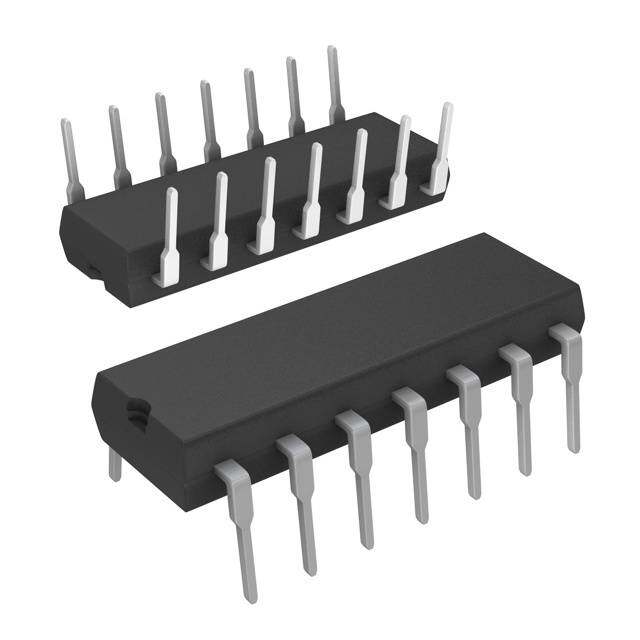
Package information TSZ121, TSZ122, TSZ124 6.7 TSSOP14 package information Figure 58: TSSOP14 package outline aaa Table 12: TSSOP14 mechanical data Dimensions Ref. Millimeters Inches Min. Typ. Max. Min. Typ. Max. A 1.20 0.047 A1 0.05 0.15 0.002 0.004 0.006 A2 0.80 1.00 1.05 0.031 0.039 0.041 b 0.19 0.30 0.007 0.012 c 0.09 0.20 0.004 0.0089 D 4.90 5.00 5.10 0.193 0.197 0.201 E 6.20 6.40 6.60 0.244 0.252 0.260 E1 4.30 4.40 4.50 0.169 0.173 0.176 e 0.65 0.0256 L 0.45 0.60 0.75 0.018 0.024 0.030 L1 1.00 0.039 k 0° 8° 0° 8° aaa 0.10 0.004 32/35 DocID023563 Rev 8
TSZ121, TSZ122, TSZ124 Ordering information 7 Ordering information Table 13: Order codes Order code Temperature range Package Packaging Marking TSZ121ICT SC70-5 K44 TSZ121ILT SΟΤ23-5 K143 TSZ122IQ2T DFN8 2x2 K33 TSZ122IST -40 to 125 °C MiniSO8 K208 TSZ122IDT SO8 TSZ122I TSZ124IQ4T QFN16 3x3 Tape and reel K193 TSZ124IPT TSSOP14 TSZ124I TSZ121IYLT (1) SΟΤ23-5 K192 TSZ122IYDT (1) SO8 K192D -40 to 125 °C automotive grade TSZ122IYST (1) MiniSO8 K192 TSZ124IYPT (1) TSSOP14 TSZ124IY Notes: (1)Qualified and characterized according to AEC Q100 and Q003 or equivalent, advanced screening according to AEC Q001 & Q002 or equivalent. DocID023563 Rev 8 33/35
Revision history TSZ121, TSZ122, TSZ124 8 Revision history Table 14: Document revision history Date Revision Changes 16-Aug-2012 1 Initial release. Added dual and quad products (TSZ122 and TSZ124 respectively) Updated title Added following packages: DFN8 2x2, MiniSO8, QFN16 3x3, TSSOP14 Updated Features Added Benefits and Related products Updated Description Updated Table 1 (Rthja, ESD) 25-Apr-2013 2 Updated Table 3 (Vio, ∆Vio/∆T, CMR, Avd, ICC, en, and Cs) Updated Table 4 (Vio, ∆Vio/∆T, CMR, ICC, en, and Cs) Updated Table 5 (Vio, ∆Vio/∆T, CMR, SVR, EMIRR, ICC, ts, en, and Cs) Updated curves of Section 3: Electrical characteristics Added Section 4.7: Capacitive load Small update Section 4.9: Optimized application recommendation (capacitor) Added Section 4.10: EMI rejection ration (EMIRR) Updated Table 10: Order codes Added SO8 package for commercial part number TSZ122IDT Related products: added hyperlinks for TSV71x and TSV73x products Table 1: updated CDM information Figure 6, Figure 7: updated X-axes titles 11-Sep-2013 3 Figure 12: updated X-axis and Y-axis titles Figure 19: updated title Figure 26: updated X-axis (logarithmic scale) Figure 27 and Figure 28: updated Y-axis titles Table 1: updated ESD information Table 5: added footnote 3 23-May-2014 4 Table 10: Order codes: added automotive qualification footnotes 1 and 2; updated marking of TSZ122IST. Updated disclaimer Updated document layout 09-May-2016 5 Table 13: "Order codes": added new automotive grade order code TSZ122IYD, updated footnotes of other automotive grade order codes. Table 3, Table 4, and Table 5: added parameter "Low-frequency peak-to-peak input 07-Feb-2017 6 noise" (∫en). Figure 26: "0.1 Hz to 10 Hz noise": updated legend (0.75 μVpp instead of 0.2 μVpp) Updated footnote related to TSZ122IYDT in Table 13: "Order codes". Minor changes 12-Apr-2017 7 throughout the document. Updated package outline drawing and mechanical data in Section 6.2: SOT23-5 18-May-2017 8 package information. 34/35 DocID023563 Rev 8
TSZ121, TSZ122, TSZ124 IMPORTANT NOTICE – PLEASE READ CAREFULLY STMicroelectronics NV and its subsidiaries (“ST”) reserve the right to make changes, corrections, enhancements, modifications, and improvements to ST products and/or to this document at any time without notice. Purchasers should obtain the latest relevant information on ST products before placing orders. ST products are sold pursuant to ST’s terms and conditions of sale in place at the time of order acknowledgement. Purchasers are solely responsible for the choice, selection, and use of ST products and ST assumes no liability for application assistance or the design of Purchasers’ products. No license, express or implied, to any intellectual property right is granted by ST herein. Resale of ST products with provisions different from the information set forth herein shall void any warranty granted by ST for such product. ST and the ST logo are trademarks of ST. All other product or service names are the property of their respective owners. Information in this document supersedes and replaces information previously supplied in any prior versions of this document. © 2017 STMicroelectronics – All rights reserved DocID023563 Rev 8 35/35
Mouser Electronics Authorized Distributor Click to View Pricing, Inventory, Delivery & Lifecycle Information: S TMicroelectronics: TSZ121ILT TSZ121ICT TSZ122IQ2T TSZ122IST TSZ124IPT TSZ124IQ4T TSZ122IYST TSZ122IDT TSZ121IYLT TSZ124IYPT TSZ122IYDT