ICGOO在线商城 > 集成电路(IC) > 线性 - 放大器 - 仪表,运算放大器,缓冲器放大器 > TSV854IQ4T

 Datasheet下载
- 型号: TSV854IQ4T
- 制造商: STMicroelectronics
- 库位|库存: xxxx|xxxx
- 要求:
| 数量阶梯 | 香港交货 | 国内含税 |
| +xxxx | $xxxx | ¥xxxx |
查看当月历史价格
查看今年历史价格
TSV854IQ4T产品简介:
ICGOO电子元器件商城为您提供TSV854IQ4T由STMicroelectronics设计生产,在icgoo商城现货销售,并且可以通过原厂、代理商等渠道进行代购。 TSV854IQ4T价格参考。STMicroelectronicsTSV854IQ4T封装/规格:线性 - 放大器 - 仪表,运算放大器,缓冲器放大器, 通用 放大器 4 电路 满摆幅 16-QFN(3x3)。您可以下载TSV854IQ4T参考资料、Datasheet数据手册功能说明书,资料中有TSV854IQ4T 详细功能的应用电路图电压和使用方法及教程。
TSV854IQ4T 是 STMicroelectronics(意法半导体)推出的一款线性放大器,属于仪表、运算放大器和缓冲器放大器类别。以下是其主要应用场景:

 1. 工业自动化与控制
   - TSV854IQ4T 的高精度和低噪声特性使其非常适合用于工业自动化中的信号调理电路。例如,在传感器信号放大中,它可以将微弱的模拟信号放大到适合后续处理的水平。
   - 在过程控制系统中,该器件可用于电流环路信号调节或电压信号放大。

 2. 医疗设备
   - 在医疗领域,TSV854IQ4T 可用于心电图(ECG)、脑电图(EEG)等生物医学信号的放大和处理。其低功耗和高精度特性有助于提高设备的可靠性和测量精度。
   - 它还适用于便携式医疗设备,如血糖仪、脉搏血氧仪等,以延长电池寿命并确保信号质量。

 3. 汽车电子
   - TSV854IQ4T 的宽工作温度范围(-40°C 至 +125°C)和车规级认证使其非常适合汽车应用。例如,在车载信息娱乐系统中,它可以用作音频信号放大器。
   - 此外,它还可用于汽车传感器信号调理,如压力传感器、温度传感器等。

 4. 消费类电子产品
   - 在消费类电子产品中,TSV854IQ4T 可用于音频信号放大、传感器接口和电源管理电路。例如,在智能音箱或耳机放大器中,它能够提供高质量的音频输出。
   - 其小封装尺寸(如 QFN 封装)也使得它非常适合空间受限的应用。

 5. 通信设备
   - 在通信领域,TSV854IQ4T 可用于信号放大和滤波,特别是在低功耗要求的无线通信模块中。
   - 它还可以用于数据采集系统中的信号调理,确保传输信号的稳定性和准确性。

 6. 测试与测量
   - 该放大器具有良好的线性和稳定性,适用于精密测量仪器,如数字万用表、示波器和信号发生器。
   - 在这些应用中,TSV854IQ4T 能够准确地放大和处理输入信号,从而提高测量精度。

总之,TSV854IQ4T 凭借其低功耗、高精度和宽工作温度范围等特点,广泛应用于工业、医疗、汽车、消费电子和通信等领域,为各种信号放大和处理任务提供了可靠的解决方案。
| 参数 | 数值 |
| -3db带宽 | - |
| 产品目录 | 集成电路 (IC)半导体 |
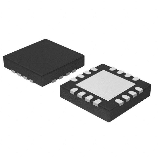
| 描述 | IC OPAMP GP 1.3MHZ RRO 16VFQFPN运算放大器 - 运放 LP 180uA 5V 50nA 0.8V mV 2.5v to 5.5v |
| 产品分类 | Linear - Amplifiers - Instrumentation, OP Amps, Buffer Amps集成电路 - IC |
| 品牌 | STMicroelectronics |
| 产品手册 | |
| 产品图片 |
|
| rohs | 符合RoHS无铅 / 符合限制有害物质指令(RoHS)规范要求 |
| 产品系列 | 放大器 IC,运算放大器 - 运放,STMicroelectronics TSV854IQ4T- |
| 数据手册 | |
| 产品型号 | TSV854IQ4T |
| 产品种类 | 运算放大器 - 运放 |
| 供应商器件封装 | 16-QFN(3x3) |
| 共模抑制比—最小值 | 70 dB |
| 关闭 | No Shutdown |
| 其它名称 | 497-12824-6 |
| 其它有关文件 | http://www.st.com/web/catalog/sense_power/FM123/SC61/SS1613/LN1588/PF251226?referrer=70071840http://www.st.com/web/catalog/sense_power/FM123/SC61/SS1613/LN1604/PF251226?referrer=70071840 |
| 包装 | Digi-Reel® |
| 压摆率 | 0.7 V/µs |
| 商标 | STMicroelectronics |
| 增益带宽生成 | 1.3 MHz |
| 增益带宽积 | 1.3MHz |
| 安装类型 | 表面贴装 |
| 安装风格 | SMD/SMT |
| 封装 | Reel |
| 封装/外壳 | 16-VFQFN 裸露焊盘 |
| 封装/箱体 | QFN-16 |
| 工作温度 | -40°C ~ 125°C |
| 工作电源电压 | 2.5 V to 5.5 V |
| 工厂包装数量 | 3000 |
| 放大器类型 | 通用 |
| 最大工作温度 | + 125 C |
| 最小工作温度 | - 40 C |
| 标准包装 | 1 |
| 电压-电源,单/双 (±) | 2.5 V ~ 5.5 V |
| 电压-输入失调 | 4mV |
| 电流-电源 | 130µA |
| 电流-输入偏置 | 27nA |
| 电流-输出/通道 | 70mA |
| 电源电流 | 120 uA |
| 电路数 | 4 |
| 系列 | TSV854 |
| 转换速度 | 0.6 V/us |
| 输入偏压电流—最大 | 60 nA |
| 输入补偿电压 | 4 mV |
| 输出电流 | 26 mA |
| 输出类型 | 满摆幅 |
| 通道数量 | 4 Channel |


- 商务部:美国ITC正式对集成电路等产品启动337调查
- 曝三星4nm工艺存在良率问题 高通将骁龙8 Gen1或转产台积电
- 太阳诱电将投资9.5亿元在常州建新厂生产MLCC 预计2023年完工
- 英特尔发布欧洲新工厂建设计划 深化IDM 2.0 战略
- 台积电先进制程称霸业界 有大客户加持明年业绩稳了
- 达到5530亿美元!SIA预计今年全球半导体销售额将创下新高
- 英特尔拟将自动驾驶子公司Mobileye上市 估值或超500亿美元
- 三星加码芯片和SET,合并消费电子和移动部门,撤换高东真等 CEO
- 三星电子宣布重大人事变动 还合并消费电子和移动部门
- 海关总署:前11个月进口集成电路产品价值2.52万亿元 增长14.8%


PDF Datasheet 数据手册内容提取
TSV85x, TSV85xA Low-power, high-accuracy, general-purpose operational amplifier Datasheet - production data Related products • See LMV82x series for higher gain bandwidth product (5.5 MHz) SC70-5 SOT23-5 Applications SOT23-6 • Battery-powered applications • Portable devices • Automotive signal conditioning DFN8 2x2 SO8 MiniSO8 • Active filtering MiniSO10 • Medical instrumentation Description The TSV85x, TSV85xA series of single, dual, and SO14 TSSOP14 QFN16 3x3 quad operational amplifiers offer low voltage TSSOP16 operation with a rail-to-rail output swing. The TSV85x, TSV85xA series outperforms the industry standard LMV321, proposing lower Features supply voltage capability, enhanced input offset voltage, and smaller packages. • Low power consumption: 180 µA max at 5 V The devices are offered with either industry • Low power shutdown mode: 50 nA max standard pinouts or with a power-saving • Low offset voltage: 0.8 mV max at 25 °C shutdown feature that reduces the supply current • Tiny packages to a maximum of 50 nA at 25 °C. • Extended temperature range: -40 °C to 125 °C The wide temperature range, high ESD tolerance, and automotive grade qualification ease the use • Low supply voltage: 2.3 V - 5.5 V in harsh automotive applications. • Gain bandwidth product: 1.3 MHz • Automotive qualification Table 1. Device summary Without With Benefits shutdown feature shutdown feature • Longer lifetime in battery-powered applications Standard Enhanced Standard Enhanced • Higher accuracy without calibration Vio Vio Vio Vio • Smaller form factor than equivalent competitor Single TSV851 TSV851A TSV850 TSV850A devices Dual TSV852 TSV852A TSV853 TSV853A • Application performances guaranteed over wide temperature ranges Quad TSV854 TSV854A TSV855 TSV855A April 2017 DocID022468 Rev 4 1/31 This is information on a product in full production. www.st.com
Contents TSV85x, TSV85xA Contents 1 Package pin connections . . . . . . . . . . . . . . . . . . . . . . . . . . . . . . . . . . . . . 3 2 Absolute maximum ratings and operating conditions . . . . . . . . . . . . . 4 3 Electrical characteristics . . . . . . . . . . . . . . . . . . . . . . . . . . . . . . . . . . . . . 6 4 Application information . . . . . . . . . . . . . . . . . . . . . . . . . . . . . . . . . . . . . 14 4.1 Operating voltages . . . . . . . . . . . . . . . . . . . . . . . . . . . . . . . . . . . . . . . . . . 14 4.2 Input common-mode range . . . . . . . . . . . . . . . . . . . . . . . . . . . . . . . . . . . 14 4.3 Rail-to-rail output . . . . . . . . . . . . . . . . . . . . . . . . . . . . . . . . . . . . . . . . . . . 14 4.4 Input offset voltage drift over temperature . . . . . . . . . . . . . . . . . . . . . . . . 14 4.5 PCB layouts . . . . . . . . . . . . . . . . . . . . . . . . . . . . . . . . . . . . . . . . . . . . . . . 14 4.6 Macromodel . . . . . . . . . . . . . . . . . . . . . . . . . . . . . . . . . . . . . . . . . . . . . . . 14 4.7 Shutdown function . . . . . . . . . . . . . . . . . . . . . . . . . . . . . . . . . . . . . . . . . . 15 5 Package information . . . . . . . . . . . . . . . . . . . . . . . . . . . . . . . . . . . . . . . . 16 5.1 SC70-5 (or SOT323-5) package information . . . . . . . . . . . . . . . . . . . . . . 17 5.2 SOT23-5 package information . . . . . . . . . . . . . . . . . . . . . . . . . . . . . . . . . 18 5.3 SOT23-6 package information . . . . . . . . . . . . . . . . . . . . . . . . . . . . . . . . . 19 5.4 DFN8 package information . . . . . . . . . . . . . . . . . . . . . . . . . . . . . . . . . . . . 20 5.5 SO8 package information . . . . . . . . . . . . . . . . . . . . . . . . . . . . . . . . . . . . . 21 5.6 MiniSO8 package information . . . . . . . . . . . . . . . . . . . . . . . . . . . . . . . . . 22 5.7 MiniSO10 package information . . . . . . . . . . . . . . . . . . . . . . . . . . . . . . . . 23 5.8 SO14 package information . . . . . . . . . . . . . . . . . . . . . . . . . . . . . . . . . . . . 24 5.9 TSSOP14 package information . . . . . . . . . . . . . . . . . . . . . . . . . . . . . . . . 25 5.10 TSSOP16 package information . . . . . . . . . . . . . . . . . . . . . . . . . . . . . . . . 26 5.11 QFN16 3x3 package information . . . . . . . . . . . . . . . . . . . . . . . . . . . . . . . 27 6 Ordering information . . . . . . . . . . . . . . . . . . . . . . . . . . . . . . . . . . . . . . . 29 7 Revision history . . . . . . . . . . . . . . . . . . . . . . . . . . . . . . . . . . . . . . . . . . . 30 2/31 DocID022468 Rev 4
TSV85x, TSV85xA Package pin connections 1 Package pin connections Figure 1. Pin connections for each package (top view) In+ 1 5 Vcc+ In+ 11 66 V CC+ ++ Vcc- 2 V 22 __ 5 SHDN CC- In- 3 4 Out In- 33 44 Out SC70-5/SOT23-5 SOT23-6 (cid:50)(cid:56)(cid:55)(cid:20) (cid:20) (cid:27) (cid:57)(cid:38)(cid:38)(cid:14) Out1 1 8 Vcc+ (cid:44)(cid:49)(cid:20)(cid:16) (cid:21) (cid:26) (cid:50)(cid:56)(cid:55)(cid:21) In1- 2 7 Out2 (cid:11)(cid:20)(cid:12) (cid:49)(cid:38) (cid:44)(cid:49)(cid:20)(cid:14) (cid:22) (cid:25) (cid:44)(cid:49)(cid:21)(cid:16) In1+ 3 6 In2- (cid:57)(cid:38)(cid:38)(cid:16) (cid:23) (cid:24) (cid:44)(cid:49)(cid:21)(cid:14) Vcc- 4 5 In2+ DFN8 2x2 SO8/MiniSO8 Out1 1 14 Out4 OOuutt11 11 1100 VV CCCC++ In1- 2 13 In4- IInn11-- 22 __ 99 OOuutt22 In1+ 3 12 In4+ IInn11++ 33 ++ __ 88 IInn22-- Vcc+ 4 11 Vcc- VV 44 ++ 77 IInn22++ In2+ 5 10 In3+ CCCC-- SSSHHHDDDNNN111 55 66 SSSHHHDDDNNN222 In2- 6 9 In3- Out2 7 8 Out3 MiniSO10 SO14/TSSOP14 (cid:20) (cid:23) Out1 1 16 Out4 (cid:20)(cid:16) (cid:56)(cid:55) (cid:56)(cid:55) (cid:23)(cid:16) (cid:49) (cid:50) (cid:50) (cid:49) In1- 2 _ _ 15 In4- (cid:44) (cid:44) (cid:20)(cid:25) (cid:20)(cid:24) (cid:20)(cid:23) (cid:20)(cid:22) In1+ 3 + + 14 In4+ (cid:44)(cid:49)(cid:20)(cid:14) (cid:20) (cid:20)(cid:21) (cid:44)(cid:49)(cid:23)(cid:14) V 4 13 V (cid:57)(cid:38)(cid:38)(cid:14) (cid:21) (cid:20)(cid:20) (cid:57)(cid:38)(cid:38)(cid:16) CC+ CC- (cid:49)(cid:38)(cid:11)(cid:20)(cid:12) In2+ 5 + + 12 In3+ (cid:49)(cid:38) (cid:22) (cid:20)(cid:19) (cid:49)(cid:38) _ _ In2- 6 11 In3- (cid:44)(cid:49)(cid:21)(cid:14) (cid:23) (cid:28) (cid:44)(cid:49)(cid:22)(cid:14) (cid:24) (cid:25) (cid:26) (cid:27) Out2 7 10 Out3 SSHHDDNN11//22 8 9 SSHHDDNN33//44 (cid:44)(cid:49)(cid:21)(cid:16) (cid:50)(cid:56)(cid:55)(cid:21) (cid:50)(cid:56)(cid:55)(cid:22) (cid:44)(cid:49)(cid:22)(cid:16) TSSOP16 QFN16 3x3 1. The exposed pads of the DFN8 2x2 and QFN16 3x3 can be connected to VCC- or left floating. DocID022468 Rev 4 3/31 31
Absolute maximum ratings and operating conditions TSV85x, TSV85xA 2 Absolute maximum ratings and operating conditions Table 2. Absolute maximum ratings (AMR) Symbol Parameter Value Unit V Supply voltage(1) 6 CC V Differential input voltage(2) ±V V id CC V Input pins (IN+ and IN- pins) voltage(3) V - 0.3 to V + 0.3 in cc- cc+ I Input current (4) 10 mA in SHDN Shutdown voltage(5) V - 0.2 to V + 0.2 V CC- CC+ T Storage temperature -65 to +150 °C stg Thermal resistance junction to ambient(6)(7) SC70-5 205 SOT23-5 250 SOT23-6 240 DFN8 2x2 57 SO8 125 R °C/W thja MiniSO8 190 MiniSO10 113 SO14 105 TSSOP14 100 TSSOP16 95 QFN16 3x3 45 T Maximum junction temperature 150 °C j HBM: human body model (except shutdown pin)(8) 4 kV HBM: human body model (shutdown pin)(8) 3.5 ESD MM: machine model(9) 250 V CDM: charged device model(10) 1.3 kV CDM: charged device model TSV855(10) 1 Latch-up immunity 200 mA 1. All voltage values, except differential voltage, are with respect to network ground terminal. 2. The differential voltage is the non-inverting input terminal with respect to the inverting input terminal. 3. VCC-Vin must not exceed 6 V, Vin must not exceed 6 V. 4. Input current must be limited by a resistor in series with the inputs. 5. VCC-Vshdn must not exceed 6 V, Vin must not exceed 6 V. 6. Short-circuits can cause excessive heating and destructive dissipation. 7. R are typical values. th 8. Human body model: 100 pF discharged through a 1.5 kΩ resistor between two pins of the device, done for all couples of pin combinations with other pins floating. 9. Machine model: a 200 pF cap is charged to the specified voltage, then discharged directly between two pins of the device with no external series resistor (internal resistor < 5 Ω), done for all couples of pin combinations with other pins floating. 10. Charged device model: all pins plus package are charged together to the specified voltage and then discharged directly to the ground. 4/31 DocID022468 Rev 4
TSV85x, TSV85xA Absolute maximum ratings and operating conditions Table 3. Operating conditions Symbol Parameter Value Unit V Supply voltage 2.3 to 5.5 CC V V Common mode input voltage range V - 0.2 to V - 1 icm CC- CC+ T Operating free air temperature range -40 to +125 °C oper DocID022468 Rev 4 5/31 31
Electrical characteristics TSV85x, TSV85xA 3 Electrical characteristics Table 4. Ele c trical characteristics at V = 2.7 V with V = 0 V, V = V /2, T = 25 °C, and CC+ CC- icm CC amb R connected to V /2 (unless otherwise specified) L CC Symbol Parameter Conditions Min. Typ. Max. Unit DC performance TSV85xA, T = 25 °C 0.8 TSV85x, T = 25 °C 4 V Input offset voltage mV io TSV85xA, -40°C < T< 125 °C 2 TSV85x, -40 °C < T< 125 °C 6 ΔV /ΔT Input offset voltage drift(1) -40 °C < T< 125 °C 1 μV/°C io T = 25 °C 0.5 30 I Input offset current (V = V /2) io out cc -40°C < T< 125 °C 1 50 nA T = 25 °C 27 60 I Input bias current (V = V /2) ib out cc -40 °C < T< 125 °C 110 Common mode rejection ratio T = 25 °C 70 75 CMR 20 log (ΔV /ΔV ) icm io (Vic = 0 V to Vcc-1V, Vout = Vcc/2) -40 °C < T< 125 °C 68 R = 10 kΩ, T = 25 °C 100 110 L dB Large signal voltage gain RL= 10 kΩ, -40 °C < T< 125 °C 90 A vd (Vout = 0.5V to (Vcc-0.5V)) RL= 2 kΩ, T = 25 °C 90 100 R = 2 kΩ, -40 °C < T< 125 °C 80 L R = 10 kΩ, T = 25 °C 10 100 L R = 10 kΩ, -40 °C < T< 125 °C 200 L V -V High level output voltage CC OH R = 2 kΩ, T = 25 °C 40 300 L R = 2 kΩ, -40 °C < T< 125 °C 400 L mV R = 10 kΩ, T = 25 °C 65 180 L R = 10 kΩ, -40 °C < T< 125 °C 280 L V Low level output voltage OL R = 2 kΩ, T = 25 °C 120 300 L R = 2 kΩ, -40 °C < T< 125 °C 400 L I (V = V ) T = 25 °C 15 26 sink out cc Vid = -1 V -40 °C < T< 125 °C 15 I mA out I (V = 0 V) T = 25 °C 15 21 source out Vid = 1 V -40°C < T< 125°C 12 Supply current (per channel) T = 25°C 120 180 I µA CC No load, V = V /2 out CC -40°C < T< 125°C 180 6/31 DocID022468 Rev 4
TSV85x, TSV85xA Electrical characteristics Table 4. Electrical characteristics at V = 2.7 V with V = 0 V, V = V /2, T = 25 °C, and CC+ CC- icm CC amb R connected to V /2 (unless otherwise specified) (continued) L CC Symbol Parameter Conditions Min. Typ. Max. Unit AC performance GBP Gain bandwidth product 1.3 MHz F Unity gain frequency 1 u R > 1 MΩ, C = 200 pF Φ Phase margin L L 60 degrees m G Gain margin 10 dB m R > 1 MΩ, C = 200 pF SR Slew rate L L 0.6 V/μs V = 0.5 V to V - 0.5V out CC f = 1 kHz 31 en Equivalent input noise voltage f = 10 kHz 20 ---n--H-V---z--- pA i Equivalent input noise current f = 1 kHz 0.30 ------------ n Hz f = 1 kHz, A = 1, in CL R = 10 kΩ, THD+N Total harmonic distortion + noise L 0.002 % Vicm = Vcc/2, BW = 22 kHz, Vout = 1 Vpp 1. See Section 4.4: Input offset voltage drift over temperature. Table 5. Shutdown characteristics V = 2.7 V CC Symbol Parameter Conditions Min. Typ. Max. Unit DC performance SHDN = V 2.5 50 CC- Supply current in shutdown nA I -40 °C < T< 85 °C 200 CC mode (all operators) -40 °C < T< 125 °C 1.5 µA R = 2 kΩ, t Amplifier turn-on time(1) L 300 on V = V to V + 0.2 V out CC- CC - ns R = 2 kΩ, Vout = V - 1 V t Amplifier turn-off time(1) L CC+ 20 off to V - 1.2 V CC+ V - V SHDN logic high CC IH 0.5 V V SHDN logic low 0.5 IL I SHDN current high SHDN = V 10 IH CC+ I SHDN current low SHDN = V 10 pA IL CC- Output leakage in shutdown SHDN = VCC- 50 I OLeak mode -40 °C < T< 125 °C 1 nA 1. See Section 4.7: Shutdown function. DocID022468 Rev 4 7/31 31
Electrical characteristics TSV85x, TSV85xA Table 6. Elec t rical characteristics at V = 5 V with V = 0 V, V = V /2, T = 25 ° C, and R CC+ CC- icm CC amb L connected to V /2 (unless otherwise specified) CC Symbol Parameter Conditions Min. Typ. Max. Unit DC performance TSV85xA, T = 25 °C 0.8 TSV85x, T = 25 °C 4 V Input offset voltage mV io TSV85xA, -40 °C < T< 125 °C 2 TSV85x, -40 °C < T< 125 °C 6 ΔV /ΔT Input offset voltage drift(1) -40 °C < T< 125 °C 1 μV/°C io Input offset current T = 25 °C 0.5 30 I io (Vout = Vcc/2) -40 °C < T< 125 °C 1 50 nA T = 25 °C 27 60 I Input bias current (V = V /2) ib out cc -40 °C < T< 125 °C 110 Common mode rejection ratio T = 25 °C 72 75 CMR 20 log (ΔV /ΔV ) icm io (Vic = 0 V to Vcc-1V, Vout = Vcc/2) -40 °C < T< 125 °C 70 Supply voltage rejection ratio: T = 25 °C 72 79 SVR 20 log (ΔV /ΔV ) cc io V = 2.5 to 5 V -40 °C < T< 125 °C 70 cc dB R = 10 kΩ, T = 25 °C 100 110 L Large signal voltage gain RL= 10 kΩ, -40 °C < T< 125 °C 90 A vd (Vout = 0.5V to (VCC-0.5V)) RL= 2 kΩ, T = 25 °C 90 100 R = 2 kΩ, -40 °C < T< 125 °C 80 L R = 10 kΩ, T=25 °C 10 100 L R = 10 kΩ, -40 °C < T< 125 °C 200 L V -V High level output voltage CC OH R = 2 kΩ, T = 25 °C 40 300 L R = 2 kΩ, -40°C < T< 125 °C 400 L mV R = 10 kΩ, T = 25 °C 65 180 L R = 10 kΩ, -40 °C < T< 125 °C 280 L V Low level output voltage OL R = 2 kΩ, T = 25 °C 120 300 L R = 2 kΩ, -40 °C < T< 125 °C 400 L Isink (Vout = VCC) T = 25 °C 35 43 Vid = -1 V -40 °C < T< 125 °C 25 I mA out I (V = 0 V) T = 25 °C 60 70 source out V = 1 V id -40 °C < T< 125 °C 50 Supply current (per channel) T = 25 °C 130 180 I µA CC No load, V = V /2 out CC -40 °C < T< 125 °C 180 8/31 DocID022468 Rev 4
TSV85x, TSV85xA Electrical characteristics Table 6. Electrical characteristics at V = 5 V with V = 0 V, V = V /2, T = 25 ° C, and R CC+ CC- icm CC amb L connected to V /2 (unless otherwise specified) (continued) CC Symbol Parameter Conditions Min. Typ. Max. Unit AC performance GBP Gain bandwidth product 1.3 MHz F Unity gain frequency 1 u R > 1 MΩ, C = 200 pF Φ Phase margin L L 60 degrees m G Gain margin 10 dB m R > 1 MΩ, C = 200 pF SR Slew rate L L 0.7 V/μs V = 0.5 V to V - 0.5V out CC f = 1 kHz 30 en Equivalent input noise voltage f = 10 kHz 20 ---n--H-V----z-- pA i Equivalent input noise current f = 1 kHz 0.30 ------------ n Hz f = 1 kHz, A = 1, in CL R = 10 kΩ, THD+N Total harmonic distortion + noise L 0.002 % Vicm = Vcc/2, BW = 22 kHz, Vout = 1 Vpp 1. See Section 4.4: Input offset voltage drift over temperature. Table 7. Shutdown characteristics V = 5 V CC Symbol Parameter Conditions Min. Typ. Max. Unit DC performance SHDN = V 2.5 50 CC- Supply current in shutdown nA I -40 °C < T< 85 °C 200 CC mode (per channel) -40 °C < T< 125 °C 1.5 µA R = 2 kΩ, t Amplifier turn-on time(1) L 300 on V = V to V + 0.2 V out CC- CC - ns R = 2 kΩ, Vout = V - 1 V to t Amplifier turn-off time(1) L CC+ 20 off V - 1.2 V CC+ V - V SHDN logic high CC IH 0.5 V V SHDN logic low 0.5 IL I SHDN current high SHDN = V 10 IH CC+ I SHDN current low SHDN = V 10 pA IL CC- Output leakage in shutdown SHDN = VCC- 50 I OLeak mode -40°C < T< 125°C 1 nA 1. See Section 4.7: Shutdown function. DocID022468 Rev 4 9/31 31
Electrical characteristics TSV85x, TSV85xA Figure 2. Supply current vs. supply voltage at Figure 3. Vio distribution at V = 5 V CC V = V /2 icm CC 30 0.20 Vcc=5V T=25°C Vicm=2.5V 25 T=125°C T=25°C 0.15 mA) 20 ent ( n (%) Curr0.10 atio 15 Supply 0.05 T=-40°C Popul 10 5 Vicm=Vcc/2 0.00 2.5 3.0 3.5 4.0 4.5 5.0 5.5 0 -4.0-3.5-3.0-2.5-2.0-1.5-1.0-0.5 0.0 0.5 1.0 1.5 2.0 2.5 3.0 3.5 4.0 Supply Voltage (V) Input offset voltage (mV) Figure 4. Input offset voltage vs. input common Figure 5. Output current vs. output voltage at mode voltage at V = 5 V V = 2.7 V CC CC 30 1.0 Sink 0.9 Vid=-1V 2200 V)0.8 m ut Offset Voltage (00000.....34567 T=125°C T=25°C T=-40°C utput Current (mA) -110000 T=125°CT=125T°=C25°CTV=c2Tc5==°-2C4.07°VC T=-40°C p O n0.2 I --2200 0.1 Vcc=5V Source 0.0 Vid=1V 0.0 0.5 1.0 1.5 2.0 2.5 3.0 3.5 4.0 -30 00..00 0.5 11..00 1.5 22..00 2.5 Input Common Mode Voltage (V) Output Voltage (V) Figure 6. Output current vs. output voltage at Figure 7. Output current vs. supply voltage at V = 5 V V = V /2 CC icm CC 110000 110000 Sink Sink 75 Vid=-1V T=25°C T=-40°C 75 Vid=-1V T=-40°C T=25°C 5500 5500 T=125°C A) A) m 25 m 25 nt ( nt ( urre 00 T=125°C Vcc=5V urre 00 Vicm=Vcc/2 C C put -25 T=125°C T=25°C put -25 ut ut O --5500 O --5500 T=125°C -75 -75 T=25°C Source Source T=-40°C Vid=1V Vid=1V T=-40°C --110000 --110000 00..00 0.5 11..00 1.5 22..00 2.5 33..00 3.5 44..00 4.5 55..00 2.5 33..00 3.5 44..00 4.5 55..00 5.5 Output Voltage (V) Supply Voltage (V) 10/31 DocID022468 Rev 4
TSV85x, TSV85xA Electrical characteristics Figure 8. Voltage gain and phase with Figure 9. Voltage gain and phase with Cl = 100 pF Cl = 200 pF 40 0 40 0 Gain Gain 30 T=25°C -45 30 T=25°C -45 20 -90 20 -90 ain (dB) 10 T=-40°C Phase -135hase (°) ain (dB) 10 T=-40°C Phase -135hase (°) G P G P 0 Vcc=5V -180 0 Vcc=5V -180 Vicm=2.5V Vicm=2.5V Rl=50kΩ Rl=50kΩ -10 Cl=100pF T=125°C -225 -10 Cl=200pF T=125°C -225 Gain=-100 Gain=-100 -20 -270 -20 -270 10k 100k 1M 10M 10k 100k 1M 10M Frequency (Hz) Frequency (Hz) Figure 10. Gain margin vs. load capacitor at Figure 11. Phase margin vs. load capacitor at V = 5 V V = 5 V CC CC 2200 90 18 Rl=600Ω T=25°C 8800 Vcc=5V Vicm=2.5V 1155 70 Rl=600Ω Vload=2.5V n Margin (dB) 1110038 Rl=100TkΩ=125°C se Margin (°) 4456600000 Rl=100kΩ Gai 55 Pha 30 T=-40°C 2200 Vcc=5V T=-40°C 3 Vicm=2.5V 10 T=25°C Vload=2.5V T=125°C 00 00 100 1000 100 1000 Load Capacitor (pF) Load Capacitor (pF) Figure 12. Closed-loop gain in voltage follower Figure 13. Phase margin vs. output current at configuration for different capacitive loads V = 5 V CC 15 80 Vcc=5V Cl=500pF Sink Source Vicm=2.5V 70 1100 Rl=10kΩ T=25°C 60 Cl=100pF Cl=200pF 5 Cl=1000pF n (°) 50 Cl=200pF dB) 00 argi 40 Gain ( -5 hase M 30 Vcc=5V Cl=100pF P 20 Vicm=2.5V Vload=2.5V --1100 Cl=45pF 10 Rl=10KΩ T=25°C -15 0-1.0 -0.8 -0.6 -0.4 -0.2 0.0 0.2 0.4 0.6 0.8 1.0 1k 10k 100k 1M 10M Frequency (Hz) Output Current (mA) DocID022468 Rev 4 11/31 31
Electrical characteristics TSV85x, TSV85xA Figure 14. Positive and negative slew rate vs. Figure 15. Positive slew rate at V = 5 V with CC supply voltage Cl = 100 pF 0.8 22..00 1.5 00..55 11..00 T=-40°C ew rate (V/µs) -0000....3003 TT==112255°C°C T=25°C CRVVilllco==ma12d0k==Ω0VVpcFccc/2/2 put Voltage (V) -0000....0055 T=25°CT=125°C Sl T=25°C T=-40°C Out --11..00 --00..55 T=-40°C Vcc=5V Vicm=Vcc/2 -1.5 Cl=100pF -0.8 Rl=1MΩ --22..00 2.5 33..00 3.5 44..00 4.5 55..00 5.5 -1 0 1 2 3 4 5 6 7 8 9 Supply Voltage (V) Time (µs) Figure 16. Negative slew rate at V = 5 V with Figure 17. Noise vs. frequency CC Cl = 100 pF 22..00 Hz) 140 V Vcc=5V V/ Vicm=Vcc/2 1.5 Vicm=Vcc/2 y (n 112200 T=25°C 11..00 T=-40°C CRll==11M00ΩpF nsit e 100 Output Voltage (V) ---110000......005005 T=25°C T=125°C put Noise Voltage D 4468800000 Vcc=5V Vcc=2.7V n -1.5 ent I 20 al v --22..00 qui 00 -1 0 1 2 3 4 5 6 7 8 9 E 100 1000 10000 Time (µs) Frequency (Hz) Figure 18. 0.1 Hz to 10 Hz noise at V = 5 V Figure 19. Distortion + noise vs. frequency CC 6 10-1 Vcc=5V Vcc=5V 4 VT=ic2m5=°C2.5V BVWin==18V0pkpHz Gain=1 µV) 2 VT=ic2m5=°CVcc/2 Rl=2kΩ e ( %) ois 0 N ( 10-2 oltage n -2 THD + Rl=10kΩ V -4 -6 10-3 0 2 4 6 8 10 100 1000 10000 Time (s) Frequency (Hz) 12/31 DocID022468 Rev 4
TSV85x, TSV85xA Electrical characteristics Figure 20. Distortion + noise vs. output voltage 10-1 Rl=2kΩ 10-2 %) N ( + D H T 10-3 Vcc=5V Gain=1 BW=22kHz Rl=10kΩ Vicm=Vcc/2 T=25°C 10-4 0.01 0.1 1 10 Output Voltage (Vpp) DocID022468 Rev 4 13/31 31
Application information TSV85x, TSV85xA 4 Application information 4.1 Operating voltages The TSV85x, TSV85xA can operate from 2.3 to 5.5 V. The devices’ parameters are fully specified for 2.7 V and 5 V power supplies. Additionally, the main specifications are guaranteed in extended temperature ranges from -40 °C to +125 °C. 4.2 Input common-mode range The TSV85x, TSV85xA has an input common-mode range that includes ground. The input common-mode range is extended from VCC- - 0.2 V to VCC+ - 1 V, with no output phase reversal. 4.3 Rail-to-rail output The operational amplifiers’ output levels can go close to the rails: 180 mV maximum above and below the rail when connected to a 10 kΩ resistive load to V /2. CC 4.4 Input offset voltage drift over temperature The maximum input voltage drift over the temperature variation is defined as follows. ΔVio Vio(T)–Vio(25°C) ---Δ----T------ = max ---------------T-----–-----2---5----°---C----------------- for Tmin < T < Tmax. 4.5 PCB layouts For correct operation, it is advised to add 10 nF decoupling capacitors as close as possible to the power supply pins. 4.6 Macromodel Accurate macromodels of the TSV85x, TSV85xA are available on STMicroelectronics’ web site at www.st.com. These models are a trade-off between accuracy and complexity (that is, time simulation) of the TSV85x, TSV85xA operational amplifiers. They emulate the nominal performances of a typical device within the specified operating conditions mentioned in the datasheet. They also help to validate a design approach and to select the right operational amplifier, but they do not replace on-board measurements. 14/31 DocID022468 Rev 4
TSV85x, TSV85xA Application information 4.7 Shutdown function The operational amplifier is enabled when the SHDN pin is pulled high. To disable the amplifier, the SHDN pin must be pulled down to V . When in shutdown mode, the CC- amplifier output is in a high impedance state. The SHDN pin must never be left floating but tied to V or V . CC+ CC- The turn-on and turn-off times are calculated for an output variation of ±200 mV (Figure 21 and Figure 22 show the test configurations). Figure 23 and Figure 24 show the respective results with these test configurations. Figure 21. Test configuration for turn-on time Figure 22. Test configuration for turn-off time (Vout pulled down) (Vout pulled down) GND GND Vcc Vcc Ω Ω k k 2 2 Vcc –1V + Vcc –1V + - - GND GND Figure 23. Turn-on time, V = 5 V, Figure 24. Turn-off time, V = 5 V, CC CC Vout pulled down, T = 25 °C Vout pulled down, T = 25 °C 3 Shutdown pulse 3 Vcc = 5V T = 25°C 2 V) 2 RL connected to GND e ( V) 1 Vout ag 1 oltage ( 0 put volt 0 Vout V ut O -1 -1 Vcc = 5V T = 25°C -2 Shutdown pulse -2 R connected to GND L -3 -3 -0.1 0.0 0.1 0.2 0.3 0.4 0.5 -0.05 0.00 0.05 0.10 0.15 0.20 Time(µs) Time(µs) DocID022468 Rev 4 15/31 31
Package information TSV85x, TSV85xA 5 Package information In order to meet environmental requirements, ST offers these devices in different grades of ECOPACK® packages, depending on their level of environmental compliance. ECOPACK® specifications, grade definitions and product status are available at: www.st.com. ECOPACK® is an ST trademark. 16/31 DocID022468 Rev 4
TSV85x, TSV85xA Package information 5.1 SC70-5 (or SOT323-5) package information Figure 25. SC70-5 (or SOT323-5) package mechanical drawing SIDE VIEW DIMENSIONS IN MM GAUGE PLANE COPLANAR LEADS SEATING PLANE TOP VIEW Table 8. SC70-5 (or SOT323-5) package mechanical data Dimensions Ref Millimeters Inches Min Typ Max Min Typ Max A 0.80 1.10 0.032 0.043 A1 0.10 0.004 A2 0.80 0.90 1.00 0.032 0.035 0.039 b 0.15 0.30 0.006 0.012 c 0.10 0.22 0.004 0.009 D 1.80 2.00 2.20 0.071 0.079 0.087 E 1.80 2.10 2.40 0.071 0.083 0.094 E1 1.15 1.25 1.35 0.045 0.049 0.053 e 0.65 0.025 e1 1.30 0.051 L 0.26 0.36 0.46 0.010 0.014 0.018 < 0° 8° DocID022468 Rev 4 17/31 31
Package information TSV85x, TSV85xA 5.2 SOT23-5 package information Figure 26. SOT23-5 package mechanical drawing Table 9. SOT23-5 package mechanical data Dimensions Ref. Millimeters Inches Min. Typ. Max. Min. Typ. Max. A 0.90 1.20 1.45 0.035 0.047 0.057 A1 0.15 0.006 A2 0.90 1.05 1.30 0.035 0.041 0.051 B 0.35 0.40 0.50 0.013 0.015 0.019 C 0.09 0.15 0.20 0.003 0.006 0.008 D 2.80 2.90 3.00 0.110 0.114 0.118 D1 1.90 0.075 e 0.95 0.037 E 2.60 2.80 3.00 0.102 0.110 0.118 F 1.50 1.60 1.75 0.059 0.063 0.069 L 0.10 0.35 0.60 0.004 0.013 0.023 K 0 degrees 10 degrees 18/31 DocID022468 Rev 4
TSV85x, TSV85xA Package information 5.3 SOT23-6 package information Figure 27. SOT23-6 package mechanical drawing Table 10. SOT23-6 package mechanical data Dimensions Ref. Millimeters Inches Min. Typ. Max. Min. Typ. Max. A 0.90 1.45 0.035 0.057 A1 0.10 0.004 A2 0.90 1.30 0.035 0.051 b 0.35 0.50 0.013 0.019 c 0.09 0.20 0.003 0.008 D 2.80 3.05 0.110 0.120 E 1.50 1.75 0.060 0.069 e 0.95 0.037 H 2.60 3.00 0.102 0.118 L 0.10 0.60 0.004 0.024 ° 0 ° 10 ° 0 ° 10 ° DocID022468 Rev 4 19/31 31
Package information TSV85x, TSV85xA 5.4 DFN8 package information Figure 28. DFN8 2x2 mm package mechanical drawing (pitch 0.5 mm) Table 11. DFN8 2x2 mm package mechanical data (pitch 0.5 mm) Dimensions Ref. Millimeters Inches Min. Typ. Max. Min. Typ. Max. A 0.51 0.55 0.60 0.020 0.022 0.024 A1 0.05 0.002 A3 0.15 0.006 b 0.18 0.25 0.30 0.007 0.010 0.012 D 1.85 2.00 2.15 0.073 0.079 0.085 D2 1.45 1.60 1.70 0.057 0.063 0.067 E 1.85 2.00 2.15 0.073 0.079 0.085 E2 0.75 0.90 1.00 0.030 0.035 0.040 e 0.50 0.020 L 0.425 0.017 ddd 0.08 0.003 20/31 DocID022468 Rev 4
TSV85x, TSV85xA Package information 5.5 SO8 package information Figure 29. SO8 package mechanical drawing Table 12. SO8 package mechanical data Dimensions Ref. Millimeters Inches Min. Typ. Max. Min. Typ. Max. A 1.75 0.069 A1 0.10 0.25 0.004 0.010 A2 1.25 0.049 b 0.28 0.48 0.011 0.019 c 0.17 0.23 0.007 0.010 D 4.80 4.90 5.00 0.189 0.193 0.197 E 5.80 6.00 6.20 0.228 0.236 0.244 E1 3.80 3.90 4.00 0.150 0.154 0.157 e 1.27 0.050 h 0.25 0.50 0.010 0.020 L 0.40 1.27 0.016 0.050 L1 1.04 0.040 k 1 ° 8 ° 1 ° 8 ° ccc 0.10 0.004 DocID022468 Rev 4 21/31 31
Package information TSV85x, TSV85xA 5.6 MiniSO8 package information Figure 30. MiniSO8 package mechanical drawing Table 13. MiniSO8 package mechanical data Dimensions Ref. Millimeters Inches Min. Typ. Max. Min. Typ. Max. A 1.1 0.043 A1 0 0.15 0 0.006 A2 0.75 0.85 0.95 0.030 0.033 0.037 b 0.22 0.40 0.009 0.016 c 0.08 0.23 0.003 0.009 D 2.80 3.00 3.20 0.11 0.118 0.126 E 4.65 4.90 5.15 0.183 0.193 0.203 E1 2.80 3.00 3.10 0.11 0.118 0.122 e 0.65 0.026 L 0.40 0.60 0.80 0.016 0.024 0.031 L1 0.95 0.037 L2 0.25 0.010 k 0 ° 8 ° 0 ° 8 ° ccc 0.10 0.004 22/31 DocID022468 Rev 4
TSV85x, TSV85xA Package information 5.7 MiniSO10 package information Figure 31. MiniSO10 package mechanical drawing (cid:68)(cid:68)(cid:68) Table 14. MiniSO10 package mechanical data Dimensions Ref. Millimeters Inches Min. Typ. Max. Min. Typ. Max. A 1.10 0.043 A1 0.05 0.10 0.15 0.002 0.004 0.006 A2 0.78 0.86 0.94 0.031 0.034 0.037 b 0.25 0.33 0.40 0.010 0.013 0.016 c 0.15 0.23 0.30 0.006 0.009 0.012 D 2.90 3.00 3.10 0.114 0.118 0.122 E 4.75 4.90 5.05 0.187 0.193 0.199 E1 2.90 3.00 3.10 0.114 0.118 0.122 e 0.50 0.020 L 0.40 0.55 0.70 0.016 0.022 0.028 L1 0.95 0.037 k 0 ° 3 ° 6 ° 0 ° 3 ° 6 ° aaa 0.10 0.004 DocID022468 Rev 4 23/31 31
Package information TSV85x, TSV85xA 5.8 SO14 package information Figure 32. SO14 package mechanical drawing Table 15. SO14 package mechanical data Dimensions Millimeters Inches Ref. Min. Typ. Max. Min. Typ. Max. A 1.35 1.75 0.05 0.068 A1 0.10 0.25 0.004 0.009 A2 1.10 1.65 0.04 0.06 B 0.33 0.51 0.01 0.02 C 0.19 0.25 0.007 0.009 D 8.55 8.75 0.33 0.34 E 3.80 4.0 0.15 0.15 e 1.27 0.05 H 5.80 6.20 0.22 0.24 h 0.25 0.50 0.009 0.02 L 0.40 1.27 0.015 0.05 k 8 ° (max.) ddd 0.10 0.004 24/31 DocID022468 Rev 4
TSV85x, TSV85xA Package information 5.9 TSSOP14 package information Figure 33. TSSOP14 package mechanical drawing (cid:68)(cid:68)(cid:68) Table 16. TSSOP14 package mechanical data Dimensions Ref. Millimeters Inches Min. Typ. Max. Min. Typ. Max. A 1.20 0.047 A1 0.05 0.15 0.002 0.004 0.006 A2 0.80 1.00 1.05 0.031 0.039 0.041 b 0.19 0.30 0.007 0.012 c 0.09 0.20 0.004 0.0089 D 4.90 5.00 5.10 0.193 0.197 0.201 E 6.20 6.40 6.60 0.244 0.252 0.260 E1 4.30 4.40 4.50 0.169 0.173 0.176 e 0.65 0.0256 L 0.45 0.60 0.75 0.018 0.024 0.030 L1 1.00 0.039 k 0° 8° 0° 8° aaa 0.10 0.004 DocID022468 Rev 4 25/31 31
Package information TSV85x, TSV85xA 5.10 TSSOP16 package information Figure 34. TSSOP16 package mechanical drawing (cid:68)(cid:68)(cid:68) b Table 17. TSSOP16 package mechanical data Dimensions Ref. Millimeters Inches Min. Typ. Max. Min. Typ. Max. A 1.20 0.047 A1 0.05 0.15 0.002 0.006 A2 0.80 1.00 1.05 0.031 0.039 0.041 b 0.19 0.30 0.007 0.012 c 0.09 0.20 0.004 0.008 D 4.90 5.00 5.10 0.193 0.197 0.201 E 6.20 6.40 6.60 0.244 0.252 0.260 E1 4.30 4.40 4.50 0.169 0.173 0.177 e 0.65 0.0256 k 0° 8° 0° 8° L 0.45 0.60 0.75 0.018 0.024 0.030 L1 1.00 0.039 aaa 0.10 0.004 26/31 DocID022468 Rev 4
TSV85x, TSV85xA Package information 5.11 QFN16 3x3 package information Figure 35. QFN16 3x3 package mechanical drawing (cid:42)(cid:36)(cid:48)(cid:54)(cid:20)(cid:20)(cid:19)(cid:20)(cid:20)(cid:22)(cid:20)(cid:23)(cid:20)(cid:25)(cid:38)(cid:37) DocID022468 Rev 4 27/31 31
Package information TSV85x, TSV85xA Table 18. QFN16 3x3 mm package mechanical data (pitch 0.5 mm) Dimensions Ref. Millimeters Inches Min. Typ. Max. Min. Typ. Max. A 0.80 0.90 1.00 0.031 0.035 0.039 A1 0 0.05 0 0.002 A3 0.20 0.008 b 0.18 0.30 0.007 0.012 D 2.90 3.00 3.10 0.114 0.118 0.122 D2 1.50 1.80 0.059 0.071 E 2.90 3.00 3.10 0.114 0.118 0.122 E2 1.50 1.80 0.059 0.071 e 0.50 0.020 L 0.30 0.50 0.012 0.020 Figure 36. QFN16 3x3 footprint recommendation (cid:42)(cid:36)(cid:48)(cid:54)(cid:20)(cid:20)(cid:19)(cid:20)(cid:20)(cid:22)(cid:20)(cid:23)(cid:22)(cid:19) 28/31 DocID022468 Rev 4
TSV85x, TSV85xA Ordering information 6 Ordering information Table 19. Order codes for devices without shutdown feature Temperature Order code Package Packing Marking range TSV851ICT SC70-5 K5E TSV851ILT SOT23-5 K153 TSV852IQ2T DFN8 2x2 K5E TSV852IST MiniSO8 K153 TSV852IDT SO8 TSV852I TSV854IPT TSSOP14 TSV854I TSV854IDT SO14 -40 °C to 125 °C Tape and reel TSV854IQ4T QFN16 3x3 K157 TSV851AICT SC70-5 K5F TSV851AILT SOT23-5 K154 TSV852AIST MiniSO8 TSV852AIDT SO8 TSV852AI TSV854AIPT TSSOP14 TSV854AI TSV854AIDT SO14 Table 20. Order codes for devices with shutdown feature Temperature Order code Package Packing Marking range TSV850ILT SOT23-6 K153 TSV853IST MiniSO10 TSV855IPT TSSOP16 TSV855I -40 °C to 125 °C Tape and reel TSV850AILT SOT23-6 K154 TSV853AIST MiniSO10 TSV855AIPT TSSOP16 TSV855AI DocID022468 Rev 4 29/31 31
Revision history TSV85x, TSV85xA Table 21. Order codes (automotive grade parts) Temperature Order code Package Packing Marking range TSV851IYLT SOT23-5 K165 TSV852IYST MiniSO8 TSV852IYDT SO8 TSV852IY TSV854IYPT -40 °C to 125 °C TSSOP14 TSV854IY automotive Tape and reel TSV851AIYLT grade(1) SOT23-5 K166 TSV852AIYST MiniSO8 TSV852AIYDT SO8 TSV852AY TSV854AIYPT TSSOP14 TSV854AIY 1. Qualified and characterized according to AEC Q100 and Q003 or equivalent, advanced screening according to AEC Q001 and Q002 or equivalent. 7 Revision history Table 22. Document revision history Date Revision Changes 10-Nov-2011 1 Initial release. Added QFN16 package with related information. Minimum suplly voltage decreased down to 2.3 V. 06-Jul-2012 2 Modified Figure 2, Figure 7 and Figure 14. Addition of automotive grade parts. Figure 1: Pin connections for each package (top view): added DFN8 2x2 pin connection to show exposed pad; added footnote 1. Section 4.7: Shutdown function: added explanation of Figure 23 and 02-Oct-2013 3 Figure 23. Table 21: Order codes (automotive grade parts): updated footnote 1. Updated disclaimer. Updated Table 11: “L” dimension changed from 0.5 mm to 0.425 mm. 24-Apr-2017 4 Minor text edits throughout the document. 30/31 DocID022468 Rev 4
TSV85x, TSV85xA IMPORTANT NOTICE – PLEASE READ CAREFULLY STMicroelectronics NV and its subsidiaries (“ST”) reserve the right to make changes, corrections, enhancements, modifications, and improvements to ST products and/or to this document at any time without notice. Purchasers should obtain the latest relevant information on ST products before placing orders. ST products are sold pursuant to ST’s terms and conditions of sale in place at the time of order acknowledgement. Purchasers are solely responsible for the choice, selection, and use of ST products and ST assumes no liability for application assistance or the design of Purchasers’ products. No license, express or implied, to any intellectual property right is granted by ST herein. Resale of ST products with provisions different from the information set forth herein shall void any warranty granted by ST for such product. ST and the ST logo are trademarks of ST. All other product or service names are the property of their respective owners. Information in this document supersedes and replaces information previously supplied in any prior versions of this document. © 2017 STMicroelectronics – All rights reserved DocID022468 Rev 4 31/31 31