
 Datasheet下载
- 型号: TSM932CUA+T
- 制造商: TOUCHSTONE
- 库位|库存: xxxx|xxxx
- 要求:
| 数量阶梯 | 香港交货 | 国内含税 |
| +xxxx | $xxxx | ¥xxxx |
查看当月历史价格
查看今年历史价格
TSM932CUA+T产品简介:
ICGOO电子元器件商城为您提供TSM932CUA+T由TOUCHSTONE设计生产,在icgoo商城现货销售,并且可以通过原厂、代理商等渠道进行代购。 TSM932CUA+T价格参考。TOUCHSTONETSM932CUA+T封装/规格:线性 - 比较器, 带电压基准 比较器 CMOS,推挽式,TTL 8-MSOP。您可以下载TSM932CUA+T参考资料、Datasheet数据手册功能说明书,资料中有TSM932CUA+T 详细功能的应用电路图电压和使用方法及教程。
TSM932CUA+T是Touchstone Semiconductor推出的一款低功耗、双路电压比较器,属于线性器件中的比较器类别。该器件采用微型SC-70封装,工作电压范围宽(1.8V至5.5V),具备低传播延迟和微安级静态电流,适用于对功耗和空间要求严苛的便携式电子设备。

其典型应用场景包括:
1. 电池供电设备:如智能手机、可穿戴设备(智能手表、健康监测仪)中用于电池电量检测与低电压报警,凭借其低功耗特性延长设备续航时间。
2. 电源管理电路:在多电压系统中实现电压监控与上电复位功能,确保系统稳定启动与运行。
3. 传感器信号调理:用于将温度、压力、光强等模拟传感器输出的微弱信号与参考电压进行比较,实现数字信号转换,广泛应用于工业控制与物联网终端。
4. 过压/欠压保护电路:在电源模块中实时监测电压异常,触发保护机制,防止后级电路损坏。
5. 消费类电子产品:如无线耳机、便携医疗设备中用于状态检测与信号判断,满足小尺寸和高集成度需求。

TSM932CUA+T凭借其高精度、快速响应和小型化优势,特别适合高密度PCB布局和移动应用场景,是现代低功耗电子系统中理想的电压比较解决方案。
| 参数 | 数值 |
| 产品目录 | 集成电路 (IC) |
| CMRR,PSRR(典型值) | 80dB CMRR,80dB PSRR |
| 描述 | IC COMPARATOR DUAL W/REF 8SMOP |
| 产品分类 | |
| 品牌 | Touchstone Semiconductor |
| 数据手册 | |
| 产品图片 |
|
| 产品型号 | TSM932CUA+T |
| rohs | 无铅 / 符合限制有害物质指令(RoHS)规范要求 |
| 产品系列 | TSM93x |
| 传播延迟(最大值) | 12µs |
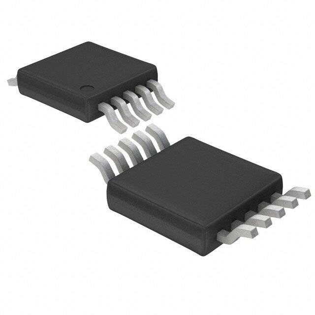
| 供应商器件封装 | 8-MSOP |
| 元件数 | 2 |
| 其它名称 | TSM932CUA+TCT |
| 包装 | 剪切带 (CT) |
| 安装类型 | 表面贴装 |
| 封装/外壳 | 8-TSSOP,8-MSOP(0.118",3.00mm 宽) |
| 工作温度 | 0°C ~ 70°C |
| 标准包装 | 1 |
| 滞后 | 50mV |
| 电压-电源,单/双 (±) | 2.5 V ~ 11 V, ±1.25 V ~ 5.5 V |
| 电压-输入失调(最大值) | 10mV @ 2.5V |
| 电流-输入偏置(最大值) | - |
| 电流-输出(典型值) | 40mA |
| 电流-静态(最大值) | 4.5µA |
| 类型 | 带电压基准 |
| 输出类型 | CMOS,推挽式,TTL |


- 商务部:美国ITC正式对集成电路等产品启动337调查
- 曝三星4nm工艺存在良率问题 高通将骁龙8 Gen1或转产台积电
- 太阳诱电将投资9.5亿元在常州建新厂生产MLCC 预计2023年完工
- 英特尔发布欧洲新工厂建设计划 深化IDM 2.0 战略
- 台积电先进制程称霸业界 有大客户加持明年业绩稳了
- 达到5530亿美元!SIA预计今年全球半导体销售额将创下新高
- 英特尔拟将自动驾驶子公司Mobileye上市 估值或超500亿美元
- 三星加码芯片和SET,合并消费电子和移动部门,撤换高东真等 CEO
- 三星电子宣布重大人事变动 还合并消费电子和移动部门
- 海关总署:前11个月进口集成电路产品价值2.52万亿元 增长14.8%


PDF Datasheet 数据手册内容提取
TSM931-TSM934 Ultra Low-Power Single/Dual-Supply Comparators with Reference FEATURES DESCRIPTION ♦ Alternate source for MAX931-MAX934 The TSM931–TSM934 family of single/dual/quad, ♦ Ultra-Low Quiescent Current Over Temperature low-voltage, micropower analog comparators is TSM931 Single+Reference: 4μA (max) electrically and form-factor identical to the MAX931- TSM932/TSM933 Dual+Reference: 6μA (max) MAX934 family of analog comparators. Ideal for 3V or TSM934 Quad+Reference: 8.5μA (max) 5V single-supply applications, the TSM931–TSM934 ♦ Single or Dual Power Supplies: family can operate from single +2.5V to +11V Single: +2.5V to +11V supplies or from ±1.25V to ±5.5V dual supplies. The Dual: ±1.25V to ±5.5V single TSM931 draws less than 4μA (max) supply ♦ Input Voltage Range Includes Negative Supply current over temperature. The dual TSM932/933 and ♦ 12μs Propagation Delay at 10mV Overdrive the quad TSM934 each draw less than 3μA per ♦ Push-pull TTL/CMOS-Compatible Outputs comparator over temperature. ♦ Crowbar-Current-Free Switching ♦ Continuous Source Current Capability: 40mA All comparators in this family exhibit an input voltage ♦ Internal 1.182V ±2% Reference: range from the negative supply rail to within 1.3V of TSM931/TSM932/TSM933 the positive supply. In addition, the comparators’ ♦ Adjustable Hysteresis: push-pull output stages are TTL/CMOS compatible TSM931/TSM932/TSM933 and capable of sinking and sourcing current. The TSM931/TSM932/TSM933 each incorporates an internal 1.182V ±2% voltage reference. Without APPLICATIONS complicated feedback configurations and only requiring two additional resistors, adding external Threshold Detectors hysteresis via a separate pin is available on the Window Comparator TSM931, the TSM932, and the TSM933. Level Translators Oscillator Circuits Battery-Powered Systems TYPICAL APPLICATION CIRCUIT INTERNAL COMPARATORS INTERNAL PART A 5V, Low-Parts-Count Window Detector REFERENCE PER PACKAGE HYSTERESIS TSM931 Yes 1 Yes TSM932 Yes 2 Yes TSM933 Yes 2 Yes TSM934 Yes 4 No TEMPERATURE PART PACKAGE RANGE TSM931C 0ºC to 70ºC 8-Pin MSOP/SOIC TSM931E -40ºC to 85ºC TSM932C 0ºC to 70ºC 8-Pin MSOP/SOIC TSM932E -40ºC to 85ºC TSM933C 0ºC to 70ºC 8-Pin MSOP/SOIC TSM933E -40ºC to 85ºC TSM934C 0ºC to 70ºC 16-Pin SOIC TSM934E -40ºC to 85ºC Page 1 © 2014 Silicon Laboratories, Inc. All rights reserved.
TSM931-TSM934 ABSOLUTE MAXIMUM RATINGS Supply Voltage (V+ to V-, V+ to GND, GND to V-)......-0.3V, +12V Continuous Power Dissipation (T = +70°C) A Voltage Inputs 8-Pin MSOP (derate 4.1mW/°C above +70°C) .................330mW (IN+, IN-)..............................................(V+ + 0.3V) to (V- - 0.3V) 8-Pin SOIC (derate 5.88mW/°C above +70°C)..................471mW HYST…………………………………….(REF + 5V) to (V- - 0.3V) 16-Pin SOIC (8.7mW/°C above +70°C) ............................696mW Output Voltage Operating Temperature Range REF..................................................... (V+ + 0.3V) to (V- - 0.3V) TSM93xC..................................................................0°C to +70°C OUT (TSM931/934)...........................(V+ + 0.3V) to (GND - 0.3V) TSM93xE...............................................................-40°C to +85°C OUT (TSM932/933)...............................(V+ + 0.3V) to (V- - 0.3V) Storage Temperature Range .................................-65°C to +150°C Input Current (IN+, IN-, HYST)..............................................20mA Lead Temperature (soldering, 10s) ......................................+300°C Output Current REF…………………………………………………………….20mA OUT…………………………………………………………….50mA Output Short-Circuit Duration (V+ ≤ 5.5V) ...................Continuous Electrical and thermal stresses beyond those listed under “Absolute Maximum Ratings” may cause permanent damage to the device. These are stress ratings only and functional operation of the device at these or any other condition beyond those indicated in the operational sections of the specifications is not implied. Exposure to any absolute maximum rating conditions for extended periods may affect device reliability and lifetime. PACKAGE/ORDERING INFORMATION PART PART ORDER NUMBER CARRIER QUANTITY ORDER NUMBER CARRIER QUANTITY MARKING MARKING TSM931CSA+ Tube 97 TSM931CUA+ Tube 50 TS931 Tape TSM931CSA+T 2500 & Reel TAAX TSM931ESA+ Tube 97 Tape TSM931CUA+T 2500 TS931E & Reel Tape TSM931ESA+T 2500 & Reel Page 2 TSM931/34 Rev. 1.0
TSM931-TSM934 PACKAGE/ORDERING INFORMATION PART PART ORDER NUMBER CARRIER QUANTITY ORDER NUMBER CARRIER QUANTITY MARKING MARKING TSM932CSA+ Tube 97 TSM932CUA+ Tube 50 TS932 Tape TSM932CSA+T 2500 & Reel TABD TSM932ESA+ Tube 97 Tape TSM932CUA+T 2500 TS932E & Reel Tape TSM932ESA+T 2500 & Reel PART PART ORDER NUMBER CARRIER QUANTITY ORDER NUMBER CARRIER QUANTITY MARKING MARKING TSM933CSA+ Tube 97 TSM933CUA+ Tube 50 TS933 Tape TSM933CSA+T 2500 & Reel TABB TSM933ESA+ Tube 97 Tape TSM933CUA+T 2500 TS933E & Reel Tape TSM933ESA+T 2500 & Reel TSM931/34 Rev. 1.0 Page 3
TSM931-TSM934 PACKAGE/ORDERING INFORMATION PART ORDER PART ORDER NUMBER CARRIER QUANTITY CARRIER QUANTITY MARKING NUMBER MARKING TSM934CSE+ Tube 48 TSM934ESE+ Tube 48 TS934 TS934E Tape Tape TSM934CSE+T 2500 TSM934ESE+T 2500 & Reel & Reel Lead-free Program: Silicon Labs supplies only lead-free packaging. Consult Silicon Labs for products specified with wider operating temperature ranges. Page 4 TSM931/34 Rev. 1.0
TSM931-TSM934 ELECTRICAL CHARACTERISTICS – 5V OPERATION V+ = 5V, V- = GND = 0V; T = -40ºC to +85ºC, unless otherwise noted. Typical values are at T = +25ºC. See Note 1. A A PARAMETER CONDITIONS MIN TYP MAX UNITS POWER REQUIREMENTS Supply Voltage Range See Note 2 2.5 11 V TSM931; T = +25°C 2.5 3.2 A HYST = REF T = -40°C to +85°C 4 A TSM932 T = +25°C 3.1 4.5 A HYST = REF T = -40°C to +85°C 6 Supply Current IN+ = IN- + 100mV A μA TSM933 T = +25°C 3.1 4.5 A HYST = REF T = -40°C to +85°C 6 A T = +25°C 5.5 6.5 TSM934 A T = -40°C to +85°C 8.5 A COMPARATOR Input Offset Voltage V = 2.5V ±10 mV CM Input Leakage Current (IN-, IN+) IN+ = IN- = 2.5V T = -40°C to +85°C ±0.01 ±5 nA A Input Leakage Current (HYST) TSM931, TSM932, TSM933 ±0.02 nA Input Common-Mode Voltage Range V- V+ – 1.3V V Common-Mode Rejection Ratio V- to (V+ – 1.3V) 0.1 1 mV/V Power-Supply Rejection Ratio V+ = 2.5V to 11V 0.1 1 mV/V Voltage Noise 100Hz to 100kHz 20 μV RMS Hysteresis Input Voltage Range TSM931, TSM932, TSM933 REF- 0.05V REF V Overdrive = 10mV 12 Response Time T = +25°C; 100pF load μs A Overdrive = 100mV 4 Output High Voltage T = -40°C to +85°C: I = 17mA V+ – 0.4 V A OUT T = -40°C to +85°C: TSM932, TSM933 V- + 0.4 V Output Low Voltage A IOUT = 1.8mA TSM931, TSM934 GND + 0.4 V REFERENCE T = 0°C to +70°C 1.158 1.182 1.206 V Reference Voltage A T = -40°C to +85°C 1.147 1.217 V A T = +25°C 15 25 Source Current A μA T = -40°C to +85°C 6 A T = +25°C 8 15 Sink Current A μA T = -40°C to +85°C 4 A Voltage Noise 100Hz to 100kHz 100 μV RMS TSM931/34 Rev. 1.0 Page 5
TSM931-TSM934 ELECTRICAL CHARACTERISTICS – 3V OPERATION V+ = 3V, V- = GND = 0V; T = -40ºC to +85ºC, unless otherwise noted. Typical values are at T = +25ºC. See Note 1. A A PARAMETER CONDITIONS MIN TYP MAX UNITS POWER REQUIREMENTS TSM931; T = +25°C 2.4 3 A HYST = REF T = -40°C to +85°C 3.8 A TSM932 T = +25°C 3.4 4.3 A HYST = REF T = -40°C to +85°C 5.8 Supply Current IN+ = IN- + 100mV A μA TSM933 T = +25°C 3.4 4.3 A HYST = REF T = -40°C to +85°C 5.8 A T = +25°C 5.2 6.2 TSM934 A T = -40°C to +85°C 8 A COMPARATOR Input Offset Voltage V = 1.5V ±10 mV CM Input Leakage Current (IN-, IN+) IN+ = IN- = 1.5V T = -40°C to +85°C ±0.01 ±1 nA A Input Leakage Current (HYST) TSM931, TSM932, TSM933 ±0.02 nA Input Common-Mode Voltage Range V- V+ – 1.3V V Common-Mode Rejection Ratio V- to (V+ – 1.3V) 0.2 1 mV/V Power-Supply Rejection Ratio V+ = 2.5V to 11V 0.1 1 mV/V Voltage Noise 100Hz to 100kHz 20 μV RMS Hysteresis Input Voltage Range TSM931, TSM932, TSM933 REF- 0.05V REF V Overdrive = 10mV 14 Response Time T = +25°C; 100pF load μs A Overdrive = 100mV 5 Output High Voltage T = -40°C to +85°C: I = 10mA V+ – 0.4 V A OUT T = -40°C to +85°C: TSM932, TSM933 V- + 0.4 V Output Low Voltage A IOUT = 0.8mA TSM931, TSM934 GND + 0.4 V REFERENCE T = 0°C to +70°C 1.158 1.182 1.206 V Reference Voltage A T = -40°C to +85°C 1.147 1.217 A T = +25°C 15 25 Source Current A μA T = -40°C to +85°C 6 A T = +25°C 8 15 Sink Current A μA T = -40°C to +85°C 4 A Voltage Noise 100Hz to 100kHz 100 μV RMS Note 1: All specifications are 100% tested at T = +25°C. Specification limits over temperature (T = T to T ) are guaranteed by A A MIN MAX device characterization, not production tested. Note 2: The TSM934 comparator operates below 2.5V. Refer to the “Low-Voltage Operation: V+ = 1.5V (TSM934 Only)” section. Page 6 TSM931/34 Rev. 1.0
TSM931-TSM934 TYPICAL PERFORMANCE CHARA CTERISTICS V = 5V; V = GND; T = +25°C, unless otherwise noted. + - A Output Voltage Low Output Voltage High vs vs Load Current Load Current 2.5 5 V+ = 5V 4.5 V+ = 5V 2 4 1.5 V V+ = 3V V 3.5 V - OL 1 V - OH 3 2.5 V+ = 3V 0.5 2 0 1.5 0 4 8 12 16 20 24 28 0 10 20 30 40 50 LOAD CURRENT - mA LOAD CURRENT - mA Reference Output Voltage vs Reference Voltage vs Temperature Output Load Current 1.190 1.22 V+ = 3V or 5V SINK 1.185 1.21 V V E - 1.180 E - 1.20 AG AG 1.19 LT1.175 LT O O 1.18 V V E 1.170 E C C 1.17 REN1.165 SOURCE REN 1.16 FE FE RE1.160 RE 1.15 1.155 1.14 0 5 10 15 20 25 30 -40 -15 10 35 60 85 LOAD CURRENT - µA TEMPERATURE - ºC TSM931 Supply Current vs TSM932 Supply Current vs Temperature Temperature 4.5 4.5 IN+ = IN- + 100mV IN+ = IN- + 100mV 4 4 A A µ V+ = 5V, V- = -5V µ V+ = 10V, V- = 0V T - 3.5 T - 3.5 N N E E URR 3 URR 3 V+ = 5V, V- = 0V LY C 2.5 V+ = 3V, V- = 0V LY C 2.5 P P P P U U S 2 S 2 V+ = 3V, V- = 0V V+ = 5V, V- = 0V 1.5 1.5 -40 -15 10 35 60 85 -40 -15 10 35 60 85 TEMPERATURE - ºC TEMPERATURE - ºC TSM931/34 Rev. 1.0 Page 7
TSM931-TSM934 TYPICAL PERFORMANCE CHARAC TERISTICS V = 5V; V = GND; T = +25°C, unless otherwise noted. + - A TSM933 Supply Current vs TSM934 Supply Current vs Temperature Temperature 5 10 IN+ = IN- + 100mV 4.5 9 A A NT - µ 4 NT - µ 8 V+ = 5V, V- = -5V E V+ = 5V, V- = 0V E 7 RR3.5 RR V+ = 5V, V- = 0V U U C C 6 Y Y L 3 V+ = 3V, V- = 0V L P P 5 V+ = 3V, V- = 0V P P U U S2.5 S 4 2 3 -40 -15 10 35 60 85 -40 -15 10 35 60 85 TEMPERATURE - ºC TEMPERATURE - ºC TSM934 Supply Current vs Low Supply Voltages Hysteresis Control 10 80 60 OUTPUT HIGH µA 40 NT - V 20 E m URR 1 N- - 0 NO CHANGE Y C + - I -20 PPL IN -40 U S OUTPUT LOW -60 0.1 -80 1.5 2 2.5 0 10 20 30 40 50 SINGLE-SUPPLY VOLTAGE - V V - V - mV REF HYST Transfer Function Response Time vs Load Capacitance 5 18 V- = 0V 16 4 AGE - V 3 ME - µs 1142 VOHL T L TI 10 T VO 2 NSE 8 PU PO VOLH UT 1 ES 6 O R 4 0 2 -0.4 -0.3 -0.2 -0.1 0 0.1 0.2 0.3 0.4 0 20 40 60 80 100 IN+ INPUT VOLTAGE - mV LOAD CAPACITANCE - nF Page 8 TSM931/34 Rev. 1.0
TSM931-TSM934 TYPICAL PERFORMANCE CHARAC TERISTICS V = 5V; V = GND; T = +25°C, unless otherwise noted. + - A Response Time For Various Response Time For Various GE - V Input Overdrives (Low-to-High) GE - V Input Overdrives (High-to-Low) A 5 A 5 VOLT 4 100mV 20mV VOLT 4 50mV 10mV UT 3 UT 3 UTP 2 UTP 2 O O mV 1 50mV 10mV mV 1 100mV 20mV E - 0 E - 0 AG100 AG 100 OLT 0 OLT 0 V V T T U U P -2 0 2 4 6 8 10 12 14 16 18 20 P -2 0 2 4 6 8 10 12 14 16 18 N N I I RESPONSE TIME - µs RESPONSE TIME - µs TSM934 Response Time at TSM934 Source and Sink Current at Low Supply Voltages (Low-to-High) Low Supply Voltages 100 100 SOURCE CURRENT INTO 0.75V LOAD s µ E - ±20mV OVERDRIVE mA TIM10 T - 10 SE EN PON ±100mV OVERDRIVE URR ES C SINK CURRENT AT R VOUT = 0.4V 1 1 1.5 2 2.5 1.5 2 2.5 SINGLE-SUPPLY VOLTAGE - V SINGLE-SUPPLY VOLTAGE - V Short-Circuit Source Current vs Short-Circuit Sink Current vs Supply Voltage Supply Voltage 200 24 OUT CONNECTED TO V+ GND CONNECTED TO V- A 160 T - m mA 22 EN120 T - R OUT CONNECTED TO V- N UR RE 20 C 80 R URCE NK CU 18 O40 SI S 0 16 2 2.5 3 3.5 4 4.5 5 5.5 2 4 6 8 10 TOTAL SUPPLY VOLTAGE - V TOTAL SUPPLY VOLTAGE - V TSM931/34 Rev. 1.0 Page 9
TSM931-TSM934 PIN FUNCTIONS PIN NAME FUNCTION TSM931 TSM932 TSM933 Ground. Connect to V- for single-supply operation. Output swings 1 — — GND from V+ to GND. Comparator A Output. Sinks and sources current. Swings from — 1 1 OUTA V+ to V-. 2 2 2 V- Negative Supply. Connect to ground for single-supply operation. 3 — — IN+ Comparator Noninverting Input — 3 3 INA+ Comparator A Noninverting Input 4 — — IN- Comparator Inverting Input — 4 — INB+ Comparator B Noninverting Input — — 4 INB- Comparator B Inverting Input Hysteresis Input. Connect to REF if not used. Input voltage range 5 5 5 HYST is from V to (V - 50mV). REF REF 6 6 6 REF 1.182V Reference Output with respect to V-. 7 7 7 V+ Positive Supply Voltage Comparator Output. Sinks and sources current. Swings from V+ 8 — — OUT to GND. Comparator B Output. Sinks and sources current. Swings from — 8 8 OUTB V+ to V-. PIN NAME FUNCTION TSM934 Comparator B Output. Sinks and sources current. Swings 1 OUTB from V+ to GND. Comparator A Output. Sinks and sources current. Swings 2 OUTA from V+ to GND. 3 V+ Positive Supply Voltage 4 INA- Comparator A Inverting Input 5 INA+ Comparator A Noninverting Input 6 INB- Comparator B Inverting Input 7 INB+ Comparator B Noninverting Input 8 REF 1.182V Reference Output with respect to V-. Negative Supply Voltage. Connect to ground for single- 9 V- supply operation. 10 INC- Comparator C Inverting Input 11 INC+ Comparator C Noninverting Input 12 IND- Comparator D Inverting Input 13 IND+ Comparator D Noninverting Input 14 GND Ground. Connect to V- for single-supply operation. Comparator D Output. Sinks and sources current. Swings 15 OUTD from V+ to GND. Comparator C Output. Sinks and sources current. Swings 16 OUTC from V+ to GND. Page 10 TSM931/34 Rev. 1.0
TSM931-TSM934 BLOCK DIAGRAMS TSM931/34 Rev. 1.0 Page 11
TSM931-TSM934 THEORY OF OPERATION recommended to evaluate the circuit over the entire power supply range and temperature. The TSM931–TSM934 family of single/dual/quad, Comparator Output low-voltage, micropower analog comparators provide excellent flexibility and performance while The TSM931 and the TSM934 have a GND pin that sourcing continuously up to 40mA of current. The allows the output to swing from V+ to GND while the TSM931-TSM934 provide an on-board 1.182V ±2% V- pin can be set to a voltage below GND as long as reference voltage. To minimize glitches that can the voltage difference between V+ and V- is within occur with parasitic feedback or a less than optimal 11V. Having a different voltage on V- will not affect board layout, the design of the TSM931-TSM934 the output swing. For TTL applications, V+ can be output stage is optimized to eliminate crowbar set to +5V±10% and V- can be set anywhere glitches as the output switches. To minimize current between 0V and -5V±10%. On the other hand, the consumption while providing flexibility, the TSM932 and the TSM933 do not have a GND pin; TSM931-TSM933 have an on-board HYST pin in hence, for TTL applications, V+ needs to be set to a order to add additional hysteresis. +5V power supply and V- to 0V. Furthermore, the output design of the TSM931-TSM934 can source Power-Supply and Input Signal Ranges and sink more than 40mA and 5mA, respectively, while simultaneously maintaining a quiescent current The TSM931-TSM934 can operate from a single in the microampere range. If the power dissipation of supply voltage range of +2.5V to +11V, provide a the package is maintained within the max limit, the wide common mode input voltage range of V- to output can source pulses of 100mA of current with V+-1.3V, and accept input signals ranging from V- to V+ set to +5V. In an effort to minimize external V+ - 1V. The inputs can accept an input as much as component count needed to address power supply 300mV above the below the power supply rails feedback, the TSM931-TSM934 output does not without damage to the part. While the TSM931 and produce crowbar switching current as the output the TSM934 are able to operate from a single supply switches. With a 100mV input overdrive, the voltage range, a GND pin is available that allows for propagation delay of the TSM931-TSM934 is 4μs. a dual supply operation with a range of ±1.25V to ±5.5V. If a single supply operation is desired, the Voltage Reference GND pin needs to be tied to V-. In a dual supply mode, the TSM931 and the TSM934 are compatible The TSM931-TSM934 have an on-board 1.182V with TTL/CMOS with a ±5V voltage and the TSM932 reference voltage with an accuracy of ±2% across a and the TSM933 are compatible with TTL with a temperature range of 0°C to +70°C. The REF pin is single +5V supply. able to source and sink 15μA and 8μA of current, respectively. The REF pin is referenced to V- and it Low-Voltage Operation: V+ = 1.5V (TSM934 Only) should not be bypassed. Due to a decrease in propagation delay and a Noise Considerations reduction in output drive, the TSM931-TSM933 cannot be used with a supply voltage much lower Noise can play a role in the overall performance of than 2.5V. However, the TSM934 can operate down the TSM931-TSM934. Despite having a large gain, if to a supply voltage of 2V; however, as the supply the input voltage is near or equal to the input offset voltage reduces, the TSM934 supply current drops voltage, the output will randomly switch HIGH and and the performance is degraded. When the supply LOW. As a result, the TSM931-TSM934 produces a voltage drops to 2.2V, the reference voltage will no peak-to-peak noise of about 0.3mV while the PP longer function; however, the comparators will reference voltage produces a peak-to-peak noise of function down to a 1.5V supply voltage. about 1mV . Furthermore, it is important to design PP Furthermore, the input voltage range is extended to a layout that minimizes capacitive coupling from a just below 1V the positive supply rail. For given output to the reference pin as crosstalk can applications with a sub-2.5V power supply, it is add noise and as a result, degrade performance. Page 12 TSM931/34 Rev. 1.0
TSM931-TSM934 APPLICATIONS INFORMATION Hysteresis As a result of circuit noise or unintended parasitic feedback, many analog comparators often break into oscillation within their linear region of operation especially when the applied differential input voltage approaches 0V (zero volt). Externally-introduced hysteresis is a well-established technique to stabilizing analog comparator behavior and requires external components. As shown in Figure 1, adding comparator hysteresis creates two trip points: VTHR (for the rising input voltage) and V (for the falling THF input voltage). The hysteresis band (VHB) is defined Figure 2. Programming the HYST Pin as the voltage difference between the two trip points. can accept a voltage between REF and REF-50mV, When a comparator’s input voltages are equal, where a voltage of REF-50mV generates the hysteresis effectively forces one comparator input to maximum voltage across R1 and thus, the maximum move quickly past the other input, moving the input hysteresis and hysteresis band of 50mV and out of the region where oscillation occurs. Figure 1 100mV, respectively. To design the circuit for a illustrates the case in which an IN- input is a fixed desired hysteresis band, consider the equations voltage and an IN+ is varied. If the input signals below to acquire the values for resistors R1 and R2: were reversed, the figure would be the same with an inverted output. V HB R1 = (cid:4666)2 x I (cid:4667) REF V 1.182 - HB 2 R2 = I REF where I is the primary source of current out of the REF reference pin and should be maintained within the maximum current the reference can source. This is typically in the range of 0.1μA and 4μA. It is also important to ensure that the current from reference is much larger than the HYST pin input current. Given R2 = 2.4MΩ, the current sourced by the reference is Figure 1. Threshold Hysteresis Band 0.5μA. This allows the hysteresis band and R1 to be approximated as follows: Hysteresis (TSM931-TSM933) R1(kΩ) = VHB(mv) Hysteresis can be generated with two external For the TSM932-TSM933, the hysteresis is the resistors using positive feedback as shown in same for both comparators. Figure 2. Resistor R1 is connected between REF and HYST and R2 is connected between HYST and Hysteresis (TSM934) V-. This will increase the trip point for the rising input voltage, V , and decrease the trip point for the Relative to adding hysteresis with the HYST pin as THR falling input voltage, V , by the same amount. If no was done for the TSM931-TSM933, the circuit in THF hysteresis is required, connect HYST to REF. The Figure 3 uses positive feedback along with two hysteresis band, V , is voltage across the REF and external resistors to set the desired hysteresis. The HB HYST pin multiplied by a factor of 2. The HYST pin circuit consumes more current and it slows down the hysteresis effect due to the high impedance on the TSM931/34 Rev. 1.0 Page 13
TSM931-TSM934 1 R2 = V 1 1 (cid:3428)(cid:3436) THR (cid:3440)- - (cid:3432) V x R1 R1 R3 REF 1 = 3 1 1 (cid:3428)(cid:3436) (cid:3440)- - (cid:3432) 1.182V x 100kΩ 100kΩ 10MΩ = 65.44kΩ In this example, a 64.9kΩ, 1% standard value resistor is selected for R2. 6. The last step is to verify the trip voltages and hysteresis band using the standard Figure 3. External Hysteresis resistance values: feedback. The following procedure explains the steps to design the circuit for a desired hysteresis: 1 1 1 V = V x R1 x (cid:3436) + + (cid:3440) THR REF R1 R2 R3 1. Choosing R3. As the leakage current at the IN+ pin is less than 1nA, the current through (cid:4666)R1 x V+(cid:4667) V = V – R3 should be at least 100nA to minimize THF THR R3 offset voltage errors caused by the input leakage current. For R3 = 11.8MΩ, the Board Layout and Bypassing current through R3 is V /R3 at the trip REF point. In this case, a 10MΩ resistor is a good While power-supply bypass capacitors are not standard value for R3. typically required, it is good engineering practice to use 0.1μF bypass capacitors close to the device’s 2. Next, the desired hysteresis band ( V ) is power supply pins when the power supply HB set. In this example, V is set to 50mV. impedance is high, the power supply leads are long, HB or there is excessive noise on the power supply 3. Calculating R1. traces. To reduce stray capacitance, it is also good engineering practice to make signal trace lengths as V short as possible. Also recommended are a ground HB R1 = R3 x plane and surface mount resistors and capacitors. V+ 50mV TYPICAL APPLICATION CIRCUITS = 10MΩ x 5V Auto-Off Power Source = 100kΩ A timed auto power-off circuit can be designed as In this example, a 100kΩ, 1% standard shown in Figure 4 where the output of the TSM931 value resistor is selected for R1. is the switched power-supply output. With an internal reference, hysteresis, high current output, and a 2.5 4. Choose the trip point for V rising (V ), IN THR μA supply current, the TSM931 provides a wealth of which is the threshold voltage at which the features that make it perfect for this application. comparator switches its output from low to While consuming only 3.5μA of quiescent current high as V rises above the trip point. In this IN with a 10mA load, the TSM931 is able to generate a example, choose V = 3V. THR voltage of VBATT – 0.12V. As shown in the figure, three resistors are used to generate a hysteresis 5. Calculating R2. band of 100mV and sets the IN+ trip point to 50mV when IN+ is going low. The maximum power-on period of the OUT pin before power-down occurs Page 14 TSM931/34 Rev. 1.0
TSM931-TSM934 respectively. If both OUTA and OUTB signals are ANDed together, the resulting output of the AND gate is an active-high, power-good signal. To design the circuit, the following procedure needs to be performed: 1. As described in the section “Hysteresis (TSM931-TSM933)”, determine the desired hysteresis and select resistors R4 and R5 accordingly. This circuit has ±5mV of hysteresis at the input where the input voltage V will appear larger due to the IN input resistor divider. 2. Selecting R1. As the leakage current at the Figure 4. Auto-Off Power Switch Operates on 2.5µA quiescent current. INB- pin is less than 1nA, the current through R1 should be at least 100nA to can be determined by the RC time constant as minimize offset voltage errors caused by the follows: input leakage current. Values within 100kΩ and 1MΩ are recommended. In this R x C X 4.6 s example, a 294kΩ, 1% standard value resistor is selected for R1. The period value will change depending on the leakage current and the voltage applied to the 3. Calculating R2 + R3. As the input voltage circuit. For instance: 2MΩ x 10μF x 4.6 s = 92 s. V rises, the overvoltage threshold should IN be 5.5V. Choose R2 + R3 as follows: Window Detector V OTH R2 + R3 = R1 x (cid:3436) - 1(cid:3440) The schematic shown in Figure 5 is for a 4.5V V +V REF HYS undervoltage threshold detector and a 5.5V overvoltage threshold detector using the TSM933. 5.5V Resistor components R1, R2, and R3 can be = 294kΩ x (cid:3436) - 1(cid:3440) 1.182V +5mV = 1.068MΩ 4. Calculating R2. As the input voltage VIN falls, the undervoltage threshold should be 4.5V. Choose R2 as follows: (cid:4666)V -V (cid:4667) REF HYS R2 = (R1 + R2+ R3) x - 294k V UTH (cid:4666)1.182V-5mV(cid:4667) = (294kΩ + 1.068MΩ) x - 294k 4.5 Figure 5. Window Detector = 62.2kΩ selected based on the threshold voltage desired In this example, a 61.9kΩ, 1% standard while resistors R4 and R5 can be selected based on value resistor is selected for R2. the hysteresis desired. Adding hysteresis to the circuit will minimize chattering on the output when 5. Calculating R3. the input voltage is close to the trip point. OUTA and OUTB generate the active low undervoltage R3 = (R2 + R3) - R2 indication and active-low overvoltage indication, TSM931/34 Rev. 1.0 Page 15
TSM931-TSM934 = 1.068MΩ – 61.9kΩ Bar-Graph Level Gauge = 1.006MΩ A simple four-stage level detector is shown in Figure 6 using the TSM934. Due to its high output In this example, a 1MΩ, 1% standard value source capability, the TSM921 is perfect for driving resistor is selected for R3. LEDs. When all of the LEDs are on, the threshold voltage is given as VIN =(R1 + R2)/R1 volts. All other 6. Using the equations below, verify all resistor threshold voltages are scaled down accordingly by values selected: ¾, ½, and ¼ the threshold voltage. The current (cid:4666)R1 + R2 + R3(cid:4667) through the LEDs is limited by the output resistors. V = (V + V ) x OTH REF HYS R1 Level Shifter = 5.474V Figure 7 provides a simple way to shift from bipolar (cid:4666)R1 + R2 + R3(cid:4667) ±5V inputs to TTL signals by using the TSM934. To V = (V - V ) x OTH REF HYS (R1+R2) protect the comparator inputs, 10kΩ resistors are placed in series and do not have an effect on the = 4.484V performance of the circuit. Where the hysteresis voltage is given by: Two-Stage Low-Voltage Detector R5 V = V x A two step, input voltage monitoring circuit can be HYS REF R4 designed using the TSM932 as shown in Figure 8. In this circuit, when V is above the LOW and FAIL IN thresholds, the outputs will be HIGH. The design procedure used to design the window detector can be used to design this circuit. Figure 6. Bar-Graph Level Gauge Figure 7. Level Shifter: ±5V Input into CMOS output Page 16 TSM931/34 Rev. 1.0
TSM931-TSM934 Figure 8. Two-Stage Low-Voltage Detector TSM931/34 Rev. 1.0 Page 17
TSM931-TSM934 PACKAGE OUTLINE DRAWING 8-Pin SOIC Package Outline Drawing (N.B., Drawings are not to scale) 0.33 -0.51 0.546 REF 5.80 –6.20 1.27 TYP LEADFARME 3.73 -3.89 2 4.80 -5.00 1 THICKNESS 1.32 –1.52 0.19 –0.25 0.48 Max 0.76 Max 7' REF ALL SIDE 7' REF 0.28 Min 0.66 Min ALL SIDE 45' Angle 1.75 Max GAUGE PLANE 3.81 –3.99 0.25 0.10 –0.25 2 0 -8° 0.406 –0.863 Notes: 0.10 Max 1 Does not include mold flash, protrusions or gate burns. Mold flash, protrusions or gate burrs shall not exceed 0.15 mm per side. 2 Does not include inter-lead flash or protrusions. Inter-lead flash or protrusions shall not exceed 0.25 mm per side. 3. Lead span/stand off height/coplanarity are considered as special characteristic (s). 4. Controlling dimensions are in mm. 5. This part is compliant with JEDEC specification MS-012 6. Lead span/stand off height/coplanarity are considered as Special characteristic. Page 18 TSM931/34 Rev. 1.0
TSM931-TSM934 PACKAGE OUTLINE DRAWING 8-Pin MSOP Package Outline Drawing (N.B., Drawings are not to scale) TSM931/34 Rev. 1.0 Page 19
TSM931-TSM934 PACKAGE OUTLINE DRAWING 16-Pin SOIC Package Outline Drawing (N.B., Drawings are not to scale) Patent Notice Silicon Labs invests in research and development to help our customers differentiate in the market with innovative low-power, small size, analog-intensive mixed-signal solutions. Silicon Labs' extensive patent portfolio is a testament to our unique approach and world-class engineering team. The information in this document is believed to be accurate in all respects at the time of publication but is subject to change without notice. Silicon Laboratories assumes no responsibility for errors and omissions, and disclaims responsibility for any consequences resulting from the use of information included herein. Additionally, Silicon Laboratories assumes no responsibility for the functioning of undescribed features or parameters. Silicon Laboratories reserves the right to make changes without further notice. Silicon Laboratories makes no warranty, representation or guarantee regarding the suitability of its products for any particular purpose, nor does Silicon Laboratories assume any liability arising out of the application or use of any product or circuit, and specifically disclaims any and all liability, including without limitation consequential or incidental damages. Silicon Laboratories products are not designed, intended, or authorized for use in applications intended to support or sustain life, or for any other application in which the failure of the Silicon Laboratories product could create a situation where personal injury or death may occur. Should Buyer purchase or use Silicon Laboratories products for any such unintended or unauthorized application, Buyer shall indemnify and hold Silicon Laboratories harmless against all claims and damages. Silicon Laboratories and Silicon Labs are trademarks of Silicon Laboratories Inc. Other products or brandnames mentioned herein are trademarks or registered trademarks of their respective holders. Page 20 Silicon Laboratories, Inc. TSM931/34 Rev. 1.0 400 West Cesar Chavez, Austin, TX 78701 +1 (512) 416-8500 ▪ www.silabs.com
Smart. Connected. Energy-Friendly Products Quality Support and Community www.silabs.com/products www.silabs.com/quality community.silabs.com Disclaimer Silicon Laboratories intends to provide customers with the latest, accurate, and in-depth documentation of all peripherals and modules available for system and software implementers using or intending to use the Silicon Laboratories products. Characterization data, available modules and peripherals, memory sizes and memory addresses refer to each specific device, and "Typical" parameters provided can and do vary in different applications. Application examples described herein are for illustrative purposes only. Silicon Laboratories reserves the right to make changes without further notice and limitation to product information, specifications, and descriptions herein, and does not give warranties as to the accuracy or completeness of the included information. Silicon Laboratories shall have no liability for the consequences of use of the information supplied herein. This document does not imply or express copyright licenses granted hereunder to design or fabricate any integrated circuits. The products must not be used within any Life Support System without the specific written consent of Silicon Laboratories. A "Life Support System" is any product or system intended to support or sustain life and/or health, which, if it fails, can be reasonably expected to result in significant personal injury or death. Silicon Laboratories products are generally not intended for military applications. Silicon Laboratories products shall under no circumstances be used in weapons of mass destruction including (but not limited to) nuclear, biological or chemical weapons, or missiles capable of delivering such weapons. Trademark Information Silicon Laboratories Inc., Silicon Laboratories, Silicon Labs, SiLabs and the Silicon Labs logo, CMEMS®, EFM, EFM32, EFR, Energy Micro, Energy Micro logo and combinations thereof, "the world’s most energy friendly microcontrollers", Ember®, EZLink®, EZMac®, EZRadio®, EZRadioPRO®, DSPLL®, ISOmodem ®, Precision32®, ProSLIC®, SiPHY®, USBXpress® and others are trademarks or registered trademarks of Silicon Laboratories Inc. ARM, CORTEX, Cortex-M3 and THUMB are trademarks or registered trademarks of ARM Holdings. Keil is a registered trademark of ARM Limited. All other products or brand names mentioned herein are trademarks of their respective holders. Silicon Laboratories Inc. 400 West Cesar Chavez Austin, TX 78701 USA http://www.silabs.com