ICGOO在线商城 > 集成电路(IC) > 接口 - 驱动器,接收器,收发器 > TSB41AB3PFP

 Datasheet下载
- 型号: TSB41AB3PFP
- 制造商: Texas Instruments
- 库位|库存: xxxx|xxxx
- 要求:
| 数量阶梯 | 香港交货 | 国内含税 |
| +xxxx | $xxxx | ¥xxxx |
查看当月历史价格
查看今年历史价格
TSB41AB3PFP产品简介:
ICGOO电子元器件商城为您提供TSB41AB3PFP由Texas Instruments设计生产,在icgoo商城现货销售,并且可以通过原厂、代理商等渠道进行代购。 TSB41AB3PFP价格参考¥25.84-¥48.00。Texas InstrumentsTSB41AB3PFP封装/规格:接口 - 驱动器,接收器,收发器, 半 收发器 6/6 IEEE 1394 80-HTQFP(12x12)。您可以下载TSB41AB3PFP参考资料、Datasheet数据手册功能说明书,资料中有TSB41AB3PFP 详细功能的应用电路图电压和使用方法及教程。
TSB41AB3PFP 是由 Texas Instruments(德州仪器)生产的一款接口驱动器、接收器和收发器。该型号主要应用于高速数据传输和信号调理领域,以下是其典型应用场景:

 1. 工业自动化
   - 在工业控制中,TSB41AB3PFP 可用于实现设备之间的高速通信,例如 PLC(可编程逻辑控制器)、传感器和执行器之间的数据交换。
   - 它支持 RS-485 和 RS-422 标准,适用于长距离、多点通信网络,能够有效减少电磁干扰 (EMI),确保工业环境下的稳定信号传输。

 2. 通信设备
   - 该芯片常用于通信基础设施中的数据链路层,例如路由器、交换机和调制解调器等设备。
   - 其高抗噪能力和低功耗特性使其成为构建可靠通信链路的理想选择。

 3. 汽车电子
   - 在汽车行业中,TSB41AB3PFP 可用于车载网络系统,例如 CAN 总线的辅助通信模块。
   - 它支持差分信号传输,适合复杂的车内电气环境,确保信号完整性并降低噪声影响。

 4. 消费电子产品
   - 在家用或商用消费类设备中,如打印机、扫描仪和 POS 终端,TSB41AB3PFP 提供了高效的接口解决方案。
   - 它可以将短距离信号转换为适合长距离传输的差分信号,增强设备间的互操作性。

 5. 医疗设备
   - 医疗设备需要高精度和高可靠性的数据传输,TSB41AB3PFP 的高性能和低误码率特性非常适合此类应用。
   - 例如,在监护仪、超声设备和其他需要实时数据传输的医疗仪器中,该芯片可用于内部或外部通信模块。

 6. 楼宇自动化
   - 在智能建筑系统中,TSB41AB3PFP 能够连接 HVAC(暖通空调)、照明控制系统和安防设备,支持高效的数据采集与监控。

 特性总结:
- 支持 RS-485/RS-422 差分通信协议。
- 高速数据传输速率(最高可达 10 Mbps)。
- 强大的 ESD 保护能力。
- 工作温度范围广(-40°C 至 +85°C),适应各种严苛环境。

综上所述,TSB41AB3PFP 广泛应用于需要高速、可靠和抗干扰能力强的通信场景,特别适合工业、通信、汽车和医疗等领域。
| 参数 | 数值 |
| 产品目录 | 集成电路 (IC)半导体 |
| 描述 | IC CABLE XCVR/ARBITER 80HTQFP1394 接口集成电路 Three-Port Cable Xcvr/Arbiter |
| 产品分类 | |
| 品牌 | Texas Instruments |
| 产品手册 | |
| 产品图片 |
|
| rohs | 符合RoHS无铅 / 符合限制有害物质指令(RoHS)规范要求 |
| 产品系列 | 1394 接口集成电路,Texas Instruments TSB41AB3PFP- |
| 数据手册 | |
| 产品型号 | TSB41AB3PFP |
| PCN组件/产地 | |
| 产品 | 1394a |
| 产品目录页面 | |
| 产品种类 | 1394 接口集成电路 |
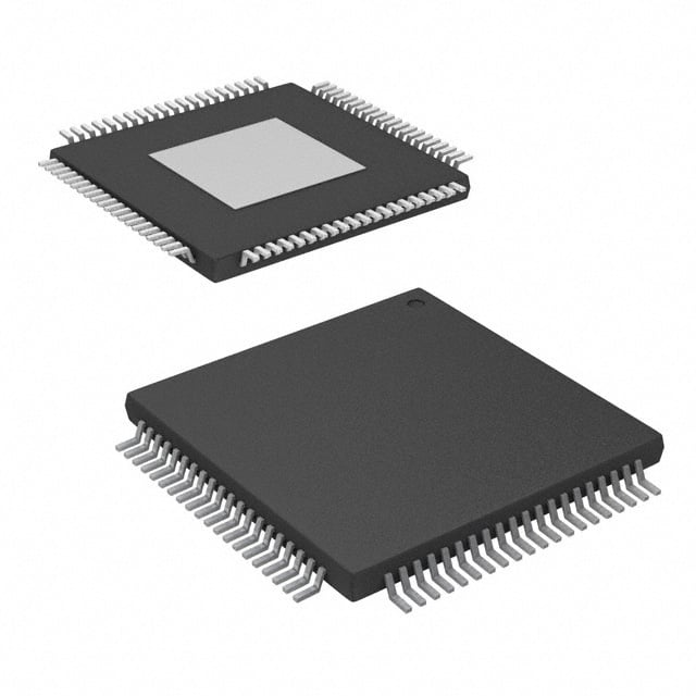
| 供应商器件封装 | 80-HTQFP(12x12) |
| 其它名称 | 296-11077 |
| 包装 | 托盘 |
| 协议 | IEEE 1394 |
| 单位重量 | 368.100 mg |
| 双工 | 半 |
| 商标 | Texas Instruments |
| 安装类型 | 表面贴装 |
| 安装风格 | SMD/SMT |
| 封装 | Tray |
| 封装/外壳 | 80-TQFP 裸露焊盘 |
| 封装/箱体 | HTQFP-80 |
| 工作温度 | 0°C ~ 70°C |
| 工作温度范围 | 0 C to + 70 C |
| 工作电源电压 | 3.3 V |
| 工厂包装数量 | 96 |
| 接收器滞后 | - |
| 描述/功能 | IEEE 1394A THREE-PORT CABLE TRANSCEIVER/ARBITER |
| 数据速率 | - |
| 标准包装 | 96 |
| 电压-电源 | 3 V ~ 3.6 V |
| 电源电流 | 115 mA |
| 类型 | 收发器 |
| 系列 | TSB41AB3 |
| 驱动器/接收器数 | 6/6 |


- 商务部:美国ITC正式对集成电路等产品启动337调查
- 曝三星4nm工艺存在良率问题 高通将骁龙8 Gen1或转产台积电
- 太阳诱电将投资9.5亿元在常州建新厂生产MLCC 预计2023年完工
- 英特尔发布欧洲新工厂建设计划 深化IDM 2.0 战略
- 台积电先进制程称霸业界 有大客户加持明年业绩稳了
- 达到5530亿美元!SIA预计今年全球半导体销售额将创下新高
- 英特尔拟将自动驾驶子公司Mobileye上市 估值或超500亿美元
- 三星加码芯片和SET,合并消费电子和移动部门,撤换高东真等 CEO
- 三星电子宣布重大人事变动 还合并消费电子和移动部门
- 海关总署:前11个月进口集成电路产品价值2.52万亿元 增长14.8%


PDF Datasheet 数据手册内容提取
(cid:1)(cid:2)(cid:3)(cid:4)(cid:5)(cid:6)(cid:3)(cid:7) (cid:8)(cid:9)(cid:9)(cid:9) (cid:5)(cid:7)(cid:10)(cid:4)(cid:11)(cid:12)(cid:13)(cid:14)(cid:14)(cid:14) (cid:1)(cid:15)(cid:16)(cid:9)(cid:9)(cid:12)(cid:17)(cid:18)(cid:16)(cid:1) (cid:19)(cid:6)(cid:3)(cid:20)(cid:9) (cid:1)(cid:16)(cid:6)(cid:21)(cid:2)(cid:19)(cid:9)(cid:8)(cid:22)(cid:9)(cid:16)(cid:23)(cid:6)(cid:16)(cid:3)(cid:8)(cid:1)(cid:9)(cid:16) SLLS418I − JUNE 2000 − REVISED DECEMBER 2004 (cid:1) (cid:1) Fully Supports Provisions of IEEE Data Interface to Link-Layer Controller 1394-1995 Standard for High Performance Through 2/4/8 Parallel Lines at 49.152 MHz Serial Bus† and the 1394a-2000 Supplement (cid:1) Interface to Link Layer Controller Supports (cid:1) Fully Interoperable With FireWire and Low-Cost TI Bus-Holder Isolation and i.LINK Implementation of IEEE Std 1394 Optional Annex J Electrical Isolation (cid:1) (cid:1) Fully Compliant With Open HCI Interoperable With Link-Layer Controllers Requirements Using 3.3-V and 5-V Supplies (cid:1) (cid:1) Provides Three 1394a-2000 Fully Compliant Interoperable With Other Physical Layers Cable Ports at 100/200/400 Megabits Per (PHYs) Using 3.3-V and 5-V Supplies Second (Mbits/s) (cid:1) Low-Cost 24.576-MHz Crystal Provides (cid:1) Full 1394a-2000 Support Includes: Transmit Receive Data at 100/200/400 Connection Debounce, Arbitrated Short Mbits/s, and Link-Layer Controller Clock at Reset, Multispeed Concatenation, 49.152 MHz. Arbitration Acceleration, Fly-By (cid:1) Separate Cable Bias (TPBIAS) for Each Port Concatenation, Port (cid:1) Single 3.3-V Supply Operation Disable/Suspend/Resume (cid:1) (cid:1) Low-Cost High Performance 80-Pin TQFP Extended Resume Signaling for (PFP) Thermally Enhanced Package Compatibility With Legacy DV Devices (cid:1) (cid:1) Direct Drop-In Upgrade for Power-Down Features to Conserve Energy TSB41LV03APFP and TSB41LV03PFP in Battery Powered Applications Include: (cid:1) Software Device Reset (SWR) Automatic Device Power Down During (cid:1) Suspend, Device Power-Down Terminal, Fail-Safe Circuitry Senses Sudden Loss of Link Interface Disable via LPS, and Inactive Power to the Device and Disables the Ports Ports Powered Down to Ensure That the TSB41AB3 Does Not (cid:1) Load the TPBIAS of Any Connected Device Ultralow-Power Sleep Mode (cid:1) and Blocks Any Leakage From the Port Node Power Class Information Signaling Back to Power Plane. for System Power Management (cid:1) (cid:1) The TSB41AB3 Has a 1394a-Compliant Cable Power Presence Monitoring Common-Mode Noise Filter on the (cid:1) Cable Ports Monitor Line Conditions for Incoming Bias Detect Circuit to Filter Out Active Connection to Remote Node. Crosstalk Noise. (cid:1) Register Bits Provide Software Control of Contender Bit, Power Class Bits, Link Active Control Bit and 1394a-2000 Features. Please be aware that an important notice concerning availability, standard warranty, and use in critical applications of TexasInstruments semiconductor products and disclaimers thereto appears at the end of this data sheet. †Implements technology covered by one or more patents of Apple Computer, Incorporated and SGS Thompson, Limited. i.LINK is a trademark of Sony Corporation FireWire is a trademark of Apple Computer, Incorporated. (cid:17)(cid:16)(cid:18)(cid:24)(cid:25)(cid:19)(cid:1)(cid:8)(cid:18)(cid:21) (cid:24)(cid:6)(cid:1)(cid:6) (cid:26)(cid:27)(cid:28)(cid:29)(cid:30)(cid:31)(cid:11)!(cid:26)(cid:29)(cid:27) (cid:26)" #$(cid:30)(cid:30)%(cid:27)! (cid:11)" (cid:29)(cid:28) &$’((cid:26)#(cid:11)!(cid:26)(cid:29)(cid:27) )(cid:11)!%* Copyright 2004, Texas Instruments Incorporated (cid:17)(cid:30)(cid:29))$#!" #(cid:29)(cid:27)(cid:28)(cid:29)(cid:30)(cid:31) !(cid:29) "&%#(cid:26)(cid:28)(cid:26)#(cid:11)!(cid:26)(cid:29)(cid:27)" &%(cid:30) !+% !%(cid:30)(cid:31)" (cid:29)(cid:28) (cid:1)%,(cid:11)" (cid:8)(cid:27)"!(cid:30)$(cid:31)%(cid:27)!" "!(cid:11)(cid:27))(cid:11)(cid:30)) -(cid:11)(cid:30)(cid:30)(cid:11)(cid:27)!.* (cid:17)(cid:30)(cid:29))$#!(cid:26)(cid:29)(cid:27) &(cid:30)(cid:29)#%""(cid:26)(cid:27)/ )(cid:29)%" (cid:27)(cid:29)! (cid:27)%#%""(cid:11)(cid:30)(cid:26)(. (cid:26)(cid:27)#($)% !%"!(cid:26)(cid:27)/ (cid:29)(cid:28) (cid:11)(( &(cid:11)(cid:30)(cid:11)(cid:31)%!%(cid:30)"* POST OFFICE BOX 65•5303 • DALLAS, TEXAS 75265 1 POST OFFICE BOX 1443 HOUSTON, TEXAS 77251−1443
(cid:1)(cid:2)(cid:3)(cid:4)(cid:5)(cid:6)(cid:3)(cid:7) (cid:8)(cid:9)(cid:9)(cid:9) (cid:5)(cid:7)(cid:10)(cid:4)(cid:11)(cid:12)(cid:13)(cid:14)(cid:14)(cid:14) (cid:1)(cid:15)(cid:16)(cid:9)(cid:9)(cid:12)(cid:17)(cid:18)(cid:16)(cid:1) (cid:19)(cid:6)(cid:3)(cid:20)(cid:9) (cid:1)(cid:16)(cid:6)(cid:21)(cid:2)(cid:19)(cid:9)(cid:8)(cid:22)(cid:9)(cid:16)(cid:23)(cid:6)(cid:16)(cid:3)(cid:8)(cid:1)(cid:9)(cid:16) SLLS418I − JUNE 2000 − REVISED DECEMBER 2004 description The TSB41AB3 provides the digital and analog transceiver functions required to implement a three-port node in a cable-based IEEE 1394 network. Each cable port incorporates two differential line transceivers. The transceivers include circuitry to monitor the line conditions as needed for determining connection status, for initialization and arbitration, and for packet reception and transmission. The TSB41AB3 is designed to interface with a line layer controller (LLC), such as the TSB12LV21, TSB12LV22, TSB12LV23, TSB12LV26, TSB12LV31, TSB12LV41, TSB12LV42, or TSB12LV01A. The TSB41AB3 requires only an external 24.576-MHz crystal as a reference. An external clock may be used instead of a crystal. An internal oscillator drives an internal phase-locked loop (PLL), which generates the required 393.216-MHz reference signal. This reference signal is internally divided to provide the clock signals used to control transmission of the outbound encoded strobe and data information. A 49.152-MHz clock signal is supplied to the associated LLC for synchronization of the two chips and is used for resynchronization of the received data. The power-down (PD) function, when enabled by asserting the PD terminal high, stops operation of the PLL. The TSB41AB3 supports an optional isolation barrier between itself and its LLC. When the ISO input terminal is tied high, the LLC interface outputs behave normally. When the ISO terminal is tied low, internal differentiating logic is enabled, and the outputs are driven such that they can be coupled through a capacitive or transformer galvanic isolation barrier as described in Annex J of IEEE Std 1394-1995 and in the 1394a-2000 Supplement (section 5.9.4) (hereinafter referred to as Annex J type isolation). To operate with TI bus holder isolation, the ISO terminal on the PHY must be high. Data bits to be transmitted through the cable ports are received from the LLC on two, four, or eight parallel paths (depending on the requested transmission speed). They are latched internally in the TSB41AB3 in synchronization with the 49.152-MHz system clock. These bits are combined serially, encoded, and transmitted at 98.304, 196.608, or 392.216 Mbits/s (referred to as S100, S200, and S400 speed, respectively) as the outbound data-strobe information stream. During transmission, the encoded data information is transmitted differentially on the TPB cable pair(s), and the encoded strobe information is transmitted differentially on the TPA cable pair(s). During packet reception the TPA and TPB transmitters of the receiving cable port are disabled, and the receivers for that port are enabled. The encoded data information is received on the TPA cable pair, and the encoded strobe information is received on the TPB cable pair. The received data-strobe information is decoded to recover the receive clock signal and the serial data bits. The serial data bits are split into two-, four-, or eight-bit parallel streams (depending upon the indicated receive speed), resynchronized to the local 49.152-MHz system clock, and sent to the associated LLC. The received data is also transmitted (repeated) on the other active (connected) cable ports. Both the TPA and TPB cable interfaces incorporate differential comparators to monitor the line states during initialization and arbitration. The outputs of these comparators are used by the internal logic to determine the arbitration status. The TPA channel monitors the incoming cable common-mode voltage. The value of this common-mode voltage is used during arbitration to set the speed of the next packet transmission. In addition, the TPB channel monitors the incoming cable common-mode voltage on the TPB pair for the presence of the remotely supplied twisted-pair bias voltage. The TSB41AB3 provides a 1.86-V nominal bias voltage at the TPBIAS terminal for port termination. The PHY contains three independent TPBIAS circuits. This bias voltage, when seen through a cable by a remote receiver, indicates the presence of an active connection. This bias voltage source must be stabilized by an external filter capacitor of 1 µF. The line drivers in the TSB41AB3, operating in a high-impedance current mode, are designed to work with external 112-Ω line-termination resistor networks in order to match the 110-Ω cable impedance. One network is provided at each end of a twisted-pair cable. Each network is composed of a pair of series-connected 56-Ω resistors. The midpoint of the pair of resistors that is directly connected to the twisted-pair A terminals is 2 POST OFFICE BOX 65•5303 • DALLAS, TEXAS 75265 POST OFFICE BOX 1443 HOUSTON, TEXAS 77251−1443
(cid:1)(cid:2)(cid:3)(cid:4)(cid:5)(cid:6)(cid:3)(cid:7) (cid:8)(cid:9)(cid:9)(cid:9) (cid:5)(cid:7)(cid:10)(cid:4)(cid:11)(cid:12)(cid:13)(cid:14)(cid:14)(cid:14) (cid:1)(cid:15)(cid:16)(cid:9)(cid:9)(cid:12)(cid:17)(cid:18)(cid:16)(cid:1) (cid:19)(cid:6)(cid:3)(cid:20)(cid:9) (cid:1)(cid:16)(cid:6)(cid:21)(cid:2)(cid:19)(cid:9)(cid:8)(cid:22)(cid:9)(cid:16)(cid:23)(cid:6)(cid:16)(cid:3)(cid:8)(cid:1)(cid:9)(cid:16) SLLS418I − JUNE 2000 − REVISED DECEMBER 2004 description (continued) connected to its corresponding TPBIAS voltage terminal. The midpoint of the pair of resistors that is directly connected to the twisted-pair B terminals is coupled to ground through a parallel R-C network with recommended values of 5 kΩ and 220 pF. The values of the external line-termination resistors are designed to meet the standard specifications when connected in parallel with the internal receiver circuits. An external resistor connected between the R0 and R1 terminals sets the driver output current, along with other internal operating currents. This current setting resistor has a value of 6.34 kΩ ±1%. When the power supply of the TSB41AB3 is off while the twisted-pair cables are connected, the TSB41AB3 transmitter and receiver circuitry presents a high-impedance signal to the cable and does not load the TPBIAS voltage at the other end of the cable. When the TSB41AB3 is used without one or more of the ports brought out to a connector, the twisted-pair terminals of the unused ports must be terminated for reliable operation. For each unused port, the TPB+ and TPB− terminals can be tied together and then pulled to ground through a 1-kΩ resistor, or the TPB+ and TPB− terminals can be connected to the suggested termination network. The TPA+ and TPA− terminals of an unused port can be left unconnected. The TPBIAS terminal can be connected through a 1-µF capacitor to ground or left floating. The TESTM, SE, and SM terminals are used to set up various manufacturing test conditions. For normal operation, it is recommended that the TESTM terminal be connected to V through a 1-kΩ resistor, and SE DD be tied to ground through a 1-kΩ resistor, while SM is connected directly to ground. Four package terminals are used as inputs to set the default value for four configuration status bits in the self-ID packet and are tied high through a 1-kΩ resistor or hardwired low as a function of the equipment design. The PC0–PC2 terminals are used to indicate the default power-class status for the node (the need for power from the cable or the ability to supply power to the cable). See Table 9 for power-class encoding. The C/LKON terminal is used as an input to indicate that the node is a contender either for isochronous resource manager (IRM) or for bus manager (BM). The TSB41AB3 supports suspend/resume as defined in the IEEE 1394a-2000 specification. The suspend mechanism allows pairs of directly-connected ports to be placed into a low-power conservation state (suspended state) while maintaining a port-to-port connection between 1394 bus segments. While in the suspended state, a port is unable to transmit or receive data transaction packets. However, a port in the suspended state is capable of detecting connection status changes and detecting incoming TPBias. When all three ports of the TSB41AB3 are suspended, all circuits except the band-gap reference generator and bias detection circuits are powered down resulting in significant power savings. For additional details of suspend/resume operation refer to the IEEE 1394a-2000 specification. The use of suspend/resume is recommended for new designs. The port transmitter and receiver circuitry is disabled during power down (when the PD input terminal is asserted high), during reset (when the RESET input terminal is asserted low), when no active cable is connected to the port, or when controlled by the internal arbitration logic. The TPBias output is disabled during power down, during reset, or when the port is disabled as commanded by the LLC. The CNA (cable-not-active) terminal provides a high when there are no twisted-pair cable ports receiving incoming bias (i.e., they are either disconnected or suspended) and can be used along with link power status (LPS) to determine when to power down the TSB41AB3. The CNA output is not debounced. When the PD terminal is asserted high, the CNA detection circuitry is enabled (regardless of the previous state of the ports) and a pulldown is activated on the RESET terminal so as to force a reset of the TSB41AB3 internal logic. The LPS terminal works with the C/LKON terminal to manage the power usage in the node. The LPS signal from the LLC is used in conjunction with the LCtrl bit (see Table 1 and Table 2 in the APPLICATION INFORMATION section) to indicate the active/power status of the LLC. The LPS signal is also used to reset, disable, and initialize the PHY-LLC interface (the state of the PHY-LCC interface is controlled solely by the LPS input regardless of the state of the LCtrl bit). POST OFFICE BOX 65•5303 • DALLAS, TEXAS 75265 3 POST OFFICE BOX 1443 HOUSTON, TEXAS 77251−1443
(cid:1)(cid:2)(cid:3)(cid:4)(cid:5)(cid:6)(cid:3)(cid:7) (cid:8)(cid:9)(cid:9)(cid:9) (cid:5)(cid:7)(cid:10)(cid:4)(cid:11)(cid:12)(cid:13)(cid:14)(cid:14)(cid:14) (cid:1)(cid:15)(cid:16)(cid:9)(cid:9)(cid:12)(cid:17)(cid:18)(cid:16)(cid:1) (cid:19)(cid:6)(cid:3)(cid:20)(cid:9) (cid:1)(cid:16)(cid:6)(cid:21)(cid:2)(cid:19)(cid:9)(cid:8)(cid:22)(cid:9)(cid:16)(cid:23)(cid:6)(cid:16)(cid:3)(cid:8)(cid:1)(cid:9)(cid:16) SLLS418I − JUNE 2000 − REVISED DECEMBER 2004 description (continued) The LPS input is considered inactive if it remains low for more than 2.6 µs and is considered active otherwise. When the TSB41AB3 detects that LPS is inactive, it places the PHY-LLC interface into a low-power reset state in which the CTL and D outputs are held in the logic zero state and the LREQ input is ignored; however, the SYSCLK output remains active. If the LPS input remains low for more than 26 µs, the PHY-LLC interface is put into a low-power disabled state in which the SYSCLK output is also held inactive. The PHY-LLC interface is also held in the disabled state during hardware reset. The TSB41AB3 continues the necessary repeater functions required for normal network operation regardless of the state of the PHY−LLC interface. When the interface is in the reset or disabled state and LPS is again observed active, the PHY initializes the interface and returns it to normal operation. When the PHY-LLC interface is in the low-power disabled state, the TSB41AB3 automatically enters a low-power mode if all ports are inactive (disconnected, disabled, or suspended). In this low-power mode, the TSB41AB3 disables its internal clock generators and also disables various voltage and current reference circuits, depending on the state of the ports (some reference circuitry must remain active in order to detect new cable connections, disconnections, or incoming TPBias, for example). The lowest power consumption (the ultralow-power sleep mode) is attained when all ports are either disconnected, or disabled with the port’s interrupt enable bit cleared. The TSB41AB3 exits the low-power mode when the LPS input is asserted high or when a port event occurs which requires that the TSB41AB3 become active in order to respond to the event or to notify the LLC of the event (incoming bias is detected on a suspended port, a disconnection is detected on a suspended port, a new connection is detected on a nondisabled port). The SYSCLK output becomes active (and the PHY-LLC interface is initialized and becomes operative) within 7.3 ms after LPS is asserted high when the TSB41AB3 is in the low-power mode. The PHY uses the C/LKON terminal to notify the LLC to power up and become active. When activated, the C/LKON signal is a square wave of approximately 163-ns period. The PHY activates the C/LKON output when the LLC is inactive and a wake-up event occurs. The LLC is considered inactive when either the LPS input is inactive, as described above, or the LCtrl bit is cleared to 0. A wake-up event occurs when a link-on PHY packet addressed to this node is received, or conditionally when a PHY interrupt occurs. The PHY deasserts the C/LKON output when the LLC becomes active (both LPS active and the LCtrl bit set to 1). The PHY also deasserts the C/LKON output when a bus reset occurs unless a PHY interrupt condition exists which otherwise causes C/LKON to be active. The TSB41AB3 is characterized for operation from 0°C to 70°C. The TSB41AB3I is characterized for operation from −40°C to 85°C. 4 POST OFFICE BOX 65•5303 • DALLAS, TEXAS 75265 POST OFFICE BOX 1443 HOUSTON, TEXAS 77251−1443
(cid:1)(cid:2)(cid:3)(cid:4)(cid:5)(cid:6)(cid:3)(cid:7) (cid:8)(cid:9)(cid:9)(cid:9) (cid:5)(cid:7)(cid:10)(cid:4)(cid:11)(cid:12)(cid:13)(cid:14)(cid:14)(cid:14) (cid:1)(cid:15)(cid:16)(cid:9)(cid:9)(cid:12)(cid:17)(cid:18)(cid:16)(cid:1) (cid:19)(cid:6)(cid:3)(cid:20)(cid:9) (cid:1)(cid:16)(cid:6)(cid:21)(cid:2)(cid:19)(cid:9)(cid:8)(cid:22)(cid:9)(cid:16)(cid:23)(cid:6)(cid:16)(cid:3)(cid:8)(cid:1)(cid:9)(cid:16) SLLS418I − JUNE 2000 − REVISED DECEMBER 2004 pin assignments PFP PACKAGE (TOP VIEW) 2 1 0 S S S D A +− + − A +− + − A+− + −D N BI A2A2 B2 B2 DDBI A1A1 B1 B1 DD DDBIA0A0 B0 B0N G P PP P PV P PP P P V V PPP P PG A T TT T TA T TT T T A A TTT T TA 60 5958 57 56 5554 53 5251 50 49 48 47 4645 44 43 42 41 AGND 61 40 AGND AVDD 62 39 AGND AVDD 63 38 AGND AGND 64 37 AGND AGND 65 36 AGND R0 66 35 AVDD R1 67 34 AVDD DVDD 68 33 SM DVDD 69 32 SE DGND 70 TSB41AB3 31 TESTM FILTER0 71 30 DVDD FILTER1 72 29 DVDD PLLVDD 73 28 DGND PLLGND 74 27 CPS PLLGND 75 26 ISO XI 76 25 PC2 XO 77 24 PC1 RESET 78 23 PC0 DVDD 79 22 C/LKON DGND 80 21 DGND 1 2 3 4 5 6 7 8 9 10 11 12 13 1415 16 17 18 19 20 QK D0 1 D0 1V 2 3 4 5 6 7 D A DS D LREYSCL DGNCTL CTL DVDD DDD-5 D D D D D D DGN CN PLP DGN S V POST OFFICE BOX 65•5303 • DALLAS, TEXAS 75265 5 POST OFFICE BOX 1443 HOUSTON, TEXAS 77251−1443
(cid:1)(cid:2)(cid:3)(cid:4)(cid:5)(cid:6)(cid:3)(cid:7) (cid:8)(cid:9)(cid:9)(cid:9) (cid:5)(cid:7)(cid:10)(cid:4)(cid:11)(cid:12)(cid:13)(cid:14)(cid:14)(cid:14) (cid:1)(cid:15)(cid:16)(cid:9)(cid:9)(cid:12)(cid:17)(cid:18)(cid:16)(cid:1) (cid:19)(cid:6)(cid:3)(cid:20)(cid:9) (cid:1)(cid:16)(cid:6)(cid:21)(cid:2)(cid:19)(cid:9)(cid:8)(cid:22)(cid:9)(cid:16)(cid:23)(cid:6)(cid:16)(cid:3)(cid:8)(cid:1)(cid:9)(cid:16) SLLS418I − JUNE 2000 − REVISED DECEMBER 2004 functional block diagram CPS LPS Received Data ISO Decoder/Retimer CNA SYSCLK LREQ CTL0 Link Interface CTL1 I/O D0 TPA0+ D1 D2 TPA0− D3 D4 Arbitration D5 Cable Port 0 and Control D6 TPB0+ State Machine D7 Logic TPB0− PC0 PC1 PC2 TPA1+ C/LK0N TPA1− Cable Port 1 TPB1+ TPB1− TPA2+ TPA2− R0 Cable Port 2 R1 TPB2+ TPBIAS0 Bias Voltage TPB2− and TPBIAS1 Current Generator TPBIAS2 Transmit Data XI PD Crystal Oscillator, Encoder PLL System, XO RESET and FILTER0 Clock Generator FILTER1 6 POST OFFICE BOX 65•5303 • DALLAS, TEXAS 75265 POST OFFICE BOX 1443 HOUSTON, TEXAS 77251−1443
(cid:1)(cid:2)(cid:3)(cid:4)(cid:5)(cid:6)(cid:3)(cid:7) (cid:8)(cid:9)(cid:9)(cid:9) (cid:5)(cid:7)(cid:10)(cid:4)(cid:11)(cid:12)(cid:13)(cid:14)(cid:14)(cid:14) (cid:1)(cid:15)(cid:16)(cid:9)(cid:9)(cid:12)(cid:17)(cid:18)(cid:16)(cid:1) (cid:19)(cid:6)(cid:3)(cid:20)(cid:9) (cid:1)(cid:16)(cid:6)(cid:21)(cid:2)(cid:19)(cid:9)(cid:8)(cid:22)(cid:9)(cid:16)(cid:23)(cid:6)(cid:16)(cid:3)(cid:8)(cid:1)(cid:9)(cid:16) SLLS418I − JUNE 2000 − REVISED DECEMBER 2004 Terminal Functions TERMINAL II//OO DDEESSCCRRIIPPTTIIOONN NAME TYPE NO. AGND Supply 36, 37, 38, − Analog circuit ground terminals. These terminals must be tied together to the low-impedance circuit 39, 40, 41, board ground plane. 60, 61, 64, 65 AVDD Supply 34, 35, 47, − Analog circuit power terminals. A combination of high-frequency decoupling capacitors near each 48, 54, 62, terminal are suggested, such as paralleled 0.1 µF and 0.001 µF. Lower frequency 10-µF filtering 63 capacitors are also recommended. These supply terminals are separated from PLLVDD and DVDD internal to the device to provide noise isolation. They must be tied at a low-impedance point on the circuit board. CNA CMOS 17 O Cable not active output. This terminal is asserted high when there are no ports receiving incoming bias voltage. CPS CMOS 27 I Cable power status input. This terminal is normally connected to cable power through a 400-kΩ resistor. This circuit drives an internal comparator that is used to detect the presence of cable power. This terminal must be tied to DGND through a 1-kΩ resistor if application does not require it to be used. CTL0 CMOS 4 I/O Control I/Os. These bidirectional signals control communication between the TSB41AB3 and the LLC. CTL1 5 V tol 5 Bus holders are built into these terminals. C/LKON CMOS 22 I/O Bus manager contender programming input and link-on output. On hardware reset, this terminal is used to set the default value of the contender status indicated during self-ID. Programming is done by tying the terminal through a 10-kΩ resistor to a high (contender) or low (not contender). The resistor allows the link-on output to override the input. However, it is recommended that this terminal be programmed low, and that the contender status be set via the C register bit. If the TSB41AB3 is used with an LLC that has a dedicated terminal for monitoring LKON and also setting the contender status, then a 10-kΩ series resistor is placed on the LKON line between the PHY and LLC to prevent bus contention. Following hardware reset, this terminal is the link-on output, which is used to notify the LLC to power-up and become active. The link-on output is a square-wave signal with a period of approximately 163 ns (8 SYSCLK cycles) when active. The link-on output is otherwise driven low, except during hardware reset when it is high impedance. The link-on output is activated if the LLC is inactive (LPS inactive or the LCtrl bit cleared) and when one of the following is true: a) the PHY receives a link-on PHY packet addressed to this node b) the PEI (port-event interrupt) register bit is 1 c) any of the CTOI (configuration-timeout interrupt), CPSI (cable-power-status interrupt), or STOI (state-timeout interrupt) register bits are 1 and the RPIE (resuming-port interrupt enable) register bit is also 1. Once activated, the link-on output stays active until the LLC becomes active (both LPS active and the LCtrl bit set). The PHY also deasserts the link-on output when a bus-reset occurs unless the link-on output is otherwise active because one of the interrupt bits is set (i.e., the link-on output is active due solely to the reception of a link-on PHY packet). NOTE: If an interrupt condition exists which otherwise causes the link-on output to be activated if the LLC were inactive, the link-on output is activated when the LLC subsequently becomes inactive. DGND Supply 3, 16, 20, − Digital circuit ground terminals. These terminals must be tied together to a low-impedance point on the 21, 28, 70, circuit board ground plane. 80 D0−D7 CMOS 7, 8, 10, I/O Data I/Os. These are bidirectional data signals between the TSB41AB3 and the LLC. Bus holders are 5 V tol 11, 12, 13, built into these terminals. 14, 15 DVDD Supply 6, 29, 30, − Digital circuit power terminals. A combination of high-frequency decoupling capacitors near each 68, 69, 79 terminal is suggested, such as paralleled 0.1 µF and 0.001 µF. Lower frequency 10-µF filtering capacitors are also recommended. These supply terminals are separated from PLLVDD and AVDD internal to the device to provide noise isolation. They must be tied at a low-impedance point on the circuit board. POST OFFICE BOX 65•5303 • DALLAS, TEXAS 75265 7 POST OFFICE BOX 1443 HOUSTON, TEXAS 77251−1443
(cid:1)(cid:2)(cid:3)(cid:4)(cid:5)(cid:6)(cid:3)(cid:7) (cid:8)(cid:9)(cid:9)(cid:9) (cid:5)(cid:7)(cid:10)(cid:4)(cid:11)(cid:12)(cid:13)(cid:14)(cid:14)(cid:14) (cid:1)(cid:15)(cid:16)(cid:9)(cid:9)(cid:12)(cid:17)(cid:18)(cid:16)(cid:1) (cid:19)(cid:6)(cid:3)(cid:20)(cid:9) (cid:1)(cid:16)(cid:6)(cid:21)(cid:2)(cid:19)(cid:9)(cid:8)(cid:22)(cid:9)(cid:16)(cid:23)(cid:6)(cid:16)(cid:3)(cid:8)(cid:1)(cid:9)(cid:16) SLLS418I − JUNE 2000 − REVISED DECEMBER 2004 Terminal Functions (Continued) TERMINAL II//OO DDEESSCCRRIIPPTTIIOONN NAME TYPE NO. FILTER0 CMOS 71 I/O PLL filter terminals. These terminals are connected to an external capacitor to form a lag-lead filter FILTER1 72 required for stable operation of the internal frequency-multiplier PLL using the crystal oscillator. A 0.1-µF ± 10% capacitor is the only external component required to complete this filter. ISO CMOS 26 I Link interface isolation control input. This terminal controls the operation of output differentiation logic on the CTL and D terminals. If an optional isolation barrier of the type described in Annex J of IEEE Std 1394-1995 is implemented between the TSB41AB3 and LLC, the ISO terminal is tied low to enable the differentiation logic. If no isolation barrier is implemented (direct connection), or TI bus holder isolation is implemented, the ISO terminal is tied high through a pullup to disable the differentiation logic. For additional information see the TI application note Serial Bus Galvanic Isolation, literature number SLLA011. LPS CMOS 19 I Link power status input. This terminal is used to monitor the active/power status of the link layer 5 V tol controller and to control the state of the PHY-LLC interface. This terminal is connected either to the VDD supplying the LLC through a 10-kΩ resistor, or to a pulsed output which is active when the LLC is powered. A pulsed signal is used when an isolation barrier exists between the LLC and PHY (see Figure 8). The LPS input is considered inactive if it is sampled low by the PHY for more than 2.6 µs (128 SYSCLK cycles), and is considered active otherwise (i.e., asserted steady high or an oscillating signal with a low time less than 2.6 µs). The LPS input must be high for at least 21 ns in order to be observed as high by the PHY. When the TSB41AB3 detects that LPS is inactive, it places the PHY-LLC interface into a low-power reset state. In the reset state, the CTL and D outputs are held in the logic zero state and the LREQ input is ignored; however, the SYSCLK output remains active. If the LPS input remains low for more than 26 µs (1280 SYSCLK cycles), the PHY-LLC interface is put into a low-power disabled state in which the SYSCLK output is also held inactive. The PHY-LLC interface is placed into the disabled state upon hardware reset. The LLC is considered active only if both the LPS input is active and the LCtrl register bit is set to 1, and is considered inactive if either the LPS input is inactive or the the LCtrl register bit is cleared to 0. LREQ CMOS 1 I LLC request input. The LLC uses this input to initiate a service request to the TSB41AB3. Bus holder 5 V tol is built into this terminal. PC0 CMOS 23 I Power class programming inputs. On hardware reset, these inputs set the default value of the power PC1 24 class indicated during self-ID. Programming is done by tying the terminals high or low. See Table9 PC2 25 for encoding. PD CMOS 18 I Power-down input. A high on this terminal turns off all internal circuitry except the cable-active 5 V tol monitor circuits, which control the CNA output. Asserting the PD input high also activates an internal pull-down on the RESET terminal must to force a reset of the internal control logic. PLLGND Supply 74, 75 − PLL circuit ground terminals. These terminals should be tied together to a low-impedance point on the circuit board ground plane. PLLVDD Supply 73 − PLL circuit power terminals. A combination of high-frequency decoupling capacitors near each terminal are suggested, such as paralleled 0.1 µF and 0.001 µF. Lower frequency 10-µF filtering capacitors are also recommended. These supply terminals are separated from DVDD and AVDD internal to the device to provide noise isolation. They must be tied at a low-impedance point on the circuit board. RESET CMOS 78 I Logic reset input. Asserting this terminal low resets the internal logic. An internal pullup resistor to VDD is provided so only an external delay capacitor is required for proper power-up operation (see power-up reset in the Application Information section). The RESET terminal also incorporates an internal pulldown which is activated when the PD input is asserted high. This input is otherwise a standard logic input, and can also be driven by an open-drain type driver. R0 Bias 66 − Current setting resistor terminals. These terminals are connected to an external resistance to set the R1 67 internal operating currents and cable driver output currents. A resistance of 6.34 kΩ ±1% is required to meet the IEEE Std 1394-1995 output voltage limits. SE CMOS 32 I Test control input. This input is used in manufacturing test of the TSB41AB3. For normal use this terminal is tied to GND through a 1-kΩ pulldown resistor. 8 POST OFFICE BOX 65•5303 • DALLAS, TEXAS 75265 POST OFFICE BOX 1443 HOUSTON, TEXAS 77251−1443
(cid:1)(cid:2)(cid:3)(cid:4)(cid:5)(cid:6)(cid:3)(cid:7) (cid:8)(cid:9)(cid:9)(cid:9) (cid:5)(cid:7)(cid:10)(cid:4)(cid:11)(cid:12)(cid:13)(cid:14)(cid:14)(cid:14) (cid:1)(cid:15)(cid:16)(cid:9)(cid:9)(cid:12)(cid:17)(cid:18)(cid:16)(cid:1) (cid:19)(cid:6)(cid:3)(cid:20)(cid:9) (cid:1)(cid:16)(cid:6)(cid:21)(cid:2)(cid:19)(cid:9)(cid:8)(cid:22)(cid:9)(cid:16)(cid:23)(cid:6)(cid:16)(cid:3)(cid:8)(cid:1)(cid:9)(cid:16) SLLS418I − JUNE 2000 − REVISED DECEMBER 2004 Terminal Functions (Continued) TERMINAL II//OO DDEESSCCRRIIPPTTIIOONN NAME TYPE NO. SM CMOS 33 I Test control input. This input is used in the manufacturing test of the TSB41AB3. For normal use this terminal is tied to GND. SYSCLK CMOS 2 O System clock output. Provides a 49.152-MHz clock signal, synchronized with data transfers, to the LLC. TESTM CMOS 31 I Test control input. This input is used in the manufacturing test of the TSB41AB3. For normal use this terminal is tied to VDD through a 1-kΩ resistor. TPA0+ Cable 45 I/O TPA1+ 52 Twisted-pair cable A differential-signal terminals. Board traces from each pair of positive and TPA2+ 58 nneeggaattiivvee ddiiffffeerreennttiiaall ssiiggnnaall tteerrmmiinnaallss mmuusstt bbee kkeepptt mmaattcchheedd aanndd aass sshhoorrtt aass ppoossssiibbllee ttoo tthhee TPA0− Cable 44 I/O external load resistors and to the cable connector. For an unused port, TPA+ and TPA− can be left TPA1− 51 open. TPA2− 57 TPB0+ Cable 43 I/O TPB1+ 50 Twisted-pair cable B differential-signal terminals. Board traces from each pair of positive and TPB2+ 56 negative differential signal terminals should be kept matched and as short as possible to the eexxtteerrnnaall llooaadd rreessiissttoorrss aanndd ttoo tthhee ccaabbllee ccoonnnneeccttoorr.. FFoorr eeaacchh uunnuusseedd ppoorrtt,, TTPPBB++ aanndd TTPPBB−− TPB0− Cable 42 I/O terminals can be tied together and then connected to ground through a 1-kΩ resistor or the TPB+ TPB1− 49 and TPB− terminals can be connected to the suggested termination network. TPB2− 55 TPBIAS0 Cable 46 I/O Twisted-pair bias output. This provides the 1.86-V nominal bias voltage needed for proper TPBIAS1 53 operation of the twisted-pair cable drivers and receivers and for signaling to the remote nodes that TPBIAS2 59 there is an active cable connection. Each of these terminals, except for an unused port, must be decoupled with a 1.0-µF capacitor to ground. For the unused port, this terminal can be left unconnected. VDD-5V Supply 9 − 5-V VDD terminal. This terminal must be connected to the LLC VDD supply when a 5-V LLC is used, and connected to the PHY DVDD when a 3-V LLC is used. A combination of high-frequency decoupling capacitors near this terminal is suggested, such as paralleled 0.1 µF and 0.001 µF. When this terminal is tied to a 5-V supply, all terminal bus holders are disabled, regardless of the state of the ISO terminal. When this terminal is tied to a 3-V supply, bus holders are enabled when the ISO terminal is high. XI Crystal 76 − Crystal oscillator inputs. These terminals connect to a 24.576-MHz parallel resonant fundamental XO 77 mode crystal. The optimum values for the external shunt capacitors are dependent on the specifications of the crystal used (see crystal selection in the Applications Information section). When an external clock source is used, XI should be the input and XO should be left open, and the clock must be supplied before the device is taken out of reset. NOTE: It is strongly recommended that signals tied to VDD use a 1-kΩ resistor (minimum). Tying signals directly to VCC may result in ESD failures. Signals tied to ground may be tied directly. POST OFFICE BOX 65•5303 • DALLAS, TEXAS 75265 9 POST OFFICE BOX 1443 HOUSTON, TEXAS 77251−1443
(cid:1)(cid:2)(cid:3)(cid:4)(cid:5)(cid:6)(cid:3)(cid:7) (cid:8)(cid:9)(cid:9)(cid:9) (cid:5)(cid:7)(cid:10)(cid:4)(cid:11)(cid:12)(cid:13)(cid:14)(cid:14)(cid:14) (cid:1)(cid:15)(cid:16)(cid:9)(cid:9)(cid:12)(cid:17)(cid:18)(cid:16)(cid:1) (cid:19)(cid:6)(cid:3)(cid:20)(cid:9) (cid:1)(cid:16)(cid:6)(cid:21)(cid:2)(cid:19)(cid:9)(cid:8)(cid:22)(cid:9)(cid:16)(cid:23)(cid:6)(cid:16)(cid:3)(cid:8)(cid:1)(cid:9)(cid:16) SLLS418I − JUNE 2000 − REVISED DECEMBER 2004 absolute maximum ratings over operating free-air temperature (unless otherwise noted)† Supply voltage range, V (see Note 1) . . . . . . . . . . . . . . . . . . . . . . . . . . . . . . . . . . . . . . . . . . . . . . −0.3 V to 4 V DD Input voltage range, VI (see Note 1) . . . . . . . . . . . . . . . . . . . . . . . . . . . . . . . . . . . . . . . . . . . −0.5 V to VDD + 0.5 V 5-V tolerant I/O supply voltage range, V . . . . . . . . . . . . . . . . . . . . . . . . . . . . . . . . . . . . . . . . −0.3 V to 5.5 V DD-5V 5-V tolerant input voltage range, VI(5V) . . . . . . . . . . . . . . . . . . . . . . . . . . . . . . . . . . . . −0.5 V to VDD(5V) + 0.5 V Output voltage range at any output, VO . . . . . . . . . . . . . . . . . . . . . . . . . . . . . . . . . . . . . . . . −0.5 V to VDD + 0.5 V Continuous total power dissipation . . . . . . . . . . . . . . . . . . . . . . . . . . . . . . . . . . . . . See Dissipation Rating Table Operating free air temperature, T : TSB41AB3 . . . . . . . . . . . . . . . . . . . . . . . . . . . . . . . . . . . . . . . . . 0°C to 70°C A TSB41AB3I . . . . . . . . . . . . . . . . . . . . . . . . . . . . . . . . . . . . . . −40°C to 85°C Storage temperature range, T . . . . . . . . . . . . . . . . . . . . . . . . . . . . . . . . . . . . . . . . . . . . . . . . . . . −65°C to 150°C stg Lead temperature 1,6 mm (1/16 inch) from case for 10 seconds . . . . . . . . . . . . . . . . . . . . . . . . . . . . . . . 260°C †Stresses beyond those listed under “absolute maximum ratings” may cause permanent damage to the device. These are stress ratings only, and functional operation of the device at these or any other conditions beyond those indicated under “recommended operating conditions” is not implied. Exposure to absolute-maximum-rated conditions for extended periods may affect device reliability. NOTE 1: All voltage values, except differential I/O bus voltages, are with respect to network ground. DISSIPATION RATING TABLE TA ≤ 25°C DERATING FACTOR‡ TA = 70°C PACKAGE POWER RATING ABOVE TA = 25°C POWER RATING PFP§ 5.05 W 52.5 mW/°C 2.69 W PFP¶ 3.05 W 31.7 mW/°C 1.62 W PFP# 2.01 W 20.3 mW/°C 1.1 W ‡This is the inverse of the traditional junction-to-ambient thermal resistance (RθJA). §2 oz. trace and copper pad with solder. ¶2 oz. trace and copper pad without solder. #For more information, refer to TI application note PowerPAD Thermally Enhanced Package, TI literature number SLMA002. PowerPAD is a trademark of Texas Instruments. 10 POST OFFICE BOX 65•5303 • DALLAS, TEXAS 75265 POST OFFICE BOX 1443 HOUSTON, TEXAS 77251−1443
(cid:1)(cid:2)(cid:3)(cid:4)(cid:5)(cid:6)(cid:3)(cid:7) (cid:8)(cid:9)(cid:9)(cid:9) (cid:5)(cid:7)(cid:10)(cid:4)(cid:11)(cid:12)(cid:13)(cid:14)(cid:14)(cid:14) (cid:1)(cid:15)(cid:16)(cid:9)(cid:9)(cid:12)(cid:17)(cid:18)(cid:16)(cid:1) (cid:19)(cid:6)(cid:3)(cid:20)(cid:9) (cid:1)(cid:16)(cid:6)(cid:21)(cid:2)(cid:19)(cid:9)(cid:8)(cid:22)(cid:9)(cid:16)(cid:23)(cid:6)(cid:16)(cid:3)(cid:8)(cid:1)(cid:9)(cid:16) SLLS418I − JUNE 2000 − REVISED DECEMBER 2004 recommended operating conditions NOM MIN † MAX UNIT Source power node 3 3.3 3.6 SSuuppppllyy vvoollttaaggee,, VVDDDD NNoonn--ssoouurrccee ppoowweerr TSB41AB3 2.7‡ 3 3.6 VV node TSB41AB3I 3‡ 3.3 3.6 Case1 (bus holder): ISO = VDD, VDD(5V) = VDD Case2 (5 V Tol): ISO = VDD, VDD(5V) = 5 V 2.6 HHiigghh--lleevveell iinnppuutt vvoollttaaggee,, VVIIHH LREQ, CTL0, CTL1, D0−D7 VV C/LKON, PC0, PC1, PC2, ISO, PD 0.7×VDD RESET 0.6×VDD Case1 (bus holder): ISO = VDD, VDD(5V) = VDD Case2 (5 V Tol): ISO = VDD, VDD(5V) = 5 V 1.2 LREQ, CTL0, CTL1, D0−D7 LLooww--lleevveell iinnppuutt vvoollttaaggee,, VVIILL VV C/LKON, PC0, PC1, PC2, ISO, PD 0.2×VDD RESET 0.3×VDD Output current, IO TPBIAS outputs −5.6 1.3 mA TSB41AB3 TA = 70°C 82.3 RRθJJAA == 1199°°CC//WW TSB41AB3I TA = 85°C 97.3 MMaaxxiimmuumm jjuunnccttiioonn tteemmppeerraattuurree,, TTJJ TSB41AB3 TA = 70°C 90.4 ((ccsshheeaaeerraa RRccθtteeJJrrAAiiss ttvviiccaasslluu tteeaassbb lllleeiiss))tteedd iinn tthheerrmmaall RRθJJAA == 3311..55°°CC//WW TSB41AB3I TA = 85°C 105.4 °°CC TSB41AB3 TA = 70°C 101.9 RRθJJAA == 4499..22°°CC//WW TSB41AB3I TA = 85°C 116.9 Cable inputs, during data reception 118 260 DDiiffffeerreennttiiaall iinnppuutt vvoollttaaggee,, VVIIDD mmVV Cable inputs, during arbitration 168 265 TPB cable inputs, source power node 0.4706 2.515 CCoommmmoonn--mmooddee iinnppuutt vvoollttaaggee,, VVIICC TPB cable inputs, nonsource power node 0.4706 2.015‡ VV Power-up reset time, t(pu) RESET input 2 ms TPA, TPB cable inputs, S100 operation ±1.08 RReecceeiivvee iinnppuutt jjiitttteerr TPA, TPB cable inputs, S200 operation ±0.5 nnss TPA, TPB cable inputs, S400 operation ±0.315 Between TPA and TPB cable inputs, S100 operation ±0.8 RReecceeiivvee iinnppuutt sskkeeww Between TPA and TPB cable inputs, S200 operation ±0.55 nnss Between TPA and TPB cable inputs, S400 operation ±0.5 †All typical values are at VDD = 3.3 V and TA = 25°C. ‡For a node that does not source power; see Section 4.2.2.2 in IEEE 1394a-2000. POST OFFICE BOX 65•5303 • DALLAS, TEXAS 75265 11 POST OFFICE BOX 1443 HOUSTON, TEXAS 77251−1443
(cid:1)(cid:2)(cid:3)(cid:4)(cid:5)(cid:6)(cid:3)(cid:7) (cid:8)(cid:9)(cid:9)(cid:9) (cid:5)(cid:7)(cid:10)(cid:4)(cid:11)(cid:12)(cid:13)(cid:14)(cid:14)(cid:14) (cid:1)(cid:15)(cid:16)(cid:9)(cid:9)(cid:12)(cid:17)(cid:18)(cid:16)(cid:1) (cid:19)(cid:6)(cid:3)(cid:20)(cid:9) (cid:1)(cid:16)(cid:6)(cid:21)(cid:2)(cid:19)(cid:9)(cid:8)(cid:22)(cid:9)(cid:16)(cid:23)(cid:6)(cid:16)(cid:3)(cid:8)(cid:1)(cid:9)(cid:16) SLLS418I − JUNE 2000 − REVISED DECEMBER 2004 electrical characteristics over recommended ranges of operating conditions (unless otherwise noted) driver PARAMETER TEST CONDITION MIN TYP MAX UNIT VOD Differential output voltage 56 Ω, See Figure 1 172 265 mV I(DIFF) Driver difference current, TPA+, TPA−, TPB+, TPB− Drivers enabled, speed signaling off −1.05† 1.05† mA Common-mode speed signaling current, TPB+, I(SP200) TPB− S200 speed signaling enabled −4.84‡ −2.53‡ mA Common-mode speed signaling current, TPB+, I(SP400) TPB− S400 speed signaling enabled −12.4‡ −8.1‡ mA VOFF Off state differential voltage Drivers disabled, See Figure 1 20 mV †Limits defined as algebraic sum of TPA+ and TPA− driver currents. Limits also apply to TPB+ and TPB− algebraic sum of driver currents. ‡Limits defined as absolute limit of each of TPB+ and TPB− driver currents. receiver PARAMETER TEST CONDITION MIN TYP MAX UNIT 4 7 kΩ zziidd DDiiffffeerreennttiiaall iimmppeeddaannccee DDrriivveerrss ddiissaabblleedd 4 pF 20 kΩ zziicc CCoommmmoonn--mmooddee iimmppeeddaannccee DDrriivveerrss ddiissaabblleedd 24 pF V(TH_R) Receiver input threshold voltage Drivers disabled −30 30 mV V(TH_CB) Cable bias detect threshold, TPBx cable inputs Drivers disabled 0.6 1 V V(TH+) Positive arbitration comparator threshold voltage Drivers disabled 89 168 mV V(TH−) Negative arbitration comparator threshold voltage Drivers disabled −168 −89 mV TPBIAS−TPA common-mode V(TH_SP200) Speed signal threshold voltage, drivers disabled 49 131 mV TPBIAS−TPA common-mode V(TH_SP400) Speed signal threshold voltage, drivers disabled 314 396 mV 12 POST OFFICE BOX 65•5303 • DALLAS, TEXAS 75265 POST OFFICE BOX 1443 HOUSTON, TEXAS 77251−1443
(cid:1)(cid:2)(cid:3)(cid:4)(cid:5)(cid:6)(cid:3)(cid:7) (cid:8)(cid:9)(cid:9)(cid:9) (cid:5)(cid:7)(cid:10)(cid:4)(cid:11)(cid:12)(cid:13)(cid:14)(cid:14)(cid:14) (cid:1)(cid:15)(cid:16)(cid:9)(cid:9)(cid:12)(cid:17)(cid:18)(cid:16)(cid:1) (cid:19)(cid:6)(cid:3)(cid:20)(cid:9) (cid:1)(cid:16)(cid:6)(cid:21)(cid:2)(cid:19)(cid:9)(cid:8)(cid:22)(cid:9)(cid:16)(cid:23)(cid:6)(cid:16)(cid:3)(cid:8)(cid:1)(cid:9)(cid:16) SLLS418I − JUNE 2000 − REVISED DECEMBER 2004 electrical characteristics over recommended ranges of operating conditions (unless otherwise noted) (continued) device PARAMETER TEST CONDITION MIN TYP MAX UNIT See Note 2 115 IIDDDD SSuuppppllyy ccuurrrreenntt See Note 3 97 mmAA See Note 4 75 VDD = 3.3 V, TA = 25°C, IDD(ULP) Supply current—ultralow power mode Ports disabled, PD = 0 V, 150 µA LPS = 0 V V(TH) Power status threshold, CPS input† 400-kΩ resistor† 4.7 7.5 V HHiigghh--lleevveell oouuttppuutt vvoollttaaggee,, CCTTLL00,, CCTTLL11,, VDD = 2.7 V, IOH = −4 mA 2.2 V VVOOHH D0−D7, CNA, C/LKON, SYSCLK outputs VDD = 3 V to 3.6 V, IOH = −4 mA 2.8 V Low-level output voltage, CTL0, CTL1, VOL D0−D7, CNA, C/LKON, SYSCLK outputs IOL = 4 mA 0.4 V High-level Annex J output voltage, CTL0, Annex J: IOH = −9 mA, VOH(AJ) CTL1, D0−D7, C/LKON, SYSCLK outputs ISO = 0 V, VDD_5V = VDD VDD−0.4 V VDD ≥ 3 V Low-level Annex J output voltage, CTL0, Annex J: IOL = 9 mA, VOL(AJ) CTL1, D0−D7, C/LKON, SYSCLK outputs ISO = 0 V, VDD_5V = VDD 0.4 V VDD ≥ 3 V Positive peak bus holder current, D0−D7, ISO = 3.6 V, VDD = 3.6 V, I(BH+) CTL0−CTL1, LREQ VI = 0 V to VDD,VDD_5V = VDD 0.05 1 mA Negative peak bus holder current, D0−D7, ISO = 3.6 V, VDD = 3.6 V, I(BH−) CTL0−CTL1, LREQ VI = 0 V to VDD,VDD_5V = VDD −1.0 −0.05 mA Input current, LREQ, LPS, PD, TESTM, II SM, SE, PC0–PC2 inputs ISO = 0 V, VDD = 3.6 V 1 µA Off-state output current, CTL0, CTL1, IOZ D0–D7, C/LKON I/O’s VO = VDD or 0 V ±5 µA I(IRST) Pullup current, RESET input VI = 1.5 V or 0 V −90 −20 µA Positive input threshold voltage, LREQ, VDD_5V = VDD, ISO = 0 V CTL0, CTL1, D0–D7 inputs‡ VDD ≥ 3 V VDD/2+0.3 VDD/2+0.9 VVIITT++ VV VDD_5V = VDD, ISO = 0 V, Positive input threshold voltage, LPS inputs Vref = VDD × 0.4, VDD ≥ 3 V Vref+1 Negative input threshold voltage, LREQ, ISO = 0 V, VDD_5V = VDD CTL0, CTL1, D0–D7 inputs‡ VDD ≥ 3 V VDD/2−0.9 VDD/2−0.3 VVIITT−− VV Negative input threshold voltage, LPS ISO = 0 V, VDD_5V = VDD, inputs Vref = VDD ×0.4, VDD ≥ 3 V Vref+0.2 VO TPBIAS output voltage At rated IO current 1.665 2.015 V †Measured at cable power side of resistor. ‡This parameter applicable only when ISO is low. NOTES: 2. Transmit max packet (three ports transmitting max size isochronous packet—4096 bytes, sent on every isochronous interval, s400, data value of 0xCCCCCCCCh), VDD = 3.3 V, TA = 25°C 3. Repeat typical packet (one port receiving DV packets on every isochronous interval, two ports repeating the packet, s100), VDD = 3.3V, TA = 25°C 4. Idle (three ports transmitting cycle starts), VDD = 3.3 V, TA = 25°C POST OFFICE BOX 65•5303 • DALLAS, TEXAS 75265 13 POST OFFICE BOX 1443 HOUSTON, TEXAS 77251−1443
(cid:1)(cid:2)(cid:3)(cid:4)(cid:5)(cid:6)(cid:3)(cid:7) (cid:8)(cid:9)(cid:9)(cid:9) (cid:5)(cid:7)(cid:10)(cid:4)(cid:11)(cid:12)(cid:13)(cid:14)(cid:14)(cid:14) (cid:1)(cid:15)(cid:16)(cid:9)(cid:9)(cid:12)(cid:17)(cid:18)(cid:16)(cid:1) (cid:19)(cid:6)(cid:3)(cid:20)(cid:9) (cid:1)(cid:16)(cid:6)(cid:21)(cid:2)(cid:19)(cid:9)(cid:8)(cid:22)(cid:9)(cid:16)(cid:23)(cid:6)(cid:16)(cid:3)(cid:8)(cid:1)(cid:9)(cid:16) SLLS418I − JUNE 2000 − REVISED DECEMBER 2004 electrical characteristics over recommended ranges of operating conditions (unless otherwise noted) (continued) thermal characteristics PARAMETER TEST CONDITION MIN TYP MAX UNIT RθJA Junction-to-ambient thermal resistance Board mounted, no air flow, high conductivity TI 19.04 °C/W rreeccoommmmeennddeedd tteesstt bbooaarrdd,, cchhiipp ssoollddeerreedd oorr ggrreeaasseedd ttoo RθJC Junction-to-case thermal resistance thermal land with 2 oz. copper 0.17 °C/W RθJA Junction-to-ambient thermal resistance Board mounted, no air flow, high conductivity TI 31.52 °C/W rreeccoommmmeennddeedd tteesstt bbooaarrdd wwiitthh tthheerrmmaall llaanndd bbuutt nnoo ssoollddeerr or grease thermal connection to thermal land with 2 oz. RθJC Junction-to-case-thermal resistance copper 0.17 °C/W RθJA Junction-to-ambient thermal resistance BBooaarrdd mmoouunntteedd,, nnoo aaiirr ffllooww,, hhiigghh ccoonndduuccttiivviittyy JJEEDDEECC tteesstt 49.17 °C/W RθJC Junction-to-case-thermal resistance board with 1 oz. copper 3.11 °C/W switching characteristics PARAMETER TEST CONDITION MIN TYP MAX UNIT Jitter, transmit Between TPA and TPB ±0.15 ns Skew, transmit Between TPA and TPB ±0.1 ns tr TP differential rise time, transmit 10% to 90%, At 1394 connector 0.5 1.2 ns tf TP differential fall time, transmit 90% to 10%, At 1394 connector 0.5 1.2 ns tsu Setup time, CTL0, CTL1, D1−D7, LREQ to SYSCLK 50% to 50%, See Figure 2 5 ns th Hold time, CTL0, CTL1, D1−D7, LREQ after SYSCLK 50% to 50%, See Figure 2 2 ns td Delay time, SYSCLK to CTL0, CTL1, D1−D7 50% to 50%, See Figure 3 2† ns †Test Conditions: 3.3 VCC, TA = 25°C PARAMETER MEASUREMENT INFORMATION TPAx+ TPBx+ 56 Ω TPAx− TPBx− Figure 1. Test Load Diagram 14 POST OFFICE BOX 65•5303 • DALLAS, TEXAS 75265 POST OFFICE BOX 1443 HOUSTON, TEXAS 77251−1443
(cid:1)(cid:2)(cid:3)(cid:4)(cid:5)(cid:6)(cid:3)(cid:7) (cid:8)(cid:9)(cid:9)(cid:9) (cid:5)(cid:7)(cid:10)(cid:4)(cid:11)(cid:12)(cid:13)(cid:14)(cid:14)(cid:14) (cid:1)(cid:15)(cid:16)(cid:9)(cid:9)(cid:12)(cid:17)(cid:18)(cid:16)(cid:1) (cid:19)(cid:6)(cid:3)(cid:20)(cid:9) (cid:1)(cid:16)(cid:6)(cid:21)(cid:2)(cid:19)(cid:9)(cid:8)(cid:22)(cid:9)(cid:16)(cid:23)(cid:6)(cid:16)(cid:3)(cid:8)(cid:1)(cid:9)(cid:16) SLLS418I − JUNE 2000 − REVISED DECEMBER 2004 PARAMETER MEASUREMENT INFORMATION SYSCLK tsu th D, CTL, LREQ Figure 2. Dx, CTLx, LREQ Input Setup and Hold Time Waveforms SYSCLK td D, CTL, LREQ Figure 3. Dx and CTLx Output Delay Relative to SYSCLK Waveforms APPLICATION INFORMATION internal register configuration There are 16 accessible internal registers in the TSB41AB3. The configuration of the registers at addresses 0h through 7h (the base registers) is fixed, while the configuration of the registers at addresses 8h through Fh (the paged registers) is dependent upon which one of eight pages, numbered 0h through 7h, is currently selected. The selected page is set in base register 7h. The configuration of the base registers is shown in Table 1, and corresponding field descriptions given in Table2. The base register field definitions are unaffected by the selected page number. A reserved register or register field (marked as Reserved or Rsvd in the following register configuration tables) is read as 0, but is subject to future usage. All registers in address pages 2 through 6 are reserved. Table 1. Base Register Configuration BIT POSITION AAddddrreessss 0 1 2 3 4 5 6 7 0000 Physical ID R CPS 0001 RHB IBR Gap_Count 0010 Extended (111b) Rsvd Num_Ports (0011b) 0011 PHY_Speed (010b) Rsvd Delay (0000b) 0100 LCtrl C Jitter (000b) Pwr_Class 0101 RPIE ISBR CTOI CPSI STOI PEI EAA EMC 0110 Reserved 0111 Page_Select Rsvd Port_Select POST OFFICE BOX 65•5303 • DALLAS, TEXAS 75265 15 POST OFFICE BOX 1443 HOUSTON, TEXAS 77251−1443
(cid:1)(cid:2)(cid:3)(cid:4)(cid:5)(cid:6)(cid:3)(cid:7) (cid:8)(cid:9)(cid:9)(cid:9) (cid:5)(cid:7)(cid:10)(cid:4)(cid:11)(cid:12)(cid:13)(cid:14)(cid:14)(cid:14) (cid:1)(cid:15)(cid:16)(cid:9)(cid:9)(cid:12)(cid:17)(cid:18)(cid:16)(cid:1) (cid:19)(cid:6)(cid:3)(cid:20)(cid:9) (cid:1)(cid:16)(cid:6)(cid:21)(cid:2)(cid:19)(cid:9)(cid:8)(cid:22)(cid:9)(cid:16)(cid:23)(cid:6)(cid:16)(cid:3)(cid:8)(cid:1)(cid:9)(cid:16) SLLS418I − JUNE 2000 − REVISED DECEMBER 2004 APPLICATION INFORMATION internal register configuration (continued) Table 2. Base Register Field Descriptions FIELD SIZE TYPE DESCRIPTION Physical ID 6 Rd This field contains the physical address ID of this node determined during self-ID. The physical-ID is invalid after a bus reset until self-ID has completed as indicated by an unsolicited register-0 status transfer. R 1 Rd Root. This bit indicates that this node is the root node. The R bit is reset to 0 by bus reset, and is set to 1 during tree-ID if this node becomes root. CPS 1 Rd Cable-power-status. This bit indicates the state of the CPS input terminal. The CPS terminal is normally tied to serial bus cable power through a 400-kΩ resistor. A 0 in this bit indicates that the cable power voltage has dropped below its threshold for ensured reliable operation. RHB 1 Rd/Wr Root-holdoff bit. This bit instructs the PHY to attempt to become root after the next bus reset. The RHB bit is reset to 0 by a hardware reset is unaffected by a bus reset. IBR 1 Rd/Wr Initiate bus reset. This bit instructs the PHY to initiate a long (166 µs) bus reset at the next opportunity. Any receive or transmit operation in progress when this bit is set completes before the bus reset is initiated. The IBR bit is reset to 0 after a hardware reset or a bus reset. Gap_Count 6 Rd/Wr Arbitration gap count. This value is used to set the subaction (fair) gap, arb-reset gap, and arb-delay times. The gap count can be set either by a write to the register, or by reception or transmission of a PHY_CONFIG packet. The gap count is reset to 3Fh by hardware reset or after two consecutive bus resets without an intervening write to the gap count register (either by a write to the PHY register or by a PHY_CONFIG packet). Extended 3 Rd Extended register definition. For the TSB41AB3, this field is 111b, indicating that the extended register set is implemented. Num_Ports 4 Rd Number of ports. This field indicates the number of ports implemented in the PHY. For the TSB41AB3 this field is 3. PHY_Speed 3 Rd PHY speed capability. For the TSB41AB3 PHY this field is 010b, indicating S400 speed capability. Delay 4 Rd PHY repeater data delay. This field indicates the worst case repeater data delay of the PHY, expressed as 144+(delay ×20) ns. For the TSB41AB3 this field is 0. LCtrl 1 Rd/Wr Link-active status control. This bit is used to control the active status of the LLC as indicated during self-ID. The logical AND of this bit and the LPS active status is replicated in the L field (bit 9) of the self-ID packet. The LLC is considered active only if both the LPS input is active and the LCtrl bit is set. The LCtrl bit provides a software controllable means to indicate the LLC active status in lieu of using the LPS input. The LCtrl bit is set to 1 by hardware reset and is unaffected by bus-reset. NOTE: The state of the PHY-LLC interface is controlled solely by the LPS input, regardless of the state of the LCtrl bit. If the PHY-LLC interface is operational as determined by the LPS input being active, then received packets and status information continues to be presented on the interface, and any requests indicated on the LREQ input is processed, even if the LCtrl bit is cleared to 0. C 1 Rd/Wr Contender status. This bit indicates that this node is a contender for the bus or isochronous resource manager. This bit is replicated in the c field (bit 20) of the self-ID packet. This bit is set to the state specified by the C/LKON input terminal by a hardware reset and is unaffected by a bus reset. Jitter 3 Rd PHY repeater jitter. This field indicates the worst case difference between the fastest and slowest repeater data delay, expressed as (jitter+1) × 20 ns. For the TSB41AB3, this field is 0. Pwr_Class 3 Rd/Wr Node power class. This field indicates this node power consumption and source characteristics and is replicated in the pwr field (bits 21−23) of the self-ID packet. This field is reset to the state specified by the PC0−PC2 input terminals upon a hardware reset, and is unaffected by a bus reset. See Table 9. RPIE 1 Rd/Wr Resuming port interrupt enable. This bit, if set to 1, enables the port event interrupt (PIE) bit to be set whenever resume operations begin on any port. This bit is reset to 0 by hardware reset and is unaffected by bus reset. 16 POST OFFICE BOX 65•5303 • DALLAS, TEXAS 75265 POST OFFICE BOX 1443 HOUSTON, TEXAS 77251−1443
(cid:1)(cid:2)(cid:3)(cid:4)(cid:5)(cid:6)(cid:3)(cid:7) (cid:8)(cid:9)(cid:9)(cid:9) (cid:5)(cid:7)(cid:10)(cid:4)(cid:11)(cid:12)(cid:13)(cid:14)(cid:14)(cid:14) (cid:1)(cid:15)(cid:16)(cid:9)(cid:9)(cid:12)(cid:17)(cid:18)(cid:16)(cid:1) (cid:19)(cid:6)(cid:3)(cid:20)(cid:9) (cid:1)(cid:16)(cid:6)(cid:21)(cid:2)(cid:19)(cid:9)(cid:8)(cid:22)(cid:9)(cid:16)(cid:23)(cid:6)(cid:16)(cid:3)(cid:8)(cid:1)(cid:9)(cid:16) SLLS418I − JUNE 2000 − REVISED DECEMBER 2004 APPLICATION INFORMATION Table 2. Base Register Field Descriptions (Continued) FIELD SIZE TYPE DESCRIPTION ISBR 1 Rd/Wr Initiate short arbitrated bus reset. This bit, if set to 1, instructs the PHY to initiate a short (1.3 µs) arbitrated bus reset at the next opportunity. This bit is reset to 0 by a bus reset. NOTE: Legacy IEEE Std 1394-1995 compliant PHYs can not be capable of performing short bus resets. Therefore, initiation of a short bus reset in a network that contains such a legacy device results in a long bus reset being performed. CTOI 1 Rd/Wr Configuration time-out interrupt. This bit is set to 1 when the arbitration controller times-out during tree-ID start, and may indicate that the bus is configured in a loop. This bit is reset to 0 by hardware reset, or by writing a 1 to this register bit. If the CTOI and RPIE bits are both set and the LLC is or becomes inactive, the PHY activates the C/LKON output to notify the LLC to service the interrupt. NOTE: If the network is configured in a loop, only those nodes which are part of the loop generates a configuration-timeout interrupt. Instead, all other nodes time out waiting for the tree-ID and/or self-ID process to complete and then generate a state time-out interrupt and bus-reset. CPSI 1 Rd/Wr Cable power status interrupt. This bit is set to 1 whenever the CPS input transitions from high to low indicating that cable power may be too low for reliable operation. This bit is reset to 1 by hardware reset. It can be cleared by writing a 1 to this register bit. If the STOI and RPIE bits are both set and the LLC is or becomes inactive, the PHY activates the C/LKON output to notify the LLC to service the interrupt. STOI 1 Rd/Wr State-timeout interrupt. This bit indicates that a state time-out has occurred (which also causes a bus-reset to occur). This bit is reset to 0 by hardware reset, or by writing a 1 to this register bit. If the STOI and RPIE bits are both set and the LLC is or becomes inactive, the PHY activates the C/LKON output to notify the LLC to service the interrupt. PEI 1 Rd/Wr Port event interrupt. This bit is set to 1 on any change in the connected, bias, disabled, or fault bits for any port for which the port interrupt enable (PIE) bit is set. Additionally, if the resuming port interrupt enable (RPIE) bit is set, the PEI bit is set to 1 at the start of resume operations on any port. This bit is reset to 0 by hardware reset, or by writing a 1 to this register bit. EAA 1 Rd/Wr Enable accelerated arbitration. This bit enables the PHY to perform the various arbitration acceleration enhancements defined in 1394a-2000 (ACK-accelerated arbitration, asynchronous fly-by concatenation, and isochronous fly-by concatenation). This bit is reset to 0 by hardware reset and is unaffected by bus reset. NOTE: The EAA bit is set only if the attached LLC is 1394a-2000 compliant. If the LLC is not 1394a-2000 compliant, use of the arbitration acceleration enhancements can interfere with isochronous traffic by excessively delaying the transmission of cycle-start packets. EMC 1 Rd/Wr Enable multispeed concatenated packets. This bit enables the PHY to transmit concatenated packets of differing speeds in accordance with the protocols defined in 1394a-2000. This bit is reset to 0 by hardware reset and is unaffected by bus reset. NOTE: The use of multispeed concatenation is completely compatible with networks containing legacy IEEE Std 1394-1995 PHYs. However, use of multispeed concatenation requires that the attached LLC be 1394a-2000 compliant. Page_Select 3 Rd/Wr Page_Select. This field selects the register page to use when accessing register addresses 8 through 15. This field is reset to 0 by a hardware reset and is unaffected by bus-reset. Port_Select 4 Rd/Wr Port_Select. This field selects the port when accessing per-port status or control (e.g., when one of the port status/control registers is accessed in page 0). Ports are numbered starting at 0. This field is reset to 0 by hardware-reset and is unaffected by bus-reset. POST OFFICE BOX 65•5303 • DALLAS, TEXAS 75265 17 POST OFFICE BOX 1443 HOUSTON, TEXAS 77251−1443
(cid:1)(cid:2)(cid:3)(cid:4)(cid:5)(cid:6)(cid:3)(cid:7) (cid:8)(cid:9)(cid:9)(cid:9) (cid:5)(cid:7)(cid:10)(cid:4)(cid:11)(cid:12)(cid:13)(cid:14)(cid:14)(cid:14) (cid:1)(cid:15)(cid:16)(cid:9)(cid:9)(cid:12)(cid:17)(cid:18)(cid:16)(cid:1) (cid:19)(cid:6)(cid:3)(cid:20)(cid:9) (cid:1)(cid:16)(cid:6)(cid:21)(cid:2)(cid:19)(cid:9)(cid:8)(cid:22)(cid:9)(cid:16)(cid:23)(cid:6)(cid:16)(cid:3)(cid:8)(cid:1)(cid:9)(cid:16) SLLS418I − JUNE 2000 − REVISED DECEMBER 2004 APPLICATION INFORMATION internal register configuration (continued) The port status page provides access to configuration and status information for each of the ports. The port is selected by writing 0 to the Page_Select field and the desired port number to the Port_Select field in base register 7. The configuration of the port status page registers is shown in Table 3 and corresponding field descriptions given in Table 4. If the selected port is unimplemented, all registers in the port status page are read as 0. Table 3. Page 0 (Port Status) Register Configuration BIT POSITION Address 0 1 2 3 4 5 6 7 1000 AStat BStat Ch Con Bias Dis 1001 Peer_Speed PIE Fault Reserved 1010 Reserved 1011 Reserved 1100 Reserved 1101 Reserved 1110 Reserved 1111 Reserved 18 POST OFFICE BOX 65•5303 • DALLAS, TEXAS 75265 POST OFFICE BOX 1443 HOUSTON, TEXAS 77251−1443
(cid:1)(cid:2)(cid:3)(cid:4)(cid:5)(cid:6)(cid:3)(cid:7) (cid:8)(cid:9)(cid:9)(cid:9) (cid:5)(cid:7)(cid:10)(cid:4)(cid:11)(cid:12)(cid:13)(cid:14)(cid:14)(cid:14) (cid:1)(cid:15)(cid:16)(cid:9)(cid:9)(cid:12)(cid:17)(cid:18)(cid:16)(cid:1) (cid:19)(cid:6)(cid:3)(cid:20)(cid:9) (cid:1)(cid:16)(cid:6)(cid:21)(cid:2)(cid:19)(cid:9)(cid:8)(cid:22)(cid:9)(cid:16)(cid:23)(cid:6)(cid:16)(cid:3)(cid:8)(cid:1)(cid:9)(cid:16) SLLS418I − JUNE 2000 − REVISED DECEMBER 2004 APPLICATION INFORMATION internal register configuration (continued) Table 4. Page 0 (Port Status) Register Field Descriptions FIELD SIZE TYPE DESCRIPTION AStat 2 Rd TPA line state. This field indicates the TPA line state of the selected port, encoded as follows: Code Arb Value 11 Z 01 1 10 0 00 invalid BStat 2 Rd TPB line state. This field indicates the TPB line state of the selected port. This field has the same encoding as the Astat field. Ch 1 Rd Child/parent status. A 1 indicates that the selected port is a child port. A 0 indicates that the selected port is the parent port. A disconnected, disabled, or suspended port is reported as a child port. The Ch bit is invalid after a bus-reset until tree-ID has completed. Con 1 Rd Debounced port connection status. This bit indicates that the selected port is connected. The connection must be stable for the debounce time of approximately 341 ms for the con bit to be set to 1. The con bit is reset to 0 by hardware reset and is unaffected by bus-reset. NOTE: The con bit indicates that the port is physically connected to a peer PHY, but the port is not necessarily active. Bias 1 Rd Debounced incoming cable bias status. A 1 indicates that the selected port is detecting incoming cable bias. The incoming cable bias must be stable for the debounce time of 52 µs for the bias bit to be set to 1. Dis 1 Rd/Wr Port disabled control. If 1, the selected port is disabled. The dis bit is reset to 0 by hardware reset (all ports are enabled for normal operation following hardware reset). The dis bit is not affected by bus-reset. Peer_Speed 3 Rd Port peer speed. This field indicates the highest speed capability of the peer PHY connected to the selected port, encoded as follows: Code Peer Speed 000 S100 001 S200 010 S400 011−111 invalid The Peer_Speed field is invalid after a bus-reset until self-ID has completed. NOTE: Peer speed codes higher than 010b (S400) are defined in 1394a-2000. However, the TSB41AB3 is only capable of detecting peer speeds up to S400. PIE 1 Rd/Wr Port event interrupt enable. When set to 1, a port event on the selected port sets the port event interrupt (PEI) bit and notify the link. This bit is reset to 0 by a hardware reset, and is unaffected by bus-reset. Fault 1 Rd/Wr Fault. This bit indicates that a resume-fault or suspend-fault has occurred on the selected port, and that the port is in the suspended state. A resume-fault occurs when a resuming port fails to detect incoming cable bias from its attached peer. A suspend-fault occurs when a suspending port continues to detect incoming cable bias from its attached peer. Writing 1 to this bit clears the fault bit to 0. This bit is reset to 0 by hardware reset and is unaffected by bus-reset. POST OFFICE BOX 65•5303 • DALLAS, TEXAS 75265 19 POST OFFICE BOX 1443 HOUSTON, TEXAS 77251−1443
(cid:1)(cid:2)(cid:3)(cid:4)(cid:5)(cid:6)(cid:3)(cid:7) (cid:8)(cid:9)(cid:9)(cid:9) (cid:5)(cid:7)(cid:10)(cid:4)(cid:11)(cid:12)(cid:13)(cid:14)(cid:14)(cid:14) (cid:1)(cid:15)(cid:16)(cid:9)(cid:9)(cid:12)(cid:17)(cid:18)(cid:16)(cid:1) (cid:19)(cid:6)(cid:3)(cid:20)(cid:9) (cid:1)(cid:16)(cid:6)(cid:21)(cid:2)(cid:19)(cid:9)(cid:8)(cid:22)(cid:9)(cid:16)(cid:23)(cid:6)(cid:16)(cid:3)(cid:8)(cid:1)(cid:9)(cid:16) SLLS418I − JUNE 2000 − REVISED DECEMBER 2004 APPLICATION INFORMATION internal register configuration (continued) The vendor identification page is used to identify the vendor/manufacturer and compliance level. The page is selected by writing 1 to the Page_Select field in base register 7. The configuration of the vendor identification page is shown in Table 5, and corresponding field descriptions given in Table 6. Table 5. Page 1 (Vendor ID) Register Configuration BIT POSITION Address 0 1 2 3 4 5 6 7 1000 Compliance 1001 Reserved 1010 Vendor_ID[0] 1011 Vendor_ID[1] 1100 Vendor_ID[2] 1101 Product_ID[0] 1110 Product_ID[1] 1111 Product_ID[2] Table 6. Page 1 (Vendor ID) Register Field Descriptions FIELD SIZE TYPE DESCRIPTION Compliance 8 Rd Compliance level. For the TSB41AB3 this field is 01h, indicating compliance with the 1394a-2000 specification. Vendor_ID 24 Rd Manufacturer’s organizationally unique identifier (OUI). For the TSB41AB3 this field is 08_00_28h (Texas Instruments) (the MSB is at register address 1010b). Product_ID 24 Rd Product identifier. For the TSB41AB3 this field is 43_41_95h (the MSB is at register address 1101b). The vendor-dependent page provides access to the special control features of the TSB41AB3, as well as configuration and status information used in manufacturing test and debug. This page is selected by writing 7 to the Page_Select field in base register 7. The configuration of the vendor-dependent page is shown in Table 7 and corresponding field descriptions given in Table 8. Table 7. Page 7 (Vendor-Dependent) Register Configuration BIT POSITION Address 0 1 2 3 4 5 6 7 1000 NPA Reserved Link_Speed 1001 Reserved for test 1010 Reserved for test 1011 Reserved for test 1100 Reserved for test 1101 Reserved for test 1110 SWR Reserved for test 1111 Reserved for test 20 POST OFFICE BOX 65•5303 • DALLAS, TEXAS 75265 POST OFFICE BOX 1443 HOUSTON, TEXAS 77251−1443
(cid:1)(cid:2)(cid:3)(cid:4)(cid:5)(cid:6)(cid:3)(cid:7) (cid:8)(cid:9)(cid:9)(cid:9) (cid:5)(cid:7)(cid:10)(cid:4)(cid:11)(cid:12)(cid:13)(cid:14)(cid:14)(cid:14) (cid:1)(cid:15)(cid:16)(cid:9)(cid:9)(cid:12)(cid:17)(cid:18)(cid:16)(cid:1) (cid:19)(cid:6)(cid:3)(cid:20)(cid:9) (cid:1)(cid:16)(cid:6)(cid:21)(cid:2)(cid:19)(cid:9)(cid:8)(cid:22)(cid:9)(cid:16)(cid:23)(cid:6)(cid:16)(cid:3)(cid:8)(cid:1)(cid:9)(cid:16) SLLS418I − JUNE 2000 − REVISED DECEMBER 2004 APPLICATION INFORMATION internal register configuration (continued) Table 8. Page 7 (Vendor-Dependent) Register Field Descriptions FIELD SIZE TYPE DESCRIPTION NPA 1 Rd/Wr Null-packet actions flag. This bit instructs the PHY to not clear fair and priority requests when a null packet is received with arbitration acceleration enabled. If 1, then fair and priority requests are cleared only when a packet of more than 8 bits is received; ACK packets (exactly 8 data bits), null packets (no data bits), and malformed packets (less than 8 data bits) do not clear fair and priority requests. If 0, then fair and priority requests are cleared when any nonACK packet is received, including null-packets or malformed packets of less than 8 bits. This bit is cleared to 0 by hardware reset and is unaffected by bus-reset. Link_Speed 2 Rd/Wr Link speed. This field indicates the top speed capability of the attached LLC. Encoding is as follows: Code Speed 00 S100 01 S200 10 S400 11 illegal This field is replicated in the sp field of the self-ID packet to indicate the speed capability of the node (PHY and LLC in combination). However, this field does not affect the PHY speed capability indicated to peer PHYs during self-ID; the TSB41AB3 PHY identifies itself as S400 capable to its peers regardless of the value in this field. This field is set to 10b (S400) by hardware reset and is unaffected by bus-reset. SWR 1 Rd/Wr Software hard reset. Writing a 1 to this bit forces a hard reset of the PHY (just as momentarily asserting the RESET pin low). This bit is always read as a 0. power-class programming The PC0–PC2 terminals are programmed to set the default value of the power-class indicated in the pwr field (bits 21–23) of the transmitted self-ID packet. Descriptions of the various power-classes are given in Table 9 The default power-class value is loaded following a hardware reset, but is overridden by any value subsequently loaded into the Pwr_Class field in register 4. Table 9. Power Class Descriptions PC0–PC2 DESCRIPTION 000 Node does not need power and does not repeat power. 001 Node is self-powered and provides a minimum of 15 W to the bus. 010 Node is self-powered and provides a minimum of 30 W to the bus. 011 Node is self-powered and provides a minimum of 45 W to the bus. 100 Node may be powered from the bus and is using up to 3 W and may also provide power to the bus. The amount of bus power that it provides can be found in the configuration ROM. 101 Reserved 110 Node is powered from the bus and uses up to 3 W. An additional 3 W is needed to enable the link. 111 Node is powered from the bus and uses up to 3 W. An additional 7 W is needed to enable the link. POST OFFICE BOX 65•5303 • DALLAS, TEXAS 75265 21 POST OFFICE BOX 1443 HOUSTON, TEXAS 77251−1443
(cid:1)(cid:2)(cid:3)(cid:4)(cid:5)(cid:6)(cid:3)(cid:7) (cid:8)(cid:9)(cid:9)(cid:9) (cid:5)(cid:7)(cid:10)(cid:4)(cid:11)(cid:12)(cid:13)(cid:14)(cid:14)(cid:14) (cid:1)(cid:15)(cid:16)(cid:9)(cid:9)(cid:12)(cid:17)(cid:18)(cid:16)(cid:1) (cid:19)(cid:6)(cid:3)(cid:20)(cid:9) (cid:1)(cid:16)(cid:6)(cid:21)(cid:2)(cid:19)(cid:9)(cid:8)(cid:22)(cid:9)(cid:16)(cid:23)(cid:6)(cid:16)(cid:3)(cid:8)(cid:1)(cid:9)(cid:16) SLLS418I − JUNE 2000 − REVISED DECEMBER 2004 APPLICATION INFORMATION power-class programming (continued) Outer Shield Termination TSB41AB3 400 kΩ CPS Cable Power 1 µF Pair TPBIAS 56 Ω‡ 56 Ω‡ TPA+ Cable TPA− Pair A Cable Port TPB+ Cable TPB− Pair B 56 Ω‡ 56 Ω‡ 220 pF† 5 kΩ †The IEEE Std 1394-1995 calls for a 250-pF capacitor, which is a nonstandard component value. A 220-pF capacitor is recommended. ‡±0.5% to meet 1394−1995 specification. Figure 4. TP Cable Connections Outer Cable Shield 1 MΩ 0.01 µF 0.001 µF Chassis Ground Figure 5. Typical Compliant DC Isolated Outer Shield Termination 22 POST OFFICE BOX 65•5303 • DALLAS, TEXAS 75265 POST OFFICE BOX 1443 HOUSTON, TEXAS 77251−1443
(cid:1)(cid:2)(cid:3)(cid:4)(cid:5)(cid:6)(cid:3)(cid:7) (cid:8)(cid:9)(cid:9)(cid:9) (cid:5)(cid:7)(cid:10)(cid:4)(cid:11)(cid:12)(cid:13)(cid:14)(cid:14)(cid:14) (cid:1)(cid:15)(cid:16)(cid:9)(cid:9)(cid:12)(cid:17)(cid:18)(cid:16)(cid:1) (cid:19)(cid:6)(cid:3)(cid:20)(cid:9) (cid:1)(cid:16)(cid:6)(cid:21)(cid:2)(cid:19)(cid:9)(cid:8)(cid:22)(cid:9)(cid:16)(cid:23)(cid:6)(cid:16)(cid:3)(cid:8)(cid:1)(cid:9)(cid:16) SLLS418I − JUNE 2000 − REVISED DECEMBER 2004 APPLICATION INFORMATION power-class programming (continued) Outer Cable Shield Chassis Ground Figure 6. Non-DC Isolated Outer Shield Termination 10 kΩ Link Power LPS Square Wave Input LPS 10 kΩ Figure 7. Nonisolated Connection Variations for LPS PHY VDD 18 kΩ Square Wave Signal LPS 0.033 µF 13 kΩ PHY GND NOTE: As long as the reistance ratio is maintained between 1.61:1 and 1.33:1, any values of resistors may be used. Figure 8. Isolated Circuit Connection for LPS POST OFFICE BOX 65•5303 • DALLAS, TEXAS 75265 23 POST OFFICE BOX 1443 HOUSTON, TEXAS 77251−1443
(cid:1)(cid:2)(cid:3)(cid:4)(cid:5)(cid:6)(cid:3)(cid:7) (cid:8)(cid:9)(cid:9)(cid:9) (cid:5)(cid:7)(cid:10)(cid:4)(cid:11)(cid:12)(cid:13)(cid:14)(cid:14)(cid:14) (cid:1)(cid:15)(cid:16)(cid:9)(cid:9)(cid:12)(cid:17)(cid:18)(cid:16)(cid:1) (cid:19)(cid:6)(cid:3)(cid:20)(cid:9) (cid:1)(cid:16)(cid:6)(cid:21)(cid:2)(cid:19)(cid:9)(cid:8)(cid:22)(cid:9)(cid:16)(cid:23)(cid:6)(cid:16)(cid:3)(cid:8)(cid:1)(cid:9)(cid:16) SLLS418I − JUNE 2000 − REVISED DECEMBER 2004 APPLICATION INFORMATION D DD 0.1µF VD V D F D µ V C9 C10 1 (see (see 0. Note A) Note A) F µ0.1 0.001µF 6±.13%4 kΩ F µ z 1 VDD µ0.1F µ0.001F µ0.1F 24.576 MH µ0.001F µ1F0.001µF 0.00 µ0.001F 0.001 µF 0. 80 79 78 77 76 75 74 73 72 71 70 69 68 67 66 65 64 63 62 61 0.1µF ND DD ETXO XI ND ND DDR1 R0 ND DD DDR1 R0 ND ND DD DDND G V S G G V E E G V V G G V V G 1 LREDQ D RE PLL PLL PLL FILT FILT D D D A A A AAAGND 60 1µF 2 59 SYSCLK TPBIAS2 TPBIAS 3 58 DGND TPA2+ µF 4 CTL0 TPA2− 57 TP Cables µ0.1F 0.001 56 CTL1 TPB2+ 5565 ICnotenrnfaeccetion DVDD TPB2− 7 54 VDD 8 D0 AVDD 53 VDD D1 TPBIAS1 TPBIAS 9 52 1µF Link VDD VDD-5V TPA1+ 10 51 11 D2 TSB41AB3 TPA1− 50 TP Cables F D3 TPB1+ Interface µ 12 49 Connection 1 D4 TPB1− 0. 13 48 D5 AVDD VDD 14 47 D6 AVDD 15 46 D7 TPBIAS0 TPBIAS 16 45 17 DGND TPA0+ 44 1µF CNA Out CNA TPA0− TP Cables 18 43 Power Down PD TPB0+ Interface Link Pulse 19 42 Connection or Pullup to 20 LPS TPB0− 41 VDD DGND N AGND DGND C/LKO PC0 PC1 PC2 ISO CPS DGND DVDD DVDDTESTM SE SM AVDD AVDD AGND AGND AGND AGND AGND 0.001 µF 21 22 23 24 25 26 27 28 29 30 31 32 33 34 35 36 37 38 39 40 0.001 µF Ω F Ω400 k 1 k Ω F µ0.001 0.01 µF LKON 10 kΩBusManager Power-ClassProgramming ISO Cable Power µ0.001F µ0.001F VDD 1 k µ0.0010.1µF D D NOTE A: See Crystal Selection section 0.1µF V Figure 9. External Component Connections 24 POST OFFICE BOX 65•5303 • DALLAS, TEXAS 75265 POST OFFICE BOX 1443 HOUSTON, TEXAS 77251−1443
(cid:1)(cid:2)(cid:3)(cid:4)(cid:5)(cid:6)(cid:3)(cid:7) (cid:8)(cid:9)(cid:9)(cid:9) (cid:5)(cid:7)(cid:10)(cid:4)(cid:11)(cid:12)(cid:13)(cid:14)(cid:14)(cid:14) (cid:1)(cid:15)(cid:16)(cid:9)(cid:9)(cid:12)(cid:17)(cid:18)(cid:16)(cid:1) (cid:19)(cid:6)(cid:3)(cid:20)(cid:9) (cid:1)(cid:16)(cid:6)(cid:21)(cid:2)(cid:19)(cid:9)(cid:8)(cid:22)(cid:9)(cid:16)(cid:23)(cid:6)(cid:16)(cid:3)(cid:8)(cid:1)(cid:9)(cid:16) SLLS418I − JUNE 2000 − REVISED DECEMBER 2004 APPLICATION INFORMATION EMI guidelines For electromagnetic interference (EMI) guidelines and recommendations, send a request via email to: 1394-EMI@list.ti.com designing with PowerPAD The TSB41AB3 is housed in a high performance, thermally enhanced, 80-pin PFP PowerPAD package. Use of the PowerPAD package does not require any special considerations except to note that the PowerPAD, which is an exposed die pad on the bottom of the device, is a metallic thermal and electrical conductor. Therefore, if not implementing PowerPAD PCB features, the use of solder masks (or other assembly techniques) may be required to prevent any inadvertent shorting by the exposed PowerPAD of connection etches or vias under the package. The recommended option, however, is to not run any etches or signal vias under the device, but to have only a grounded thermal land as explained below. Although the actual size of the exposed die pad may vary, the minimum size required for the keepout area for the 80-pin PFP PowerPAD package is 10 mm × 10 mm. It is recommended that there be a thermal land, which is an area of solder-tinned-copper, underneath the PowerPAD package. The thermal land varies in size, depending on the PowerPAD package being used, the PCB construction, and the amount of heat that needs to be removed. In addition, the thermal land may or may not contain numerous thermal vias depending on PCB construction. Other requirements for thermal lands and thermal vias are detailed in the TI application note PowerPAD Thermally Enhanced Package Application Report, TI literature number SLMA002, available via the TI Web pages beginning at URL: http://www.ti.com. Figure 10. Example of a Thermal Land for the TSB41AB3 PHY The thermal land for the TSB41AB3 must be grounded to the low impedance ground plane of the device. This improves not only thermal performance but also the electrical grounding of the device. It is also recommended that the device ground terminal landing pads be connected directly to the grounded thermal land. The land size is as large as possible without shorting device signal terminals. The thermal land may be soldered to the exposed PowerPAD using standard reflow soldering techniques. While the thermal land may be electrically floated and configured to remove heat to an external heat sink, it is recommended that the thermal land be connected to the low impedance ground plane for the device. More information may be obtained from the TI application note PHY Layout, TI literature number SLLA020. using the TSB41AB3 with a non-1394a-2000 link layer The TSB41AB3 implements the PHY-LLC interface specified in the 1394a-2000 Supplement. This interface is based upon the interface described in informative Annex J of IEEE Std 1394-1995, which is the interface used in older TI PHY devices. The PHY-LLC interface specified in 1394a-2000 is completely compatible with the older Annex J interface. POST OFFICE BOX 65•5303 • DALLAS, TEXAS 75265 25 POST OFFICE BOX 1443 HOUSTON, TEXAS 77251−1443
(cid:1)(cid:2)(cid:3)(cid:4)(cid:5)(cid:6)(cid:3)(cid:7) (cid:8)(cid:9)(cid:9)(cid:9) (cid:5)(cid:7)(cid:10)(cid:4)(cid:11)(cid:12)(cid:13)(cid:14)(cid:14)(cid:14) (cid:1)(cid:15)(cid:16)(cid:9)(cid:9)(cid:12)(cid:17)(cid:18)(cid:16)(cid:1) (cid:19)(cid:6)(cid:3)(cid:20)(cid:9) (cid:1)(cid:16)(cid:6)(cid:21)(cid:2)(cid:19)(cid:9)(cid:8)(cid:22)(cid:9)(cid:16)(cid:23)(cid:6)(cid:16)(cid:3)(cid:8)(cid:1)(cid:9)(cid:16) SLLS418I − JUNE 2000 − REVISED DECEMBER 2004 APPLICATION INFORMATION using the TSB41AB3 with a non-1394a-2000 link layer (continued) The 1394a-2000 Supplement includes enhancements to the Annex J interface that must be comprehended when using the TSB41AB3 with a non-1394a-2000 LLC device. (cid:1) A new LLC service request was added which allows the LLC to temporarily enable and disable asynchronous arbitration accelerations. If the LLC does not implement this new service request, the arbitration enhancements is not enabled (see the EAA bit in PHY register 5). (cid:1) The capability to perform multispeed concatenation (the concatenation of packets of differing speeds) was added in order to improve bus efficiency (primarily during isochronous transmission). If the LLC does not support multispeed concatenation, multispeed concatenation is not enabled in the PHY (see the EMC bit in PHY register 5). (cid:1) In order to accommodate the higher transmission speeds expected in future revisions of the standard, 1394a-2000 extended the speed code in bus requests from 2 bits to 3 bits, increasing the length of the bus request from 7 bits to 8 bits. The new speed codes were carefully selected so that new 1394a-2000 PHY and LLC devices would be compatible, for speeds from S100 to S400, with legacy PHY and LLC devices that use the 2-bit speed codes. The TSB41AB3 correctly interprets both 7-bit bus requests (with 2-bit speed code) and 8-bit bus requests (with 3-bit speed codes). Moreover, if a 7-bit bus request is immediately followed by another request (e.g., a register read or write request), the TSB41AB3 correctly interprets both requests. Although the TSB41AB3 correctly interprets 8-bit bus requests, a request with a speed code exceeding S400 results in the TSB41AB3 transmitting a null packet (data-prefix followed by data-end, with no data in the packet). More explanation is included in the TI application note IEEE 1394a-2000 Features Supported by TI TSB41LV0X Physical Layer Devices, TI literature number SLLA019. using the TSB41AB3 with a lower-speed link layer Although the TSB41AB3 is an S400-capable PHY, it may be used with lower speed LLCs, such as the S200 capable TSB12LV31. In such a case, the LLC has fewer data terminals than the PHY, and some Dn terminals on the TSB41AB3 are not used. Unused Dn terminals are pulled to ground through 10-kΩ resistors. The TSB41AB3 transfers all received packet data to the LLC, even if the speed of the packet exceeds the capability of the LLC to accept it. Some lower speed LLC designs do not properly ignore packet data in such cases. On the rare occasions that the first 16 bits of partial data accepted by such a LLC match a node’s bus and node ID, spurious header CRC or tcode errors may result. During bus initialization following a bus-reset, each PHY transmits a self-ID packet that indicates, among other information, the speed capability of the PHY. The bus manager (if one exists) builds a speed map from the collected self-ID packets. This speed map gives the highest possible speed that can be used on the node-to-node communication path between every pair of nodes in the network. In the case of a node consisting of a higher-speed PHY and a lower-speed LLC, the speed capability of the node (PHY and LLC in combination) is that of the lower-speed LLC. A sophisticated bus manager may be able to determine the LLC speed capability by reading the configuration ROM Bus_Info_Block or by sending asynchronous request packets at different speeds to the node and checking for an acknowledge; the speed map may then be adjusted accordingly. The speed-map should reflect that communication to such a node must be done at the lower speed of the LLC, instead of the higher speed of the PHY. However, speed map entries for paths that merely pass through the node’s PHY, but do not terminate at that node, are not restricted by the lower speed of the LLC. 26 POST OFFICE BOX 65•5303 • DALLAS, TEXAS 75265 POST OFFICE BOX 1443 HOUSTON, TEXAS 77251−1443
(cid:1)(cid:2)(cid:3)(cid:4)(cid:5)(cid:6)(cid:3)(cid:7) (cid:8)(cid:9)(cid:9)(cid:9) (cid:5)(cid:7)(cid:10)(cid:4)(cid:11)(cid:12)(cid:13)(cid:14)(cid:14)(cid:14) (cid:1)(cid:15)(cid:16)(cid:9)(cid:9)(cid:12)(cid:17)(cid:18)(cid:16)(cid:1) (cid:19)(cid:6)(cid:3)(cid:20)(cid:9) (cid:1)(cid:16)(cid:6)(cid:21)(cid:2)(cid:19)(cid:9)(cid:8)(cid:22)(cid:9)(cid:16)(cid:23)(cid:6)(cid:16)(cid:3)(cid:8)(cid:1)(cid:9)(cid:16) SLLS418I − JUNE 2000 − REVISED DECEMBER 2004 APPLICATION INFORMATION using the TSB41AB3 with a lower-speed link layer (continued) To assist in building an accurate speed-map, the TSB41AB3 has the capability to indicate a speed other than S400 in its transmitted self-ID packet. This is controlled by the Link_Speed field in register 8 of the vendor-dependent page (page 7). Setting the Link_Speed field affects only the speed indicated in the self-ID packet; it has no effect on the speed signaled to peer PHYs during self-ID. The TSB41AB3 identifies itself as S400 capable to its peers regardless of the value in the Link_Speed field. Generally, the Link_Speed field is not changed from its power-on default value of S400 unless it is determined that the speed-map (if one exists) is incorrect for path entries terminating in the local node. If the speed map is incorrect, it can be assumed that the bus manager has used only the self-ID packet information to build the speed map. In this case, the node may update the Link_Speed field to reflect the lower speed capability of the LLC and then initiate another bus-reset to cause the speed-map to be rebuilt. Note that in this scenario any speed-map entries for node-to-node communication paths that pass through the local node’s PHY are restricted by the lower speed. In the case of a leaf node (which has only one active port) the Link_Speed field may be set to indicate the speed of the LLC without first checking the speed-map. Changing the Link_Speed field in a leaf node can only affect those paths that terminate at that node, because no other paths can pass through a leaf node. It can have no effect on other paths in the speed map. For hardware configurations that can only be a leaf node (all ports but one are unimplemented), it is recommended that the Link_Speed field be updated immediately after power-on or hardware reset. power-up reset To ensure proper operation of the TSB41AB3 the RESET terminal must be asserted low for a minimum of 2 ms from the time that PHY power reaches the minimum required supply voltage. When using a passive capacitor on the RESET terminal to generate a power-on reset signal, the minimum reset time is assured if the value of the capacitor has a minimum value of 0.1 µF and also satisfies the following equation: C = 0.0077×T + 0.085 min where C is the minimum capacitance on the RESET terminal in µF, and T is the V ramp time, 10%–90%, min DD in ms. crystal selection The TSB41AB3 and other TI PHY devices are designed to use an external 24.576 MHz crystal connected between the XI and XO terminals to provide the reference for an internal oscillator circuit. This oscillator in turn drives a PLL circuit that generates the various clocks required for transmission and resynchronization of data at the S100 through S400 media data rates. A variation of less than ±100 ppm from nominal for the media data rates is required by IEEE Std 1394. Adjacent PHYs may therefore have a difference of up to 200 ppm from each other in their internal clocks, and PHYs must be able to compensate for this difference over the maximum packet length. Larger clock variations may cause resynchronization overflows or underflows, resulting in corrupted packet data. For the TSB41AB3, the SYSCLK output may be used to measure the frequency accuracy and stability of the internal oscillator and PLL from which it is derived. The frequency of the SYSCLK output must be within ±100ppm of the nominal frequency of 49.152 MHz. POST OFFICE BOX 65•5303 • DALLAS, TEXAS 75265 27 POST OFFICE BOX 1443 HOUSTON, TEXAS 77251−1443
(cid:1)(cid:2)(cid:3)(cid:4)(cid:5)(cid:6)(cid:3)(cid:7) (cid:8)(cid:9)(cid:9)(cid:9) (cid:5)(cid:7)(cid:10)(cid:4)(cid:11)(cid:12)(cid:13)(cid:14)(cid:14)(cid:14) (cid:1)(cid:15)(cid:16)(cid:9)(cid:9)(cid:12)(cid:17)(cid:18)(cid:16)(cid:1) (cid:19)(cid:6)(cid:3)(cid:20)(cid:9) (cid:1)(cid:16)(cid:6)(cid:21)(cid:2)(cid:19)(cid:9)(cid:8)(cid:22)(cid:9)(cid:16)(cid:23)(cid:6)(cid:16)(cid:3)(cid:8)(cid:1)(cid:9)(cid:16) SLLS418I − JUNE 2000 − REVISED DECEMBER 2004 APPLICATION INFORMATION crystal selection (continued) The following are some typical specifications for crystals used with the physical layers from TI in order to achieve the required frequency accuracy and stability: (cid:1) Crystal mode of operation: Fundamental (cid:1) Frequency tolerance at 25°C: Total frequency variation for the complete circuit is ±100 ppm. A crystal with ±30-ppm frequency tolerance is recommended for adequate margin. (cid:1) Frequency stability (over temperature and age): A crystal with ±30-ppm frequency stability is recommended for adequate margin. NOTE: The total frequency variation must be kept below ±100 ppm from nominal with some allowance for error introduced by board and device variations. Trade-offs between frequency tolerance and stability may be made as long as the total frequency variation is less than ±100 ppm. For example, the frequency tolerance of the crystal may be specified at 50 ppm and the temperature tolerance may be specified at 30 ppm to give a total of 80 ppm possible variation due to the crystal alone. Crystal aging also contributes to the frequency variation. (cid:1) Load capacitance: For parallel resonant mode crystal circuits, the frequency of oscillation is dependent upon the load capacitance specified for the crystal. Total load capacitance (C ) is a function of not only the L discrete load capacitors, but also board layout and circuit. It may be necessary to iteratively select discrete load capacitors until the SYSCLK output is within specification. It is recommended that load capacitors with a maximum of ±5% tolerance be used. For example, the OHCI + 41LV03 evaluation module (EVM), which uses a crystal specified for 12 pF loading, uses load capacitors (C9 and C10 in Figure 11) of 16 pF each were appropriate for the layout of that particular board. The load specified for the crystal includes the load capacitors (C9, C10), the loading of the PHY terminals (C ), and the loading of the board itself (C ). The value of C is typically about 1 pF, and C is typically PHY BD PHY BD 0.8 pF per centimeter of board etch; a typical board can have 3 pF to 6 pF or more. The load capacitors C9 and C10 combine as capacitors in series so that the total load capacitance is: C = [(C9 × C10) / (C9+C10)] + C + C . L PHY BD C9 XI 24.576 MHz X1 CPHY + CBD Is XO C10 Figure 11. Load Capacitance for the TSB41AB3 PHY NOTE: The layout of the crystal portion of the PHY circuit is important for obtaining the correct frequency, minimizing noise introduced into the PHY’s phase lock loop, and minimizing any emissions from the circuit. The crystal and two load capacitors are considered as a unit during layout. The crystal and load capacitors are placed as close as possible to one another while minimizing the loop area created by the combination of the three components. Varying the size of the capacitors may help in this. Minimizing the loop area minimizes the effect of the resonant current (Is) that flows in this resonant circuit. This layout unit (crystal and load capacitors) must then be placed as close as possible to the PHY XI and XO terminals to minimize trace lengths. 28 POST OFFICE BOX 65•5303 • DALLAS, TEXAS 75265 POST OFFICE BOX 1443 HOUSTON, TEXAS 77251−1443
(cid:1)(cid:2)(cid:3)(cid:4)(cid:5)(cid:6)(cid:3)(cid:7) (cid:8)(cid:9)(cid:9)(cid:9) (cid:5)(cid:7)(cid:10)(cid:4)(cid:11)(cid:12)(cid:13)(cid:14)(cid:14)(cid:14) (cid:1)(cid:15)(cid:16)(cid:9)(cid:9)(cid:12)(cid:17)(cid:18)(cid:16)(cid:1) (cid:19)(cid:6)(cid:3)(cid:20)(cid:9) (cid:1)(cid:16)(cid:6)(cid:21)(cid:2)(cid:19)(cid:9)(cid:8)(cid:22)(cid:9)(cid:16)(cid:23)(cid:6)(cid:16)(cid:3)(cid:8)(cid:1)(cid:9)(cid:16) SLLS418I − JUNE 2000 − REVISED DECEMBER 2004 APPLICATION INFORMATION crystal selection (continued) C9 C10 X1 Figure 12. Recommended Crystal and Capacitor Layout It is strongly recommended that part of the verification process for the design be to measure the frequency of the SYSCLK output of the PHY. This must be done with a frequency counter with an accuracy of six digits or better. If the SYSCLK frequency is more than the crystal’s tolerance from 49.152 MHz, the load capacitance of the crystal may be varied to improve frequency accuracy. If the frequency is too high, add more load capacitance; if the frequency is too low, decrease load capacitance. Typically, changes are done to both load capacitors (C9 and C10 in Figure 12) at the same time, and both must be of the same value. Additional design details and requirements may be provided by the crystal vendor. bus reset In the TSB41AB3, the initiate bus reset (IBR) bit may be set to 1 in order to initiate a bus reset and initialization sequence. The IBR bit, the root-holdoff (RHB) bit, and the gap-count register are located in PHY register 1 as required by the 1394a-2000 Supplement (this configuration also maintains compatibility with older TI PHY designs which were based upon the suggested register set defined in Annex J of IEEE Std 1394-1995). Therefore, whenever the IBR bit is written, the RHB bit and gap-count are also necessarily written. The RHB bit and gap-count may also be updated by PHY-config packets. The TSB41AB3 is 1394a-2000 compliant, and therefore both the reception and transmission of PHY-config packets cause the RHB and gap-count to be loaded, unlike older IEEE Std 1394-1995 compliant PHYs which decode only received PHY-config packets. The gap-count is set to the maximum value of 63 after two consecutive bus resets without an intervening write to the gap-count, either by a write to PHY register 1 or by a PHY-config packet. This mechanism allows a PHY-config packet to be transmitted and then a bus reset initiated so as to verify that all nodes on the bus have updated their RHB bits and gap-count values, without having the gap-count set back to 63 by the bus reset. The subsequent connection of a new node to the bus, which initiates a bus reset, then causes the gap-count of each node to be set to 63. Note, however, that if a subsequent bus reset is instead initiated by a write to register 1 to set the IBR bit, all other nodes on the bus have their gap-count values set to 63, while this node’s gap-count remains set to the value just loaded by the write to PHY register 1. Therefore, in order to maintain consistent gap-counts throughout the bus, the following rules apply to the use of the IBR bit, RHB bit, and gap-count in PHY register 1: (cid:1) Following the transmission of a PHY-config packet, a bus reset must be initiated in order to verify that all nodes have correctly updated their RHB bits and gap-count values and to ensure that a subsequent new connection to the bus causes the gap-count to be set to 63 on all nodes in the bus. If this bus reset is initiated by setting the IBR bit to 1, the RHB bit and gap-count register must also be loaded with the correct values consistent with the just transmitted PHY-config packet. In the TSB41AB3, the RHB bit and gap-count is updated to their correct values upon the transmission of the PHY-config packet, and so these values may first be read from register 1 and then rewritten. (cid:1) Other than to initiate the bus reset, which must follow the transmission of a PHY-config packet, whenever the IBR bit is set to 1 in order to initiate a bus reset, the gap-count value must also be set to 63 to be consistent with other nodes on the bus. The RHB bit must be maintained with its current value. (cid:1) The PHY register 1 is not written to except to set the IBR bit. The RHB bit and gap-count are not written without also setting the IBR bit to 1. POST OFFICE BOX 65•5303 • DALLAS, TEXAS 75265 29 POST OFFICE BOX 1443 HOUSTON, TEXAS 77251−1443
(cid:1)(cid:2)(cid:3)(cid:4)(cid:5)(cid:6)(cid:3)(cid:7) (cid:8)(cid:9)(cid:9)(cid:9) (cid:5)(cid:7)(cid:10)(cid:4)(cid:11)(cid:12)(cid:13)(cid:14)(cid:14)(cid:14) (cid:1)(cid:15)(cid:16)(cid:9)(cid:9)(cid:12)(cid:17)(cid:18)(cid:16)(cid:1) (cid:19)(cid:6)(cid:3)(cid:20)(cid:9) (cid:1)(cid:16)(cid:6)(cid:21)(cid:2)(cid:19)(cid:9)(cid:8)(cid:22)(cid:9)(cid:16)(cid:23)(cid:6)(cid:16)(cid:3)(cid:8)(cid:1)(cid:9)(cid:16) SLLS418I − JUNE 2000 − REVISED DECEMBER 2004 PRINCIPLES OF OPERATION PHY-Link layer interface The TSB41AB3 is designed to operate with an LLC such as the Texas Instruments TSB12LV21, TSB12LV22, TSB12LV23, TSB12LV26, TSB12LV31, TSB12LV41, TSB12LV42, or TSB12LV01A. Details of operation for the Texas Instruments LLC devices are found in the respective LLC data sheets. The following paragraphs describe the operation of the PHY-LLC interface. The interface to the LLC consists of the SYSCLK, CTL0–CTL1, D0–D7, LREQ, LPS, C/LKON, and ISO terminals on the TSB41AB3, as shown in Figure 13. TSB41AB3 SYSCLK CTL0–CTL1 Link D0–D7 Layer Controller LREQ LPS C/LKON ISO ISO ISO Figure 13. PHY-LLC Interface The SYSCLK terminal provides a 49.152-MHz interface clock. All control and data signals are synchronized to, and sampled on, the rising edge of SYSCLK. The CTL0 and CTL1 terminals form a bidirectional control bus, that controls the flow of information and data between the TSB41AB3 and LLC. The D0–D7 terminals form a bidirectional data bus that is used to transfer status information, control information, or packet data between the devices. The TSB41AB3 supports S100, S200, and S400 data transfers over the D0–D7 data bus. In S100 operation only the D0 and D1 terminals are used; in S200 operation only the D0–D3 terminals are used; and in S400 operation all D0–D7 terminals are used for data transfer. When the TSB41AB3 is in control of the D0–D7 bus, unused Dn terminals are driven low during S100 and S200 operations. When the LLC is in control of the D0–D7 bus, unused Dn terminals are ignored by the TSB41AB3. The LREQ terminal is controlled by the LLC to send serial service requests to the PHY in order to request access to the serial-bus for packet transmission, read or write PHY registers, or control arbitration acceleration. The LPS and C/LKON terminals are used for power management of the PHY and LLC. The LPS terminal indicates the power status of the LLC and may be used to reset the PHY-LLC interface or to disable SYSCLK. The C/LKON terminal is used to send a wake-up notification to the LLC and to indicate an interrupt to the LLC when either LPS is inactive or the PHY register L bit is zero. The ISO terminal is used to enable the output differentiation logic on the CTL0–CTL1 and D0–D7 terminals. Output differentiation is required when an isolation barrier of the type described in Annex J type isolation barrier is implemented between the PHY and LLC. The TSB41AB3 normally controls the CTL0–CTL1 and D0–D7 bidirectional buses. The LLC is allowed to drive these buses only after the LLC has been granted permission to do so by the PHY. 30 POST OFFICE BOX 65•5303 • DALLAS, TEXAS 75265 POST OFFICE BOX 1443 HOUSTON, TEXAS 77251−1443
(cid:1)(cid:2)(cid:3)(cid:4)(cid:5)(cid:6)(cid:3)(cid:7) (cid:8)(cid:9)(cid:9)(cid:9) (cid:5)(cid:7)(cid:10)(cid:4)(cid:11)(cid:12)(cid:13)(cid:14)(cid:14)(cid:14) (cid:1)(cid:15)(cid:16)(cid:9)(cid:9)(cid:12)(cid:17)(cid:18)(cid:16)(cid:1) (cid:19)(cid:6)(cid:3)(cid:20)(cid:9) (cid:1)(cid:16)(cid:6)(cid:21)(cid:2)(cid:19)(cid:9)(cid:8)(cid:22)(cid:9)(cid:16)(cid:23)(cid:6)(cid:16)(cid:3)(cid:8)(cid:1)(cid:9)(cid:16) SLLS418I − JUNE 2000 − REVISED DECEMBER 2004 PRINCIPLES OF OPERATION PHY-Link layer interface (continued) There are four operations that may occur on the PHY-LLC interface: link service request, status transfer, data transmit, and data receive. The LLC issues a service request to read or write a PHY register, to request the PHY to gain control of the serial-bus in order to transmit a packet, or to control arbitration acceleration. The PHY may initiate a status transfer either autonomously or in response to a register read request from the LLC. The PHY initiates a receive operation whenever a packet is received from the serial bus. The PHY initiates a transmit operation after winning control of the serial-bus following a bus-request by the LLC. The transmit operation is initiated when the PHY grants control of the interface to the LLC. The encoding of the CTL0-CTL1 bus is shown in Table 10 and Table 11. Table 10. CTL Encoding When PHY Has Control of the Bus CTL0 CTL1 NAME DESCRIPTION 0 0 Idle No activity (this is the default mode) 0 1 Status Status information is being sent from the PHY to the LLC. 1 0 Receive An incoming packet is being sent from the PHY to the LLC. 1 1 Grant The LLC has been given control of the bus to send an outgoing packet. Table 11. CTL Encoding When LLC Has Control of the Bus CTL0 CTL1 NAME DESCRIPTION 0 0 Idle The LLC releases the bus (transmission has been completed). 0 1 Hold The LLC holds the bus while data is being prepared for transmission, or another packet is to be transmitted (concatenated) without arbitrating. 1 0 Transmit An outgoing packet is being sent from the LLC to the PHY. 1 1 Reserved None output differentiation When an Annex J type isolation barrier is implemented between the PHY and LLC, the CTL0–CTL1, D0–D7, and LREQ signals must be digitally differentiated so that the isolation circuits function correctly. Digital differentiation is enabled on the TSB41AB3 when the ISO terminal is low. The differentiation operates such that the output is driven either low or high for one clock period whenever the signal changes logic state, but otherwise places the output in a high-impedance state for as long as the signal logic state remains constant. On input, hysteresis buffers are used to convert the signal to the correct logic state when the signal is high-impedance; the biasing network of the Annex J type isolation circuit pulls the signal voltage level between the hysteresis thresholds of the input buffer so that the previous logic state is maintained. The correspondence between the output logic state and the output signal level is shown in Figure 14. POST OFFICE BOX 65•5303 • DALLAS, TEXAS 75265 31 POST OFFICE BOX 1443 HOUSTON, TEXAS 77251−1443
(cid:1)(cid:2)(cid:3)(cid:4)(cid:5)(cid:6)(cid:3)(cid:7) (cid:8)(cid:9)(cid:9)(cid:9) (cid:5)(cid:7)(cid:10)(cid:4)(cid:11)(cid:12)(cid:13)(cid:14)(cid:14)(cid:14) (cid:1)(cid:15)(cid:16)(cid:9)(cid:9)(cid:12)(cid:17)(cid:18)(cid:16)(cid:1) (cid:19)(cid:6)(cid:3)(cid:20)(cid:9) (cid:1)(cid:16)(cid:6)(cid:21)(cid:2)(cid:19)(cid:9)(cid:8)(cid:22)(cid:9)(cid:16)(cid:23)(cid:6)(cid:16)(cid:3)(cid:8)(cid:1)(cid:9)(cid:16) SLLS418I − JUNE 2000 − REVISED DECEMBER 2004 PRINCIPLES OF OPERATION output differentiation (continued) Logic State 0 1 1 0 0 0 1 0 0 Signal Level L H Z 0 Z Z H L Z Figure 14. Signal Transformation for Digital Differentiation The TSB41AB3 implements differentiation circuitry functionally equivalent to that shown in Figure 15 on the bidirectional CTL0–CTL1and D0–D7 terminals. The TSB41AB3 also implements an input hysteresis buffer on the LREQ input to convert this signal to the correct logic level when differentiated. The LLC must also implement similar output differentiation and input hysteresis circuitry on its CTL and D terminals, and output differentiation circuitry on its LREQ terminal. Input Buffer With Hysteresis DIn Q D D DOut D Q 3-State Output To/From Internal Driver Device Logic ISO D Q OutEn Init SysClk Figure 15. Input/Output Differentiation Logic 32 POST OFFICE BOX 65•5303 • DALLAS, TEXAS 75265 POST OFFICE BOX 1443 HOUSTON, TEXAS 77251−1443
(cid:1)(cid:2)(cid:3)(cid:4)(cid:5)(cid:6)(cid:3)(cid:7) (cid:8)(cid:9)(cid:9)(cid:9) (cid:5)(cid:7)(cid:10)(cid:4)(cid:11)(cid:12)(cid:13)(cid:14)(cid:14)(cid:14) (cid:1)(cid:15)(cid:16)(cid:9)(cid:9)(cid:12)(cid:17)(cid:18)(cid:16)(cid:1) (cid:19)(cid:6)(cid:3)(cid:20)(cid:9) (cid:1)(cid:16)(cid:6)(cid:21)(cid:2)(cid:19)(cid:9)(cid:8)(cid:22)(cid:9)(cid:16)(cid:23)(cid:6)(cid:16)(cid:3)(cid:8)(cid:1)(cid:9)(cid:16) SLLS418I − JUNE 2000 − REVISED DECEMBER 2004 PRINCIPLES OF OPERATION LLC service request To request access to the bus, to read or write a PHY register, or to control arbitration acceleration, the LLC sends a serial bit stream on the LREQ terminal as shown in Figure 16. LR0 LR1 LR2 LR3 LR (n-2) LR (n-1) Each cell represents one clock sample time, and n is the number of bits in the request stream. Figure 16. LREQ Request Stream The length of the stream varies depending on the type of request as shown in Table 12. Table 12. Request Stream Bit Length REQUEST TYPE NUMBER OF BITS Bus request 7 or 8 Read register request 9 Write register request 17 Acceleration control request 6 Regardless of the type of request, a start-bit of 1 is required at the beginning of the stream, and a stop-bit of 0 is required at the end of the stream. The second through fourth bits of the request stream indicate the type of the request. In the descriptions below, bit 0 is the most significant and is transmitted first in the request bit stream. The LREQ terminal is normally low. Encoding for the request type is shown in Table 13. Table 13. Request Type Encoding LR1-LR3 NAME DESCRIPTION 000 ImmReq Immediate bus request. Upon detection of idle, the PHY takes control of the bus immediately without arbitration. 001 IsoReq Isochronous bus request. Upon detection of idle, the PHY arbitrates for the bus without waiting for a subaction gap. 010 PriReq Priority bus request. The PHY arbitrates for the bus after a subaction gap, ignores the fair protocol. 011 FairReq Fair bus request. The PHY arbitrates for the bus after a subaction gap, follows the fair protocol. 100 RdReg The PHY returns the specified register contents through a status transfer. 101 WrReg Write to the specified register 110 AccelCtl Enable or disable asynchronous arbitration acceleration 111 Reserved Reserved For a bus request the length of the LREQ bit stream is 7 or 8 bits as shown in Table 14. Table 14. Bus Request BIT(s) NAME DESCRIPTION 0 Start bit Indicates the beginning of the transfer (always 1). 1-3 Request type Indicates the type of bus request. See Table 13. 4-6 Request speed Indicates the speed at which the PHY sends the data for this request. See Table 15 for the encoding of this field. 7 Stop bit Indicates the end of the transfer (always 0). If bit 6 is 0, this bit may be omitted. POST OFFICE BOX 65•5303 • DALLAS, TEXAS 75265 33 POST OFFICE BOX 1443 HOUSTON, TEXAS 77251−1443
(cid:1)(cid:2)(cid:3)(cid:4)(cid:5)(cid:6)(cid:3)(cid:7) (cid:8)(cid:9)(cid:9)(cid:9) (cid:5)(cid:7)(cid:10)(cid:4)(cid:11)(cid:12)(cid:13)(cid:14)(cid:14)(cid:14) (cid:1)(cid:15)(cid:16)(cid:9)(cid:9)(cid:12)(cid:17)(cid:18)(cid:16)(cid:1) (cid:19)(cid:6)(cid:3)(cid:20)(cid:9) (cid:1)(cid:16)(cid:6)(cid:21)(cid:2)(cid:19)(cid:9)(cid:8)(cid:22)(cid:9)(cid:16)(cid:23)(cid:6)(cid:16)(cid:3)(cid:8)(cid:1)(cid:9)(cid:16) SLLS418I − JUNE 2000 − REVISED DECEMBER 2004 PRINCIPLES OF OPERATION LLC service request (continued) The 3-bit request speed field used in bus requests is shown in Table 15. Table 15. Bus Request Speed Encoding LR4-LR5 DATA RATE 000 S100 010 S200 100 S400 All others Invalid NOTE: The TSB41AB3 accepts a bus request with an invalid speed code and process the bus request normally. However, during packet transmission for such a request, the TSB41AB3 ignores any data presented by the LLC and transmits a null packet. For a read register request the length of the LREQ bit stream is 9 bits as shown in Table 16. Table 16. Read Register Request BIT(s) NAME DESCRIPTION 0 Start bit Indicates the beginning of the transfer (always 1) 1-3 Request type A 100 indicating this is a read register request 4-7 Address Identifies the address of the PHY register to be read 8 Stop bit Indicates the end of the transfer (always 0) For a write register request the length of the LREQ bit stream is 17 bits as shown in Table 17. Table 17. Write Register Request BIT(s) NAME DESCRIPTION 0 Start bit Indicates the beginning of the transfer (always 1) 1-3 Request type A 101 indicating this is a write register request 4-7 Address Identifies the address of the PHY register to be written to 8-15 Data Gives the data that is to be written to the specified register address 16 Stop bit Indicates the end of the transfer (always 0) For an acceleration control request the Length of the LREQ data stream is 6 bits as shown in Table 18. Table 18. Acceleration Control Request BIT(s) NAME DESCRIPTION 0 Start bit Indicates the beginning of the transfer (always 1) 1-3 Request type A 110 indicating this is an acceleration control request 4 Control Asynchronous period arbitration acceleration is enabled if 1, and disabled if 0 5 Stop bIt Indicates the end of the transfer (always 0) 34 POST OFFICE BOX 65•5303 • DALLAS, TEXAS 75265 POST OFFICE BOX 1443 HOUSTON, TEXAS 77251−1443
(cid:1)(cid:2)(cid:3)(cid:4)(cid:5)(cid:6)(cid:3)(cid:7) (cid:8)(cid:9)(cid:9)(cid:9) (cid:5)(cid:7)(cid:10)(cid:4)(cid:11)(cid:12)(cid:13)(cid:14)(cid:14)(cid:14) (cid:1)(cid:15)(cid:16)(cid:9)(cid:9)(cid:12)(cid:17)(cid:18)(cid:16)(cid:1) (cid:19)(cid:6)(cid:3)(cid:20)(cid:9) (cid:1)(cid:16)(cid:6)(cid:21)(cid:2)(cid:19)(cid:9)(cid:8)(cid:22)(cid:9)(cid:16)(cid:23)(cid:6)(cid:16)(cid:3)(cid:8)(cid:1)(cid:9)(cid:16) SLLS418I − JUNE 2000 − REVISED DECEMBER 2004 PRINCIPLES OF OPERATION LLC service request (continued) For fair or priority access, the LLC sends the bus request (FairReq or PriReq) at least one clock after the PHY-LLC interface becomes idle. If the CTL terminals are asserted to the receive state (10b) by the PHY, then any pending fair or priority request is lost (cleared). Additionally, the PHY ignores any fair or priority requests if the receive state is asserted while the LLC is sending the request. The LLC may then reissue the request one clock after the next interface idle. The cycle master node uses a priority bus request (PriReq) to send a cycle start message. After receiving or transmitting a cycle start message, the LLC can issue an isochronous bus request (IsoReq). The PHY clears an isochronous request only when the serial bus has been won. To send an acknowledge packet, the LLC must issue an immediate bus request (ImmReq) during the reception of the packet addressed to it. This is required in order to minimize the idle gap between the end of the received packet and the start of the transmitted acknowledge packet. As soon as the receive packet ends, the PHY immediately grants control of the bus to the LLC. The LLC sends an acknowledgment to the sender unless the header CRC of the received packet is corrupted. In this case, the LLC does not transmit an acknowledge, but instead cancels the transmit operation and releases the interface immediately; the LLC must not use this grant to send another type of packet. After the interface is released the LLC may proceed with another request. The LLC may make only one bus request at a time. Once the LLC issues any request for bus access (ImmReq, IsoReq, FairReq, or PriReq), it cannot issue another bus request until the PHY indicates that the bus request was lost (bus arbitration lost and another packet received), or won (bus arbitration won and the LLC granted control). The PHY ignores new bus requests while a previous bus request is pending. All bus requests are cleared upon a bus reset. For write register requests, the PHY loads the specified data into the addressed register as soon as the request transfer is complete. For read register requests, the PHY returns the contents of the addressed register to the LLC at the next opportunity through a status transfer. If a received packet interrupts the status transfer, then the PHY continues to attempt the transfer of the requested register until it is successful. A write or read register request may be made at any time, including while a bus request is pending. Once a read register request is made, the PHY ignores further read register requests until the register contents are successfully transferred to the LLC. A bus reset does not clear a pending read register request. The TSB41AB3 includes several arbitration acceleration enhancements, which allow the PHY to improve bus performance and throughput by reducing the number and length of inter-packet gaps. These enhancements include autonomous (fly-by) isochronous packet concatenation, autonomous fair and priority packet concatenation onto acknowledge packets, and accelerated fair and priority request arbitration following acknowledge packets. The enhancements are enabled when the EAA bit in PHY register 5 is set. The arbitration acceleration enhancements may interfere with the ability of the cycle master node to transmit the cycle start message under certain circumstances. The acceleration control request is therefore provided to allow the LLC to temporarily enable or disable the arbitration acceleration enhancements of the TSB41AB3 during the asynchronous period. The LLC typically disables the enhancements when its internal cycle counter rolls over indicating that a cycle start message is imminent, and then reenables the enhancements when it receives a cycle start message. The acceleration control request may be made at any time, however, and is immediately serviced by the PHY. Additionally, a bus reset or isochronous bus request causes the enhancements to be reenabled, if the EAA bit is set. POST OFFICE BOX 65•5303 • DALLAS, TEXAS 75265 35 POST OFFICE BOX 1443 HOUSTON, TEXAS 77251−1443
(cid:1)(cid:2)(cid:3)(cid:4)(cid:5)(cid:6)(cid:3)(cid:7) (cid:8)(cid:9)(cid:9)(cid:9) (cid:5)(cid:7)(cid:10)(cid:4)(cid:11)(cid:12)(cid:13)(cid:14)(cid:14)(cid:14) (cid:1)(cid:15)(cid:16)(cid:9)(cid:9)(cid:12)(cid:17)(cid:18)(cid:16)(cid:1) (cid:19)(cid:6)(cid:3)(cid:20)(cid:9) (cid:1)(cid:16)(cid:6)(cid:21)(cid:2)(cid:19)(cid:9)(cid:8)(cid:22)(cid:9)(cid:16)(cid:23)(cid:6)(cid:16)(cid:3)(cid:8)(cid:1)(cid:9)(cid:16) SLLS418I − JUNE 2000 − REVISED DECEMBER 2004 PRINCIPLES OF OPERATION status transfer A status transfer is initiated by the PHY when there is status information to be transferred to the LLC. The PHY waits until the interface is idle before starting the transfer. The transfer is initiated by the PHY asserting status (01b) on the CTL terminals, along with the first two bits of status information on the D[0:1] terminals. The PHY maintains CTL = Status for the duration of the status transfer. The PHY may prematurely end a status transfer by asserting something other than status on the CTL terminals. This occurs if a packet is received before the status transfer completes. The PHY continues to attempt to complete the transfer until all status information has been successfully transmitted. There is at least one idle cycle between consecutive status transfers. The PHY normally sends just the first four bits of status to the LLC. These bits are status flags that are needed by the LLC state machines. The PHY sends an entire 16-bit status packet to the LLC after a read register request, or when the PHY has pertinent information to send to the LLC or transaction layers. The only defined condition where the PHY automatically sends a register to the LLC is after self-ID, where the PHY sends the physical-ID register that contains the new node address. All status transfers are either 4 or 16 bits unless interrupted by a received packet. The status flags are considered to have been successfully transmitted to the LLC immediately upon being sent, even if a received packet subsequently interrupts the status transfer. Register contents are considered to have been successfully transmitted only when all 8 bits of the register have been sent. A status transfer is retried after being interrupted only if any status flags remain to be sent or if a register transfer has not yet completed. The definition of the bits in the status transfer is shown in Table 19 and the timing is shown in Figure 17. Table 19. Status Bits BIT(s) NAME DESCRIPTION 0 Arbitration reset gap Indicates that the PHY has detected that the bus has been idle for an arbitration reset gap time (as defined in the IEEE 1394-1995 standard). This bit is used by the LLC in the busy/retry state machine. 1 Subaction gap Indicates that the PHY has detected that the bus has been idle for a subaction gap time (as defined in the IEEE 1394-1995 standard). This bit is used by the LLC to detect the completion of an isochronous cycle. 2 Bus reset Indicates that the PHY has entered the bus reset state. 3 Interrupt Indicates that a PHY interrupt event has occurred. An interrupt event may be a configuration time-out, a cable-power voltage falling too low, a state time-out, or a port status change. 4-7 Address This field holds the address of the PHY register whose contents are being transferred to the LLC. 8-15 Data This field holds the register contents. SYSCLK (a) (b) CTL0, CTL1 00 01 00 D0, D1 00 S[0:1] S[14:15] 00 Figure 17. Status Transfer Timing 36 POST OFFICE BOX 65•5303 • DALLAS, TEXAS 75265 POST OFFICE BOX 1443 HOUSTON, TEXAS 77251−1443
(cid:1)(cid:2)(cid:3)(cid:4)(cid:5)(cid:6)(cid:3)(cid:7) (cid:8)(cid:9)(cid:9)(cid:9) (cid:5)(cid:7)(cid:10)(cid:4)(cid:11)(cid:12)(cid:13)(cid:14)(cid:14)(cid:14) (cid:1)(cid:15)(cid:16)(cid:9)(cid:9)(cid:12)(cid:17)(cid:18)(cid:16)(cid:1) (cid:19)(cid:6)(cid:3)(cid:20)(cid:9) (cid:1)(cid:16)(cid:6)(cid:21)(cid:2)(cid:19)(cid:9)(cid:8)(cid:22)(cid:9)(cid:16)(cid:23)(cid:6)(cid:16)(cid:3)(cid:8)(cid:1)(cid:9)(cid:16) SLLS418I − JUNE 2000 − REVISED DECEMBER 2004 PRINCIPLES OF OPERATION status transfer (continued) The sequence of events for a status transfer is as follows:1 a. Status transfer initiated. The PHY indicates a status transfer by asserting status on the CTL lines along with the status data on the D0 and D1 lines (only 2 bits of status are transferred per cycle). Normally (unless interrupted by a receive operation), a status transfer is either 2 or 8 cycles long. A 2-cycle (4bit) transfer occurs when only status information is to be sent. An 8-cycle (16 bit) transfer occurs when register data is to be sent in addition to any status information. b. Status transfer terminated. The PHY normally terminates a status transfer by asserting idle on the CTL lines. The PHY may also interrupt a status transfer at any cycle by asserting receive on the CTL lines to begin a receive operation. The PHY asserts at least one cycle of idle between consecutive status transfers. receive Whenever the PHY detects the data-prefix state on the serial bus, it initiates a receive operation by asserting receive on the CTL terminals and a logic 1 on each of the D terminals (data-on indication). The PHY indicates the start of a packet by placing the speed code (encoded as shown in Table 20) on the D terminals, followed by packet data. The PHY holds the CTL terminals in the receive state until the last symbol of the packet has been transferred. The PHY indicates the end of packet data by asserting idle on the CTL terminals. All received packets are transferred to the LLC. Note that the speed code is part of the PHY-LLC protocol and is not included in the calculation of CRC or any other data protection mechanisms. It is possible for the PHY to receive a null packet, which consists of the data-prefix state on the serial bus followed by the data-end state, without any packet data. A null packet is transmitted whenever the packet speed exceeds the capability of the receiving PHY, or whenever the LLC immediately releases the bus without transmitting any data. In this case, the PHY asserts receive on the CTL terminals with the data-on indication (all 1s) on the D terminals, followed by Idle on the CTL terminals, without any speed code or data being transferred. In all cases, in normal operation, the TSB41AB3 sends at least one data-on indication before sending the speed code or terminating the receive operation. The TSB41AB3 also transfers its own self-ID packet, transmitted during the self-ID phase of bus initialization, to the LLC. This packet it transferred to the LLC just as any other received self-ID packet. SYSCLK (a) 00 CTL0, CTL1 10 00 01 (b) (e) (c) (d) D0–D7 XX FF (Data-On) SPD d0 dn 00 NOTE A: SPD = Speed code (see Table 20), d0–dn = Packet data Figure 18. Normal Packet Reception Timing POST OFFICE BOX 65•5303 • DALLAS, TEXAS 75265 37 POST OFFICE BOX 1443 HOUSTON, TEXAS 77251−1443
(cid:1)(cid:2)(cid:3)(cid:4)(cid:5)(cid:6)(cid:3)(cid:7) (cid:8)(cid:9)(cid:9)(cid:9) (cid:5)(cid:7)(cid:10)(cid:4)(cid:11)(cid:12)(cid:13)(cid:14)(cid:14)(cid:14) (cid:1)(cid:15)(cid:16)(cid:9)(cid:9)(cid:12)(cid:17)(cid:18)(cid:16)(cid:1) (cid:19)(cid:6)(cid:3)(cid:20)(cid:9) (cid:1)(cid:16)(cid:6)(cid:21)(cid:2)(cid:19)(cid:9)(cid:8)(cid:22)(cid:9)(cid:16)(cid:23)(cid:6)(cid:16)(cid:3)(cid:8)(cid:1)(cid:9)(cid:16) SLLS418I − JUNE 2000 − REVISED DECEMBER 2004 PRINCIPLES OF OPERATION receive (continued) The sequence of events for a normal packet reception is as follows:1 a. Receive operation initiated. The PHY indicates a receive operation by asserting receive on the CTL lines. Normally, the interface is idle when receive is asserted. However, the receive operation may interrupt a status transfer operation that is in progress so that the CTL lines may change from status to receive without an intervening idle. b. Data-on indication. The PHY may assert the data-on indication code on the D lines for one or more cycles preceding the speed-code. c. Speed code. The PHY indicates the speed of the received packet by asserting a speed code on the D lines for one cycle immediately preceding packet data. The link decodes the speed code on the first receive cycle for which the D lines are not the data-on code. If the speed code is invalid, or indicates a speed higher that that which the link is capable of handling, the link should ignore the subsequent data. d. Receive data. Following the data-on indication (if any) and the speed-code, the PHY asserts packet data on the D lines with receive on the CTL lines for the remainder of the receive operation. e. Receive operation terminated. The PHY terminates the receive operation by asserting idle on the CTL lines. The PHY asserts at least one cycle of idle following a receive operation. SYSCLK (a) 00 CTL0, CTL1 10 00 01 (b) (c) D0–D7 XX FF (Data-On) 00 Figure 19. Null Packet Reception Timing The sequence of events for a null packet reception is as follows:1 a. Receive operation initiated. The PHY indicates a receive operation by asserting receive on the CTL lines. Normally, the interface is idle when receive is asserted. However, the receive operation may interrupt a status transfer operation that is in progress so that the CTL lines may change from status to receive without an intervening idle. b. Data-on indication. The PHY asserts the data-on indication code on the D lines for one or more cycles. c. Receive operation terminated. The PHY terminates the receive operation by asserting idle on the CTL lines. The PHY asserts at least one cycle of idle following a receive operation. Table 20. Receive Speed Codes D0–D7 DATA RATE 00XX XXXX S100 0100 XXXX S200 0101 0000 S400 1YYY YYYY data-on indication NOTE: X = Output as 0 by PHY, ignored by LLC. Y = Output as 1 by PHY, ignored by LLC. 38 POST OFFICE BOX 65•5303 • DALLAS, TEXAS 75265 POST OFFICE BOX 1443 HOUSTON, TEXAS 77251−1443
(cid:1)(cid:2)(cid:3)(cid:4)(cid:5)(cid:6)(cid:3)(cid:7) (cid:8)(cid:9)(cid:9)(cid:9) (cid:5)(cid:7)(cid:10)(cid:4)(cid:11)(cid:12)(cid:13)(cid:14)(cid:14)(cid:14) (cid:1)(cid:15)(cid:16)(cid:9)(cid:9)(cid:12)(cid:17)(cid:18)(cid:16)(cid:1) (cid:19)(cid:6)(cid:3)(cid:20)(cid:9) (cid:1)(cid:16)(cid:6)(cid:21)(cid:2)(cid:19)(cid:9)(cid:8)(cid:22)(cid:9)(cid:16)(cid:23)(cid:6)(cid:16)(cid:3)(cid:8)(cid:1)(cid:9)(cid:16) SLLS418I − JUNE 2000 − REVISED DECEMBER 2004 PRINCIPLES OF OPERATION transmit When the LLC issues a bus request through the LREQ terminal, the PHY arbitrates to gain control of the bus. If the PHY wins arbitration for the serial bus, the PHY-LLC interface bus is granted to the LLC by asserting the grant state (11b) on the CTL terminals for one SYSCLK cycle, followed by idle for one clock cycle. The LLC then takes control of the bus by asserting either idle (00b), hold (01b) or transmit (10b) on the CTL terminals. Unless the LLC is immediately releasing the interface, the LLC may assert the idle state for at most one clock before it must assert either hold or transmit on the CTL terminals. The hold state is used by the LLC to retain control of the bus while it prepares data for transmission. The LLC may assert hold for zero or more clock cycles (i.e., the LLC need not assert hold before transmit). The PHY asserts data-prefix on the serial bus during this time. When the LLC is ready to send data, the LLC asserts transmit on the CTL terminals as well as sending the first bits of packet data on the D lines. The transmit state is held on the CTL terminals until the last bits of data have been sent. The LLC then asserts either hold or idle on the CTL terminals for one clock cycle, and then asserts idle for one additional cycle before releasing the interface bus and putting the CTL and D terminals in a high-impedance state. The PHY then regains control of the interface bus. The hold state asserted at the end of packet transmission indicates to the PHY that the LLC requests to send another packet (concatenated packet) without releasing the serial bus. The PHY responds to this concatenation request by waiting the required minimum packet separation time and then asserting grant as before. This function may be used to send a unified response after sending an acknowledge, or to send consecutive isochronous packets during a single isochronous period. Unless multispeed concatenation is enabled, all packets transmitted during a single bus ownership must be of the same speed (since the speed of the packet is set before the first packet). If multispeed concatenation is enabled (when the EMSC bit of PHY register 5 is set), the LLC must specify the speed code of the next concatenated packet on the D terminals when it asserts hold on the CTL terminals at the end of a packet. The encoding for this speed code is the same as the speed code that precedes received packet data as given in Table 20. After sending the last packet for the current bus ownership, the LLC releases the bus by asserting idle on the CTL terminals for two clock cycles. The PHY begins asserting idle on the CTL terminals one clock after sampling idle from the link. Note that whenever the D and CTL terminals change direction between the PHY and the LLC, there is an extra clock period allowed so that both sides of the interface can operate on registered versions of the interface signals. POST OFFICE BOX 65•5303 • DALLAS, TEXAS 75265 39 POST OFFICE BOX 1443 HOUSTON, TEXAS 77251−1443
(cid:1)(cid:2)(cid:3)(cid:4)(cid:5)(cid:6)(cid:3)(cid:7) (cid:8)(cid:9)(cid:9)(cid:9) (cid:5)(cid:7)(cid:10)(cid:4)(cid:11)(cid:12)(cid:13)(cid:14)(cid:14)(cid:14) (cid:1)(cid:15)(cid:16)(cid:9)(cid:9)(cid:12)(cid:17)(cid:18)(cid:16)(cid:1) (cid:19)(cid:6)(cid:3)(cid:20)(cid:9) (cid:1)(cid:16)(cid:6)(cid:21)(cid:2)(cid:19)(cid:9)(cid:8)(cid:22)(cid:9)(cid:16)(cid:23)(cid:6)(cid:16)(cid:3)(cid:8)(cid:1)(cid:9)(cid:16) SLLS418I − JUNE 2000 − REVISED DECEMBER 2004 PRINCIPLES OF OPERATION transmit (continued) SYSCLK (a) (b) (c) (d) (e) (g) 00 CTL0, CTL1 00 11 00 00 01 10 00 00 01 (f) 00 D0–D7 00 00 d0, d1, . . . dn 00 00 SPD Link Controls CTL and D PHY High-Impedance CTL and D Outputs NOTE A: SPD = Speed code (see Table 20), d0–dn = Packet data Figure 20. Normal Packet Transmission Timing The sequence of events for a normal packet transmission is as follows:1 a. Transmit operation initiated. The PHY asserts grant on the CTL lines followed by idle to hand over control of the interface to the link so that the link may transmit a packet. The PHY releases control of the interface (i.e., it places its CTL and D outputs in a high-impedance state) following the idle cycle. b. Optional idle cycle. The link may assert at most one idle cycle preceding assertion of either hold or transmit. This idle cycle is optional; the link is not required to assert idle preceding either hold or transmit. c. Optional hold cycles. The link may assert hold for up to 47 cycles preceding assertion of transmit. These hold cycle(s) are optional; the link is not required to assert hold preceding transmit. d. Transmit data. When data is ready to be transmitted, the link asserts transmit on the CTL lines along with the data on the D lines. e. Transmit operation terminated. The transmit operation is terminated by the link asserting hold or idle on the CTL lines. The link asserts hold to indicate that the PHY is to retain control of the serial bus in order to transmit a concatenated packet. The link asserts idle to indicate that packet transmission is complete and the PHY may release the serial bus. The link then asserts idle for one more cycle following this cycle of hold or idle before releasing the interface and returning control to the PHY. f. Concatenated packet speed-code. If multispeed concatenation is enabled in the PHY, the link asserts a speed code on the D lines when it asserts hold to terminate packet transmission. This speed code indicates the transmission speed for the concatenated packet that is to follow. The encoding for this concatenated packet speed-code is the same as the encoding for the received packet speed code (see Table 20). The link may not concatenate an S100 packet onto any higher-speed packet. g. After regaining control of the interface, the PHY asserts at least one cycle of idle before any subsequent status transfer, receive operation, or transmit operation. 40 POST OFFICE BOX 65•5303 • DALLAS, TEXAS 75265 POST OFFICE BOX 1443 HOUSTON, TEXAS 77251−1443
(cid:1)(cid:2)(cid:3)(cid:4)(cid:5)(cid:6)(cid:3)(cid:7) (cid:8)(cid:9)(cid:9)(cid:9) (cid:5)(cid:7)(cid:10)(cid:4)(cid:11)(cid:12)(cid:13)(cid:14)(cid:14)(cid:14) (cid:1)(cid:15)(cid:16)(cid:9)(cid:9)(cid:12)(cid:17)(cid:18)(cid:16)(cid:1) (cid:19)(cid:6)(cid:3)(cid:20)(cid:9) (cid:1)(cid:16)(cid:6)(cid:21)(cid:2)(cid:19)(cid:9)(cid:8)(cid:22)(cid:9)(cid:16)(cid:23)(cid:6)(cid:16)(cid:3)(cid:8)(cid:1)(cid:9)(cid:16) SLLS418I − JUNE 2000 − REVISED DECEMBER 2004 PRINCIPLES OF OPERATION transmit (continued) SYSCLK (a) (b) (c) (d) (e) CTL0, CTL1 00 11 00 00 01 00 00 D0–D7 00 00 00 Link Controls CTL and D PHY High-Impedance CTL and D Outputs Figure 21. Cancelled/Null Packet Transmission The sequence of events for a cancelled/null packet transmission is as follows:1 a. Transmit operation initiated. PHY asserts grant on the CTL lines followed by idle to hand over control of the interface to the link. b. Optional idle cycle. The link may assert at most one idle cycle preceding assertion of hold. This idle cycle is optional; the link is not required to assert idle preceding hold. c. Optional hold cycles. The link may assert hold for up to 47 cycles preceding assertion of idle. These hold cycle(s) are optional; the link is not required to assert hold preceding idle. d. Null transmit termination. The null transmit operation is terminated by the link asserting two cycles of idle on the CTL lines and then releasing the interface and returning control to the PHY. Note that the link may assert idle for a total of three consecutive cycles if it asserts the optional first idle cycle but does not assert hold. It is recommended that the link assert three cycles of idle to cancel a packet transmission if no hold cycles are asserted. This ensures that either the link or PHY controls the interface in all cycles. e. After regaining control of the interface, the PHY asserts at least one cycle of idle before any subsequent status transfer, receive operation, or transmit operation. interface reset and disable The LLC controls the state of the PHY-LLC interface using the LPS signal. The interface may be placed into a reset state, a disabled state, or be made to initialize and then return to normal operation. When the interface is not operational (whether reset, disabled, or in the process of initialization) the PHY cancels any outstanding bus request or register read request, and ignores any requests made via the LREQ line. Additionally, any status information generated by the PHY is not queued and does not cause a status transfer upon restoration of the interface to normal operation. The LPS signal may be either a level signal or a pulsed signal, depending upon whether the PHY-LLC interface is a direct connection or is made across an isolation barrier. When an isolation barrier exists between the PHY and LLC (whether of the TI bus-holder type or Annex J type) the LPS signal must be pulsed. In a direct connection, the LPS signal may be either a pulsed or a level signal. Timing parameters for the LPS signal are given in Table 21. POST OFFICE BOX 65•5303 • DALLAS, TEXAS 75265 41 POST OFFICE BOX 1443 HOUSTON, TEXAS 77251−1443
(cid:1)(cid:2)(cid:3)(cid:4)(cid:5)(cid:6)(cid:3)(cid:7) (cid:8)(cid:9)(cid:9)(cid:9) (cid:5)(cid:7)(cid:10)(cid:4)(cid:11)(cid:12)(cid:13)(cid:14)(cid:14)(cid:14) (cid:1)(cid:15)(cid:16)(cid:9)(cid:9)(cid:12)(cid:17)(cid:18)(cid:16)(cid:1) (cid:19)(cid:6)(cid:3)(cid:20)(cid:9) (cid:1)(cid:16)(cid:6)(cid:21)(cid:2)(cid:19)(cid:9)(cid:8)(cid:22)(cid:9)(cid:16)(cid:23)(cid:6)(cid:16)(cid:3)(cid:8)(cid:1)(cid:9)(cid:16) SLLS418I − JUNE 2000 − REVISED DECEMBER 2004 PRINCIPLES OF OPERATION interface reset and disable (continued) Table 21. LPS Timing Parameters PARAMETER DESCRIPTION MIN MAX UNIT TLPSL LPS low time (when pulsed) (see Note 5) 0.09 2.6 µs TLPSH LPS high time (when pulsed) (see Note 5) 0.021 2.6 µs LPS duty cycle (when pulsed) (see Note 6) 20% 55% TLPS_RESET Time for PHY to recognize LPS deasserted and reset the interface 2.6 2.68 µs TLPS_DISABLE Time for PHY to recognize LPS deasserted and disable the interface 26.03 26.11 µs TRESTORE Time to permit optional isolation circuits to restore during an interface reset 15 23† µs PHY not in low-power state 60 ns TTCCLLKK__AACCTTIIVVAATTEE TTiimmee ffoorr SSYYSSCCLLKK ttoo bbee aaccttiivvaatteedd ffrroomm rreeaasssseerrttiioonn ooff LLPPSS PHY in low-power state 5.3 7.3 ms †The maximum value for TRESTORE does not apply when the PHY-LLC interface is disabled, in which case an indefinite time may elapse before LPS is reasserted. Otherwise, in order to reset but not disable the interface it is necessary that the LLC ensure that LPS is deasserted for less than TLPS_DISABLE. NOTES: 5. The specified TLPSL and TLPSH times are worst-case values appropriate for operation with the TSB41AB3. These values are broader than those specified for the same parameters in the 1394a-2000 Supplement (i.e., an implementation of LPS that meets the requirements of 1394a-2000 operates correctly with the TSB41AB3). 6. A pulsed LPS signal must have a duty cycle (ratio of TLPSH to cycle period) in the specified range to ensure proper operation when using an isolation barrier on the LPS signal (e.g., as shown in Figure 8) The LLC requests that the interface be reset by deasserting the LPS signal and terminating all bus and request activity. When the PHY observes that LPS has been deasserted for T , it resets the interface. When LPS_RESET the interface is in the reset state, the PHY sets its CTL and D outputs in the logic 0 state and ignores any activity on the LREQ signal. The timing for interface reset is shown in Figure 22 and Figure 23. (Low) ISO (a) (c) SYSCLK CTL0, CTL1 D0−D7 (b) LREQ (d) LPS TLPSL TLPS_RESET TRESTORE TLPSH Figure 22. Interface Reset, ISO Low 42 POST OFFICE BOX 65•5303 • DALLAS, TEXAS 75265 POST OFFICE BOX 1443 HOUSTON, TEXAS 77251−1443
(cid:1)(cid:2)(cid:3)(cid:4)(cid:5)(cid:6)(cid:3)(cid:7) (cid:8)(cid:9)(cid:9)(cid:9) (cid:5)(cid:7)(cid:10)(cid:4)(cid:11)(cid:12)(cid:13)(cid:14)(cid:14)(cid:14) (cid:1)(cid:15)(cid:16)(cid:9)(cid:9)(cid:12)(cid:17)(cid:18)(cid:16)(cid:1) (cid:19)(cid:6)(cid:3)(cid:20)(cid:9) (cid:1)(cid:16)(cid:6)(cid:21)(cid:2)(cid:19)(cid:9)(cid:8)(cid:22)(cid:9)(cid:16)(cid:23)(cid:6)(cid:16)(cid:3)(cid:8)(cid:1)(cid:9)(cid:16) SLLS418I − JUNE 2000 − REVISED DECEMBER 2004 PRINCIPLES OF OPERATION interface reset and disable (continued) The sequence of events for resetting the PHY-LLC interface when it is in the differentiated mode of operation (ISO terminal is low) is as follows:1 a. Normal operation. Interface is operating normally, with LPS active, SYSCLK active, status and packet data reception and transmission via the CTL and D lines, and request activity via the LREQ line. b. LPS deasserted. The LLC deasserts the LPS signal and, within 1 µs, terminates any request or interface bus activity, and places its LREQ, CTL, and D outputs into a high-impedance state (the LLC should terminate any output signal activity such that signals end in a logic 0 state). c. Interface reset. After T time, the PHY determines that LPS is inactive, terminates any LPS_RESET interface bus activity, and places its CTL and D outputs into a high-impedance state (the PHY terminates any output signal activity such that signals end in a logic 0 state). The PHY-LLC interface is now in the reset state. d. Interface restored. After the minimum T time, the LLC may again assert LPS active. (The RESTORE minimum T interval provides sufficient time for the biasing networks used in Annex J type RESTORE isolation barrier circuits to stabilize and reach a quiescent state if the isolation barrier has somehow become unbalanced.) When LPS is asserted, the interface initializes as described below. ISO (High) (a) (c) SYSCLK CTL0, CTL1 D0−D7 (b) LREQ (d) LPS TLPS_RESET TRESTORE Figure 23. Interface Reset, ISO High POST OFFICE BOX 65•5303 • DALLAS, TEXAS 75265 43 POST OFFICE BOX 1443 HOUSTON, TEXAS 77251−1443
(cid:1)(cid:2)(cid:3)(cid:4)(cid:5)(cid:6)(cid:3)(cid:7) (cid:8)(cid:9)(cid:9)(cid:9) (cid:5)(cid:7)(cid:10)(cid:4)(cid:11)(cid:12)(cid:13)(cid:14)(cid:14)(cid:14) (cid:1)(cid:15)(cid:16)(cid:9)(cid:9)(cid:12)(cid:17)(cid:18)(cid:16)(cid:1) (cid:19)(cid:6)(cid:3)(cid:20)(cid:9) (cid:1)(cid:16)(cid:6)(cid:21)(cid:2)(cid:19)(cid:9)(cid:8)(cid:22)(cid:9)(cid:16)(cid:23)(cid:6)(cid:16)(cid:3)(cid:8)(cid:1)(cid:9)(cid:16) SLLS418I − JUNE 2000 − REVISED DECEMBER 2004 PRINCIPLES OF OPERATION interface reset and disable (continued) The sequence of events for resetting the PHY-LLC interface when it is in the nondifferentiated mode of operation (ISO terminal is high) is as follows:1 a. Normal operation. Interface is operating normally, with LPS asserted, SYSCLK active, status and packet data reception and transmission via the CTL and D lines, and request activity via the LREQ line. In the above diagram, the LPS signal is shown as a non-pulsed level signal. However, it is permissible to use a pulsed signal for LPS in a direct connection between the PHY and LLC; a pulsed signal is required when using an isolation barrier (whether of the TI bus holder type or Annex J type). b. LPS deasserted. The LLC deasserts the LPS signal and, within 1 µs, terminates any request or interface bus activity, places its CTL and D outputs into a high-impedance state, and drives its LREQ output low. c. Interface reset. After T time, the PHY determines that LPS is inactive, terminates any LPS_RESET interface bus activity, and drives its CTL and D outputs low. The PHY-LLC interface is now in the reset state. d. Interface restored. After the minimum T time, the LLC may again assert LPS active. When LPS RESTORE is asserted, the interface initializes as described below. If the LLC continues to keep the LPS signal deasserted, it requests that the interface be disabled. The PHY disables the interface when it observes that LPS has been deasserted for T . When the interface LPS_DISABLE is disabled, the PHY sets its CTL and D outputs as stated above for interface reset, but also stops SYSCLK activity. The interface is also placed into the disabled condition upon a hardware reset of the PHY. The timing for interface disable is shown in Figure 24 and Figure 25. When the interface is disabled, the PHY enters a low-power state if none of its ports is active. (Low) ISO (a) (c) (d) SYSCLK CTL0, CTL1 D0−D7 (b) LREQ LPS TLPSL TLPS_RESET TLPSH TLPS_DISABLE Figure 24. Interface Disable, ISO Low 44 POST OFFICE BOX 65•5303 • DALLAS, TEXAS 75265 POST OFFICE BOX 1443 HOUSTON, TEXAS 77251−1443
(cid:1)(cid:2)(cid:3)(cid:4)(cid:5)(cid:6)(cid:3)(cid:7) (cid:8)(cid:9)(cid:9)(cid:9) (cid:5)(cid:7)(cid:10)(cid:4)(cid:11)(cid:12)(cid:13)(cid:14)(cid:14)(cid:14) (cid:1)(cid:15)(cid:16)(cid:9)(cid:9)(cid:12)(cid:17)(cid:18)(cid:16)(cid:1) (cid:19)(cid:6)(cid:3)(cid:20)(cid:9) (cid:1)(cid:16)(cid:6)(cid:21)(cid:2)(cid:19)(cid:9)(cid:8)(cid:22)(cid:9)(cid:16)(cid:23)(cid:6)(cid:16)(cid:3)(cid:8)(cid:1)(cid:9)(cid:16) SLLS418I − JUNE 2000 − REVISED DECEMBER 2004 PRINCIPLES OF OPERATION interface reset and disable (continued) The sequence of events for disabling the PHY-LLC interface when it is in the differentiated mode of operation (ISO terminal is low) is as follows:1 a. Normal operation. Interface is operating normally, with LPS active, SYSCLK active, status and packet data reception and transmission via the CTL and D lines, and request activity via the LREQ line. b. LPS deasserted. The LLC deasserts the LPS signal and, within 1 µs, terminates any request or interface bus activity, and places its LREQ, CTL, and D outputs into a high-impedance state (the LLC terminates any output signal activity such that signals end in a logic 0 state). c. Interface reset. After T time, the PHY determines that LPS is inactive, terminates any LPS_RESET interface bus activity, and places its CTL and D outputs into a high-impedance state (the PHY terminates any output signal activity such that signals end in a logic 0 state). The PHY-LLC interface is now in the reset state. d. Interface disabled. If the LPS signal remain inactive for T time, the PHY terminates LPS_DISABLE SYSCLK activity by placing the SYSCLK output into a high-impedance state. The PHY-LLC interface is now in the disabled state. ISO (High) (a) (c) (d) SYSCLK CTL0, CTL1 D0−D7 (b) LREQ LPS TLPS_RESET TLPS_DISABLE Figure 25. Interface Disable, ISO High POST OFFICE BOX 65•5303 • DALLAS, TEXAS 75265 45 POST OFFICE BOX 1443 HOUSTON, TEXAS 77251−1443
(cid:1)(cid:2)(cid:3)(cid:4)(cid:5)(cid:6)(cid:3)(cid:7) (cid:8)(cid:9)(cid:9)(cid:9) (cid:5)(cid:7)(cid:10)(cid:4)(cid:11)(cid:12)(cid:13)(cid:14)(cid:14)(cid:14) (cid:1)(cid:15)(cid:16)(cid:9)(cid:9)(cid:12)(cid:17)(cid:18)(cid:16)(cid:1) (cid:19)(cid:6)(cid:3)(cid:20)(cid:9) (cid:1)(cid:16)(cid:6)(cid:21)(cid:2)(cid:19)(cid:9)(cid:8)(cid:22)(cid:9)(cid:16)(cid:23)(cid:6)(cid:16)(cid:3)(cid:8)(cid:1)(cid:9)(cid:16) SLLS418I − JUNE 2000 − REVISED DECEMBER 2004 PRINCIPLES OF OPERATION interface reset and disable (continued) The sequence of events for disabling the PHY-LLC interface when it is in the nondifferentiated mode of operation (ISO terminal is high) is as follows:1 a. Normal operation. Interface is operating normally, with LPS active, SYSCLK active, status and packet data reception and transmission via the CTL and D lines, and request activity via the LREQ line. b. LPS deasserted. The LLC deasserts the LPS signal and, within 1 µs, terminates any request or interface bus activity, places its CTL and D outputs into a high-impedance state, and drives its LREQ output low. c. Interface reset. After T time, the PHY determines that LPS is inactive, terminates any LPS_RESET interface bus activity, and drives its CTL and D outputs low. The PHY-LLC interface is now in the reset state. d. Interface disabled. If the LPS signal remain inactive for T time, the PHY terminates LPS_DISABLE SYSCLK activity by driving the SYSCLK output low. The PHY-LLC interface is now in the disabled state. After the interface has been reset, or reset and then disabled, the interface is initialized and restored to normal operation when LPS is reasserted by the LLC. The timing for interface initialization is shown in Figure 26 and Figure 27. (Low) ISO 7 Cycles SYSCLK 5 ns. min (c) 10 ns. max CTL0 (b) (d) CTL1 D0−D7 LREQ (a) LPS TCLK_ACTIVATE Figure 26. Interface Initialization, ISO Low 46 POST OFFICE BOX 65•5303 • DALLAS, TEXAS 75265 POST OFFICE BOX 1443 HOUSTON, TEXAS 77251−1443
(cid:1)(cid:2)(cid:3)(cid:4)(cid:5)(cid:6)(cid:3)(cid:7) (cid:8)(cid:9)(cid:9)(cid:9) (cid:5)(cid:7)(cid:10)(cid:4)(cid:11)(cid:12)(cid:13)(cid:14)(cid:14)(cid:14) (cid:1)(cid:15)(cid:16)(cid:9)(cid:9)(cid:12)(cid:17)(cid:18)(cid:16)(cid:1) (cid:19)(cid:6)(cid:3)(cid:20)(cid:9) (cid:1)(cid:16)(cid:6)(cid:21)(cid:2)(cid:19)(cid:9)(cid:8)(cid:22)(cid:9)(cid:16)(cid:23)(cid:6)(cid:16)(cid:3)(cid:8)(cid:1)(cid:9)(cid:16) SLLS418I − JUNE 2000 − REVISED DECEMBER 2004 PRINCIPLES OF OPERATION interface reset and disable (continued) The sequence of events for initialization of the PHY-LLC interface when the interface is in the differentiated mode of operation (ISO terminal is low) is as follows:1 a. LPS reasserted. After the interface has been in the reset or disabled state for at least the minimum T time, the LLC causes the interface to be initialized and restored to normal operation by RESTORE reactivating the LPS signal. (In Figure 26, the interface is shown in the disabled state with SYSCLK high-impedance inactive. However, the interface initialization sequence described here is also executed if the interface is merely reset but not yet disabled.) b. SYSCLK activated. If the interface is disabled, the PHY reactivates its SYSCLK output when it detects that LPS has been reasserted. If the PHY has entered a low-power state, it takes from 5.3 ms to 7.3ms for SYSCLK to be restored; if the PHY is not in a low-power state, SYSCLK is restored within 60ns. The PHY commences SYSCLK activity by driving the SYSCLK output low for half a cycle. Thereafter, the SYSCLK output is a 50% duty cycle square wave with a frequency of 49.152 MHz ±100ppm (period of 20.345 ns). Upon the first full cycle of SYSCLK, the PHY drives the CTL and D terminals low for one cycle. The LLC is also required to drive its CTL, D, and LREQ outputs low during one of the first six cycles of SYSCLK (in the above diagram, this is shown as occurring in the first SYSCLK cycle). c. Receive indicated. Upon the eighth SYSCLK cycle following reassertion of LPS, the PHY asserts the receive state on the CTL lines and the data-on indication (all ones) on the D lines for one or more cycles (because the interface is in the differentiated mode of operation, the CTL and D lines is in the high-impedance state after the first cycle). d. Initialization complete. The PHY asserts the idle state on the CTL lines and logic 0 on the D lines. This indicates that the PHY-LLC interface initialization is complete and normal operation may commence. The PHY accepts requests from the LLC via the LREQ line. ISO (High) 7 Cycles SYSCLK (b) (c) CTL0 (d) CTL1 D0−D7 (d) LREQ (a) LPS TCLK_ACTIVATE Figure 27. Interface Initialization, ISO High POST OFFICE BOX 65•5303 • DALLAS, TEXAS 75265 47 POST OFFICE BOX 1443 HOUSTON, TEXAS 77251−1443
(cid:1)(cid:2)(cid:3)(cid:4)(cid:5)(cid:6)(cid:3)(cid:7) (cid:8)(cid:9)(cid:9)(cid:9) (cid:5)(cid:7)(cid:10)(cid:4)(cid:11)(cid:12)(cid:13)(cid:14)(cid:14)(cid:14) (cid:1)(cid:15)(cid:16)(cid:9)(cid:9)(cid:12)(cid:17)(cid:18)(cid:16)(cid:1) (cid:19)(cid:6)(cid:3)(cid:20)(cid:9) (cid:1)(cid:16)(cid:6)(cid:21)(cid:2)(cid:19)(cid:9)(cid:8)(cid:22)(cid:9)(cid:16)(cid:23)(cid:6)(cid:16)(cid:3)(cid:8)(cid:1)(cid:9)(cid:16) SLLS418I − JUNE 2000 − REVISED DECEMBER 2004 PRINCIPLES OF OPERATION interface reset and disable (continued) The sequence of events for initialization of the PHY-LLC interface when the interface is in the nondifferentiated mode of operation (ISO terminal is high) is as follows:1 a. LPS reasserted. After the interface has been in the reset or disabled state for at least the minimum T time, the LLC causes the interface to be initialized and restored to normal operation by RESTORE reasserting the LPS signal. (In Figure 27, the interface is shown in the disabled state with SYSCLK low inactive. However, the interface initialization sequence described here is also executed if the interface is merely reset but not yet disabled. ) b. SYSCLK activated. If the interface is disabled, the PHY reactivates its SYSCLK output when it detects that LPS has been reasserted. If the PHY has entered a low-power state, it takes between 5.3 ms to 7.3 ms for SYSCLK to be restored; if the PHY is not in a low-power state, SYSCLK is restored within 60 ns. The SYSCLK output is a 50% duty cycle square wave with a frequency of 49.152 MHz ±100 ppm (period of 20.345 ns). During the first seven cycles of SYSCLK, the PHY continues to drive the CTL and D terminals low. The LLC is also required to drive its CTL and D outputs low for one of the first six cycles of SYSCLK but to otherwise place its CTL and D outputs in a high-impedance state. The LLC continues to drive its LREQ output low during this time. c. Receive indicated. Upon the eighth SYSCLK cycle following reassertion of LPS, the PHY asserts the receive state on the CTL lines and the data-on indication (all ones) on the D lines for one or more cycles. d. Initialization complete. The PHY asserts the Idle state on the CTL lines and logic 0 on the D lines. This indicates that the PHY-LLC interface initialization is complete and normal operation may commence. The PHY accepts requests from the LLC via the LREQ line. TBS41AB3 data sheet document history DATE PAGE NUMBER REVISION 12/2002 10 Changed part number TSB41AB3I to TSB41AB3II 12/2002 20 Corrected value of Vendor_ID to 08_00_28h 12/2002 20 Corrected value of Product_ID to 43_41_95h 48 POST OFFICE BOX 65•5303 • DALLAS, TEXAS 75265 POST OFFICE BOX 1443 HOUSTON, TEXAS 77251−1443
PACKAGE OPTION ADDENDUM www.ti.com 6-Feb-2020 PACKAGING INFORMATION Orderable Device Status Package Type Package Pins Package Eco Plan Lead/Ball Finish MSL Peak Temp Op Temp (°C) Device Marking Samples (1) Drawing Qty (2) (6) (3) (4/5) TSB41AB3PFP ACTIVE HTQFP PFP 80 96 Green (RoHS NIPDAU Level-3-260C-168 HR 0 to 70 TSB41AB3 & no Sb/Br) (1) The marketing status values are defined as follows: ACTIVE: Product device recommended for new designs. LIFEBUY: TI has announced that the device will be discontinued, and a lifetime-buy period is in effect. NRND: Not recommended for new designs. Device is in production to support existing customers, but TI does not recommend using this part in a new design. PREVIEW: Device has been announced but is not in production. Samples may or may not be available. OBSOLETE: TI has discontinued the production of the device. (2) RoHS: TI defines "RoHS" to mean semiconductor products that are compliant with the current EU RoHS requirements for all 10 RoHS substances, including the requirement that RoHS substance do not exceed 0.1% by weight in homogeneous materials. Where designed to be soldered at high temperatures, "RoHS" products are suitable for use in specified lead-free processes. TI may reference these types of products as "Pb-Free". RoHS Exempt: TI defines "RoHS Exempt" to mean products that contain lead but are compliant with EU RoHS pursuant to a specific EU RoHS exemption. Green: TI defines "Green" to mean the content of Chlorine (Cl) and Bromine (Br) based flame retardants meet JS709B low halogen requirements of <=1000ppm threshold. Antimony trioxide based flame retardants must also meet the <=1000ppm threshold requirement. (3) MSL, Peak Temp. - The Moisture Sensitivity Level rating according to the JEDEC industry standard classifications, and peak solder temperature. (4) There may be additional marking, which relates to the logo, the lot trace code information, or the environmental category on the device. (5) Multiple Device Markings will be inside parentheses. Only one Device Marking contained in parentheses and separated by a "~" will appear on a device. If a line is indented then it is a continuation of the previous line and the two combined represent the entire Device Marking for that device. (6) Lead/Ball Finish - Orderable Devices may have multiple material finish options. Finish options are separated by a vertical ruled line. Lead/Ball Finish values may wrap to two lines if the finish value exceeds the maximum column width. Important Information and Disclaimer:The information provided on this page represents TI's knowledge and belief as of the date that it is provided. TI bases its knowledge and belief on information provided by third parties, and makes no representation or warranty as to the accuracy of such information. Efforts are underway to better integrate information from third parties. TI has taken and continues to take reasonable steps to provide representative and accurate information but may not have conducted destructive testing or chemical analysis on incoming materials and chemicals. TI and TI suppliers consider certain information to be proprietary, and thus CAS numbers and other limited information may not be available for release. In no event shall TI's liability arising out of such information exceed the total purchase price of the TI part(s) at issue in this document sold by TI to Customer on an annual basis. OTHER QUALIFIED VERSIONS OF TSB41AB3 : Addendum-Page 1
PACKAGE OPTION ADDENDUM www.ti.com 6-Feb-2020 •Enhanced Product: TSB41AB3-EP NOTE: Qualified Version Definitions: •Enhanced Product - Supports Defense, Aerospace and Medical Applications Addendum-Page 2
None
None
www.ti.com
IMPORTANTNOTICEANDDISCLAIMER TI PROVIDES TECHNICAL AND RELIABILITY DATA (INCLUDING DATASHEETS), DESIGN RESOURCES (INCLUDING REFERENCE DESIGNS), APPLICATION OR OTHER DESIGN ADVICE, WEB TOOLS, SAFETY INFORMATION, AND OTHER RESOURCES “AS IS” AND WITH ALL FAULTS, AND DISCLAIMS ALL WARRANTIES, EXPRESS AND IMPLIED, INCLUDING WITHOUT LIMITATION ANY IMPLIED WARRANTIES OF MERCHANTABILITY, FITNESS FOR A PARTICULAR PURPOSE OR NON-INFRINGEMENT OF THIRD PARTY INTELLECTUAL PROPERTY RIGHTS. These resources are intended for skilled developers designing with TI products. You are solely responsible for (1) selecting the appropriate TI products for your application, (2) designing, validating and testing your application, and (3) ensuring your application meets applicable standards, and any other safety, security, or other requirements. These resources are subject to change without notice. TI grants you permission to use these resources only for development of an application that uses the TI products described in the resource. Other reproduction and display of these resources is prohibited. No license is granted to any other TI intellectual property right or to any third party intellectual property right. TI disclaims responsibility for, and you will fully indemnify TI and its representatives against, any claims, damages, costs, losses, and liabilities arising out of your use of these resources. TI’s products are provided subject to TI’s Terms of Sale (www.ti.com/legal/termsofsale.html) or other applicable terms available either on ti.com or provided in conjunction with such TI products. TI’s provision of these resources does not expand or otherwise alter TI’s applicable warranties or warranty disclaimers for TI products. Mailing Address: Texas Instruments, Post Office Box 655303, Dallas, Texas 75265 Copyright © 2020, Texas Instruments Incorporated