ICGOO在线商城 > 集成电路(IC) > 接口 - 模拟开关,多路复用器,多路分解器 > TS3A5017DGVR

 Datasheet下载
- 型号: TS3A5017DGVR
- 制造商: Texas Instruments
- 库位|库存: xxxx|xxxx
- 要求:
| 数量阶梯 | 香港交货 | 国内含税 |
| +xxxx | $xxxx | ¥xxxx |
查看当月历史价格
查看今年历史价格
TS3A5017DGVR产品简介:
ICGOO电子元器件商城为您提供TS3A5017DGVR由Texas Instruments设计生产,在icgoo商城现货销售,并且可以通过原厂、代理商等渠道进行代购。 TS3A5017DGVR价格参考¥2.73-¥4.10。Texas InstrumentsTS3A5017DGVR封装/规格:接口 - 模拟开关,多路复用器,多路分解器, 2 Circuit IC Switch 4:1 12 Ohm 16-TVSOP。您可以下载TS3A5017DGVR参考资料、Datasheet数据手册功能说明书,资料中有TS3A5017DGVR 详细功能的应用电路图电压和使用方法及教程。
TS3A5017DGVR 是由 Texas Instruments(德州仪器)生产的一款模拟开关、多路复用器和多路分解器。其应用场景主要包括以下几个方面:

 1. 音频信号切换
TS3A5017DGVR 常用于音频设备中的信号切换,例如耳机插孔检测与切换。它支持多路音频输入/输出的选择,能够实现不同音频源之间的无缝切换,适用于智能手机、平板电脑、笔记本电脑等便携式电子设备。

 2. 传感器信号管理
在物联网(IoT)设备或工业控制领域中,TS3A5017DGVR 可用于管理来自多个传感器的模拟信号。通过多路复用功能,它可以将多个传感器信号依次传输到单个 ADC(模数转换器),从而降低系统复杂性和成本。

 3. 显示接口切换
该器件可用于显示接口的信号切换,例如在笔记本电脑或显示器中选择不同的视频输入源(如 HDMI、VGA 或 DisplayPort)。它能够确保信号完整性,同时减少电磁干扰(EMI)。

 4. 电池管理系统
在便携式设备的电池管理系统中,TS3A5017DGVR 可以用于监测和切换不同的电池电压或电流信号,帮助实现高效的电量管理和保护功能。

 5. 通信设备
在通信设备中,TS3A5017DGVR 能够处理射频(RF)或低频模拟信号的切换,适用于无线模块、调制解调器或其他需要信号路由的场景。

 6. 医疗设备
在医疗设备中,例如心电图仪(ECG)、血压计或血糖仪,TS3A5017DGVR 可用于切换和管理来自多个传感器的生理信号,确保高精度和低噪声性能。

 特性优势
- 低导通电阻:确保信号传输过程中失真最小。
- 低功耗:适合电池供电的便携式设备。
- 宽工作电压范围:支持多种电源环境。
- 小型封装:节省电路板空间,适合紧凑设计。

综上所述,TS3A5017DGVR 在需要高效信号切换和管理的场景中具有广泛的应用价值,尤其适合对功耗、尺寸和性能有较高要求的现代电子设备。
| 参数 | 数值 |
| 产品目录 | 集成电路 (IC)半导体 |
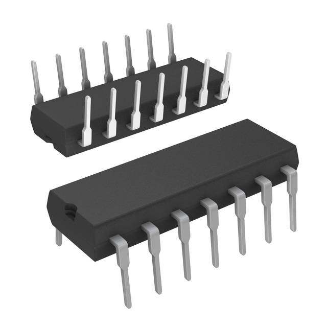
| 描述 | IC SWITCH QUAD SP4T 16TVSOP模拟开关 IC 14-Ohm Dual SP4T Analog Switch |
| 产品分类 | |
| 品牌 | Texas Instruments |
| 产品手册 | |
| 产品图片 |
|
| rohs | 符合RoHS无铅 / 符合限制有害物质指令(RoHS)规范要求 |
| 产品系列 | 开关 IC,模拟开关 IC,Texas Instruments TS3A5017DGVR- |
| 数据手册 | |
| 产品型号 | TS3A5017DGVR |
| 产品培训模块 | http://www.digikey.cn/PTM/IndividualPTM.page?site=cn&lang=zhs&ptm=9646 |
| 产品种类 | 模拟开关 IC |
| 供应商器件封装 | 16-TVSOP |
| 其它名称 | 296-17582-6 |
| 制造商产品页 | http://www.ti.com/general/docs/suppproductinfo.tsp?distId=10&orderablePartNumber=TS3A5017DGVR |
| 功能 | |
| 包装 | Digi-Reel® |
| 单位重量 | 42 mg |
| 商标 | Texas Instruments |
| 安装类型 | 表面贴装 |
| 安装风格 | SMD/SMT |
| 导通电阻 | 12 欧姆 |
| 导通电阻—最大值 | 22 Ohms |
| 封装 | Reel |
| 封装/外壳 | 16-TFSOP (0.173",4.40mm 宽) |
| 封装/箱体 | TVSOP-16 |
| 工作温度 | -40°C ~ 85°C |
| 工作电源电压 | 2.3 V to 3.6 V |
| 工厂包装数量 | 2000 |
| 开关数量 | 2 |
| 开关配置 | SP4T |
| 最大工作温度 | + 85 C |
| 最小工作温度 | - 40 C |
| 标准包装 | 1 |
| 电压-电源,单/双 (±) | 2.3 V ~ 3.6 V |
| 电压源 | 单电源 |
| 电流-电源 | 2.5µA |
| 电源电压-最大 | 3.6 V |
| 电源电压-最小 | 2.3 V |
| 电源电流 | 2.5 uA |
| 电源电流—最大值 | 10 uA |
| 电路 | 2 x SP4T |
| 空闲时间—最大值 | 4.5 ns |
| 系列 | TS3A5017 |
| 运行时间—最大值 | 9.5 ns |


- 商务部:美国ITC正式对集成电路等产品启动337调查
- 曝三星4nm工艺存在良率问题 高通将骁龙8 Gen1或转产台积电
- 太阳诱电将投资9.5亿元在常州建新厂生产MLCC 预计2023年完工
- 英特尔发布欧洲新工厂建设计划 深化IDM 2.0 战略
- 台积电先进制程称霸业界 有大客户加持明年业绩稳了
- 达到5530亿美元!SIA预计今年全球半导体销售额将创下新高
- 英特尔拟将自动驾驶子公司Mobileye上市 估值或超500亿美元
- 三星加码芯片和SET,合并消费电子和移动部门,撤换高东真等 CEO
- 三星电子宣布重大人事变动 还合并消费电子和移动部门
- 海关总署:前11个月进口集成电路产品价值2.52万亿元 增长14.8%


PDF Datasheet 数据手册内容提取
Product Order Technical Tools & Support & Folder Now Documents Software Community TS3A5017 SCDS188G–JANUARY2005–REVISEDJANUARY2019 TS3A5017 Dual SP4T Analog Switch / Multiplexer / Demultiplexer 1 Features 3 Description • IsolationinthePowered-DownMode,V =0 The TS3A5017 device is a dual single-pole 1 + quadruple-throw (4:1) analog switch that is designed • LowON-StateResistance to operate from 2.3 V to 3.6 V. This device can • LowChargeInjection handle both digital and analog signals, and signals up • ExcellentON-StateResistanceMatching toV+canbetransmittedineitherdirection. • LowTotalHarmonicDistortion(THD) DeviceInformation(1) • 2.3-Vto3.6-VSingle-SupplyOperation PARTNUMBER PACKAGE BODYSIZE(NOM) • Latch-UpPerformanceExceeds100mAPer SOIC(16) 9.90mm×3.90mm JESD78,ClassII SSOP(16) 4.90mm×3.90mm • ESDPerformanceTestedPerJESD22 TSSOP(16) 5.00mm×4.40mm – 1500-VHuman-BodyModel TS3A5017 TVSOP(16) 4.40mm×3.60mm (A114-B,ClassII) UQFN(16) 2.50mm×1.80mm – 1000-VCharged-DeviceModel(C101) VQFN(16) 4.00mm×3.50mm 2 Applications (1) For all available packages, see the orderable addendum at theendofthedatasheet. • Sample-and-HoldCircuits • Battery-PoweredEquipment • AudioandVideoSignalRouting • CommunicationCircuits BlockDiagram EN IN1 IN2 D S1 S2 S3 S4 1 An IMPORTANT NOTICE at the end of this data sheet addresses availability, warranty, changes, use in safety-critical applications, intellectualpropertymattersandotherimportantdisclaimers.PRODUCTIONDATA.
TS3A5017 SCDS188G–JANUARY2005–REVISEDJANUARY2019 www.ti.com Table of Contents 1 Features.................................................................. 1 8.2 FunctionalBlockDiagram.......................................14 2 Applications........................................................... 1 8.3 FeatureDescription.................................................14 3 Description............................................................. 1 8.4 DeviceFunctionalModes........................................15 4 RevisionHistory..................................................... 2 9 ApplicationandImplementation........................ 16 9.1 ApplicationInformation............................................16 5 PinConfigurationandFunctions......................... 3 9.2 TypicalApplication .................................................16 6 Specifications......................................................... 4 10 PowerSupplyRecommendations..................... 17 6.1 AbsoluteMaximumRatings......................................4 11 Layout................................................................... 17 6.2 ESDRatings ............................................................4 6.3 RecommendedOperatingConditions.......................4 11.1 LayoutGuidelines.................................................17 6.4 ThermalInformation..................................................4 11.2 LayoutExample....................................................18 6.5 ElectricalCharacteristicsfor3.3-VSupply................5 12 DeviceandDocumentationSupport................. 19 6.6 ElectricalCharacteristicsfor2.5-VSupply................6 12.1 DeviceSupport......................................................19 6.7 SwitchingCharacteristicsfor3.3-Vsupply................7 12.2 DocumentationSupport........................................20 6.8 SwitchingCharacteristicsfor2.5-Vsupply................7 12.3 Trademarks...........................................................20 6.9 TypicalCharacteristics..............................................8 12.4 ElectrostaticDischargeCaution............................20 7 ParameterMeasurementInformation................10 12.5 Glossary................................................................20 8 DetailedDescription............................................ 14 13 Mechanical,Packaging,andOrderable Information........................................................... 21 8.1 Overview.................................................................14 4 Revision History ChangesfromRevisionF(October2018)toRevisionG Page • ChangedFeatureFrom:2000-VHuman-BodyModelTo:1500-VHuman-BodyModel ....................................................... 1 • ChangedtheHBMvalueFrom:±2000VTo:±1500VintheESDRatings........................................................................... 4 ChangesfromRevisionE(April2015)toRevisionF Page • ChangedtheX MAXvalueFrom:–49dBTo–69dBintheElectricalCharacteristicsfor3.3-VSupply......................... 6 TALK ChangesfromRevisionD(December2008)toRevisionE Page • AddedApplications,DeviceInformationtable,PinFunctionstable,ESDRatingstable,ThermalInformationtable, TypicalCharacteristics,FeatureDescriptionsection,DeviceFunctionalModes,ApplicationandImplementation section,PowerSupplyRecommendationssection,Layoutsection,DeviceandDocumentationSupportsection,and Mechanical,Packaging,andOrderableInformationsection.................................................................................................. 1 • DeletedOrderingInformationtable........................................................................................................................................ 1 2 SubmitDocumentationFeedback Copyright©2005–2019,TexasInstrumentsIncorporated ProductFolderLinks:TS3A5017
TS3A5017 www.ti.com SCDS188G–JANUARY2005–REVISEDJANUARY2019 5 Pin Configuration and Functions D,DBQ,DGV,andPWPackage 16-PinSOIC,SSOP,TVSOPandTSSOP RGYPackage (TopView) 16-PinVQFN (TopView) 1EN 1 CLoongtricol CLoongtricol 16 V+ 1EN V+ IN2 2 15 2EN 1 16 1S4 3 14 IN1 IN2 2 15 2EN 1S3 4 13 2S4 1S4 3 14 IN1 1S2 5 12 2S3 1S3 4 ECxpenotseerd 13 2S4 1S1 6 11 2S2 1S2 5 Pad 12 2S3 1D 7 10 2S1 11SD1 76 1101 22SS21 GND 8 9 2D 8 9 GND 2D Ifexposedcenterpadisused,itmustbe connectedasasecondarygroundorleft electricallyopen. RSVPackage 16-PinUQFN (TopView) N2 EN + EN I 1V 2 16 15 14 13 1S4 1 12 IN1 1S3 2 11 2S4 1S2 3 10 2S3 1S1 4 9 2S2 5 6 7 8 D D D 1 1 N 2 2S G PinFunctions PIN SOIC,SSOP,TVSOP, TYPE DESCRIPTION NAME UQFNNO. TSSOP,VQFNNO. 1D 7 5 I/O Commonpathforswitch1 1EN 1 15 I Active-lowenableforswitch1 1S1 6 4 I/O Switch1channel1 1S2 5 3 I/O Switch1channel2 1S3 4 2 I/O Switch1channel3 1S4 3 1 I/O Switch1channel4 2D 9 7 I/O Commonpathforswitch2 2EN 15 13 I Active-lowenableforswitch2 2S1 10 8 I/O Switch2channel1 2S2 11 9 I/O Switch2channel2 2S3 12 10 I/O Switch2channel3 2S4 13 11 I/O Switch2channel4 GND 8 6 – Ground IN1 14 12 I Switch1inputselect IN2 2 16 I Switch2inputselect V+ 16 14 – Supplyvoltage Copyright©2005–2019,TexasInstrumentsIncorporated SubmitDocumentationFeedback 3 ProductFolderLinks:TS3A5017
TS3A5017 SCDS188G–JANUARY2005–REVISEDJANUARY2019 www.ti.com 6 Specifications 6.1 Absolute Maximum Ratings overoperatingfree-airtemperaturerange(unlessotherwisenoted)(1)(2) MIN MAX UNIT V Supplyvoltage(3) –0.5 4.6 V + V ,V Analogvoltage(3)(4) –0.5 4.6 V S D I , SK Analogportclampcurrent V ,V <0 –50 mA I S D DK I ,I ON-stateswitchcurrent V ,V =0to7V –128 128 mA S D S D V Digitalinputvoltage –0.5 4.6 V I I Digitalinputclampcurrent(3)(4) V <0 –50 mA IK I I ContinuouscurrentthroughV 100 mA + + I ContinuouscurrentthroughGND –100 mA GND T Storagetemperature –65 150 °C stg (1) StressesbeyondthoselistedunderAbsoluteMaximumRatingsmaycausepermanentdamagetothedevice.Thesearestressratings only,andfunctionaloperationofthedeviceattheseoranyotherconditionsbeyondthoseindicatedunderRecommendedOperating Conditionsisnotimplied.Exposuretoabsolute-maximum-ratedconditionsforextendedperiodsmayaffectdevicereliability. (2) Thealgebraicconvention,wherebythemostnegativevalueisaminimumandthemostpositivevalueisamaximum. (3) Allvoltagesarewithrespecttoground,unlessotherwisespecified. (4) Theinputandoutputvoltageratingsmaybeexceedediftheinputandoutputclamp-currentratingsareobserved. 6.2 ESD Ratings VALUE UNIT Human-bodymodel(HBM),perANSI/ESDA/JEDECJS-001(1) ±1500 V(ESD) Electrostaticdischarge Charged-devicemodel(CDM),perJEDECspecificationJESD22- ±1000 V C101(2) (1) JEDECdocumentJEP155statesthat500-VHBMallowssafemanufacturingwithastandardESDcontrolprocess. (2) JEDECdocumentJEP157statesthat250-VCDMallowssafemanufacturingwithastandardESDcontrolprocess. 6.3 Recommended Operating Conditions overoperatingfree-airtemperaturerange(unlessotherwisenoted) MIN MAX UNIT V Switchinput/outputvoltagerange 0 3.6 V I/O V+ Supplyvoltagerange 2.3 3.6 V V Controlinputvoltagerange 0 3.6 V I T OperatingTemperatureRange –40 85 °C A 6.4 Thermal Information TS3A5018 THERMALMETRIC(1) D(SOIC) DBQ DGV PW RGY RSV(UQFN) UNIT (SSOP) (TVSOP) (TSSOP) (VQFN) 16PINS 16PINS 16PINS 16PINS 16PINS 16PINS R Junction-to-ambientthermalresistance 73 82 120 108 91.6 184 °C/W θJA (1) Formoreinformationabouttraditionalandnewthermalmetrics,seetheICPackageThermalMetricsapplicationreport,SPRA953. 4 SubmitDocumentationFeedback Copyright©2005–2019,TexasInstrumentsIncorporated ProductFolderLinks:TS3A5017
TS3A5017 www.ti.com SCDS188G–JANUARY2005–REVISEDJANUARY2019 6.5 Electrical Characteristics for 3.3-V Supply V =2.7Vto3.6V,T =–40°Cto85°C(unlessotherwisenoted)(1) + A PARAMETER TESTCONDITIONS T V MIN TYP MAX UNIT A + AnalogSwitch Analogsignal V ,V 0 V V D S range + ON-state 0≤V ≤V , SwitchON, 25°C 11 12 r S + 3V Ω on resistance ID=–32mA, seeFigure12 Full 14 ON-state 25°C 1 2 resistance V =2.1V, SwitchON, Δr match S 3V Ω on between ID=–32mA, seeFigure12 Full 3 channels ON-state 25°C 7 9 0≤V ≤V , SwitchON, r resistance S + 3V Ω on(flat) flatness ID=–32mA, seeFigure12 Full 10 V =1V,V =3V, 25°C –0.1 0.05 0.1 S D I or 3.6V S(OFF) S V =3V,V =1V, SwitchOFF, Full –0.2 0.2 OFFleakage S D μA seeFigure13 current V =0to3.6V, 25°C –1 0.5 1 I S 0V SPWR(OFF) VD=3.6Vto0, Full –5 5 V =1V,V =3V, 25°C –0.1 0.05 0.1 S D I or 3.6V D(OFF) D V =3V,V =1V, SwitchOFF, Full –0.2 0.2 OFFleakage S D μA seeFigure13 current V =0to3.6V, 25°C –1 0.5 1 I D 0V DPWR(OFF) VS=3.6Vto0, Full –5 5 S V =1V,V =Open, 25°C –0.1 0.05 0.1 S D SwitchON, I ONleakage or 3.6V μA S(ON) current V =3V,V =Open, seeFigure14 Full –0.2 0.2 S D D V =1V,V =Open, 25°C –0.1 0.05 0.1 D S SwitchON, I ONleakage or 3.6V μA D(ON) current V =3V,V =Open, seeFigure14 Full –0.2 0.2 D S DigitalControlInputs(IN1,IN2,EN)(2) V Inputlogichigh Full 2 V V IH + V Inputlogiclow Full 0 0.8 V IL Inputleakage 25°C –1 0.05 1 I ,I V =V or0 3.6V μA IH IL current I + Full –1 1 V =0,R =0, Q Chargeinjection GEN GEN SeeFigure21 25°C 3.3V 5 pC C C =0.1nF, L S V =V orGND, C OFF S + SeeFigure15 25°C 3.3V 4.5 pF S(OFF) SwitchOFF, capacitance D V =V orGND, C OFF D + SeeFigure15 25°C 3.3V 19 pF D(OFF) SwitchOFF, capacitance S V =V orGND, C S + SeeFigure15 25°C 3.3V 25 pF S(ON) ONcapacitance SwitchON, D V =V orGND, C D + SeeFigure15 25°C 3.3V 25 pF D(ON) ONcapacitance SwitchON, Digitalinput C V =V orGND, SeeFigure15 25°C 3.3V 2 pF I capacitance I + R =50Ω, BW Bandwidth L SeeFigure17 25°C 3.3V 165 MHz SwitchON, R =50Ω, O OFFisolation L SeeFigure18 25°C 3.3V –69 dB ISO f=1MHz, (1) Thealgebraicconvention,wherebythemostnegativevalueisaminimumandthemostpositivevalueisamaximum (2) AllunuseddigitalinputsofthedevicemustbeheldatV orGNDtoensureproperdeviceoperation.RefertotheTIapplicationreport, + ImplicationsofSloworFloatingCMOSInputs,literaturenumberSCBA004. Copyright©2005–2019,TexasInstrumentsIncorporated SubmitDocumentationFeedback 5 ProductFolderLinks:TS3A5017
TS3A5017 SCDS188G–JANUARY2005–REVISEDJANUARY2019 www.ti.com Electrical Characteristics for 3.3-V Supply (continued) V =2.7Vto3.6V,T =–40°Cto85°C(unlessotherwisenoted)(1) + A PARAMETER TESTCONDITIONS T V MIN TYP MAX UNIT A + R =50Ω, X Crosstalk L SeeFigure19 25°C 3.3V –-69 dB TALK f=1MHz, Crosstalk R =50Ω, X L SeeFigure20 25°C 3.3V –74 dB TALK(ADJ) adjacent f=1MHz, Totalharmonic R =600Ω, f=20Hzto20kHz, THD L 25°C 3.3V 0.21% distortion C =50pF, seeFigure22 L Supply Positivesupply 25°C 2.5 7 I V =V orGND, SwitchONorOFF 3.6V μA + current I + Full 10 6.6 Electrical Characteristics for 2.5-V Supply V =2.3Vto2.7V,T =–40°Cto85°C(unlessotherwisenoted)(1) + A PARAMETER TESTCONDITIONS T V MIN TYP MAX UNIT A + AnalogSwitch Analogsignal V ,V 0 V V D S range + ON-state 0≤V ≤V , SwitchON, 25°C 20.5 22 r S + 2.3V Ω on resistance ID=–24mA, seeFigure12 Full 24 ON-state 25°C 1 2 V =1.6V, SwitchON, Δr resistancematch S 2.3V Ω on betweenchannels ID=–24mA, seeFigure12 Full 3 ON-state 0≤V ≤V , SwitchON, 25°C 16 18 r S + 2.3V Ω on(flat) resistanceflatness ID=–24mA, seeFigure12 Full 20 V =0.5V,V =2.2V, 25°C –0.1 0.05 0.1 S D I or 2.7V S(OFF) S V =2.2V,V =0.5V, SwitchOFF, Full –0.2 0.2 OFFleakage S D μA seeFigure13 current V =0to2.7V, 25°C –1 0.5 1 I S 0V SPWR(OFF) VD=2.7Vto0, Full –5 5 V =0.5V,V =2.2V, 25°C –0.1 0.05 0.1 S D I or 2.7V D(OFF) D V =2.2V,V =0.5V, SwitchOFF, Full –0.2 0.2 OFFleakage S D μA seeFigure13 current V =0to2.7V, 25°C –1 0.5 1 I D 0V DPWR(OFF) VS=2.7Vto0, Full –5 5 S V =0.5V,V =Open, 25°C –0.1 0.05 0.1 S D SwitchON, I ONleakage or 2.7V μA S(ON) current V =2.2V,V =Open, seeFigure14 Full –0.2 0.2 S D D V =0.5V,V =Open, 25°C –0.1 0.05 0.1 D S SwitchON, I ONleakage or 2.7V μA D(ON) current V =2.2V,V =Open, seeFigure14 Full –0.2 0.2 D S DigitalControlInputs(IN1,IN2,EN)(2) V Inputlogichigh Full 1.7 V V IH + V Inputlogiclow Full 0 0.7 V IL Inputleakage 25°C –1 0.05 1 I ,I V =V or0 2.7V μA IH IL current I + Full –1 1 V =0,R =0, Q Chargeinjection GEN GEN SeeFigure21 25°C 2.5V pC C C =0.1nF, L S V =V orGND, C S + SeeFigure15 25°C 2.5V 4.5 pF S(OFF) OFFcapacitance SwitchOFF, (1) Thealgebraicconvention,wherebythemostnegativevalueisaminimumandthemostpositivevalueisamaximum (2) AllunuseddigitalinputsofthedevicemustbeheldatV orGNDtoensureproperdeviceoperation.RefertotheTIapplicationreport, + ImplicationsofSloworFloatingCMOSInputs,literaturenumberSCBA004. 6 SubmitDocumentationFeedback Copyright©2005–2019,TexasInstrumentsIncorporated ProductFolderLinks:TS3A5017
TS3A5017 www.ti.com SCDS188G–JANUARY2005–REVISEDJANUARY2019 Electrical Characteristics for 2.5-V Supply (continued) V =2.3Vto2.7V,T =–40°Cto85°C(unlessotherwisenoted)(1) + A PARAMETER TESTCONDITIONS T V MIN TYP MAX UNIT A + D V =V orGND, C D + SeeFigure15 25°C 2.5V 18.5 pF D(OFF) OFFcapacitance SwitchOFF, S V =V orGND, C S + SeeFigure15 25°C 2.5V 24 pF S(ON) ONcapacitance SwitchON, D V =V orGND, C D + SeeFigure15 25°C 2.5V 24 pF D(ON) ONcapacitance SwitchON, Digitalinput C V =V orGND, SeeFigure15 25°C 2.5V 2 pF I capacitance I + R =50Ω, BW Bandwidth L SeeFigure17 25°C 2.5V 165 MHz SwitchON, R =50Ω, O OFFisolation L SeeFigure18 25°C 2.5V –69 dB ISO f=1MHz, R =50Ω, X Crosstalk L SeeFigure19 25°C 2.5V –69 dB TALK f=1MHz, R =50Ω, X Crosstalkadjacent L SeeFigure20 25°C 2.5V –74 dB TALK(ADJ) f=1MHz, Totalharmonic R =600Ω, f=20Hzto20kHz, THD L 25°C 2.5V 0.29% distortion C =50pF, seeFigure22 L Supply Positivesupply 25°C 2.5 7 I V =V orGND, SwitchONorOFF 2.7V μA + current I + Full 10 6.7 Switching Characteristics for 3.3-V supply overoperatingfree-airtemperaturerange(unlessotherwisenoted) PARAMETER TESTCONDITIONS T V MIN TYP MAX UNIT A + 25°C 3.3V 1 5 9.5 V =2V, C =35pF, tON Turnontime RDL=300Ω, seLeFigure16 Full 3Vto 1 10.5 ns 3.6V 25°C 3.3V 0.5 1.5 3.5 V =2V, C =35pF, tOFF Turnofftime RDL=300Ω, seLeFigure16 Full 3Vto 0.5 4.5 ns 3.6V 6.8 Switching Characteristics for 2.5-V supply overoperatingfree-airtemperaturerange(unlessotherwisenoted) PARAMETER TESTCONDITIONS T V MIN TYP MAX UNIT A + 25°C 2.5V 1.5 5 8 V =2V, C =35pF, tON Turnontime RCLO=M300Ω, seLeFigure16 Full 2.3Vto 1 10 ns 2.7V 25°C 2.5V 0.3 2 4.5 V =2V, C =35pF, tOFF Turnofftime RCLO=M300Ω, seLeFigure16 Full 2.3Vto 0.3 6 ns 2.7V Copyright©2005–2019,TexasInstrumentsIncorporated SubmitDocumentationFeedback 7 ProductFolderLinks:TS3A5017
TS3A5017 SCDS188G–JANUARY2005–REVISEDJANUARY2019 www.ti.com 6.9 Typical Characteristics 18 12 T = 25°C 16 A 10 14 V = 2.5V + 85°C 12 8 25°C Ω) 10 Ω) (ON 8 (ON 6 r r 6 V = 3.3V 4 + 4 –40°C 2 2 0 0 0 1 2 3 4 0.0 0.5 1.0 1.5 2.0 2.5 3.0 3.5 V (V) V (V) COM COM Figure1.r vsV Figure2.r vsV (V =3.3V) on COM on COM + 18 40 I 16 NC(ON) I 14 COM(ON) 30 A) I 12 n NO(ON) Ω) 10 85°C nt ( r(ON 68 25°C e Curre 20 INC(OFF) ICOM(OFF) g a 4 ak 10 e 2 –40°C L INO(OFF) 0 0 0.0 0.5 1.0 1.5 2.0 2.5 3.0 –40 25 85 VCOM(V) TA(°C) Figure3.ronvsVCOM(V+=2.5V) Figure4.LeakageCurrentvsTemperature(V+=3.6V) 4.5 9 4.0 V = 3.3V 8 t + ON 3.5 7 C) 3.0 6 p ge Injection ( 212...055 V+= 2.5V /t(ns)ONOFF 435 tOFF ar 1.0 t 2 h C 1 0.5 0 0.0 2.0 2.5 3.0 3.5 4.0 0.0 0.5 1.0 1.5 2.0 2.5 3.0 3.5 VCOM(V) V+(V) Figure5.ChargeInjection(QC)vsVCOM Figure6.tONandtOFFvsSupplyVoltage 8 SubmitDocumentationFeedback Copyright©2005–2019,TexasInstrumentsIncorporated ProductFolderLinks:TS3A5017
TS3A5017 www.ti.com SCDS188G–JANUARY2005–REVISEDJANUARY2019 Typical Characteristics (continued) 2.0 1.8 A) 1.6 n d ( 1.4 VIH ol sh 1.2 VIL e hr 1.0 T el 0.8 v e L 0.6 c- gi 0.4 o L 0.2 0.0 2.0 2.2 2.4 2.6 2.8 3.0 3.2 3.4 3.6 3.8 4.0 V (V) + Figure7.Logic-LevelThresholdvsV+ Figure8.Bandwidth(GainvsFrequency)(V+=3.3V) 0.35 0.30 0.25 %) D ( H 0.20 T 0.15 0.10 10 100 1000 10 K 100 K Frequency(Hz) Figure9.OFFIsolationandCrosstalkvsFrequency Figure10.TotalHarmonicDistortionvsFrequency (V =3.3V) + A) µ ( (°C) Figure11.Power-SupplyCurrentvsTemperature (V =3.6V) + Copyright©2005–2019,TexasInstrumentsIncorporated SubmitDocumentationFeedback 9 ProductFolderLinks:TS3A5017
TS3A5017 SCDS188G–JANUARY2005–REVISEDJANUARY2019 www.ti.com 7 Parameter Measurement Information Channel ON V –V or V ron= D S2-IS4 s1 Ω D V = V or V I IH IL Figure12. ON-StateResistance(r ) on OFF-State Leakage Current Channel OFF V = V or V I IH IL V or V = 0 to V S1 S2-S4 + and V = V to 0 D + Figure13. OFF-StateLeakageCurrent(I ,I ) D(OFF) S(OFF) ON-State Leakage Current Channel ON V = V or V I IH IL Figure14. ON-StateLeakageCurrent(I ,I ) D(ON) S(ON) 10 SubmitDocumentationFeedback Copyright©2005–2019,TexasInstrumentsIncorporated ProductFolderLinks:TS3A5017
TS3A5017 www.ti.com SCDS188G–JANUARY2005–REVISEDJANUARY2019 Parameter Measurement Information (continued) V = V to GND BIAS + V = V or V I IH IL Capacitance is measured at S1, S2-S4, D, and IN inputs during ON and OFF conditions. Figure15. Capacitance(C,C ,C ,C ,C ) I D(OFF) D(ON) S(OFF) S(ON) C L 300Ω 35 pF (C) (B) 300Ω 35 pF V + (B) 0 (A) t OFF A. All input pulses are supplied by generators having the following characteristics: PRR≤10MHz,Z =50Ω,t <5ns,t <5ns. O r f B. C includesprobeandjigcapacitance. L C. SeeElectricalCharacteristicsforV . D Figure16. Turnon(t )andTurnoffTime(t ) ON OFF Channel ON: S to D 1 50Ω V = V or GND I + NetworkAnalyzer Setup Source Power = 0 dBm 50Ω (632-mV P-Pat 50-Ωload) DC Bias = 350 mV Figure17. Bandwidth(BW) Copyright©2005–2019,TexasInstrumentsIncorporated SubmitDocumentationFeedback 11 ProductFolderLinks:TS3A5017
TS3A5017 SCDS188G–JANUARY2005–REVISEDJANUARY2019 www.ti.com Parameter Measurement Information (continued) Channel OFF: S to D 50Ω V = V or GND I + 50Ω NetworkAnalyzer Setup Source Power = 0 dBm 50Ω (632-mV P-Pat 50-Ωload) DC Bias = 350 mV Figure18. OFFIsolation(O ) ISO Channel ON: S to D 1 Channel OFF: S -S to D 2 4 50Ω V = V or GND I + V S2-S4 NetworkAnalyzer Setup Source Power = 0 dBm 50Ω 50Ω (632-mV P-Pat 50-Ωload) DC Bias = 350 mV Figure19. Crosstalk(X ) TALK 50Ω V1S 1S1 Channel ON: S1to D 1D V 2S 2S 1 50Ω NetworkAnalyzer Setup 2D Source Power = 0 dBm 50Ω (632-mV P-Pat 50-Ωload) DC Bias = 350 mV Figure20. AdjacentCrosstalk(X ) TALK 12 SubmitDocumentationFeedback Copyright©2005–2019,TexasInstrumentsIncorporated ProductFolderLinks:TS3A5017
TS3A5017 www.ti.com SCDS188G–JANUARY2005–REVISEDJANUARY2019 Parameter Measurement Information (continued) V IH V IL ΔV D V = 0 to V GEN + R = 0 GEN C = 0.1 nF L QC= CLXΔVD V = V or V I IH IL A. All input pulses are supplied by generators having the following characteristics: PRR≤10MHz,Z =50Ω,t <5ns,t <5ns. O r f B. C includesprobeandjigcapacitance. L Figure21. ChargeInjection(Q ) C 10 µF 10 µF (A) 600Ω 600Ω 600Ω A. C includesprobeandjigcapacitance. L Figure22. TotalHarmonicDistortion(THD) Copyright©2005–2019,TexasInstrumentsIncorporated SubmitDocumentationFeedback 13 ProductFolderLinks:TS3A5017
TS3A5017 SCDS188G–JANUARY2005–REVISEDJANUARY2019 www.ti.com 8 Detailed Description 8.1 Overview The TS3A5017 is a dual Single-Pole-4-Throw (SP4T) solid-state analog switch. The TS3A5017, like all analog switches,isbidirectional.EachDpinconnectstoitsfourrespectiveSpins,withtheswitchconnectiondependent onthestatusofEN,IN2,andIN1.SeeTable1fortheswitchconfigurationtruthtable. 8.2 Functional Block Diagram EN IN1 IN2 D S1 S2 S3 S4 Figure23. FunctionalBlockDiagram(EachSwitch) 8.3 Feature Description Isolationinpowered-downmodeallowssignalstobepresentattheinputswhiletheswitchispoweredoffwithout causing damage to the device. The low ON-state resistance and low charge injection give the TS3A5017 better performanceathigherspeeds. 14 SubmitDocumentationFeedback Copyright©2005–2019,TexasInstrumentsIncorporated ProductFolderLinks:TS3A5017
TS3A5017 www.ti.com SCDS188G–JANUARY2005–REVISEDJANUARY2019 8.4 Device Functional Modes Table1.FunctionTable DTOS, EN IN2 IN1 STOD L L L D=S1 L L H D=S2 L H L D=S3 L H H D=S4 H X X OFF Copyright©2005–2019,TexasInstrumentsIncorporated SubmitDocumentationFeedback 15 ProductFolderLinks:TS3A5017
TS3A5017 SCDS188G–JANUARY2005–REVISEDJANUARY2019 www.ti.com 9 Application and Implementation NOTE Information in the following applications sections is not part of the TI component specification, and TI does not warrant its accuracy or completeness. TI’s customers are responsible for determining suitability of components for their purposes. Customers should validateandtesttheirdesignimplementationtoconfirmsystemfunctionality. 9.1 Application Information The TS3A5018 can be used in a variety of customer systems. The TS3A5018 can be used anywhere multiple analogordigitalsignalsmustbeselectedtopassacrossasingleline. 9.2 Typical Application 3.3 V V+ EN S1 IN1 S2 To/From System (cid:29)C or System IN2 S3 Logic D S4 GND Figure24. SystemSchematicforTS3A5017 9.2.1 DesignRequirements In this particular application, V+ was 3.3 V, although V+ is allowed to be any voltage specified in Recommended Operating Conditions. A decoupling capacitor is recommended on the V+ pin. See Power Supply Recommendationsformoredetails. 9.2.2 DetailedDesignProcedure In this application, EN, IN1, and IN2 are, by default, pulled low to GND. Choose these resistor sizes based on the current driving strength of the GPIO, the desired power consumption, and the switching frequency (if applicable).IftheGPIOisopen-drain,usepullupresistorsinstead. 16 SubmitDocumentationFeedback Copyright©2005–2019,TexasInstrumentsIncorporated ProductFolderLinks:TS3A5017
TS3A5017 www.ti.com SCDS188G–JANUARY2005–REVISEDJANUARY2019 Typical Application (continued) 9.2.3 ApplicationCurve 5.0 4.5 4.0 t ON 3.5 ns) 3.0 ( FF 2.5 O /tN 2.0 tOFF O t 1.5 1.0 0.5 0.0 –40 25 85 T (°C) A Figure25. t andt vsTemperature(V =3.3V) ON OFF + 10 Power Supply Recommendations The power supply can be any voltage between the minimum and maximum supply voltage rating located in the RecommendedOperatingConditions. Each V terminal should have a good bypass capacitor to prevent power disturbance. For devices with a single CC supply, a 0.1-μF bypass capacitor is recommended. If there are multiple pins labeled V , then a 0.01-μF or CC 0.022-μF capacitor is recommended for each V because the V pins will be tied together internally. For CC CC devices with dual-supply pins operating at different voltages, for example V and V , a 0.1-µF bypass CC DD capacitor is recommended for each supply pin. It is acceptable to parallel multiple bypass capacitors to reject different frequencies of noise. 0.1-μF and 1-μF capacitors are commonly used in parallel. The bypass capacitor shouldbeinstalledasclosetothepowerterminalaspossibleforbestresults. 11 Layout 11.1 Layout Guidelines Reflections and matching are closely related to loop antenna theory, but different enough to warrant their own discussion. When a PCB trace turns a corner at a 90° angle, a reflection can occur. This is primarily due to the change of width of the trace. At the apex of the turn, the trace width is increased to 1.414 times its width. This upsets the transmission line characteristics, especially the distributed capacitance and self–inductance of the trace — resulting in the reflection. It is a given that not all PCB traces can be straight, and so they will have to turn corners. Below figure shows progressively better techniques of rounding corners. Only the last example maintainsconstanttracewidthandminimizesreflections. Unused switch I/Os, such as NO, NC, and COM, can be left floating or tied to GND. However, the IN1, IN2, and EN pins must be driven high or low. Due to partial transistor turnon when control inputs are at threshold levels, floating control inputs can cause increased I or unknown switch selection states. See Implications of Slow or CC FloatingCMOSInputs,SCBA004formoredetails. Copyright©2005–2019,TexasInstrumentsIncorporated SubmitDocumentationFeedback 17 ProductFolderLinks:TS3A5017
TS3A5017 SCDS188G–JANUARY2005–REVISEDJANUARY2019 www.ti.com 11.2 Layout Example WORST BETTER BEST W 2 1W min. W Figure26. TraceExample 18 SubmitDocumentationFeedback Copyright©2005–2019,TexasInstrumentsIncorporated ProductFolderLinks:TS3A5017
TS3A5017 www.ti.com SCDS188G–JANUARY2005–REVISEDJANUARY2019 12 Device and Documentation Support 12.1 Device Support 12.1.1 DeviceNomenclature Table2.ParameterDescription SYMBOL DESCRIPTION V VoltageatCOM COM V VoltageatNC NC V VoltageatNO NO r ResistancebetweenCOMandNCorNOportswhenthechannelisON on Δr Differenceofr betweenchannelsinaspecificdevice on on r Differencebetweenthemaximumandminimumvalueofr inachanneloverthespecifiedrangeofconditions on(flat) on I LeakagecurrentmeasuredattheNCport,withthecorrespondingchannel(NCtoCOM)intheOFFstate NC(OFF) LeakagecurrentmeasuredattheNCport,withthecorrespondingchannel(NCtoCOM)intheONstateandtheoutput I NC(ON) (COM)open I LeakagecurrentmeasuredattheNOport,withthecorrespondingchannel(NOtoCOM)intheOFFstate NO(OFF) LeakagecurrentmeasuredattheNOport,withthecorrespondingchannel(NOtoCOM)intheONstateandtheoutput I NO(ON) (COM)open I LeakagecurrentmeasuredattheCOMport,withthecorrespondingchannel(COMtoNCorNO)intheOFFstate COM(OFF) LeakagecurrentmeasuredattheCOMport,withthecorrespondingchannel(COMtoNCorNO)intheONstateandthe I COM(ON) output(NCorNO)open V Minimuminputvoltageforlogichighforthecontrolinput(IN,EN) IH V Maximuminputvoltageforlogiclowforthecontrolinput(IN,EN) IL V Voltageatthecontrolinput(IN,EN) I I ,I Leakagecurrentmeasuredatthecontrolinput(IN,EN) IH IL Turnontimefortheswitch.Thisparameterismeasuredunderthespecifiedrangeofconditionsandbythepropagation t ON delaybetweenthedigitalcontrol(IN)signalandanalogoutputNCorNO)signalwhentheswitchisturningON. Turnofftimefortheswitch.Thisparameterismeasuredunderthespecifiedrangeofconditionsandbythepropagation t OFF delaybetweenthedigitalcontrol(IN)signalandanalogoutput(NCorNO)signalwhentheswitchisturningOFF. Chargeinjectionisameasurementofunwantedsignalcouplingfromthecontrol(IN)inputtotheanalog(NCorNO) Q output.Thisismeasuredincoulomb(C)andmeasuredbythetotalchargeinducedduetoswitchingofthecontrolinput. C Chargeinjection,Q =C ×ΔV ,C istheloadcapacitanceandΔV isthechangeinanalogoutputvoltage. C L COM L COM C CapacitanceattheNCportwhenthecorrespondingchannel(NCtoCOM)isOFF NC(OFF) C CapacitanceattheNCportwhenthecorrespondingchannel(NCtoCOM)isON NC(ON) C CapacitanceattheNCportwhenthecorrespondingchannel(NOtoCOM)isOFF NO(OFF) C CapacitanceattheNCportwhenthecorrespondingchannel(NOtoCOM)isON NO(ON) C CapacitanceattheCOMportwhenthecorrespondingchannel(COMtoNC)isOFF COM(OFF) C CapacitanceattheCOMportwhenthecorrespondingchannel(COMtoNC)isON COM(ON) C Capacitanceofcontrolinput(IN,EN) I OFFisolationoftheswitchisameasurementofOFF-stateswitchimpedance.ThisismeasuredindBinaspecific O ISO frequency,withthecorrespondingchannel(NCtoCOM)intheOFFstate. CrosstalkisameasurementofunwantedsignalcouplingfromanONchanneltoanOFFchannel(NC1toNO1).Adjacent X crosstalkisameasureofunwantedsignalcouplingfromanONchanneltoanadjacentONchannel(NC1toNC2).Thisis TALK measuredinaspecificfrequencyandindB. BW Bandwidthoftheswitch.ThisisthefrequencyinwhichthegainofanONchannelis–3dBbelowtheDCgain. Totalharmonicdistortiondescribesthesignaldistortioncausedbytheanalogswitch.Thisisdefinedastheratioofroot THD meansquare(RMS)valueofthesecond,third,andhigherharmonictotheabsolutemagnitudeofthefundamental harmonic. I Staticpower-supplycurrentwiththecontrol(IN)pinatV orGND + + Copyright©2005–2019,TexasInstrumentsIncorporated SubmitDocumentationFeedback 19 ProductFolderLinks:TS3A5017
TS3A5017 SCDS188G–JANUARY2005–REVISEDJANUARY2019 www.ti.com 12.2 Documentation Support 12.2.1 RelatedDocumentation • ImplicationsofSloworFloatingCMOSInputs,SCBA004 12.3 Trademarks Alltrademarksarethepropertyoftheirrespectiveowners. 12.4 Electrostatic Discharge Caution Thesedeviceshavelimitedbuilt-inESDprotection.Theleadsshouldbeshortedtogetherorthedeviceplacedinconductivefoam duringstorageorhandlingtopreventelectrostaticdamagetotheMOSgates. 12.5 Glossary SLYZ022—TIGlossary. Thisglossarylistsandexplainsterms,acronyms,anddefinitions. 20 SubmitDocumentationFeedback Copyright©2005–2019,TexasInstrumentsIncorporated ProductFolderLinks:TS3A5017
TS3A5017 www.ti.com SCDS188G–JANUARY2005–REVISEDJANUARY2019 13 Mechanical, Packaging, and Orderable Information The following pages include mechanical, packaging, and orderable information. This information is the most current data available for the designated devices. This data is subject to change without notice and revision of thisdocument.Forbrowser-basedversionsofthisdatasheet,refertotheleft-handnavigation. Copyright©2005–2019,TexasInstrumentsIncorporated SubmitDocumentationFeedback 21 ProductFolderLinks:TS3A5017
PACKAGE OPTION ADDENDUM www.ti.com 6-Feb-2020 PACKAGING INFORMATION Orderable Device Status Package Type Package Pins Package Eco Plan Lead/Ball Finish MSL Peak Temp Op Temp (°C) Device Marking Samples (1) Drawing Qty (2) (6) (3) (4/5) TS3A5017D ACTIVE SOIC D 16 40 Green (RoHS NIPDAU Level-1-260C-UNLIM -40 to 85 TS3A5017 & no Sb/Br) TS3A5017DBQR ACTIVE SSOP DBQ 16 2500 Green (RoHS NIPDAU Level-2-260C-1 YEAR -40 to 85 YA017 & no Sb/Br) TS3A5017DGVR ACTIVE TVSOP DGV 16 2000 Green (RoHS NIPDAU Level-1-260C-UNLIM -40 to 85 YA017 & no Sb/Br) TS3A5017DR ACTIVE SOIC D 16 2500 Green (RoHS NIPDAU Level-1-260C-UNLIM -40 to 85 TS3A5017 & no Sb/Br) TS3A5017PW ACTIVE TSSOP PW 16 90 Green (RoHS NIPDAU Level-1-260C-UNLIM -40 to 85 YA017 & no Sb/Br) TS3A5017PWG4 ACTIVE TSSOP PW 16 90 Green (RoHS NIPDAU Level-1-260C-UNLIM -40 to 85 YA017 & no Sb/Br) TS3A5017PWR ACTIVE TSSOP PW 16 2000 Green (RoHS NIPDAU Level-1-260C-UNLIM -40 to 85 YA017 & no Sb/Br) TS3A5017PWRG4 ACTIVE TSSOP PW 16 2000 Green (RoHS NIPDAU Level-1-260C-UNLIM -40 to 85 YA017 & no Sb/Br) TS3A5017RGYR ACTIVE VQFN RGY 16 3000 Green (RoHS NIPDAU Level-2-260C-1 YEAR -40 to 85 YA017 & no Sb/Br) TS3A5017RGYRG4 ACTIVE VQFN RGY 16 3000 Green (RoHS NIPDAU Level-2-260C-1 YEAR -40 to 85 YA017 & no Sb/Br) TS3A5017RSVR ACTIVE UQFN RSV 16 3000 Green (RoHS NIPDAU Level-1-260C-UNLIM -40 to 85 ZVL & no Sb/Br) (1) The marketing status values are defined as follows: ACTIVE: Product device recommended for new designs. LIFEBUY: TI has announced that the device will be discontinued, and a lifetime-buy period is in effect. NRND: Not recommended for new designs. Device is in production to support existing customers, but TI does not recommend using this part in a new design. PREVIEW: Device has been announced but is not in production. Samples may or may not be available. OBSOLETE: TI has discontinued the production of the device. (2) RoHS: TI defines "RoHS" to mean semiconductor products that are compliant with the current EU RoHS requirements for all 10 RoHS substances, including the requirement that RoHS substance do not exceed 0.1% by weight in homogeneous materials. Where designed to be soldered at high temperatures, "RoHS" products are suitable for use in specified lead-free processes. TI may reference these types of products as "Pb-Free". RoHS Exempt: TI defines "RoHS Exempt" to mean products that contain lead but are compliant with EU RoHS pursuant to a specific EU RoHS exemption. Green: TI defines "Green" to mean the content of Chlorine (Cl) and Bromine (Br) based flame retardants meet JS709B low halogen requirements of <=1000ppm threshold. Antimony trioxide based flame retardants must also meet the <=1000ppm threshold requirement. Addendum-Page 1
PACKAGE OPTION ADDENDUM www.ti.com 6-Feb-2020 (3) MSL, Peak Temp. - The Moisture Sensitivity Level rating according to the JEDEC industry standard classifications, and peak solder temperature. (4) There may be additional marking, which relates to the logo, the lot trace code information, or the environmental category on the device. (5) Multiple Device Markings will be inside parentheses. Only one Device Marking contained in parentheses and separated by a "~" will appear on a device. If a line is indented then it is a continuation of the previous line and the two combined represent the entire Device Marking for that device. (6) Lead/Ball Finish - Orderable Devices may have multiple material finish options. Finish options are separated by a vertical ruled line. Lead/Ball Finish values may wrap to two lines if the finish value exceeds the maximum column width. Important Information and Disclaimer:The information provided on this page represents TI's knowledge and belief as of the date that it is provided. TI bases its knowledge and belief on information provided by third parties, and makes no representation or warranty as to the accuracy of such information. Efforts are underway to better integrate information from third parties. TI has taken and continues to take reasonable steps to provide representative and accurate information but may not have conducted destructive testing or chemical analysis on incoming materials and chemicals. TI and TI suppliers consider certain information to be proprietary, and thus CAS numbers and other limited information may not be available for release. In no event shall TI's liability arising out of such information exceed the total purchase price of the TI part(s) at issue in this document sold by TI to Customer on an annual basis. OTHER QUALIFIED VERSIONS OF TS3A5017 : •Automotive: TS3A5017-Q1 NOTE: Qualified Version Definitions: •Automotive - Q100 devices qualified for high-reliability automotive applications targeting zero defects Addendum-Page 2
PACKAGE MATERIALS INFORMATION www.ti.com 17-Dec-2018 TAPE AND REEL INFORMATION *Alldimensionsarenominal Device Package Package Pins SPQ Reel Reel A0 B0 K0 P1 W Pin1 Type Drawing Diameter Width (mm) (mm) (mm) (mm) (mm) Quadrant (mm) W1(mm) TS3A5017DBQR SSOP DBQ 16 2500 330.0 12.5 6.4 5.2 2.1 8.0 12.0 Q1 TS3A5017DGVR TVSOP DGV 16 2000 330.0 12.4 6.8 4.0 1.6 8.0 12.0 Q1 TS3A5017DR SOIC D 16 2500 330.0 16.4 6.5 10.3 2.1 8.0 16.0 Q1 TS3A5017PWR TSSOP PW 16 2000 330.0 12.4 6.9 5.6 1.6 8.0 12.0 Q1 TS3A5017RGYR VQFN RGY 16 3000 330.0 12.4 3.8 4.3 1.5 8.0 12.0 Q1 TS3A5017RSVR UQFN RSV 16 3000 180.0 12.4 2.1 2.9 0.75 4.0 12.0 Q1 PackMaterials-Page1
PACKAGE MATERIALS INFORMATION www.ti.com 17-Dec-2018 *Alldimensionsarenominal Device PackageType PackageDrawing Pins SPQ Length(mm) Width(mm) Height(mm) TS3A5017DBQR SSOP DBQ 16 2500 340.5 338.1 20.6 TS3A5017DGVR TVSOP DGV 16 2000 367.0 367.0 35.0 TS3A5017DR SOIC D 16 2500 333.2 345.9 28.6 TS3A5017PWR TSSOP PW 16 2000 367.0 367.0 35.0 TS3A5017RGYR VQFN RGY 16 3000 367.0 367.0 35.0 TS3A5017RSVR UQFN RSV 16 3000 203.0 203.0 35.0 PackMaterials-Page2
MECHANICAL DATA MPDS006C – FEBRUARY 1996 – REVISED AUGUST 2000 DGV (R-PDSO-G**) PLASTIC SMALL-OUTLINE 24 PINS SHOWN 0,23 0,40 0,07 M 0,13 24 13 0,16 NOM 4,50 6,60 4,30 6,20 Gage Plane 0,25 0°–(cid:1)8° 0,75 1 12 0,50 A Seating Plane 0,15 1,20 MAX 0,08 0,05 PINS ** 14 16 20 24 38 48 56 DIM A MAX 3,70 3,70 5,10 5,10 7,90 9,80 11,40 A MIN 3,50 3,50 4,90 4,90 7,70 9,60 11,20 4073251/E 08/00 NOTES: A. All linear dimensions are in millimeters. B. This drawing is subject to change without notice. C. Body dimensions do not include mold flash or protrusion, not to exceed 0,15 per side. D. Falls within JEDEC: 24/48 Pins – MO-153 14/16/20/56 Pins – MO-194 • POST OFFICE BOX 655303 DALLAS, TEXAS 75265
None
PACKAGE OUTLINE DBQ0016A SSOP - 1.75 mm max height SCALE 2.800 SHRINK SMALL-OUTLINE PACKAGE C SEATING PLANE .228-.244 TYP [5.80-6.19] .004 [0.1] C A PIN 1 ID AREA 14X .0250 [0.635] 16 1 2X .189-.197 .175 [4.81-5.00] [4.45] NOTE 3 8 9 16X .008-.012 B .150-.157 [0.21-0.30] .069 MAX [3.81-3.98] [1.75] NOTE 4 .007 [0.17] C A B .005-.010 TYP [0.13-0.25] SEE DETAIL A .010 [0.25] GAGE PLANE .004-.010 0 - 8 [0.11-0.25] .016-.035 [0.41-0.88] DETAIL A (.041 ) TYPICAL [1.04] 4214846/A 03/2014 NOTES: 1. Linear dimensions are in inches [millimeters]. Dimensions in parenthesis are for reference only. Controlling dimensions are in inches. Dimensioning and tolerancing per ASME Y14.5M. 2. This drawing is subject to change without notice. 3. This dimension does not include mold flash, protrusions, or gate burrs. Mold flash, protrusions, or gate burrs shall not exceed .006 inch, per side. 4. This dimension does not include interlead flash. 5. Reference JEDEC registration MO-137, variation AB. www.ti.com
EXAMPLE BOARD LAYOUT DBQ0016A SSOP - 1.75 mm max height SHRINK SMALL-OUTLINE PACKAGE 16X (.063) [1.6] SYMM SEE DETAILS 1 16 16X (.016 ) [0.41] 14X (.0250 ) [0.635] 8 9 (.213) [5.4] LAND PATTERN EXAMPLE SCALE:8X SOLDER MASK SOLDER MASK METAL OPENING OPENING METAL .002 MAX .002 MIN [0.05] [0.05] ALL AROUND ALL AROUND NON SOLDER MASK SOLDER MASK DEFINED DEFINED SOLDER MASK DETAILS 4214846/A 03/2014 NOTES: (continued) 6. Publication IPC-7351 may have alternate designs. 7. Solder mask tolerances between and around signal pads can vary based on board fabrication site. www.ti.com
EXAMPLE STENCIL DESIGN DBQ0016A SSOP - 1.75 mm max height SHRINK SMALL-OUTLINE PACKAGE 16X (.063) [1.6] SYMM 1 16 16X (.016 ) [0.41] SYMM 14X (.0250 ) [0.635] 8 9 (.213) [5.4] SOLDER PASTE EXAMPLE BASED ON .005 INCH [0.127 MM] THICK STENCIL SCALE:8X 4214846/A 03/2014 NOTES: (continued) 8. Laser cutting apertures with trapezoidal walls and rounded corners may offer better paste release. IPC-7525 may have alternate design recommendations. 9. Board assembly site may have different recommendations for stencil design. www.ti.com
None
None
None
PACKAGE OUTLINE RSV0016A UQFN - 0.55 mm max height SCALE 5.000 ULTRA THIN QUAD FLATPACK - NO LEAD 1.85 B A 1.75 PIN 1 INDEX AREA 2.65 2.55 0.55 C 0.45 SEATING PLANE 0.05 0.05 C 0.00 2X 1.2 SYMM (0.13) TYP 5 ℄ 8 0.45 15X 0.35 4 9 SYMM 2X 1.2 ℄ 12X 0.4 1 0.25 12 16X 0.15 0.07 C A B 0.05 16 13 0.55 0.45 PIN 1 ID (45 X 0.1) ° 4220314/C 02/2020 NOTES: 1. All linear dimensions are in millimeters. Any dimensions in parenthesis are for reference only. Dimensioning and tolerancing per ASME Y14.5M. 2. This drawing is subject to change without notice. www.ti.com
EXAMPLE BOARD LAYOUT RSV0016A UQFN - 0.55 mm max height ULTRA THIN QUAD FLATPACK - NO LEAD SYMM (0.7) ℄ 16 13 SEE SOLDER MASK DETAIL 16X (0.2) 1 12 SYMM 12X (0.4) (2.4) ℄ (R0.05) TYP 4 9 15X (0.6) 5 8 (1.6) LAND PATTERN EXAMPLE EXPOSED METAL SHOWN SCALE: 25X 0.05 MIN 0.05 MAX ALL AROUND ALL AROUND METAL UNDER METAL EDGE SOLDER MASK EXPOSED METAL SOLDER MASK EXPOSED SOLDER MASK OPENING METAL OPENING NON SOLDER MASK DEFINED SOLDER MASK DEFINED (PREFERRED) SOLDER MASK DETAILS 4220314/C 02/2020 NOTES: (continued) 3. For more information, see Texas Instruments literature number SLUA271 (www.ti.com/lit/slua271). www.ti.com
EXAMPLE STENCIL DESIGN RSV0016A UQFN - 0.55 mm max height ULTRA THIN QUAD FLATPACK - NO LEAD (0.7) 16 13 16X (0.2) 1 12 SYMM 12X (0.4) (2.4) ℄ (R0.05) TYP 4 9 15X (0.6) 5 8 SYMM ℄ (1.6) SOLDER PASTE EXAMPLE BASED ON 0.125 MM THICK STENCIL SCALE: 25X 4220314/C 02/2020 NOTES: (continued) 4. Laser cutting apertures with trapezoidal walls and rounded corners may offer better paste release. IPC-7525 may have alternate design recommendations. www.ti.com
None
None
PACKAGE OUTLINE PW0016A TSSOP - 1.2 mm max height SCALE 2.500 SMALL OUTLINE PACKAGE SEATING PLANE C 6.6 TYP 6.2 A 0.1 C PIN 1 INDEX AREA 14X 0.65 16 1 2X 5.1 4.55 4.9 NOTE 3 8 9 0.30 B 4.5 16X 0.19 1.2 MAX 4.3 0.1 C A B NOTE 4 (0.15) TYP SEE DETAIL A 0.25 GAGE PLANE 0.15 0.05 0.75 0.50 0 -8 DETA 20AIL A TYPICAL 4220204/A 02/2017 NOTES: 1. All linear dimensions are in millimeters. Any dimensions in parenthesis are for reference only. Dimensioning and tolerancing per ASME Y14.5M. 2. This drawing is subject to change without notice. 3. This dimension does not include mold flash, protrusions, or gate burrs. Mold flash, protrusions, or gate burrs shall not exceed 0.15 mm per side. 4. This dimension does not include interlead flash. Interlead flash shall not exceed 0.25 mm per side. 5. Reference JEDEC registration MO-153. www.ti.com
EXAMPLE BOARD LAYOUT PW0016A TSSOP - 1.2 mm max height SMALL OUTLINE PACKAGE 16X (1.5) SYMM (R0.05) TYP 1 16X (0.45) 16 SYMM 14X (0.65) 8 9 (5.8) LAND PATTERN EXAMPLE EXPOSED METAL SHOWN SCALE: 10X SOLDER MASK METAL UNDER SOLDER MASK OPENING METAL SOLDER MASK OPENING EXPOSED METAL EXPOSED METAL 0.05 MAX 0.05 MIN ALL AROUND ALL AROUND NON-SOLDER MASK SOLDER MASK DEFINED DEFINED (PREFERRED) SOLDE15.000R MASK DETAILS 4220204/A 02/2017 NOTES: (continued) 6. Publication IPC-7351 may have alternate designs. 7. Solder mask tolerances between and around signal pads can vary based on board fabrication site. www.ti.com
EXAMPLE STENCIL DESIGN PW0016A TSSOP - 1.2 mm max height SMALL OUTLINE PACKAGE 16X (1.5) SYMM (R0.05) TYP 1 16X (0.45) 16 SYMM 14X (0.65) 8 9 (5.8) SOLDER PASTE EXAMPLE BASED ON 0.125 mm THICK STENCIL SCALE: 10X 4220204/A 02/2017 NOTES: (continued) 8. Laser cutting apertures with trapezoidal walls and rounded corners may offer better paste release. IPC-7525 may have alternate design recommendations. 9. Board assembly site may have different recommendations for stencil design. www.ti.com
IMPORTANTNOTICEANDDISCLAIMER TI PROVIDES TECHNICAL AND RELIABILITY DATA (INCLUDING DATASHEETS), DESIGN RESOURCES (INCLUDING REFERENCE DESIGNS), APPLICATION OR OTHER DESIGN ADVICE, WEB TOOLS, SAFETY INFORMATION, AND OTHER RESOURCES “AS IS” AND WITH ALL FAULTS, AND DISCLAIMS ALL WARRANTIES, EXPRESS AND IMPLIED, INCLUDING WITHOUT LIMITATION ANY IMPLIED WARRANTIES OF MERCHANTABILITY, FITNESS FOR A PARTICULAR PURPOSE OR NON-INFRINGEMENT OF THIRD PARTY INTELLECTUAL PROPERTY RIGHTS. These resources are intended for skilled developers designing with TI products. You are solely responsible for (1) selecting the appropriate TI products for your application, (2) designing, validating and testing your application, and (3) ensuring your application meets applicable standards, and any other safety, security, or other requirements. These resources are subject to change without notice. TI grants you permission to use these resources only for development of an application that uses the TI products described in the resource. Other reproduction and display of these resources is prohibited. No license is granted to any other TI intellectual property right or to any third party intellectual property right. TI disclaims responsibility for, and you will fully indemnify TI and its representatives against, any claims, damages, costs, losses, and liabilities arising out of your use of these resources. TI’s products are provided subject to TI’s Terms of Sale (www.ti.com/legal/termsofsale.html) or other applicable terms available either on ti.com or provided in conjunction with such TI products. TI’s provision of these resources does not expand or otherwise alter TI’s applicable warranties or warranty disclaimers for TI products. Mailing Address: Texas Instruments, Post Office Box 655303, Dallas, Texas 75265 Copyright © 2020, Texas Instruments Incorporated