ICGOO在线商城 > 集成电路(IC) > 接口 - 驱动器,接收器,收发器 > TRS3237EIDBR
 Datasheet下载
- 型号: TRS3237EIDBR
- 制造商: Texas Instruments
- 库位|库存: xxxx|xxxx
- 要求:
| 数量阶梯 | 香港交货 | 国内含税 |
| +xxxx | $xxxx | ¥xxxx |
查看当月历史价格
查看今年历史价格
TRS3237EIDBR产品简介:
ICGOO电子元器件商城为您提供TRS3237EIDBR由Texas Instruments设计生产,在icgoo商城现货销售,并且可以通过原厂、代理商等渠道进行代购。 TRS3237EIDBR价格参考。Texas InstrumentsTRS3237EIDBR封装/规格:接口 - 驱动器,接收器,收发器, 全 收发器 5/3 RS232 28-SSOP。您可以下载TRS3237EIDBR参考资料、Datasheet数据手册功能说明书,资料中有TRS3237EIDBR 详细功能的应用电路图电压和使用方法及教程。
Texas Instruments 的 TRS3237EIDBR 是一款 RS-232 接口芯片,属于接口类中的驱动器/接收器/收发器。它主要用于实现数字信号在不同设备之间的串行通信,尤其是在工业控制、通信设备和嵌入式系统中应用广泛。

该芯片支持 5V 电源供电,具备高数据传输速率(最高可达 250 kbps),具有较强的抗干扰能力,适合在工业环境下使用。其主要功能是将 TTL/CMOS 电平转换为 RS-232 电平,实现微控制器或计算机与其他外围设备之间的可靠通信。

典型应用场景包括:

1. 工业自动化系统:用于PLC(可编程逻辑控制器)、传感器、执行器之间的串口通信。
2. 通信设备:如调制解调器、路由器、交换机等设备中作为串口通信接口。
3. 嵌入式系统开发板:用于连接PC与嵌入式系统的串口调试接口。
4. 仪器仪表:用于测试设备、测量仪器与上位机之间的数据传输。
5. 控制系统:如楼宇自动化、安防系统中实现设备间的远程通信。

总之,TRS3237EIDBR 在需要稳定、远距离串口通信的场合中具有广泛应用。
| 参数 | 数值 |
| 产品目录 | 集成电路 (IC) |
| 描述 | IC MULTICH RS232 DVR/RCVR 28SSOP |
| 产品分类 | |
| 品牌 | Texas Instruments |
| 数据手册 | |
| 产品图片 |
|
| 产品型号 | TRS3237EIDBR |
| rohs | 无铅 / 符合限制有害物质指令(RoHS)规范要求 |
| 产品系列 | - |
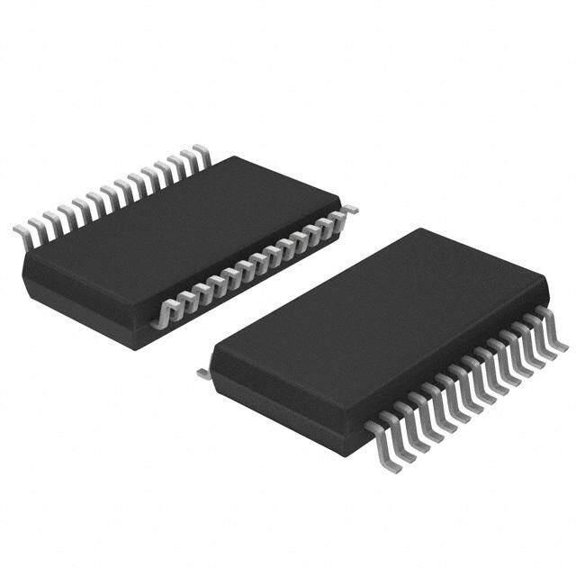
| 供应商器件封装 | 28-SSOP |
| 其它名称 | 296-22599-6 |
| 包装 | Digi-Reel® |
| 协议 | RS232 |
| 双工 | 全 |
| 安装类型 | 表面贴装 |
| 封装/外壳 | 28-SSOP(0.209",5.30mm 宽) |
| 工作温度 | -40°C ~ 85°C |
| 接收器滞后 | 500mV |
| 数据速率 | 1Mbps |
| 标准包装 | 1 |
| 电压-电源 | 3 V ~ 5.5 V |
| 类型 | 收发器 |
| 驱动器/接收器数 | 5/3 |


PDF Datasheet 数据手册内容提取
TRS3237E www.ti.com SLLS796A–JUNE2007–REVISEDJANUARY2010 3-V TO 5.5-V MULTICHANNEL RS-232 1-MBit/s LINE DRIVER/RECEIVER CheckforSamples:TRS3237E FEATURES 1 • MeetsorExceedstheRequirementsof • ESDProtectionforRS-232I/OPins TIA/EIA-232-FandITUv.28Standards – ±15kV –Human-BodyModel(HBM) • OperatesWith3-Vto5.5-VVCCSupply – ±8kV – IEC61000-4-2,ContactDischarge • OperatesFrom250kbits/sto1Mbit/s – ±15kV –IEC61000-4-2,Air-GapDischarge • LowStandbyCurrent...1mATypical APPLICATIONS • ExternalCapacitors...4×0.1mF • Battery-Powered,Hand-Held,andPortable • Accepts5-VLogicInputWith3.3-VSupply Equipment • DesignedtoBeInterchangeableWithIndustry • PDAsandPalmtopPCs Standard'3237EDevices • Notebooks,Sub-Notebooks,andLaptops • Latch-UpPerformanceExceeds100mAPer • DigitalCameras JESD78,ClassII • MobilePhonesandWirelessDevices DB, DW, OR PW PACKAGE RHB PACKAGE (TOP VIEW) (TOP VIEW) GCN2D+ 12 2287 CV+1+ V−C2–GNDC2+C1+V+VCCN.C. C2− 3 26 VCC 3231 30 29282726 25 V− 4 25 C1− DOUT1 1 24 C1– DOUT1 5 24 DIN1 DOUT2 2 23 DIN1 DOUT2 6 23 DIN2 DOUT3 3 22 IN2 DOUT3 7 22 DIN3 RIN1 4 21 DIN3 RIN1 8 21 ROUT1 RIN2 5 20 ROUT1 RIN2 9 20 ROUT2 DOUT4 6 19 ROUT2 DOUT4 10 19 DIN4 RIN3 7 18 DIN4 RIN3 11 18 ROUT3 N.C. 8 17 ROUT3 DOUT5 12 17 DIN5 9 10111213 141516 EN 13 16 ROUT1B SHDN 14 15 MBAUD OUT5ENSHDNBAUDN.C.UT1BDIN5N.C. D M O R N.C.– Not internally connected DESCRIPTION/ORDERING INFORMATION TheTRS3237Econsistsoffivelinedrivers,threelinereceivers,andadualcharge-pumpcircuitwith±15-kVESD protection pin to pin (serial-port connection pins, including GND). The device meets the requirements of TIA/EIA-232-F and provides the electrical interface between an asynchronous communication controller and the serial-port connector. The charge pump and four small external capacitors allow operation from a single 3-V to 5.5-V supply. This device operates at data signaling rates of 250 kbit/s in normal operating mode (MBAUD=GND)and1Mbit/swhenMBAUD=V .Thedriveroutputslewrateisamaximumof30V/ms. CC 1 Pleasebeawarethatanimportantnoticeconcerningavailability,standardwarranty,anduseincriticalapplicationsofTexas Instrumentssemiconductorproductsanddisclaimerstheretoappearsattheendofthisdatasheet. PRODUCTIONDATAinformationiscurrentasofpublicationdate. Copyright©2007–2010,TexasInstrumentsIncorporated Products conform to specifications per the terms of the Texas Instruments standard warranty. Production processing does not necessarilyincludetestingofallparameters.
TRS3237E SLLS796A–JUNE2007–REVISEDJANUARY2010 www.ti.com The TRS3237E transmitters are disabled and the outputs are forced into high-impedance state when the device is in shutdown mode (SHDN = GND) and the supply current falls to less than 1 mA. Also, during shutdown, the onboard charge pump is disabled; V+ is lowered to V , and V– is raised toward GND. Receiver outputs also CC can be placed in the high-impedance state by setting enable (EN) high. ROUT1B remains active all the time, regardlessoftheENandSHDNcondition. The TRS3237EC is characterized for operation from 0°C to 70°C. The TRS3237EI is characterized for operation from–40°Cto85°C. Table1. ORDERINGINFORMATION(1) T PACKAGE(2) ORDERABLEPARTNUMBER TOP-SIDEMARKING A SSOP–DB Reelof2000 TRS3237ECDBR TRS3237EC SOIC–DW Reelof2000 TRS3237ECDWR TRS3237EC 0°Cto70°C TSSOP–PW Reelof2000 TRS3237ECPWR RS37EC QFN–RHB Reelof2000 TRS3237ECRHBR PREVIEW SSOP–DB Reelof2000 TRS3237EIDBR TRS3237EI SOIC–DW Reelof2000 TRS3237EIDWR TRS3237EI –40°Cto85°C TSSOP–PW Reelof2000 TRS3237EIPWR RS37EI QFN–RHB Reelof2000 TRS3237EIRHBR PREVIEW (1) Forthemostcurrentpackageandorderinginformation,seethePackageOptionAddendumattheendofthisdocument,orseetheTI websiteatwww.ti.com. (2) Packagedrawings,thermaldata,andsymbolizationareavailableatwww.ti.com/packaging. Table2.FUNCTIONTABLE INPUTS OUTPUTS SHDN EN DOUT ROUT ROUT1B 0 0 Z(1) Active Active 0 1 Z(1) Z(1) Active 1 0 Active Active Active 1 1 Active Z(1) Active (1) Z=highimpedance(off) 2 SubmitDocumentationFeedback Copyright©2007–2010,TexasInstrumentsIncorporated ProductFolderLink(s):TRS3237E
TRS3237E www.ti.com SLLS796A–JUNE2007–REVISEDJANUARY2010 LOGICDIAGRAM(POSITIVELOGIC) 24 5 DIN1 DOUT1 23 6 DIN2 DOUT2 22 7 DIN3 DOUT3 19 10 DIN4 DOUT4 17 12 DIN5 DOUT5 14 SHDN 15 MBAUD 16 ROUT1B 21 8 ROUT1 RIN1 20 9 ROUT2 RIN2 18 11 ROUT3 RIN3 13 EN Copyright©2007–2010,TexasInstrumentsIncorporated SubmitDocumentationFeedback 3 ProductFolderLink(s):TRS3237E
TRS3237E SLLS796A–JUNE2007–REVISEDJANUARY2010 www.ti.com ABSOLUTE MAXIMUM RATINGS(1) overoperatingfree-airtemperaturerange(unlessotherwisenoted) MIN MAX UNIT V Supplyvoltagerange(2) –0.3 6 V CC V+ Positive-outputsupplyvoltagerange(2) –0.3 7 V V– Negative-outputsupplyvoltagerange(2) 0.3 –7 V V+–V– Supplyvoltagedifference(2) 13 V Driver(SHDN,MBAUD,EN) –0.3 6 V Inputvoltagerange V I Receiver –25 25 Driver –13.2 13.2 V Outputvoltagerange V O Receiver –0.3 V +0.3 CC Short-circuitduration DOUTtoGND Unlimited q Packagethermalimpedance(3) 62 °C/W JA T Storagetemperaturerange –65 150 °C stg (1) Stressesbeyondthoselistedunder"absolutemaximumratings"maycausepermanentdamagetothedevice.Thesearestressratings only,andfunctionaloperationofthedeviceattheseoranyotherconditionsbeyondthoseindicatedunder"recommendedoperating conditions"isnotimplied.Exposuretoabsolute-maximum-ratedconditionsforextendedperiodsmayaffectdevicereliability. (2) AllvoltagesarewithrespecttonetworkGND. (3) ThepackagethermalimpedanceiscalculatedinaccordancewithJESD51-7. RECOMMENDED OPERATING CONDITIONS(1) SeeFigure5 MIN NOM MAX UNIT V =3.3V 3 3.3 3.6 CC Supplyvoltage V V =5V 4.5 5 5.5 CC V =3.3V 2 5.5 CC V Driverandcontrolhigh-levelinputvoltage DIN,SHDN,MBAUD,EN V IH V =5V 2.4 5.5 CC V Driverandcontrollow-levelinputvoltage DIN,SHDN,MBAUD,EN 0 0.8 V IL V Receiverinputvoltage –25 25 V I TRS3237EC 0 70 T Operatingfree-airtemperature °C A TRS3237EI –40 85 (1) TestconditionsareC1–C4=0.1mFatV =3Vto5V. CC ELECTRICAL CHARACTERISTICS(1) overrecommendedrangesofsupplyvoltageandoperatingfree-airtemperature(unlessotherwisenoted)(seeFigure5) PARAMETER TESTCONDITIONS MIN TYP(2) MAX UNIT I Inputleakagecurrent DIN,SHDN,MBAUD,EN 9 18 mA I Noload,SHDN=V 0.5 2 mA CC Supplycurrent SHDN=GND 1 10 mA I CC (TA=25°C) Shutdownsupplycurrent SHDN=RIN=GND, 10 300 nA DIN=GNDorV CC (1) TestconditionsareC1–C4=0.1mFatV =3Vto5V. CC (2) AlltypicalvaluesareatV =3.3VorV =5V,andT =25°C. CC CC A 4 SubmitDocumentationFeedback Copyright©2007–2010,TexasInstrumentsIncorporated ProductFolderLink(s):TRS3237E
TRS3237E www.ti.com SLLS796A–JUNE2007–REVISEDJANUARY2010 DRIVER SECTION ELECTRICAL CHARACTERISTICS(1) overrecommendedrangesofsupplyvoltageandoperatingfree-airtemperature(unlessotherwisenoted)(seeFigure5) PARAMETER TESTCONDITIONS MIN TYP(2) MAX UNIT V High-leveloutputvoltage DOUTatR =3kΩtoGND, DIN=GND 5 5.4 V OH L V Low-leveloutputvoltage DOUTatR =3kΩtoGND, DIN=V –5 –5.4 V OL L CC I High-levelinputcurrent V =V ±0.01 ±1 mA IH I CC I Low-levelinputcurrent V atGND ±0.01 ±1 mA IL I I Short-circuitoutputcurrent(3) V =3.6Vor3.3V, V =0V ±60 mA OS CC O r Outputresistance V ,V ,andV =0V, V =±2V 300 50k Ω o CC + – O (1) TestconditionsareC1–C4=0.1mFatV =3Vto5V. CC (2) AlltypicalvaluesareatV =3.3VorV =5V,andT =25°C. CC CC A (3) Short-circuitdurationsshouldbecontrolledtopreventexceedingthedeviceabsolutepower-dissipationratings,andnotmorethanone outputshouldbeshortedatatime. DRIVER SECTION SWITCHING CHARACTERISTICS(1) overrecommendedrangesofsupplyvoltageandoperatingfree-airtemperature(unlessotherwisenoted)(seeFigure5) PARAMETER TESTCONDITIONS MIN TYP(2) MAX UNIT C =1000pF, L 250 MBAUD=GND C =1000pF, L V =4.5Vto5.5V, R =3kΩ,1DINswitching, 1000 Maximumdatarate CC L kbit/s MBAUD=V SeeFigure1 CC C =250pF, L V =3Vto4.5V, 1000 CC MBAUD=V CC t Pulseskew(3) CL=150pFto2500pF,RL=3kΩto7kΩ, 100 ns sk(p) MBAUD=V orGND,SeeFigure2 CC MBAUD= 6 30 Slewrate, VCC=3.3V, CL=150pFto1000pF GND SR(tr) transitionregion R =3kΩto7kΩ, MBAUD=V 24 150 V/ms L CC (seeFigure1) T =25°C A C =150pFto2500 MBAUD= L 4 30 pF, GND (1) TestconditionsareC1–C4=0.1mFatV =3Vto5V. CC (2) AlltypicalvaluesareatV =3.3VorV =5V,andT =25°C. CC CC A (3) Pulseskewisdefinedas|t –t |ofeachchannelofthesamedevice. PLH PHL Copyright©2007–2010,TexasInstrumentsIncorporated SubmitDocumentationFeedback 5 ProductFolderLink(s):TRS3237E
TRS3237E SLLS796A–JUNE2007–REVISEDJANUARY2010 www.ti.com RECEIVER SECTION ELECTRICAL CHARACTERISTICS(1) overrecommendedrangesofsupplyvoltageandoperatingfree-airtemperature(unlessotherwisenoted)(seeFigure5) PARAMETER TESTCONDITIONS MIN TYP(2) MAX UNIT V High-leveloutputvoltage I =–1mA V –0.6 V –0.1 V OH OH CC CC V Low-leveloutputvoltage I =1mA 0.4 V OL OL V =3.3V 1.5 2.4 CC V Positive-goinginputthresholdvoltage V IT+ V =5V 2 2.4 CC V =3.3V 0.6 1.1 CC V Negative-goinginputthresholdvoltage V IT– V =5V 0.8 1.5 CC V Inputhysteresis(V –V ) 0.5 V hys IT+ IT– I Outputleakagecurrent EN=V ±0.05 ±10 mA oz CC r Inputresistance V =±3Vto±25V 3 5 7 kΩ i I (1) TestconditionsareC1–C4=0.1mFatV =3Vto.5V. CC (2) AlltypicalvaluesareatV =3.3VorV =5V,andT =25°C. CC CC A RECEIVER SECTION SWITCHING CHARACTERISTICS(1) overrecommendedrangesofsupplyvoltageandoperatingfree-airtemperature(unlessotherwisenoted) PARAMETER TESTCONDITIONS TYP(2) UNIT t Propagationdelaytime,low-tohigh-leveloutput C =150pF,SeeFigure3 150 ns PLH L t Propagationdelaytime,high-tolow-leveloutput C =150pF,SeeFigure3 150 ns PHL L t Outputenabletime C =150pF,R =3kΩ,SeeFigure4 2.6 ms en L L t Outputdisabletime C =150pF,R =3kΩ,SeeFigure4 2.4 ms dis L L t Pulseskew(3) SeeFigure3 50 ns sk(p) (1) TestconditionsareC1–C4=0.1mFatV =3Vto5V. CC (2) AlltypicalvaluesareatV =3.3VorV =5V,andT =25°C. CC CC A (3) Pulseskewisdefinedas|t –t |ofeachchannelofthesamedevice. PLH PHL ESD PROTECTION PIN TESTCONDITIONS TYP UNIT IEC61000-4-2,ContactDischarge ±8 DOUT,RIN kV IEC61000-4-2,Air-GapDischarge ±15 6 SubmitDocumentationFeedback Copyright©2007–2010,TexasInstrumentsIncorporated ProductFolderLink(s):TRS3237E
TRS3237E www.ti.com SLLS796A–JUNE2007–REVISEDJANUARY2010 PARAMETER MEASUREMENT INFORMATION 3 V Input RS-232 0 V Output Generator (see Note B) 50 W CL tTHL tTLH RL (see Note A) 3 V 3 V 3 V VOH Output SHDN = VCC −3 V −3 V VOL SR(tr)(cid:1) 6V TEST CIRCUIT t ort VOLTAGE WAVEFORMS THL TLH NOTES: A. CL includes probe and jig capacitance. B. The pulse generator has the following characteristics: PRR = 250 kbit/s, ZO = 50 W , 50% duty cycle, tr ≤ 10 ns, tf ≤ 10 ns. Figure1. DriverSlewRate 3 V RS-232 Input 1.5 V 1.5 V Output 0 V Generator 50 W (see Note B) RL C(sLe e Note A) tPHL tPLH 3 V VOH SHDN = VCC Output 50% 50% VOL TEST CIRCUIT VOLTAGE WAVEFORMS NOTES: A. CL includes probe and jig capacitance. B. The pulse generator has the following characteristics: PRR = 250 kbit/s, ZO = 50 W , 50% duty cycle, tr ≤ 10 ns, tf ≤ 10 ns. Figure2. DriverPulseSkew 3 V or 0 V 3 V EN = GND Input 1.5 V 1.5 V −3 V Output Generator 50 W tPHL tPLH (see Note B) CL (see Note A) 3 V VOH EN = GND Output 50% 50% VOL TEST CIRCUIT VOLTAGE WAVEFORMS NOTES: A. CL includes probe and jig capacitance. B. The pulse generator has the following characteristics: ZO = 50 W , 50% duty cycle, tr ≤ 10 ns, tf ≤ 10 ns. Figure3. ReceiverPropagationDelayTimes Copyright©2007–2010,TexasInstrumentsIncorporated SubmitDocumentationFeedback 7 ProductFolderLink(s):TRS3237E
TRS3237E SLLS796A–JUNE2007–REVISEDJANUARY2010 www.ti.com PARAMETER MEASUREMENT INFORMATION (continued) 3 V Input 1.5 V 1.5 V VCC GND −3 V S1 3 V or 0 V tPHZ tPZH RL (S1 at GND) (S1 at GND) 3 V or 0 V Output VOH Output 50% CL 0.3 V (see Note A) EN tPLZ tPZL Generator (S1 at VCC) (S1 at VCC) 50 W (see Note B) 0.3 V Output 50% VOL TEST CIRCUIT VOLTAGE WAVEFORMS NOTES: A. CL includes probe and jig capacitance. B. The pulse generator has the following characteristics: ZO = 50 W , 50% duty cycle, tr ≤ 10 ns, tf ≤ 10 ns. C. tPLZ and tPHZ are the same as tdis. D. tPZL and tPZH are the same as ten. Figure4. ReceiverEnableandDisableTimes 8 SubmitDocumentationFeedback Copyright©2007–2010,TexasInstrumentsIncorporated ProductFolderLink(s):TRS3237E
TRS3237E www.ti.com SLLS796A–JUNE2007–REVISEDJANUARY2010 APPLICATION INFORMATION + CBYPASS = 0.1 m F − 28 1 C1+ C2+ 27 V+ + 2 + C2 − GND − C3† + C1 3 C2− VCC 26 − 4 V− 25 − C1− C4 + 5 24 DOUT1 DIN1 6 23 DOUT2 DIN2 7 22 DOUT3 DIN3 8 21 RIN1 ROUT1 RS-232 Port 5 kW 9 20 Logic I/Os RIN2 ROUT2 5 kW 10 19 DOUT4 DIN4 11 18 RIN3 ROUT3 5 kW 12 17 DOUT5 DIN5 16 ROUT1B 13 15 EN MBAUD 14 SHDN †C3 can be connected to VCC or GND. NOTES: A. Resistor values shown are nominal. VCC vs CAPACITOR VALUES B. Nonpolarized ceramic capacitors are acceptable. If polarized tantalum or electrolytic capacitors are used, they should be connected as shown. VCC C1 C2, C3, and C4 3.3 V ± 0.15 V 0.1 m F 0.1 m F 3.3 V ± 0.3 V 0.22 m F 0.22 m F 5 V ± 0.5 V 0.047 m F 0.33 m F 3 V to 5.5 V 0.22 m F 1 m F Figure5. TypicalOperatingCircuitandCapacitorValues Copyright©2007–2010,TexasInstrumentsIncorporated SubmitDocumentationFeedback 9 ProductFolderLink(s):TRS3237E
PACKAGE OPTION ADDENDUM www.ti.com 6-Feb-2020 PACKAGING INFORMATION Orderable Device Status Package Type Package Pins Package Eco Plan Lead/Ball Finish MSL Peak Temp Op Temp (°C) Device Marking Samples (1) Drawing Qty (2) (6) (3) (4/5) TRS3237ECDB ACTIVE SSOP DB 28 50 Green (RoHS NIPDAU Level-1-260C-UNLIM 0 to 70 TRS3237EC & no Sb/Br) TRS3237ECDBR ACTIVE SSOP DB 28 2000 Green (RoHS NIPDAU Level-1-260C-UNLIM 0 to 70 TRS3237EC & no Sb/Br) TRS3237ECDWR ACTIVE SOIC DW 28 1000 Green (RoHS NIPDAU Level-1-260C-UNLIM 0 to 70 TRS3237EC & no Sb/Br) TRS3237ECPWR ACTIVE TSSOP PW 28 2000 Green (RoHS NIPDAU Level-1-260C-UNLIM 0 to 70 RS37EC & no Sb/Br) TRS3237EIDB ACTIVE SSOP DB 28 50 Green (RoHS NIPDAU Level-1-260C-UNLIM -40 to 85 TRS3237EI & no Sb/Br) TRS3237EIDBR ACTIVE SSOP DB 28 2000 Green (RoHS NIPDAU Level-1-260C-UNLIM -40 to 85 TRS3237EI & no Sb/Br) TRS3237EIDWR ACTIVE SOIC DW 28 1000 Green (RoHS NIPDAU Level-1-260C-UNLIM -40 to 85 TRS3237EI & no Sb/Br) TRS3237EIPWR ACTIVE TSSOP PW 28 2000 Green (RoHS NIPDAU Level-1-260C-UNLIM -40 to 85 RS37EI & no Sb/Br) (1) The marketing status values are defined as follows: ACTIVE: Product device recommended for new designs. LIFEBUY: TI has announced that the device will be discontinued, and a lifetime-buy period is in effect. NRND: Not recommended for new designs. Device is in production to support existing customers, but TI does not recommend using this part in a new design. PREVIEW: Device has been announced but is not in production. Samples may or may not be available. OBSOLETE: TI has discontinued the production of the device. (2) RoHS: TI defines "RoHS" to mean semiconductor products that are compliant with the current EU RoHS requirements for all 10 RoHS substances, including the requirement that RoHS substance do not exceed 0.1% by weight in homogeneous materials. Where designed to be soldered at high temperatures, "RoHS" products are suitable for use in specified lead-free processes. TI may reference these types of products as "Pb-Free". RoHS Exempt: TI defines "RoHS Exempt" to mean products that contain lead but are compliant with EU RoHS pursuant to a specific EU RoHS exemption. Green: TI defines "Green" to mean the content of Chlorine (Cl) and Bromine (Br) based flame retardants meet JS709B low halogen requirements of <=1000ppm threshold. Antimony trioxide based flame retardants must also meet the <=1000ppm threshold requirement. (3) MSL, Peak Temp. - The Moisture Sensitivity Level rating according to the JEDEC industry standard classifications, and peak solder temperature. (4) There may be additional marking, which relates to the logo, the lot trace code information, or the environmental category on the device. Addendum-Page 1
PACKAGE OPTION ADDENDUM www.ti.com 6-Feb-2020 (5) Multiple Device Markings will be inside parentheses. Only one Device Marking contained in parentheses and separated by a "~" will appear on a device. If a line is indented then it is a continuation of the previous line and the two combined represent the entire Device Marking for that device. (6) Lead/Ball Finish - Orderable Devices may have multiple material finish options. Finish options are separated by a vertical ruled line. Lead/Ball Finish values may wrap to two lines if the finish value exceeds the maximum column width. Important Information and Disclaimer:The information provided on this page represents TI's knowledge and belief as of the date that it is provided. TI bases its knowledge and belief on information provided by third parties, and makes no representation or warranty as to the accuracy of such information. Efforts are underway to better integrate information from third parties. TI has taken and continues to take reasonable steps to provide representative and accurate information but may not have conducted destructive testing or chemical analysis on incoming materials and chemicals. TI and TI suppliers consider certain information to be proprietary, and thus CAS numbers and other limited information may not be available for release. In no event shall TI's liability arising out of such information exceed the total purchase price of the TI part(s) at issue in this document sold by TI to Customer on an annual basis. Addendum-Page 2
PACKAGE MATERIALS INFORMATION www.ti.com 12-Feb-2019 TAPE AND REEL INFORMATION *Alldimensionsarenominal Device Package Package Pins SPQ Reel Reel A0 B0 K0 P1 W Pin1 Type Drawing Diameter Width (mm) (mm) (mm) (mm) (mm) Quadrant (mm) W1(mm) TRS3237ECDBR SSOP DB 28 2000 330.0 16.4 8.2 10.5 2.5 12.0 16.0 Q1 TRS3237ECDWR SOIC DW 28 1000 330.0 32.4 11.35 18.67 3.1 16.0 32.0 Q1 TRS3237ECPWR TSSOP PW 28 2000 330.0 16.4 6.9 10.2 1.8 12.0 16.0 Q1 TRS3237EIDBR SSOP DB 28 2000 330.0 16.4 8.2 10.5 2.5 12.0 16.0 Q1 TRS3237EIDWR SOIC DW 28 1000 330.0 32.4 11.35 18.67 3.1 16.0 32.0 Q1 TRS3237EIPWR TSSOP PW 28 2000 330.0 16.4 6.9 10.2 1.8 12.0 16.0 Q1 PackMaterials-Page1
PACKAGE MATERIALS INFORMATION www.ti.com 12-Feb-2019 *Alldimensionsarenominal Device PackageType PackageDrawing Pins SPQ Length(mm) Width(mm) Height(mm) TRS3237ECDBR SSOP DB 28 2000 367.0 367.0 38.0 TRS3237ECDWR SOIC DW 28 1000 350.0 350.0 66.0 TRS3237ECPWR TSSOP PW 28 2000 367.0 367.0 38.0 TRS3237EIDBR SSOP DB 28 2000 367.0 367.0 38.0 TRS3237EIDWR SOIC DW 28 1000 350.0 350.0 66.0 TRS3237EIPWR TSSOP PW 28 2000 367.0 367.0 38.0 PackMaterials-Page2
None
None
None
PACKAGE OUTLINE DB0028A SSOP - 2 mm max height SCALE 1.500 SMALL OUTLINE PACKAGE C 8.2 TYP 7.4 A 0.1 C PIN 1 INDEX AREA SEATING PLANE 26X 0.65 28 1 2X 10.5 8.45 9.9 NOTE 3 14 15 0.38 28X 0.22 5.6 0.15 C A B B 5.0 NOTE 4 2 MAX 0.25 (0.15) TYP SEE DETAIL A GAGE PLANE 0 -8 0.95 0.05 MIN 0.55 DETA 15AIL A TYPICAL 4214853/B 03/2018 NOTES: 1. All linear dimensions are in millimeters. Any dimensions in parenthesis are for reference only. Dimensioning and tolerancing per ASME Y14.5M. 2. This drawing is subject to change without notice. 3. This dimension does not include mold flash, protrusions, or gate burrs. Mold flash, protrusions, or gate burrs shall not exceed 0.15 mm per side. 4. This dimension does not include interlead flash. Interlead flash shall not exceed 0.25 mm per side. 5. Reference JEDEC registration MO-150. www.ti.com
EXAMPLE BOARD LAYOUT DB0028A SSOP - 2 mm max height SMALL OUTLINE PACKAGE 28X (1.85) SYMM (R0.05) TYP 1 28X (0.45) 28 26X (0.65) SYMM 14 15 (7) LAND PATTERN EXAMPLE EXPOSED METAL SHOWN SCALE: 10X SOLDER MASK METAL METAL UNDER SOLDER MASK OPENING SOLDER MASK OPENING EXPOSED METAL EXPOSED METAL 0.07 MAX 0.07 MIN ALL AROUND ALL AROUND NON-SOLDER MASK SOLDER MASK DEFINED DEFINED (PREFERRED) SOLDE15.000 R MASK DETAILS 4214853/B 03/2018 NOTES: (continued) 6. Publication IPC-7351 may have alternate designs. 7. Solder mask tolerances between and around signal pads can vary based on board fabrication site. www.ti.com
EXAMPLE STENCIL DESIGN DB0028A SSOP - 2 mm max height SMALL OUTLINE PACKAGE 28X (1.85) SYMM (R0.05) TYP 1 28X (0.45) 28 26X (0.65) SYMM 14 15 (7) SOLDER PASTE EXAMPLE BASED ON 0.125 mm THICK STENCIL SCALE: 10X 4214853/B 03/2018 NOTES: (continued) 8. Laser cutting apertures with trapezoidal walls and rounded corners may offer better paste release. IPC-7525 may have alternate design recommendations. 9. Board assembly site may have different recommendations for stencil design. www.ti.com
IMPORTANTNOTICEANDDISCLAIMER TI PROVIDES TECHNICAL AND RELIABILITY DATA (INCLUDING DATASHEETS), DESIGN RESOURCES (INCLUDING REFERENCE DESIGNS), APPLICATION OR OTHER DESIGN ADVICE, WEB TOOLS, SAFETY INFORMATION, AND OTHER RESOURCES “AS IS” AND WITH ALL FAULTS, AND DISCLAIMS ALL WARRANTIES, EXPRESS AND IMPLIED, INCLUDING WITHOUT LIMITATION ANY IMPLIED WARRANTIES OF MERCHANTABILITY, FITNESS FOR A PARTICULAR PURPOSE OR NON-INFRINGEMENT OF THIRD PARTY INTELLECTUAL PROPERTY RIGHTS. These resources are intended for skilled developers designing with TI products. You are solely responsible for (1) selecting the appropriate TI products for your application, (2) designing, validating and testing your application, and (3) ensuring your application meets applicable standards, and any other safety, security, or other requirements. These resources are subject to change without notice. TI grants you permission to use these resources only for development of an application that uses the TI products described in the resource. Other reproduction and display of these resources is prohibited. No license is granted to any other TI intellectual property right or to any third party intellectual property right. TI disclaims responsibility for, and you will fully indemnify TI and its representatives against, any claims, damages, costs, losses, and liabilities arising out of your use of these resources. TI’s products are provided subject to TI’s Terms of Sale (www.ti.com/legal/termsofsale.html) or other applicable terms available either on ti.com or provided in conjunction with such TI products. TI’s provision of these resources does not expand or otherwise alter TI’s applicable warranties or warranty disclaimers for TI products. Mailing Address: Texas Instruments, Post Office Box 655303, Dallas, Texas 75265 Copyright © 2020, Texas Instruments Incorporated