ICGOO在线商城 > TRS3223ECDWR
 Datasheet下载
- 型号: TRS3223ECDWR
- 制造商: Texas Instruments
- 库位|库存: xxxx|xxxx
- 要求:
| 数量阶梯 | 香港交货 | 国内含税 |
| +xxxx | $xxxx | ¥xxxx |
查看当月历史价格
查看今年历史价格
TRS3223ECDWR产品简介:
ICGOO电子元器件商城为您提供TRS3223ECDWR由Texas Instruments设计生产,在icgoo商城现货销售,并且可以通过原厂、代理商等渠道进行代购。 提供TRS3223ECDWR价格参考¥6.77-¥15.24以及Texas InstrumentsTRS3223ECDWR封装/规格参数等产品信息。 你可以下载TRS3223ECDWR参考资料、Datasheet数据手册功能说明书, 资料中有TRS3223ECDWR详细功能的应用电路图电压和使用方法及教程。
| 参数 | 数值 |
| 产品目录 | 集成电路 (IC) |
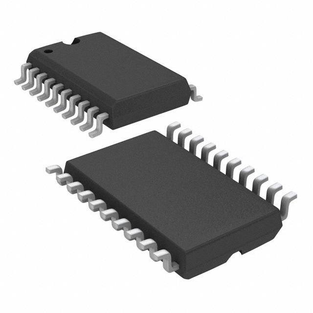
| 描述 | IC DVR/RCVR RS232 ESD 20SOIC |
| 产品分类 | |
| 品牌 | Texas Instruments |
| 数据手册 | |
| 产品图片 |
|
| 产品型号 | TRS3223ECDWR |
| rohs | 无铅 / 符合限制有害物质指令(RoHS)规范要求 |
| 产品系列 | - |
| 产品目录页面 | |
| 供应商器件封装 | 20-SOIC |
| 其它名称 | 296-25027-1 |
| 包装 | 剪切带 (CT) |
| 协议 | RS232 |
| 双工 | 全 |
| 安装类型 | 表面贴装 |
| 封装/外壳 | 20-SOIC(0.295",7.50mm 宽) |
| 工作温度 | 0°C ~ 70°C |
| 接收器滞后 | 500mV |
| 数据速率 | 500kbps |
| 标准包装 | 1 |
| 电压-电源 | 3 V ~ 5.5 V |
| 类型 | 收发器 |
| 驱动器/接收器数 | 2/2 |


- 商务部:美国ITC正式对集成电路等产品启动337调查
- 曝三星4nm工艺存在良率问题 高通将骁龙8 Gen1或转产台积电
- 太阳诱电将投资9.5亿元在常州建新厂生产MLCC 预计2023年完工
- 英特尔发布欧洲新工厂建设计划 深化IDM 2.0 战略
- 台积电先进制程称霸业界 有大客户加持明年业绩稳了
- 达到5530亿美元!SIA预计今年全球半导体销售额将创下新高
- 英特尔拟将自动驾驶子公司Mobileye上市 估值或超500亿美元
- 三星加码芯片和SET,合并消费电子和移动部门,撤换高东真等 CEO
- 三星电子宣布重大人事变动 还合并消费电子和移动部门
- 海关总署:前11个月进口集成电路产品价值2.52万亿元 增长14.8%

PDF Datasheet 数据手册内容提取
TRS3223E 3-V TO 5.5-V MULTICHANNEL RS-232 LINE DRIVER/RECEIVER WITH – 15-kV ESD PROTECTION www.ti.com SLLS794–JUNE2007 FEATURES DB, DW, OR PW PACKAGE • ESDProtectionforRS-232BusPins (TOP VIEW) – – 15-kVHuman-BodyModel(HBM) – – 8-kVIEC61000-4-2,ContactDischarge EN 1 20 FORCEOFF – – 15-kVIEC61000-4-2,Air-GapDischarge C1+ 2 19 VCC V+ 3 18 GND • MeetsorExceedstheRequirementsof C1− 4 17 DOUT1 TIA/EIA-232-FandITUv.28Standards C2+ 5 16 RIN1 • OperatesWith3-Vto5.5-VV Supply C2− 6 15 ROUT1 CC • Operatesupto500kbit/s V− 7 14 FORCEON • TwoDriversandTwoReceivers DOUT2 8 13 DIN1 RIN2 9 12 DIN2 • LowStandbyCurrent...1μATyp ROUT2 10 11 INVALID • ExternalCapacitors...4· 0.1μF • Accepts5-VLogicInputWith3.3-VSupply • AlternativeHigh-SpeedPin-CompatibleDevice RHL PACKAGE (TOP VIEW) (1Mbit/s)forTRSF3223E F F O APPLICATIONS E C • Battery-PoweredSystems R N O • PDAs E F • Notebooks 1 24 • Laptops C1+ 2 23 VCC • PalmtopPCs N.C. 3 22 N.C. • Hand-HeldEquipment V+ 4 21 GND C1– 5 20 DOUT1 DESCRIPTION/ C2+ 6 19 RIN1 ORDERING INFORMATION C2– 7 18 ROUT1 V– 8 17 FORCEON The TRS3223E consists of two line drivers, two line DOUT2 9 16 DIN1 receivers, and a dual charge-pump circuit with – 15-kV ESD protection pin to pin (serial-port N.C. 10 15 N.C. RIN2 11 14 DIN2 connection pins, including GND). The device meets 12 13 the requirements of TIA/EIA-232-F and provides the 2 D electrical interface between an asynchronous UT ALI communication controller and the serial-port O V R N connector. The charge pump and four small external I capacitors allow operation from a single 3-V to 5.5-V N.C. − No internal connection supply. The device operates at typical data signaling rates up to 500 kbit/s and a maximum of 30-V/μs driveroutputslewrate. Flexible control options for power management are available when the serial port is inactive. The auto-powerdown feature functions when FORCEON is low and FORCEOFF is high. During this mode of operation, if the device does not sense a valid RS-232 signal, the driver outputs are disabled. If FORCEOFF is set low and EN is high, both drivers and receivers are shut off, and the supply current is reduced to 1 mA. Disconnecting the serial port or turning off the peripheral drivers causes auto-powerdown to occur. Auto-powerdown can be disabled when FORCEON and FORCEOFF are high. With auto-powerdown enabled, the device is activated automatically when a valid signal is applied to any receiver input. The INVALID output is used to notify the user if an RS-232 signal is present at any receiver input. INVALID is high (valid data) if any receiver input voltage is greater than 2.7 V or less than –2.7 V, or has been between –0.3 V and 0.3 V for less than 30 μs. INVALID is low (invalid data) if the receiver input voltage is between –0.3 V and 0.3 V for more than 30μs.RefertoFigure4forreceiverinputlevels. Pleasebeawarethatanimportantnoticeconcerningavailability,standardwarranty,anduseincriticalapplicationsofTexas Instrumentssemiconductorproductsanddisclaimerstheretoappearsattheendofthisdatasheet. UNLESS OTHERWISE NOTED this document contains Copyright©2007,TexasInstrumentsIncorporated PRODUCTION DATA information current as of publication date. Products conform to specifications per the terms of Texas Instruments standard warranty. Production processing does not necessarilyincludetestingofallparameters.
TRS3223E 3-V TO 5.5-V MULTICHANNEL RS-232 LINE DRIVER/RECEIVER WITH – 15-kV ESD PROTECTION www.ti.com SLLS794–JUNE2007 ORDERINGINFORMATION T PACKAGE(1)(2) ORDERABLEPARTNUMBER TOP-SIDEMARKING A QFN–RHL Reelof2000 TRS3223ECRHLR PREVIEW Tubeof25 TRS3223ECDW SOIC–DW TRS3223EC Reelof2000 TRS3223ECDWR 0(cid:176) Cto70(cid:176) C Tubeof70 TRS3223ECDB SSOP–DB RS23EC Reelof2000 TRS3223ECDBR Tubeof70 TRS3223ECPW TSSOP–PW RS23EC Reelof2000 TRS3223ECPWR QFN–RHL Reelof2000 TRS3223EIRHLR PREVIEW Tubeof25 TRS3223EIDW SOIC–DW TRS3223EI Reelof2000 TRS3223EIDWR –40(cid:176) Cto85(cid:176) C Tubeof70 TRS3223EIDB SSOP–DB RS23EI Reelof2000 TRS3223EIDBR Tubeof70 TRS3223EIPW TSSOP–PW RS23EI Reelof2000 TRS3223EIPWR (1) Packagedrawings,standardpackingquantities,thermaldata,symbolization,andPCBdesignguidelinesareavailableat www.ti.com/sc/package. (2) Forthemostcurrentpackageandorderinginformation,seethePackageOptionAddendumattheendofthisdocument,orseetheTI websiteatwww.ti.com. FUNCTIONTABLES ABC EACHDRIVER(1) INPUTS OUTPUT DIN FORCEON FORCEOFF VALIDRIN DOUT DRIVERSTATUS RS-232LEVEL X X L X Z Poweredoff L H H X H Normaloperationwith H H H X L auto-powerdowndisabled L L H Yes H Normaloperationwith H L H Yes L auto-powerdownenabled L L H No Z Poweredoffby H L H No Z auto-powerdownfeature (1) H=highlevel,L=lowlevel,X=irrelevant,Z=highimpedance EACHRECEIVER(1) INPUTS OUTPUT RIN EN VALIDRIN DOUT RS-232LEVEL L L X H H L X L X H X Z Open L No H (1) H=highlevel,L=lowlevel,X=irrelevant, Z=highimpedance(off), Open=inputdisconnectedorconnecteddriveroff 2 SubmitDocumentationFeedback
TRS3223E 3-V TO 5.5-V MULTICHANNEL RS-232 LINE DRIVER/RECEIVER WITH – 15-kV ESD PROTECTION www.ti.com SLLS794–JUNE2007 LOGICDIAGRAM(POSITIVELOGIC) 13 17 DIN1 DOUT1 12 8 DIN2 DOUT2 20 FORCEOFF 11 14 Powerdown INVALID FORCEON 1 EN 15 16 ROUT1 RIN1 10 9 ROUT2 RIN2 PinnumbersarefortheDB,DW,andPWpackages. Absolute Maximum Ratings(1) overoperatingfree-airtemperaturerange(unlessotherwisenoted) MIN MAX UNIT V Supplyvoltagerange –0.3 6 V CC V+ Positive-outputsupplyvoltagerange(2) –0.3 7 V V– Negative-outputsupplyvoltagerange(2) 0.3 –7 V V+–V– Supplyvoltagedifference(2) 13 V Driver(FORCEOFF,FORCEON,EN) –0.3 6 V Inputvoltagerange V I Receiver –25 25 Driver –13.2 13.2 V Outputvoltagerange V O Receiver(INVALID) –0.3 V +0.3 CC DBpackage 70 DWpackage 58 θ Packagethermalimpedance(3)(4) (cid:176) C/W JA PWpackage 83 RHLpackage PREVIEW T Operatingvirtualjunctiontemperature 150 (cid:176) C J T Storagetemperaturerange –65 150 (cid:176) C stg (1) Stressesbeyondthoselistedunder"absolutemaximumratings"maycausepermanentdamagetothedevice.Thesearestressratings only,andfunctionaloperationofthedeviceattheseoranyotherconditionsbeyondthoseindicatedunder"recommendedoperating conditions"isnotimplied.Exposuretoabsolute-maximum-ratedconditionsforextendedperiodsmayaffectdevicereliability. (2) AllvoltagesarewithrespecttonetworkGND. (3) MaximumpowerdissipationisafunctionofT(max),θ ,andT .Themaximumallowablepowerdissipationatanyallowableambient J JA A temperatureisP =(T(max)–T )/θ .OperatingattheabsolutemaximumT of150(cid:176) Ccanaffectreliability. D J A JA J (4) ThepackagethermalimpedanceiscalculatedinaccordancewithJESD51-7. SubmitDocumentationFeedback 3
TRS3223E 3-V TO 5.5-V MULTICHANNEL RS-232 LINE DRIVER/RECEIVER WITH – 15-kV ESD PROTECTION www.ti.com SLLS794–JUNE2007 Recommended Operating Conditions(1) SeeFigure6 MIN NOM MAX UNIT V =3.3V 3 3.3 3.6 CC Supplyvoltage V V =5V 4.5 5 5.5 CC Driverandcontrol VCC=3.3V 2 V DIN,EN,FORCEOFF,FORCEON V IH high-levelinputvoltage V =5V 2.4 CC Driverandcontrol V DIN,EN,FORCEOFF,FORCEON 0.8 V IL low-levelinputvoltage Driverandcontrolinputvoltage DIN,EN,FORCEOFF,FORCEON 0 5.5 V V I Receiverinputvoltage –25 25 V TRS3223EC 0 70 T Operatingfree-airtemperature (cid:176) C A TRS3223EI –40 85 (1) TestconditionsareC1–C4=0.1μFatV =3.3V– 0.3V;C1=0.047μF,C2–C4=0.33μFatV =5V– 0.5V. CC CC Electrical Characteristics(1) overrecommendedrangesofsupplyvoltageandoperatingfree-airtemperature(unlessotherwisenoted)(seeFigure5) PARAMETER TESTCONDITIONS MIN TYP(2) MAX UNIT I Inputleakage EN,FORCEOFF, – 0.01 – 1 μA I current FORCEON V =3.3Vor5V,T =25(cid:176) C, Auto-powerdowndisabled CC A 0.3 1 mA Noload,FORCEOFFandFORCEONatV CC I Supplycurrent Poweredoff Noload,FORCEOFFatGND 1 10 CC Noload,FORCEOFFatV ,FORCEONatGND, μA Auto-powerdownenabled CC 1 10 AllRINareopenorgrounded (1) TestconditionsareC1–C4=0.1μFatV =3.3V– 0.3V;C1=0.047μF,C2–C4=0.33μFatV =5V– 0.5V. CC CC (2) AlltypicalvaluesareatV =3.3VorV =5V,andT =25(cid:176) C. CC CC A 4 SubmitDocumentationFeedback
TRS3223E 3-V TO 5.5-V MULTICHANNEL RS-232 LINE DRIVER/RECEIVER WITH – 15-kV ESD PROTECTION www.ti.com SLLS794–JUNE2007 DRIVER SECTION Electrical Characteristics(1) overrecommendedrangesofsupplyvoltageandoperatingfree-airtemperature(unlessotherwisenoted)(seeFigure5) PARAMETER TESTCONDITIONS MIN TYP(2) MAX UNIT V High-leveloutputvoltage DOUTatR =3kW toGND 5 5.4 V OH L V Low-leveloutputvoltage DOUTatR =3kW toGND –5 –5.4 V OL L I High-levelinputcurrent V =V – 0.01 – 1 μA IH I CC I Low-levelinputcurrent V atGND – 0.01 – 1 μA IL I V =3.6V,V =0V I Short-circuitoutputcurrent(3) CC O – 35 – 60 mA OS V =5.5V,V =0V CC O r Outputresistance V ,V+,andV–=0V,V =– 2V 300 10M W o CC O FORCEOFF=GND,V =3Vto3.6V,V =– 12V – 25 CC O I Outputleakagecurrent μA OZ FORCEOFF=GND,V =4.5Vto5.5V,V =– 12V – 25 CC O (1) TestconditionsareC1–C4=0.1μFatV =3.3V– 0.3V;C1=0.047μF,C2–C4=0.33μFatV =5V– 0.5V. CC CC (2) AlltypicalvaluesareatV =3.3VorV =5V,andT =25(cid:176) C. CC CC A (3) Short-circuitdurationsshouldbecontrolledtopreventexceedingthedeviceabsolutepowerdissipationratings,andnotmorethanone outputshouldbeshortedatatime. Switching Characteristics(1) overrecommendedrangesofsupplyvoltageandoperatingfree-airtemperature(unlessotherwisenoted)(seeFigure5) PARAMETER TESTCONDITIONS MIN TYP(2) MAX UNIT C =1000pF, R =3kW , Maximumdatarate L L 250 500 kbit/s OneDOUTswitching, SeeFigure1 t Pulseskew(3) CL=150pFto2500pF, RL=3kW to7kW , 100 ns sk(p) SeeFigure2 SR(tr) Slewrate,transitionregion RL=3kW to7kW , CL=150pFto1000pF 6 30 V/μs (SeeFigure1) VCC=3.3V CL=150pFto2500pF 4 30 (1) TestconditionsareC1–C4=0.1μFatV =3.3V– 0.3V;C1=0.047μF,C2–C4=0.33μFatV =5V– 0.5V. CC CC (2) AlltypicalvaluesareatV =3.3VorV =5V,andT =25(cid:176) C. CC CC A (3) Pulseskewisdefinedas|t –t |ofeachchannelofthesamedevice. PLH PHL SubmitDocumentationFeedback 5
TRS3223E 3-V TO 5.5-V MULTICHANNEL RS-232 LINE DRIVER/RECEIVER WITH – 15-kV ESD PROTECTION www.ti.com SLLS794–JUNE2007 RECEIVER SECTION Electrical Characteristics(1) overrecommendedrangesofsupplyvoltageandoperatingfree-airtemperature(unlessotherwisenoted)(seeFigure6) PARAMETER TESTCONDITIONS MIN TYP(2) MAX UNIT V High-leveloutputvoltage I =–1mA V –0.6 V –0.1 V OH OH CC CC V Low-leveloutputvoltage I =1.6mA 0.4 V OL OL V =3.3V 1.6 2.4 CC V Positive-goinginputthresholdvoltage V IT+ V =5V 1.9 2.4 CC V =3.3V 0.6 1.1 CC V Negative-goinginputthresholdvoltage V IT– V =5V 0.6 1.4 CC V Inputhysteresis(V –V ) 0.5 V hys IT+ IT– I Outputleakagecurrent EN=V – 0.05 μA OZ CC r Inputresistance V =– 3Vto– 25V 3 5 kW i I (1) TestconditionsareC1–C4=0.1μFatV =3.3V– 0.3V;C1=0.047μF,C2–C4=0.33μFatV =5V– 0.5V. CC CC (2) AlltypicalvaluesareatV =3.3VorV =5V,andT =25(cid:176) C. CC CC A Switching Characteristics(1) overrecommendedrangesofsupplyvoltageandoperatingfree-airtemperature(unlessotherwisenoted) PARAMETER TESTCONDITIONS TYP(2) UNIT t Propagationdelaytime,low-tohigh-leveloutput C =150pF,SeeFigure3 150 ns PLH L t Propagationdelaytime,high-tolow-leveloutput C =150pF,SeeFigure3 150 ns PHL L t Outputenabletime C =150pF,R =3kW ,SeeFigure4 200 ns en L L t Outputdisabletime C =150pF,R =3kW ,SeeFigure4 200 ns dis L L t Pulseskew(3) SeeFigure3 50 ns sk(p) (1) TestconditionsareC1–C4=0.1μFatV =3.3V– 0.3V;C1=0.047μF,C2–C4=0.33μFatV =5V– 0.5V. CC CC (2) AlltypicalvaluesareatV =3.3VorV =5V,andT =25(cid:176) C. CC CC A (3) Pulseskewisdefinedas|t –t |ofeachchannelofthesamedevice. PLH PHL 6 SubmitDocumentationFeedback
TRS3223E 3-V TO 5.5-V MULTICHANNEL RS-232 LINE DRIVER/RECEIVER WITH – 15-kV ESD PROTECTION www.ti.com SLLS794–JUNE2007 AUTO-POWERDOWN SECTION Electrical Characteristics overrecommendedrangesofsupplyvoltageandoperatingfree-airtemperature(unlessotherwisenoted)(seeFigure5) PARAMETER TESTCONDITIONS MIN MAX UNIT Receiverinputthresholdfor V FORCEON=GND, FORCEOFF=V 2.7 V T+(valid) INVALIDhigh-leveloutputvoltage CC Receiverinputthresholdfor V FORCEON=GND, FORCEOFF=V –2.7 V T(valid) INVALIDhigh-leveloutputvoltage CC Receiverinputthresholdfor V FORCEON=GND, FORCEOFF=V –0.3 0.3 V T(invalid) INVALIDlow-leveloutputvoltage CC I =1mA, FORCEON=GND, V INVALIDhigh-leveloutputvoltage OH V –0.6 V OH FORCEOFF=V CC CC I =1.6mA, FORCEON=GND, V INVALIDlow-leveloutputvoltage OL 0.4 V OL FORCEOFF=V CC Switching Characteristics overrecommendedrangesofsupplyvoltageandoperatingfree-airtemperature(unlessotherwisenoted)(seeFigure5) PARAMETER TYP(1) UNIT t Propagationdelaytime,low-tohigh-leveloutput 1 μs valid t Propagationdelaytime,high-tolow-leveloutput 30 μs invalid t Supplyenabletime 100 μs en (1) AlltypicalvaluesareatV =3.3VorV =5V,andT =25(cid:176) C. CC CC A SubmitDocumentationFeedback 7
TRS3223E 3-V TO 5.5-V MULTICHANNEL RS-232 LINE DRIVER/RECEIVER WITH – 15-kV ESD PROTECTION www.ti.com SLLS794–JUNE2007 PARAMETER MEASUREMENT INFORMATION 3 V Input 1.5 V 1.5 V RS-232 0 V Generator Output (see Note B) 50 W CL RL (see Note A) tTHL tTLH FOR3C VEOFF Output 3 V 3 V VOH −3 V −3 V VOL TEST CIRCUIT VOLTAGE WAVEFORMS SR(tr)(cid:1) 6V t ort THL TLH A. C includesprobeandjigcapacitance. L B. Thepulsegeneratorhasthefollowingcharacteristics:PRR=250kbit/s,Z =50W ,50%dutycycle,t £ 10ns, O r t £ 10ns. f Figure1.DriverSlewRate 3 V RS-232 Input 1.5 V 1.5 V Output 0 V Generator 50 W (see Note B) RL C(sLe e Note A) tPHL tPLH VOH 3 V Output 50% 50% FORCEOFF VOL TEST CIRCUIT VOLTAGE WAVEFORMS A. C includesprobeandjigcapacitance. L B. Thepulsegeneratorhasthefollowingcharacteristics:PRR=250kbit/s,Z =50W ,50%dutycycle,t £ 10ns, O r t £ 10ns. f Figure2.DriverPulseSkew EN 3 V 0 V Input 1.5 V 1.5 V −3 V Output Generator (see Note B) 50 W tPHL tPLH CL (see Note A) VOH Output 50% 50% VOL TEST CIRCUIT VOLTAGE WAVEFORMS A. C includesprobeandjigcapacitance. L B. Thepulsegeneratorhasthefollowingcharacteristics:Z =50W ,50%dutycycle,t £ 10ns,t £ 10ns. O r f Figure3.ReceiverPropagationDelayTimes 8 SubmitDocumentationFeedback
TRS3223E 3-V TO 5.5-V MULTICHANNEL RS-232 LINE DRIVER/RECEIVER WITH – 15-kV ESD PROTECTION www.ti.com SLLS794–JUNE2007 PARAMETER MEASUREMENT INFORMATION (continued) VCC GND 3 V Input 1.5V 1.5V S1 0 V RL tPHZ tPZH (S1 at GND) (S1 at GND) 3 V or 0 V Output VOH CL Output 50% EN (see Note A) 0.3 V tPLZ Generator 50 W (S1 at VCC) (see Note B) 0.3 V Output 50% VOL tPZL TEST CIRCUIT (S1 at VCC) VOLTAGE WAVEFORMS A. C includesprobeandjigcapacitance. L B. Thepulsegeneratorhasthefollowingcharacteristics:Z =50W ,50%dutycycle,t £ 10ns,t £ 10ns. O r f Figure4.ReceiverEnableandDisableTimes SubmitDocumentationFeedback 9
TRS3223E 3-V TO 5.5-V MULTICHANNEL RS-232 LINE DRIVER/RECEIVER WITH – 15-kV ESD PROTECTION www.ti.com SLLS794–JUNE2007 PARAMETER MEASUREMENT INFORMATION (continued) 3 V 2.7 V 2.7 V EN Receiver 0 V Input 0 V ROUT −2.7 V 2.7 V −3 V Generator 50 W (see Note B) tinvalid tvalid VCC INVALID 50% VCC 50% VCC Output 0 V Auto- INVALID ten powerdown CL = 30 pF V+ ≈V+ (see Note A) 0.3 V Supply VCC FORCEOFF Voltages 0 V 0.3 V DIN DOUT FORCEON V− ≈V− TEST CIRCUIT VOLTAGE WAVEFORMS ÉÉÉÉÉÉÉÉÉÉÉÉ ÉÉVÉalid ÉRS-2É32 LÉeveÉl, INÉVALÉID HÉighÉÉ 2.7 V ÉÉÉÉÉÉÉÉÉÉÉÉ Indeterminate ÉÉÉÉÉÉÉÉÉÉÉÉ 0.3 V ÉÉÉÉIf SÉÉignaÉÉl ReÉÉmaiÉÉns WÉÉithinÉÉ ThÉÉis RÉÉegioÉÉn ÉÉ 0 V for More Than 30(cid:1)s, INVALID Is Low† ÉÉÉÉÉÉÉÉÉÉÉÉ 0.3 V ÉÉÉÉÉIndeÉtermÉinatÉe ÉÉÉÉ 2.7 ÉV ÉÉÉÉÉÉÉÉÉÉÉ Valid RS-232 Level, INVALID High ÉÉÉÉÉÉÉÉÉÉÉÉ †Auto-powerdown disables drivers and reduces supply current to 1 m A A. C includesprobeandjigcapacitance. L B. Thepulsegeneratorhasthefollowingcharacteristics:PRR=250kbit/s,Z =50W ,50%dutycycle,t £ 10ns, O r t £ 10ns. f Figure5.INVALIDPropagationDelayTimesandSupplyEnablingTime 10 SubmitDocumentationFeedback
TRS3223E 3-V TO 5.5-V MULTICHANNEL RS-232 LINE DRIVER/RECEIVER WITH – 15-kV ESD PROTECTION www.ti.com SLLS794–JUNE2007 APPLICATION INFORMATION 1 Auto- 20 EN Powerdown FORCEOFF 2 19 C1+ VCC CBYPASS = 0.1(cid:1)F + 3 18 C1 V+ GND C3† 4 C1 17 DOUT1 5 16 C2+ RIN1 + C2 6 15 C2 ROUT1 5 kW 7 14 V FORCEON C4 + 8 13 DOUT2 DIN1 9 12 RIN2 DIN2 10 11 ROUT2 INVALID 5 kW †C3 can be connected to VCC or GND. NOTES: A. Resistor values shown are nominal. B. Nonpolarized ceramic capacitors are acceptable. If polarized tantalum or electrolytic capacitors are used, they should be connected as shown. VCC vs CAPACITOR VALUES VCC C1 C2, C3, and C4 3.3 V (cid:1) 0.3 V 0.1 m F 0.1 m F 5 V (cid:1) 0.5 V 0.047 m F 0.33 m F 3 V to 5.5 V 0.1 m F 0.47 m F Figure6.TypicalOperatingCircuitandCapacitorValues SubmitDocumentationFeedback 11
PACKAGE OPTION ADDENDUM www.ti.com 6-Feb-2020 PACKAGING INFORMATION Orderable Device Status Package Type Package Pins Package Eco Plan Lead/Ball Finish MSL Peak Temp Op Temp (°C) Device Marking Samples (1) Drawing Qty (2) (6) (3) (4/5) TRS3223ECDBR ACTIVE SSOP DB 20 2000 Green (RoHS NIPDAU Level-1-260C-UNLIM 0 to 70 RS23EC & no Sb/Br) TRS3223ECDWR ACTIVE SOIC DW 20 2000 Green (RoHS NIPDAU Level-1-260C-UNLIM 0 to 70 TRS3223EC & no Sb/Br) TRS3223ECPW ACTIVE TSSOP PW 20 70 Green (RoHS NIPDAU Level-1-260C-UNLIM 0 to 70 RS23EC & no Sb/Br) TRS3223ECPWR ACTIVE TSSOP PW 20 2000 Green (RoHS NIPDAU Level-1-260C-UNLIM 0 to 70 RS23EC & no Sb/Br) TRS3223EIDB ACTIVE SSOP DB 20 70 Green (RoHS NIPDAU Level-1-260C-UNLIM -40 to 85 RS23EI & no Sb/Br) TRS3223EIDBR ACTIVE SSOP DB 20 2000 Green (RoHS NIPDAU Level-1-260C-UNLIM -40 to 85 RS23EI & no Sb/Br) TRS3223EIPW ACTIVE TSSOP PW 20 70 Green (RoHS NIPDAU Level-1-260C-UNLIM -40 to 85 RS23EI & no Sb/Br) TRS3223EIPWR ACTIVE TSSOP PW 20 2000 Green (RoHS NIPDAU Level-1-260C-UNLIM -40 to 85 RS23EI & no Sb/Br) (1) The marketing status values are defined as follows: ACTIVE: Product device recommended for new designs. LIFEBUY: TI has announced that the device will be discontinued, and a lifetime-buy period is in effect. NRND: Not recommended for new designs. Device is in production to support existing customers, but TI does not recommend using this part in a new design. PREVIEW: Device has been announced but is not in production. Samples may or may not be available. OBSOLETE: TI has discontinued the production of the device. (2) RoHS: TI defines "RoHS" to mean semiconductor products that are compliant with the current EU RoHS requirements for all 10 RoHS substances, including the requirement that RoHS substance do not exceed 0.1% by weight in homogeneous materials. Where designed to be soldered at high temperatures, "RoHS" products are suitable for use in specified lead-free processes. TI may reference these types of products as "Pb-Free". RoHS Exempt: TI defines "RoHS Exempt" to mean products that contain lead but are compliant with EU RoHS pursuant to a specific EU RoHS exemption. Green: TI defines "Green" to mean the content of Chlorine (Cl) and Bromine (Br) based flame retardants meet JS709B low halogen requirements of <=1000ppm threshold. Antimony trioxide based flame retardants must also meet the <=1000ppm threshold requirement. (3) MSL, Peak Temp. - The Moisture Sensitivity Level rating according to the JEDEC industry standard classifications, and peak solder temperature. (4) There may be additional marking, which relates to the logo, the lot trace code information, or the environmental category on the device. Addendum-Page 1
PACKAGE OPTION ADDENDUM www.ti.com 6-Feb-2020 (5) Multiple Device Markings will be inside parentheses. Only one Device Marking contained in parentheses and separated by a "~" will appear on a device. If a line is indented then it is a continuation of the previous line and the two combined represent the entire Device Marking for that device. (6) Lead/Ball Finish - Orderable Devices may have multiple material finish options. Finish options are separated by a vertical ruled line. Lead/Ball Finish values may wrap to two lines if the finish value exceeds the maximum column width. Important Information and Disclaimer:The information provided on this page represents TI's knowledge and belief as of the date that it is provided. TI bases its knowledge and belief on information provided by third parties, and makes no representation or warranty as to the accuracy of such information. Efforts are underway to better integrate information from third parties. TI has taken and continues to take reasonable steps to provide representative and accurate information but may not have conducted destructive testing or chemical analysis on incoming materials and chemicals. TI and TI suppliers consider certain information to be proprietary, and thus CAS numbers and other limited information may not be available for release. In no event shall TI's liability arising out of such information exceed the total purchase price of the TI part(s) at issue in this document sold by TI to Customer on an annual basis. Addendum-Page 2
PACKAGE MATERIALS INFORMATION www.ti.com 17-Aug-2012 TAPE AND REEL INFORMATION *Alldimensionsarenominal Device Package Package Pins SPQ Reel Reel A0 B0 K0 P1 W Pin1 Type Drawing Diameter Width (mm) (mm) (mm) (mm) (mm) Quadrant (mm) W1(mm) TRS3223ECDBR SSOP DB 20 2000 330.0 16.4 8.2 7.5 2.5 12.0 16.0 Q1 TRS3223ECDWR SOIC DW 20 2000 330.0 24.4 10.8 13.0 2.7 12.0 24.0 Q1 TRS3223ECPWR TSSOP PW 20 2000 330.0 16.4 6.95 7.1 1.6 8.0 16.0 Q1 TRS3223EIDBR SSOP DB 20 2000 330.0 16.4 8.2 7.5 2.5 12.0 16.0 Q1 TRS3223EIPWR TSSOP PW 20 2000 330.0 16.4 6.95 7.1 1.6 8.0 16.0 Q1 PackMaterials-Page1
PACKAGE MATERIALS INFORMATION www.ti.com 17-Aug-2012 *Alldimensionsarenominal Device PackageType PackageDrawing Pins SPQ Length(mm) Width(mm) Height(mm) TRS3223ECDBR SSOP DB 20 2000 367.0 367.0 38.0 TRS3223ECDWR SOIC DW 20 2000 367.0 367.0 45.0 TRS3223ECPWR TSSOP PW 20 2000 367.0 367.0 38.0 TRS3223EIDBR SSOP DB 20 2000 367.0 367.0 38.0 TRS3223EIPWR TSSOP PW 20 2000 367.0 367.0 38.0 PackMaterials-Page2
None
None
PACKAGE OUTLINE DW0020A SOIC - 2.65 mm max height SCALE 1.200 SOIC C 10.63 SEATING PLANE TYP 9.97 A PIN 1 ID 0.1 C AREA 18X 1.27 20 1 13.0 2X 12.6 11.43 NOTE 3 10 11 0.51 20X 7.6 0.31 2.65 MAX B 7.4 0.25 C A B NOTE 4 0.33 TYP 0.10 0.25 SEE DETAIL A GAGE PLANE 0.3 1.27 0 - 8 0.1 0.40 DETAIL A TYPICAL 4220724/A 05/2016 NOTES: 1. All linear dimensions are in millimeters. Dimensions in parenthesis are for reference only. Dimensioning and tolerancing per ASME Y14.5M. 2. This drawing is subject to change without notice. 3. This dimension does not include mold flash, protrusions, or gate burrs. Mold flash, protrusions, or gate burrs shall not exceed 0.15 mm per side. 4. This dimension does not include interlead flash. Interlead flash shall not exceed 0.43 mm per side. 5. Reference JEDEC registration MS-013. www.ti.com
EXAMPLE BOARD LAYOUT DW0020A SOIC - 2.65 mm max height SOIC 20X (2) SYMM 1 20 20X (0.6) 18X (1.27) SYMM (R0.05) TYP 10 11 (9.3) LAND PATTERN EXAMPLE SCALE:6X SOOPLEDNEINRG MASK METAL MSOELTDAEL RU NMDAESRK SOOPLEDNEINRG MASK 0.07 MAX 0.07 MIN ALL AROUND ALL AROUND NON SOLDER MASK SOLDER MASK DEFINED DEFINED SOLDER MASK DETAILS 4220724/A 05/2016 NOTES: (continued) 6. Publication IPC-7351 may have alternate designs. 7. Solder mask tolerances between and around signal pads can vary based on board fabrication site. www.ti.com
EXAMPLE STENCIL DESIGN DW0020A SOIC - 2.65 mm max height SOIC 20X (2) SYMM 1 20 20X (0.6) 18X (1.27) SYMM 10 11 (9.3) SOLDER PASTE EXAMPLE BASED ON 0.125 mm THICK STENCIL SCALE:6X 4220724/A 05/2016 NOTES: (continued) 8. Laser cutting apertures with trapezoidal walls and rounded corners may offer better paste release. IPC-7525 may have alternate design recommendations. 9. Board assembly site may have different recommendations for stencil design. www.ti.com
PACKAGE OUTLINE DB0020A SSOP - 2 mm max height SCALE 2.000 SMALL OUTLINE PACKAGE C 8.2 TYP 7.4 A 0.1 C PIN 1 INDEX AREA SEATING PLANE 18X 0.65 20 1 2X 7.5 5.85 6.9 NOTE 3 10 11 0.38 20X 0.22 5.6 B 0.1 C A B 5.0 NOTE 4 2 MAX (0.15) TYP 0.25 SEE DETAIL A GAGE PLANE 0 -8 0.95 0.05 MIN 0.55 DETA 15AIL A TYPICAL 4214851/B 08/2019 NOTES: 1. All linear dimensions are in millimeters. Any dimensions in parenthesis are for reference only. Dimensioning and tolerancing per ASME Y14.5M. 2. This drawing is subject to change without notice. 3. This dimension does not include mold flash, protrusions, or gate burrs. Mold flash, protrusions, or gate burrs shall not exceed 0.15 mm per side. 4. This dimension does not include interlead flash. Interlead flash shall not exceed 0.25 mm per side. 5. Reference JEDEC registration MO-150. www.ti.com
EXAMPLE BOARD LAYOUT DB0020A SSOP - 2 mm max height SMALL OUTLINE PACKAGE 20X (1.85) SYMM (R0.05) TYP 1 20X (0.45) 20 SYMM 18X (0.65) 10 11 (7) LAND PATTERN EXAMPLE EXPOSED METAL SHOWN SCALE: 10X SOLDER MASK METAL METAL UNDER SOLDER MASK OPENING SOLDER MASK OPENING EXPOSED METAL EXPOSED METAL 0.07 MAX 0.07 MIN ALL AROUND ALL AROUND NON-SOLDER MASK SOLDER MASK DEFINED DEFINED (PREFERRED) SOLDE15.000 R MASK DETAILS 4214851/B 08/2019 NOTES: (continued) 6. Publication IPC-7351 may have alternate designs. 7. Solder mask tolerances between and around signal pads can vary based on board fabrication site. www.ti.com
EXAMPLE STENCIL DESIGN DB0020A SSOP - 2 mm max height SMALL OUTLINE PACKAGE 20X (1.85) SYMM (R0.05) TYP 1 20X (0.45) 20 SYMM 18X (0.65) 10 11 (7) SOLDER PASTE EXAMPLE BASED ON 0.125 mm THICK STENCIL SCALE: 10X 4214851/B 08/2019 NOTES: (continued) 8. Laser cutting apertures with trapezoidal walls and rounded corners may offer better paste release. IPC-7525 may have alternate design recommendations. 9. Board assembly site may have different recommendations for stencil design. www.ti.com
IMPORTANTNOTICEANDDISCLAIMER TI PROVIDES TECHNICAL AND RELIABILITY DATA (INCLUDING DATASHEETS), DESIGN RESOURCES (INCLUDING REFERENCE DESIGNS), APPLICATION OR OTHER DESIGN ADVICE, WEB TOOLS, SAFETY INFORMATION, AND OTHER RESOURCES “AS IS” AND WITH ALL FAULTS, AND DISCLAIMS ALL WARRANTIES, EXPRESS AND IMPLIED, INCLUDING WITHOUT LIMITATION ANY IMPLIED WARRANTIES OF MERCHANTABILITY, FITNESS FOR A PARTICULAR PURPOSE OR NON-INFRINGEMENT OF THIRD PARTY INTELLECTUAL PROPERTY RIGHTS. These resources are intended for skilled developers designing with TI products. You are solely responsible for (1) selecting the appropriate TI products for your application, (2) designing, validating and testing your application, and (3) ensuring your application meets applicable standards, and any other safety, security, or other requirements. These resources are subject to change without notice. TI grants you permission to use these resources only for development of an application that uses the TI products described in the resource. Other reproduction and display of these resources is prohibited. No license is granted to any other TI intellectual property right or to any third party intellectual property right. TI disclaims responsibility for, and you will fully indemnify TI and its representatives against, any claims, damages, costs, losses, and liabilities arising out of your use of these resources. TI’s products are provided subject to TI’s Terms of Sale (www.ti.com/legal/termsofsale.html) or other applicable terms available either on ti.com or provided in conjunction with such TI products. TI’s provision of these resources does not expand or otherwise alter TI’s applicable warranties or warranty disclaimers for TI products. Mailing Address: Texas Instruments, Post Office Box 655303, Dallas, Texas 75265 Copyright © 2020, Texas Instruments Incorporated