ICGOO在线商城 > 集成电路(IC) > 接口 - 驱动器,接收器,收发器 > TRS208IDBR
 Datasheet下载
- 型号: TRS208IDBR
- 制造商: Texas Instruments
- 库位|库存: xxxx|xxxx
- 要求:
| 数量阶梯 | 香港交货 | 国内含税 |
| +xxxx | $xxxx | ¥xxxx |
查看当月历史价格
查看今年历史价格
TRS208IDBR产品简介:
ICGOO电子元器件商城为您提供TRS208IDBR由Texas Instruments设计生产,在icgoo商城现货销售,并且可以通过原厂、代理商等渠道进行代购。 TRS208IDBR价格参考¥5.93-¥13.33。Texas InstrumentsTRS208IDBR封装/规格:接口 - 驱动器,接收器,收发器, 全 收发器 4/4 RS232 24-SSOP。您可以下载TRS208IDBR参考资料、Datasheet数据手册功能说明书,资料中有TRS208IDBR 详细功能的应用电路图电压和使用方法及教程。
Texas Instruments(德州仪器)的型号TRS208IDBR属于接口类别的驱动器、接收器和收发器产品。该器件主要应用于需要高速数据传输和信号转换的场景,以下是其典型应用场景:

1. 工业自动化
   TRS208IDBR可用于工业通信协议中,例如RS-485或CAN总线通信。它支持多点通信,适用于工厂自动化设备、传感器网络和分布式控制系统中的数据交换。

2. 通信设备
   在通信基础设施中,该收发器可以用于调制解调器、路由器、网关和其他需要长距离、低噪声数据传输的设备。其差分信号特性能够有效降低电磁干扰(EMI),确保数据传输的可靠性。

3. 汽车电子系统
   虽然TRS208IDBR并非专门针对汽车级应用设计,但在非关键性车载通信模块中仍可使用,例如车内娱乐系统、诊断接口或辅助驾驶系统的低速数据链路。

4. 消费电子产品
   一些消费类设备(如打印机、扫描仪、POS机等)可能需要与外部设备进行串行通信,TRS208IDBR可以作为接口芯片实现这种功能,提供稳定的数据传输性能。

5. 楼宇自动化
   在楼宇管理系统中,该收发器可用于连接温控器、照明控制器和其他环境监测设备,支持高效且可靠的信号传递。

6. 医疗设备
   对于某些需要稳定数据传输的医疗设备(如监护仪、分析仪等),TRS208IDBR可以提供精确的信号处理能力,确保设备运行的准确性。

总之,TRS208IDBR凭借其高性能的差分驱动和接收能力,适合多种需要可靠数据传输的应用场景,特别是在长距离、多节点通信环境中表现出色。
| 参数 | 数值 |
| 产品目录 | 集成电路 (IC) |
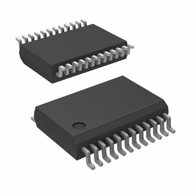
| 描述 | IC DVR/RCVR RS232 ESD 24SSOP |
| 产品分类 | |
| 品牌 | Texas Instruments |
| 数据手册 | |
| 产品图片 |
|
| 产品型号 | TRS208IDBR |
| rohs | 无铅 / 符合限制有害物质指令(RoHS)规范要求 |
| 产品系列 | - |
| 产品目录页面 | |
| 供应商器件封装 | 24-SSOP |
| 其它名称 | 296-24998-6 |
| 包装 | Digi-Reel® |
| 协议 | RS232 |
| 双工 | 全 |
| 安装类型 | 表面贴装 |
| 封装/外壳 | 24-SSOP(0.209",5.30mm 宽) |
| 工作温度 | -40°C ~ 85°C |
| 接收器滞后 | 500mV |
| 数据速率 | 120Kbps |
| 标准包装 | 1 |
| 电压-电源 | 4.5 V ~ 5.5 V |
| 类型 | 收发器 |
| 驱动器/接收器数 | 4/4 |


- 商务部:美国ITC正式对集成电路等产品启动337调查
- 曝三星4nm工艺存在良率问题 高通将骁龙8 Gen1或转产台积电
- 太阳诱电将投资9.5亿元在常州建新厂生产MLCC 预计2023年完工
- 英特尔发布欧洲新工厂建设计划 深化IDM 2.0 战略
- 台积电先进制程称霸业界 有大客户加持明年业绩稳了
- 达到5530亿美元!SIA预计今年全球半导体销售额将创下新高
- 英特尔拟将自动驾驶子公司Mobileye上市 估值或超500亿美元
- 三星加码芯片和SET,合并消费电子和移动部门,撤换高东真等 CEO
- 三星电子宣布重大人事变动 还合并消费电子和移动部门
- 海关总署:前11个月进口集成电路产品价值2.52万亿元 增长14.8%


PDF Datasheet 数据手册内容提取
TRS208 5-V MULTICHANNEL RS-232 LINE DRIVER/RECEIVER WITH – 15-kV ESD PROTECTION www.ti.com SLLS810–JULY2007 FEATURES • ESDProtectionforRS-232I/OPins DB, DW, OR NT PACKAGE – – 15-kVHuman-BodyModel(HBM) (TOPVIEW) • MeetsorExceedstheRequirementsof DOUT2 1 24 DOUT3 TIA/EIA-232-FandITUv.28Standards DOUT1 2 23 RIN3 • Operatesat5-VV Supply CC RIN2 3 22 ROUT3 • FourDriversandFourReceivers ROUT2 4 21 DIN4 • Operatesupto120kbit/s DIN1 5 20 DOUT4 • ExternalCapacitors...4· 0.1μF ROUT1 6 19 DIN3 • Latch-UpPerformanceExceeds100mAPer RIN1 7 18 DIN2 GND 8 17 ROUT4 JESD78,ClassII VCC 9 16 RIN4 APPLICATIONS C1+ 10 15 V- • Battery-PoweredSystems V+ 11 14 C2- C1- 12 13 C2+ • PDAs • Notebooks • Laptops • PalmtopPCs • Hand-HeldEquipment DESCRIPTION/ORDERING INFORMATION The TRS208 device consists of four line drivers, four line receivers, and a dual charge-pump circuit with – 15-kV HBM ESD protection pin to pin (serial-port connection pins, including GND). The device meets the requirements of TIA/EIA-232-F and provides the electrical interface between an asynchronous communication controller and the serial-port connector. The charge pump and four small external capacitors allow operation from a single 5-V supply. The devices operate at data signaling rates up to 120 kbit/s and a maximum of 30-V/μs driver output slewrate. ORDERINGINFORMATION T PACKAGE(1)(2) ORDERABLEPARTNUMBER TOP-SIDEMARKING A PDIP–NT Tubeof15 TRS208CNT PREVIEW Tubeof25 TRS208CDW SOIC–DW TRS208C 0(cid:176) Cto70(cid:176) C Reelof2000 TRS208CDWR Tubeof60 TRS208CDB SSOP–DB RU08C Reelof2000 TRS208CDBR PDIP–NT Tubeof15 TRS208INT PREVIEW Tubeof25 TRS208IDW SOIC–DW TRS208I –40(cid:176) Cto85(cid:176) C Reelof2000 TRS208IDWR Tubeof60 TRS208IDB SSOP–DB RU08I Reelof2000 TRS208IDBR (1) Packagedrawings,standardpackingquantities,thermaldata,symbolization,andPCBdesignguidelinesareavailableat www.ti.com/sc/package. (2) Forthemostcurrentpackageandorderinginformation,seethePackageOptionAddendumattheendofthisdocument,orseetheTI websiteatwww.ti.com. Pleasebeawarethatanimportantnoticeconcerningavailability,standardwarranty,anduseincriticalapplicationsofTexas Instrumentssemiconductorproductsanddisclaimerstheretoappearsattheendofthisdatasheet. UNLESS OTHERWISE NOTED this document contains Copyright©2007,TexasInstrumentsIncorporated PRODUCTION DATA information current as of publication date. Products conform to specifications per the terms of Texas Instruments standard warranty. Production processing does not necessarilyincludetestingofallparameters.
TRS208 5-V MULTICHANNEL RS-232 LINE DRIVER/RECEIVER WITH – 15-kV ESD PROTECTION www.ti.com SLLS810–JULY2007 FUNCTIONTABLES XXX EachDriver(1) INPUT OUTPUT DIN DOUT L H H L (1) H=highlevel,L=lowlevel EachReceiver(1) INPUT OUTPUT RIN ROUT L H H L Open H (1) H=highlevel,L=lowlevel, Open=inputdisconnectedor connecteddriveroff LOGICDIAGRAM(POSITIVELOGIC) 5 2 DIN1 DOUT1 18 1 DIN2 DOUT2 TTL/CMOS RS-232 Inputs Outputs 19 24 DIN3 DOUT3 21 20 DIN4 DOUT4 6 7 ROUT1 RIN1 4 3 ROUT2 RIN2 TTL/CMOS RS-232 Outputs 22 23 Inputs ROUT3 RIN3 17 16 ROUT4 RIN4 2 SubmitDocumentationFeedback
TRS208 5-V MULTICHANNEL RS-232 LINE DRIVER/RECEIVER WITH – 15-kV ESD PROTECTION www.ti.com SLLS810–JULY2007 Absolute Maximum Ratings(1) overoperatingfree-airtemperaturerange(unlessotherwisenoted) MIN MAX UNIT V Supplyvoltagerange(2) –0.3 6 V CC V+ Positivechargepumpvoltagerange(2) V –0.3 14 V CC V– Negativechargepumpvoltagerange(2) –14 0.3 V V+–V– Supplyvoltagedifference(2) 13 V Drivers –0.3 V++0.3 V Inputvoltagerange V I Receivers – 30 Drivers V––0.3 V++0.3 V Outputvoltagerange V O Receivers –0.3 V +0.3 CC Short-circuitduration DOUT Continuous DBpackage(3)(4) 63 θ Packagethermalimpedance DWpackage(3)(4) 46 (cid:176) C/W JA NTpackage(3)(5) 67 T Operatingvirtualjunctiontemperature 150 (cid:176) C J T Storagetemperaturerange –65 150 (cid:176) C stg (1) Stressesbeyondthoselistedunder"absolutemaximumratings"maycausepermanentdamagetothedevice.Thesearestressratings only,andfunctionaloperationofthedeviceattheseoranyotherconditionsbeyondthoseindicatedunder"recommendedoperating conditions"isnotimplied.Exposuretoabsolute-maximum-ratedconditionsforextendedperiodsmayaffectdevicereliability. (2) AllvoltagesarewithrespecttonetworkGND. (3) MaximumpowerdissipationisafunctionofT(max),θ ,andT .Themaximumallowablepowerdissipationatanyallowableambient J JA A temperatureisP =(T(max)–T )/θ .OperatingattheabsolutemaximumT of150(cid:176) Ccanaffectreliability. D J A JA J (4) ThepackagethermalimpedanceiscalculatedinaccordancewithJESD51-7. (5) ThepackagethermalimpedanceiscalculatedinaccordancewithJESD51-3. Recommended Operating Conditions(1) SeeFigure4 MIN NOM MAX UNIT Supplyvoltage 4.5 5 5.5 V V Driverhigh-levelinputvoltage DIN 2 V IH V Driverlow-levelinputvoltage DIN 0.8 V IL Driverinputvoltage DIN 0 5.5 V V I Receiverinputvoltage –30 30 TRS208C 0 70 T Operatingfree-airtemperature (cid:176) C A TRS208I –40 85 (1) TestconditionsareC1–C4=0.1μFatV =5V– 0.5V. CC Electrical Characteristics(1) overrecommendedrangesofsupplyvoltageandoperatingfree-airtemperature(unlessotherwisenoted)(seeFigure4) PARAMETER TESTCONDITIONS MIN TYP MAX UNIT I Supplycurrent Noload, V =5V, T =25(cid:176) C 11 20 mA CC CC A (1) TestconditionsareC1–C4=0.1μFatV =5V– 0.5V. CC SubmitDocumentationFeedback 3
TRS208 5-V MULTICHANNEL RS-232 LINE DRIVER/RECEIVER WITH – 15-kV ESD PROTECTION www.ti.com SLLS810–JULY2007 DRIVER SECTION Electrical Characteristics(1) overrecommendedrangesofsupplyvoltageandoperatingfree-airtemperature(unlessotherwisenoted)(seeFigure4) PARAMETER TESTCONDITIONS MIN TYP(2) MAX UNIT V High-leveloutputvoltage DOUTatR =3kW toGND, DIN=GND 5 9 V OH L V Low-leveloutputvoltage DOUTatR =3kW toGND, DIN=V –5 –9 V OL L CC I High-levelinputcurrent V =V 15 200 μA IH I CC I Low-levelinputcurrent V at0V –15 –200 μA IL I I (3) Short-circuitoutputcurrent V =5.5V, V =0V – 10 – 60 mA OS CC O r Outputresistance V ,V+,andV–=0V, V =– 2V 300 W o CC O (1) TestconditionsareC1–C4=0.1μFatV =5V– 0.5V. CC (2) AlltypicalvaluesareatV =5V,andT =25(cid:176) C CC A (3) Short-circuitdurationsshouldbecontrolledtopreventexceedingthedeviceabsolutepowerdissipationratings,andnotmorethanone outputshouldbeshortedatatime. Switching Characteristics(1) overrecommendedrangesofsupplyvoltageandoperatingfree-airtemperature(unlessotherwisenoted)(seeFigure4) PARAMETER TESTCONDITIONS MIN TYP(2) MAX UNIT C =50pFto1000pF, R =3kW to7kW , Maximumdatarate L L 120 kbit/s OneDOUTswitching, SeeFigure1 Propagationdelaytime, C =2500pF, R =3kW , t L L 2 μs PLH(D) low-tohigh-leveloutput Alldriversloaded, SeeFigure1 Propagationdelaytime, C =2500pF, R =3kW , t L L 2 μs PHL(D) high-tolow-leveloutput Alldriversloaded, SeeFigure1 t Pulseskew(3) CL=150pFto2500pF, RL=3kW to7kW , 300 ns sk(p) SeeFigure2 Slewrate,transitionregion C =50pFto1000pF, R =3kW to7kW , SR(tr) L L 3 6 30 V/μs (seeFigure1) V =5V CC (1) TestconditionsareC1–C4=0.1μFatV =5V– 0.5V. CC (2) AlltypicalvaluesareatV =5V,andT =25(cid:176) C. CC A (3) Pulseskewisdefinedas|t –t |ofeachchannelofthesamedevice. PLH PHL ESD Protection PIN TESTCONDITIONS TYP UNIT DOUT,RIN Human-BodyModel(HBM) – 15 kV 4 SubmitDocumentationFeedback
TRS208 5-V MULTICHANNEL RS-232 LINE DRIVER/RECEIVER WITH – 15-kV ESD PROTECTION www.ti.com SLLS810–JULY2007 RECEIVER SECTION Electrical Characteristics(1) overrecommendedrangesofsupplyvoltageandoperatingfree-airtemperature(unlessotherwisenoted)(seeFigure4) PARAMETER TESTCONDITIONS MIN TYP MAX UNIT V High-leveloutputvoltage I =–1mA 3.5 V OH OH V Low-leveloutputvoltage I =1.6mA 0.4 V OL OL V Positive-goinginputthresholdvoltage V =5V, T =25(cid:176) C 1.7 2.4 V IT+ CC A V Negative-goinginputthresholdvoltage V =5V, T =25(cid:176) C 0.8 1.2 V IT– CC A V Inputhysteresis(V –V ) V =5V 0.2 0.5 1 V hys IT+ IT– CC r Inputresistance V =– 3Vto– 25V, V =5V, T =25(cid:176) C 3 5 7 kW i I CC A (1) TestconditionsareC1–C4=0.1μFatV =5V– 0.5V. CC Switching Characteristics(1) overrecommendedrangesofsupplyvoltageandoperatingfree-airtemperature(unlessotherwisenoted)(seeFigure3) PARAMETER TESTCONDITIONS MIN TYP(2) MAX UNIT t Propagationdelaytime,low-tohigh-leveloutput C =150pF 0.5 10 μs PLH(R) L t Propagationdelaytime,high-tolow-leveloutput C =150pF 0.5 10 μs PHL(R) L t Pulseskew(3) 300 ns sk(p) (1) TestconditionsareC1–C4=0.1μFatV =5V– 0.5V. CC (2) AlltypicalvaluesareatV =5V,andT =25(cid:176) C. CC A (3) Pulseskewisdefinedas|t –t |ofeachchannelofthesamedevice. PLH PHL SubmitDocumentationFeedback 5
TRS208 5-V MULTICHANNEL RS-232 LINE DRIVER/RECEIVER WITH – 15-kV ESD PROTECTION www.ti.com SLLS810–JULY2007 PARAMETER MEASUREMENT INFORMATION 3 V Input 1.5 V 1.5 V RS-232 0 V Output Generator (see Note B) 50W C t t L PHL(D) PLH (D) RL (see NoteA) V 3 V 3 V OH Output –3 V –3 V V OL TEST CIRCUIT 6 V VOLTAGE WAVEFORMS SR(tf) = t or t PHL(D) PLH (D) NOTES: A. C includes probe and jig capacitance. L B. The pulse generator has the following characteristics: PRR = 120 kbit/s, Z = 50W, 50% duty cycle, t £10 ns, t £10 ns. O r f Figure1.DriverSlewRate 3 V RS-232 Input 1.5 V 1.5 V Generator Output 0 V (see Note B) 50W C t t L PHL(D) PLH (D) RL (see NoteA) V OH Output 50% 50% V OL TEST CIRCUIT VOLTAGE WAVEFORMS NOTES: A. C includes probe and jig capacitance. L B. The pulse generator has the following characteristics: PRR = 120 kbit/s, Z = 50W, 50% duty cycle, t £10 ns, t £10 ns. O r f Figure2.DriverPulseSkew 3 V Input 1.5 V 1.5 V Output -3 V Generator (see Note B) 50W t t C PHL(R) PLH (R) L (see NoteA) V OH Output 50% 50% V OL TEST CIRCUIT VOLTAGE WAVEFORMS NOTES: A. C includes probe and jig capacitance. L B. The pulse generator has the following characteristics: Z = 50W, 50% duty cycle, t £10 ns, t £10 ns. O r f Figure3.ReceiverPropagationDelayTimes 6 SubmitDocumentationFeedback
TRS208 5-V MULTICHANNEL RS-232 LINE DRIVER/RECEIVER WITH – 15-kV ESD PROTECTION www.ti.com SLLS810–JULY2007 APPLICATION INFORMATION 1 24 DOUT2 DOUT3 2 23 DOUT1 RIN3 5 kW 3 22 RIN2 ROUT3 5 kW 5 V ROUT2 4 400 kW 21 DIN4 5 V 20 DOUT4 400 kW 5 V 5 DIN1 400 kW ROUT1 6 19 DIN3 5 V 400 kW 7 18 RIN1 DIN2 5 kW GND 8 17 ROUT4 + 16 0.1mF RIN4 – 5 kW 0.1mF 9 V 16 V CC 15 0.1mF – V– – + 6.3 V + 10 C1+ 14 C2– 11 V+ – 0.1mF + 16 V + 0.1mF 6.3 V – 12 C1– C2+ 13 NOTES: A. Resistor values shown are nominal. B. Non-polarized ceramic capacitors are acceptable. If polarized tantalum or electrolytic capacitors are used, they should be connected as shown. Figure4.TypicalOperatingCircuitandCapacitorValues SubmitDocumentationFeedback 7
TRS208 5-V MULTICHANNEL RS-232 LINE DRIVER/RECEIVER WITH – 15-kV ESD PROTECTION www.ti.com SLLS810–JULY2007 APPLICATION INFORMATION (continued) Capacitor Selection The capacitor type used for C1–C4 is not critical for proper operation. The TRS208 requires 0.1-μF capacitors, although capacitors up to 10 μF can be used without harm. Ceramic dielectrics are suggested for the 0.1-μF capacitors. When using the minimum recommended capacitor values, ensure that the capacitance value does not degrade excessively as the operating temperature varies. If in doubt, use capacitors with a larger (e.g., 2· ) nominal value. The capacitors' effective series resistance (ESR), which usually rises at low temperatures, influencestheamountofrippleonV+andV–. Uselargercapacitors(upto10μF)toreducetheoutputimpedanceatV+andV–. Bypass V to ground with at least 0.1 μF. In applications sensitive to power-supply noise generated by the CC charge pumps, decouple V to ground with a capacitor the same size as (or larger than) the charge-pump CC capacitors(C1–C4). Electrostatic Discharge (ESD) Protection TI TRS208 devices have standard ESD protection structures incorporated on the pins to protect against electrostatic discharges encountered during assembly and handling. In addition, the RS-232 bus pins (driver outputs and receiver inputs) of these devices have an extra level of ESD protection. Advanced ESD structures weredesignedtosuccessfullyprotectthesebuspinsagainstESDdischargeof– 15kVwhenpowereddown. ESD Test Conditions ESD testing is stringently performed by TI, based on various conditions and procedures. Please contact TI for a reliabilityreportthatdocumentstestsetup,methodology,andresults. Human-Body Model (HBM) The HBM of ESD testing is shown in Figure 5, while Figure 6 shows the current waveform that is generated duringadischarge into a low impedance. The model consists of a 100-pF capacitor, charged to the ESD voltage ofconcernandsubsequentlydischargedintotheDUTthrougha1.5-kW resistor. R D 1.5 kW V + CS DUT HBM - 100 pF Figure5.HBMESDTestCircuit 8 SubmitDocumentationFeedback
TRS208 5-V MULTICHANNEL RS-232 LINE DRIVER/RECEIVER WITH – 15-kV ESD PROTECTION www.ti.com SLLS810–JULY2007 APPLICATION INFORMATION (continued) 1.5 V = 2 kV HBM DUT = 10-V, 1-WZener Diode | 1.0 A - T U D I 0.5 0.0 0 50 100 150 200 Time - ns Figure6.TypicalHBMCurrentWaveform Machine Model (MM) The MM ESD test applies to all pins using a 200-pF capacitor with no discharge resistance. The purpose of the MM test is to simulate possible ESD conditions that can occur during the handling and assembly processes of manufacturing. In this case, ESD protection is required for all pins, not just RS-232 pins. However, after PC boardassembly,theMMtestnolongerisaspertinenttotheRS-232pins. SubmitDocumentationFeedback 9
PACKAGE OPTION ADDENDUM www.ti.com 6-Feb-2020 PACKAGING INFORMATION Orderable Device Status Package Type Package Pins Package Eco Plan Lead/Ball Finish MSL Peak Temp Op Temp (°C) Device Marking Samples (1) Drawing Qty (2) (6) (3) (4/5) TRS208CDB ACTIVE SSOP DB 24 60 Green (RoHS NIPDAU Level-1-260C-UNLIM 0 to 70 RU08C & no Sb/Br) TRS208CDBR ACTIVE SSOP DB 24 2000 Green (RoHS NIPDAU Level-1-260C-UNLIM 0 to 70 RU08C & no Sb/Br) TRS208CDWR ACTIVE SOIC DW 24 2000 Green (RoHS NIPDAU Level-1-260C-UNLIM 0 to 70 TRS208C & no Sb/Br) TRS208IDB ACTIVE SSOP DB 24 60 Green (RoHS NIPDAU Level-1-260C-UNLIM -40 to 85 RU08I & no Sb/Br) TRS208IDBR ACTIVE SSOP DB 24 2000 Green (RoHS NIPDAU Level-1-260C-UNLIM -40 to 85 RU08I & no Sb/Br) TRS208IDWR ACTIVE SOIC DW 24 2000 Green (RoHS NIPDAU Level-1-260C-UNLIM -40 to 85 TRS208I & no Sb/Br) (1) The marketing status values are defined as follows: ACTIVE: Product device recommended for new designs. LIFEBUY: TI has announced that the device will be discontinued, and a lifetime-buy period is in effect. NRND: Not recommended for new designs. Device is in production to support existing customers, but TI does not recommend using this part in a new design. PREVIEW: Device has been announced but is not in production. Samples may or may not be available. OBSOLETE: TI has discontinued the production of the device. (2) RoHS: TI defines "RoHS" to mean semiconductor products that are compliant with the current EU RoHS requirements for all 10 RoHS substances, including the requirement that RoHS substance do not exceed 0.1% by weight in homogeneous materials. Where designed to be soldered at high temperatures, "RoHS" products are suitable for use in specified lead-free processes. TI may reference these types of products as "Pb-Free". RoHS Exempt: TI defines "RoHS Exempt" to mean products that contain lead but are compliant with EU RoHS pursuant to a specific EU RoHS exemption. Green: TI defines "Green" to mean the content of Chlorine (Cl) and Bromine (Br) based flame retardants meet JS709B low halogen requirements of <=1000ppm threshold. Antimony trioxide based flame retardants must also meet the <=1000ppm threshold requirement. (3) MSL, Peak Temp. - The Moisture Sensitivity Level rating according to the JEDEC industry standard classifications, and peak solder temperature. (4) There may be additional marking, which relates to the logo, the lot trace code information, or the environmental category on the device. (5) Multiple Device Markings will be inside parentheses. Only one Device Marking contained in parentheses and separated by a "~" will appear on a device. If a line is indented then it is a continuation of the previous line and the two combined represent the entire Device Marking for that device. Addendum-Page 1
PACKAGE OPTION ADDENDUM www.ti.com 6-Feb-2020 (6) Lead/Ball Finish - Orderable Devices may have multiple material finish options. Finish options are separated by a vertical ruled line. Lead/Ball Finish values may wrap to two lines if the finish value exceeds the maximum column width. Important Information and Disclaimer:The information provided on this page represents TI's knowledge and belief as of the date that it is provided. TI bases its knowledge and belief on information provided by third parties, and makes no representation or warranty as to the accuracy of such information. Efforts are underway to better integrate information from third parties. TI has taken and continues to take reasonable steps to provide representative and accurate information but may not have conducted destructive testing or chemical analysis on incoming materials and chemicals. TI and TI suppliers consider certain information to be proprietary, and thus CAS numbers and other limited information may not be available for release. In no event shall TI's liability arising out of such information exceed the total purchase price of the TI part(s) at issue in this document sold by TI to Customer on an annual basis. Addendum-Page 2
PACKAGE MATERIALS INFORMATION www.ti.com 14-Feb-2019 TAPE AND REEL INFORMATION *Alldimensionsarenominal Device Package Package Pins SPQ Reel Reel A0 B0 K0 P1 W Pin1 Type Drawing Diameter Width (mm) (mm) (mm) (mm) (mm) Quadrant (mm) W1(mm) TRS208CDBR SSOP DB 24 2000 330.0 16.4 8.2 8.8 2.5 12.0 16.0 Q1 TRS208CDWR SOIC DW 24 2000 330.0 24.4 10.75 15.7 2.7 12.0 24.0 Q1 TRS208IDBR SSOP DB 24 2000 330.0 16.4 8.2 8.8 2.5 12.0 16.0 Q1 TRS208IDWR SOIC DW 24 2000 330.0 24.4 10.75 15.7 2.7 12.0 24.0 Q1 PackMaterials-Page1
PACKAGE MATERIALS INFORMATION www.ti.com 14-Feb-2019 *Alldimensionsarenominal Device PackageType PackageDrawing Pins SPQ Length(mm) Width(mm) Height(mm) TRS208CDBR SSOP DB 24 2000 367.0 367.0 38.0 TRS208CDWR SOIC DW 24 2000 350.0 350.0 43.0 TRS208IDBR SSOP DB 24 2000 367.0 367.0 38.0 TRS208IDWR SOIC DW 24 2000 350.0 350.0 43.0 PackMaterials-Page2
None
MECHANICAL DATA MSSO002E – JANUARY 1995 – REVISED DECEMBER 2001 DB (R-PDSO-G**) PLASTIC SMALL-OUTLINE 28 PINS SHOWN 0,38 0,65 0,15 M 0,22 28 15 0,25 0,09 5,60 8,20 5,00 7,40 Gage Plane 1 14 0,25 A 0°–(cid:1)8° 0,95 0,55 Seating Plane 2,00 MAX 0,05 MIN 0,10 PINS ** 14 16 20 24 28 30 38 DIM A MAX 6,50 6,50 7,50 8,50 10,50 10,50 12,90 A MIN 5,90 5,90 6,90 7,90 9,90 9,90 12,30 4040065/E 12/01 NOTES: A. All linear dimensions are in millimeters. B. This drawing is subject to change without notice. C. Body dimensions do not include mold flash or protrusion not to exceed 0,15. D. Falls within JEDEC MO-150 • POST OFFICE BOX 655303 DALLAS, TEXAS 75265
IMPORTANTNOTICEANDDISCLAIMER TI PROVIDES TECHNICAL AND RELIABILITY DATA (INCLUDING DATASHEETS), DESIGN RESOURCES (INCLUDING REFERENCE DESIGNS), APPLICATION OR OTHER DESIGN ADVICE, WEB TOOLS, SAFETY INFORMATION, AND OTHER RESOURCES “AS IS” AND WITH ALL FAULTS, AND DISCLAIMS ALL WARRANTIES, EXPRESS AND IMPLIED, INCLUDING WITHOUT LIMITATION ANY IMPLIED WARRANTIES OF MERCHANTABILITY, FITNESS FOR A PARTICULAR PURPOSE OR NON-INFRINGEMENT OF THIRD PARTY INTELLECTUAL PROPERTY RIGHTS. These resources are intended for skilled developers designing with TI products. You are solely responsible for (1) selecting the appropriate TI products for your application, (2) designing, validating and testing your application, and (3) ensuring your application meets applicable standards, and any other safety, security, or other requirements. These resources are subject to change without notice. TI grants you permission to use these resources only for development of an application that uses the TI products described in the resource. Other reproduction and display of these resources is prohibited. No license is granted to any other TI intellectual property right or to any third party intellectual property right. TI disclaims responsibility for, and you will fully indemnify TI and its representatives against, any claims, damages, costs, losses, and liabilities arising out of your use of these resources. TI’s products are provided subject to TI’s Terms of Sale (www.ti.com/legal/termsofsale.html) or other applicable terms available either on ti.com or provided in conjunction with such TI products. TI’s provision of these resources does not expand or otherwise alter TI’s applicable warranties or warranty disclaimers for TI products. Mailing Address: Texas Instruments, Post Office Box 655303, Dallas, Texas 75265 Copyright © 2020, Texas Instruments Incorporated