ICGOO在线商城 > 集成电路(IC) > PMIC - 稳压器 - 线性 > TPS7A4701RGWT
 Datasheet下载
- 型号: TPS7A4701RGWT
- 制造商: Texas Instruments
- 库位|库存: xxxx|xxxx
- 要求:
| 数量阶梯 | 香港交货 | 国内含税 |
| +xxxx | $xxxx | ¥xxxx |
查看当月历史价格
查看今年历史价格
TPS7A4701RGWT产品简介:
ICGOO电子元器件商城为您提供TPS7A4701RGWT由Texas Instruments设计生产,在icgoo商城现货销售,并且可以通过原厂、代理商等渠道进行代购。 TPS7A4701RGWT价格参考。Texas InstrumentsTPS7A4701RGWT封装/规格:PMIC - 稳压器 - 线性, Linear Voltage Regulator IC 1 Output 1A 20-VQFN (5x5)。您可以下载TPS7A4701RGWT参考资料、Datasheet数据手册功能说明书,资料中有TPS7A4701RGWT 详细功能的应用电路图电压和使用方法及教程。
TPS7A4701RGWT是Texas Instruments(德州仪器)推出的一款低噪声、高精度、低压差线性稳压器(LDO),属于PMIC-稳压器-线性类别。该器件广泛应用于对电源噪声敏感、要求高稳定性的电子系统中。

典型应用场景包括:
1. 高性能模拟电路:如精密放大器、数据转换器(ADC/DAC)和传感器信号调理电路,其超低噪声(约4.7µVRMS)和高电源抑制比(PSRR)可有效减少电源干扰,提升系统精度。
2. 音频设备:用于便携式音频播放器、专业音响设备等,为音频编解码器(CODEC)或耳机放大器提供干净电源,降低背景噪声,提高音质。
3. 医疗电子:在便携式医疗仪器(如心电图仪、血糖仪)中,确保供电稳定可靠,满足安全与精度要求。
4. 测试与测量仪器:为示波器、信号发生器等设备中的敏感模块供电,保障测量准确性。
5. 工业控制系统:用于PLC模块、传感器供电等,具备良好的负载调整率和温度稳定性。

TPS7A4701RGWT采用固定输出电压(3.3V),支持1A输出电流,具备软启动、过流保护和热关断功能,封装为VQFN(RGW),节省空间且利于散热,适用于紧凑型高可靠性设计。
| 参数 | 数值 |
| 产品目录 | 集成电路 (IC)半导体 |
| 描述 | IC REG LDO ADJ 1A 20VQFN低压差稳压器 36V 1A 4.17uVRMS RF LDO VTG Reg |
| DevelopmentKit | TPS7A4701EVM-094 |
| 产品分类 | |
| 品牌 | Texas Instruments |
| 产品手册 | |
| 产品图片 |
|
| rohs | 符合RoHS无铅 / 符合限制有害物质指令(RoHS)规范要求 |
| 产品系列 | 电源管理 IC,低压差稳压器,Texas Instruments TPS7A4701RGWT- |
| mouser_ship_limit | 该产品可能需要其他文件才能进口到中国。 |
| 数据手册 | |
| 产品型号 | TPS7A4701RGWT |
| PSRR/纹波抑制—典型值 | 78 dB |
| 产品 | Voltage Regulators |
| 产品种类 | 低压差稳压器 |
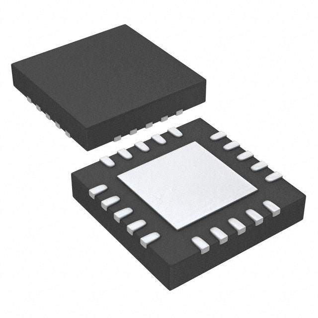
| 供应商器件封装 | 20-VQFN (5x5) |
| 其它名称 | 296-37243-1 |
| 制造商产品页 | http://www.ti.com/general/docs/suppproductinfo.tsp?distId=10&orderablePartNumber=TPS7A4701RGWT |
| 包装 | 剪切带 (CT) |
| 参考电压 | 1.4 V |
| 商标 | Texas Instruments |
| 回动电压—最大值 | 450 mV |
| 安装类型 | 表面贴装 |
| 安装风格 | SMD/SMT |
| 封装 | Reel |
| 封装/外壳 | 20-VQFN 裸露焊盘 |
| 封装/箱体 | VQFN-20 |
| 工作温度 | -40°C ~ 125°C |
| 工厂包装数量 | 250 |
| 最大工作温度 | + 125 C |
| 最大输入电压 | 36 V |
| 最小工作温度 | - 40 C |
| 最小输入电压 | 3 V |
| 标准包装 | 1 |
| 特色产品 | http://www.digikey.cn/product-highlights/zh/tps7a4701-rf-ldo-voltage-regulator/51915 |
| 电压-跌落(典型值) | 0.307V @ 1A |
| 电压-输入 | 3 V ~ 35 V |
| 电压-输出 | 1.4 V ~ 34 V |
| 电压调节准确度 | 2.5 % |
| 电流-输出 | 1A |
| 电流-限制(最小值) | 1A |
| 稳压器拓扑 | 正,可调式 |
| 稳压器数 | 1 |
| 类型 | RF LDO Regulator |
| 系列 | TPS7A4701 |
| 线路调整率 | 0.092 % |
| 负载调节 | 0.3 % |
| 输出电压 | 20.5 V |
| 输出电流 | 1 A |


- 商务部:美国ITC正式对集成电路等产品启动337调查
- 曝三星4nm工艺存在良率问题 高通将骁龙8 Gen1或转产台积电
- 太阳诱电将投资9.5亿元在常州建新厂生产MLCC 预计2023年完工
- 英特尔发布欧洲新工厂建设计划 深化IDM 2.0 战略
- 台积电先进制程称霸业界 有大客户加持明年业绩稳了
- 达到5530亿美元!SIA预计今年全球半导体销售额将创下新高
- 英特尔拟将自动驾驶子公司Mobileye上市 估值或超500亿美元
- 三星加码芯片和SET,合并消费电子和移动部门,撤换高东真等 CEO
- 三星电子宣布重大人事变动 还合并消费电子和移动部门
- 海关总署:前11个月进口集成电路产品价值2.52万亿元 增长14.8%


PDF Datasheet 数据手册内容提取
Product Sample & Technical Tools & Support & Folder Buy Documents Software Community TPS7A4700,TPS7A4701 SBVS204F–JUNE2012–REVISEDSEPTEMBER2014 TPS7A470x 36-V, 1-A, 4-µV , RF LDO Voltage Regulator RMS 1 Features 3 Description • InputVoltageRange:+3Vto+36V The TPS7A47 is a family of positive voltage (+36 V), 1 ultralow-noise (4 µV ) low-dropout linear regulators • OutputVoltageNoise: RMS (LDO)capableofsourcinga1-Aload. 4µV (10Hz,100kHz) RMS The TPS7A4700 output voltages are user- • Power-SupplyRippleRejection: programmable (up to 20.5 V) using a printed circuit – 82dB(100Hz) board (PCB) layout without the need of external – ≥ 55dB(10Hz,10MHz) resistors or feed-forward capacitors, thus reducing overallcomponentcount. • TwoOutputVoltageModes: – ANY-OUT™Version(User-Programmable The TPS7A4701 output voltage can be configured OutputviaPCBLayout): with a user-programmable PCB layout (up to 20.5 V), or adjustable (up to 34 V) with external feedback – NoExternalFeedbackResistorsorFeed- resistors. ForwardCapacitorsRequired The TPS7A47 is designed with bipolar technology – OutputVoltageRange:+1.4Vto+20.5V primarily for high-accuracy, high-precision – AdjustableVersion(TPS7A4701only): instrumentation applications where clean voltage rails – OutputVoltageRange:+1.4Vto+34V are critical to maximize system performance. This • OutputCurrent:1A feature makes the device ideal for powering operational amplifiers, analog-to-digital converters • DropoutVoltage:307mVat1A (ADCs), digital-to-analog converters (DACs), and • CMOSLogicLevel-CompatibleEnablePin other high-performance analog circuitry in critical • Built-InFixedCurrentLimitand applications such as medical, radio frequency (RF), ThermalShutdown andtest-and-measurement. • AvailableinHigh-PerformanceThermalPackage: In addition, the TPS7A47 is ideal for post dc-dc 5-mm×5-mmQFN converter regulation. By filtering out the output voltage ripple inherent to dc-dc switching • OperatingTemperatureRange: conversions, maximum system performance is –40°Cto125°C ensured in sensitive instrumentation, test-and- measurement,audio,andRFapplications. 2 Applications For applications where positive and negative low- • Voltage-ControlledOscillators(VCO) noiserailsarerequired,considerTI'sTPS7A33 family • FrequencySynthesizers of negative high-voltage, ultralow-noise linear • TestandMeasurement regulators. • Instrumentation,Medical,andAudio DeviceInformation(1) • RX,TX,andPACircuitry PARTNUMBER PACKAGE BODYSIZE(NOM) • SupplyRailsforOperationalAmplifiers, TPS7A470x VQFN(20) 5mm×5mm DACs,ADCs,andOtherHigh-PrecisionAnalog Circuitry (1) For all available packages, see the orderable addendum at theendofthedatasheet. • PostDC-DCConverterRegulationand RippleFiltering TPS7A47xx • BaseStationsandTelecomInfrastructure RF LDO • +12-Vand+24-VIndustrialBuses Amplifier TPS7A33 Negative-Voltage Regulator 1 An IMPORTANT NOTICE at the end of this data sheet addresses availability, warranty, changes, use in safety-critical applications, intellectualpropertymattersandotherimportantdisclaimers.PRODUCTIONDATA.
TPS7A4700,TPS7A4701 SBVS204F–JUNE2012–REVISEDSEPTEMBER2014 www.ti.com Table of Contents 1 Features.................................................................. 1 8 ApplicationandImplementation........................ 16 2 Applications........................................................... 1 8.1 ApplicationInformation............................................16 3 Description............................................................. 1 8.2 TypicalApplication .................................................16 4 RevisionHistory..................................................... 2 9 PowerSupplyRecommendations...................... 20 5 PinConfigurationandFunctions......................... 4 9.1 PowerDissipation(PD)...........................................20 6 Specifications......................................................... 5 10 Layout................................................................... 21 6.1 AbsoluteMaximumRatings......................................5 10.1 LayoutGuidelines.................................................21 6.2 HandlingRatings.......................................................6 10.2 LayoutExample....................................................21 6.3 RecommendedOperatingConditions.......................6 10.3 ThermalProtection................................................22 6.4 ThermalInformation..................................................6 10.4 EstimatingJunctionTemperature.........................22 6.5 ElectricalCharacteristics...........................................7 11 DeviceandDocumentationSupport................. 23 6.6 TypicalCharacteristics..............................................8 11.1 DocumentationSupport........................................23 7 DetailedDescription............................................ 12 11.2 RelatedLinks........................................................23 7.1 Overview.................................................................12 11.3 Trademarks...........................................................23 7.2 FunctionalBlockDiagram.......................................12 11.4 ElectrostaticDischargeCaution............................23 7.3 FeatureDescription.................................................12 11.5 Glossary................................................................23 7.4 DeviceFunctionalModes........................................13 12 Mechanical,Packaging,andOrderable Information........................................................... 23 7.5 Programming...........................................................13 4 Revision History NOTE:Pagenumbersforpreviousrevisionsmaydifferfrompagenumbersinthecurrentversion. ChangesfromRevisionE(January2014)toRevisionF Page • AddedHandlingRatingtable,FeatureDescriptionsection,DeviceFunctionalModes,Applicationand Implementationsection,PowerSupplyRecommendationssection,Layoutsection,DeviceandDocumentation Supportsection,andMechanical,Packaging,andOrderableInformationsection ............................................................... 1 • RewordedninthbulletinFeatureslist.................................................................................................................................... 1 • Changedpolarityofopampshownonrightsideofthefunctionalblockdiagram .............................................................. 12 • RewordedsecondparagraphinSoft-StartAndInrushCurrentsection .............................................................................. 13 • RevisedCapacitorRecommendationssection..................................................................................................................... 16 • Changedparagraph2ofDropoutVoltage(V )sectionforclarity ..................................................................................... 17 DO • Revisedparagraph1ofStartupsection .............................................................................................................................. 17 • Rewroteparagraph1ofPower-SupplyRejectionRatio(PSRR)sectiontoeliminateconfusion ........................................ 18 • Changedparagraph1ofPowerSupplyRecommendationssection................................................................................... 20 • Changedparagraph1andparagraph4ofPowerDissipation(P )section......................................................................... 20 D • Revisedparagraph2ofLayoutGuidelinessection ............................................................................................................. 21 • ChangedsecondparagraphofThermalProtectionsection ................................................................................................ 22 ChangesfromRevisionD(December2013)toRevisionE Page • ChangedOutputVoltageNoisevaluefrom4.17µVto4µVinthreeinstancesonfrontpage.............................................. 1 • Changed2ndand3rdparagraphsofDescriptionsection...................................................................................................... 1 • Added"ThermalPad"topinconfigurationdrawing................................................................................................................ 4 • ChangedENpindescription................................................................................................................................................... 4 • ChangedSENSE/FBpintobeforTPS7A4701only.............................................................................................................. 5 • AddednewrowtoPinDescriptionstableforSENSEpin(forTPS7A4700only)................................................................... 5 • AddednewrowtoPinDescriptionstableforthermalpad..................................................................................................... 5 • AddedV parameter............................................................................................................................................................ 7 REF 2 SubmitDocumentationFeedback Copyright©2012–2014,TexasInstrumentsIncorporated ProductFolderLinks:TPS7A4700 TPS7A4701
TPS7A4700,TPS7A4701 www.ti.com SBVS204F–JUNE2012–REVISEDSEPTEMBER2014 • AddedTPS7A4701devicetotestconditionsforV parameter............................................................................................ 7 NR • AddedFeedbackPinCurrentparametertoElectricalCharacteristics .................................................................................. 7 • DeletedDropoutVoltagevsOutputCurrentgraph................................................................................................................ 8 • AddedENpintoFunctionalBlockDiagram......................................................................................................................... 12 • AddedsentencetoANY-OUTProgrammableOutputVoltagesectiontoclarifyANY-OUTisforbothdevices.................. 13 • ChangedlasttwoparagraphsofAdjustableOperationsection........................................................................................... 14 • Added"TPS7A4701Only"toAdjustableOperationsectiontitle.......................................................................................... 14 • DeletedequationinFigure23.............................................................................................................................................. 14 • ChangedEquation3............................................................................................................................................................. 14 ChangesfromRevisionC(July2013)toRevisionD Page • Changeddatasheeetstatusfromproductionmixtoproductiondata.................................................................................... 1 • ChangedTPS7A4701ESDratingfrom>1kVto2.5kV....................................................................................................... 1 • Changednoisereductionpinvoltageparametertoshowbothdevices................................................................................. 7 • AddedtextclarifyingV typicalvaluetolastparagraphonpage...................................................................................... 14 REF ChangesfromRevisionB(April2013)toRevisionC Page • DeletedTPS7A4702previewdevicefromdatasheet............................................................................................................ 1 ChangesfromRevisionA(July2012)toRevisionB Page • ChangedTPS7A47toTPS7A4700........................................................................................................................................ 1 • AddedTPS7A4701andTPS7A4702previewdevicestodatasheet..................................................................................... 1 • Changedfront-pagefigure...................................................................................................................................................... 1 • AddedFBtoSENSEpintoFunctionalBlockDiagram........................................................................................................ 12 • AddednewparagraphafterTable1..................................................................................................................................... 14 • AddednewTable2............................................................................................................................................................... 14 • AddedAdjustableOperationsection.................................................................................................................................... 14 ChangesfromOriginal(June2012)toRevisionA Page • Movedtofullproductiondata(changesthroughoutdocument)............................................................................................. 1 Copyright©2012–2014,TexasInstrumentsIncorporated SubmitDocumentationFeedback 3 ProductFolderLinks:TPS7A4700 TPS7A4701
TPS7A4700,TPS7A4701 SBVS204F–JUNE2012–REVISEDSEPTEMBER2014 www.ti.com 5 Pin Configuration and Functions RGWPackage 5-mm×5-mmVQFN-20 (TopView) T U C C C O N N N N I 0 9 8 7 6 2 1 1 1 1 OUT 1 15 IN NC 2 14 NR SENSE/FB 3 13 EN 6P4V2 4 12 0P1V (Thermal Pad) 6P4V1 5 11 0P2V 6 7 8 9 10 V D V V V 2 N 6 8 4 P G P P P 3 1 0 0 PinFunctions PIN I/O DESCRIPTION NAME NO. WhenconnectedtoGND,thispinadds0.1Vtothenominaloutputvoltageoftheregulator. 0P1V 12 I DonotconnectanyvoltageotherthanGNDtothispin.Ifnotused,leavethispinfloating. WhenconnectedtoGND,thispinadds0.2Vtothenominaloutputvoltageoftheregulator. 0P2V 11 I DonotconnectanyvoltageotherthanGNDtothispin.Ifnotused,leavethispinfloating. WhenconnectedtoGND,thispinadds0.4Vtothenominaloutputvoltageoftheregulator. 0P4V 10 I DonotconnectanyvoltageotherthanGNDtothispin.Ifnotused,leavethispinfloating. WhenconnectedtoGND,thispinadds0.8Vtothenominaloutputvoltageoftheregulator. 0P8V 9 I DonotconnectanyvoltageotherthanGNDtothispin.Ifnotused,leavethispinfloating. WhenconnectedtoGND,thispinadds1.6Vtothenominaloutputvoltageoftheregulator. 1P6V 8 I DonotconnectanyvoltageotherthanGNDtothispin.Ifnotused,leavethispinfloating. WhenconnectedtoGND,thispinadds3.2Vtothenominaloutputvoltageoftheregulator. 3P2V 6 I DonotconnectanyvoltageotherthanGNDtothispin.Ifnotused,leavethispinfloating. WhenconnectedtoGND,thispinadds6.4Vtothenominaloutputvoltageoftheregulator. 6P4V1 5 I DonotconnectanyvoltageotherthanGNDtothispin.Ifnotused,leavethispinfloating. WhenconnectedtoGND,thispinadds6.4Vtothenominaloutputvoltageoftheregulator. 6P4V2 4 I DonotconnectanyvoltageotherthanGNDtothispin.Ifnotused,leavethispinfloating. Enablepin.Thedeviceisenabledwhenthevoltageonthispinexceedsthemaximum EN 13 I enablevoltage,V .Ifenableisnotrequired,tieENtoIN. EN(HI) GND 7 — Ground Inputsupply.Acapacitorgreaterthanorequalto1µFmustbetiedfromthispintogroundto assurestability. IN 15,16 I A10-µFcapacitorisrecommendedtobeconnectedfromINtoGND(asclosetothedevice aspossible)toreducecircuitsensitivitytoprintedcircuitboard(PCB)layout,especiallywhen longinputtracesorhighsourceimpedancesareencountered. NC 2,17-19 — ThispincanbeleftopenortiedtoanyvoltagebetweenGNDandIN. Noisereductionpin.WhenacapacitorisconnectedfromthispintoGND,RMSnoisecanbe reducedtoverylowlevels.Acapacitorgreaterthanorequalto10nFmustbetiedfromthis NR 14 — pintogroundtoassurestability.A1-µFcapacitorisrecommendedtobeconnectedfromNR toGND(asclosetothedeviceaspossible)tomaximizeacperformanceandminimizenoise. 4 SubmitDocumentationFeedback Copyright©2012–2014,TexasInstrumentsIncorporated ProductFolderLinks:TPS7A4700 TPS7A4701
TPS7A4700,TPS7A4701 www.ti.com SBVS204F–JUNE2012–REVISEDSEPTEMBER2014 PinFunctions(continued) PIN I/O DESCRIPTION NAME NO. Regulatoroutput.Acapacitorgreaterthanorequalto10µFmustbetiedfromthispinto groundtoassurestability.A47-µFceramicoutputcapacitorishighlyrecommendedtobe OUT 1,20 O connectedfromOUTtoGND(asclosetothedeviceaspossible)tomaximizeac performance. Control-looperroramplifierinput(TPS7A4701only). ThisistheSENSEpinifthedeviceoutputvoltageisprogrammedusingANY-OUT(no externalfeedbackresistors).ThispinmustbeconnectedtoOUT.Connectthispintothe SENSE/FB 3 I pointofloadtomaximizeaccuracy. ThisistheFBpinifthedeviceoutputvoltageissetusingexternalresistors.Seethe AdjustableOperationsectionformoredetails. Control-looperroramplifierinput(TPS7A4700only). SENSE 3 I ThisistheSENSEpinofthedeviceandmustbeconnectedtoOUT.Connectthispintothe pointofloadtomaximizeaccuracy. Connectthethermalpadtoalarge-areagroundplane.Thethermalpadisinternally ThermalPad — connectedtoGND. 6 Specifications 6.1 Absolute Maximum Ratings Overjunctiontemperaturerange,unlessotherwisenoted.(1) MIN MAX UNIT INpintoGNDpin –0.4 +36 V ENpintoGNDpin –0.4 +36 V ENpintoINpin –36 +0.4 V OUTpintoGNDpin –0.4 +36 V NRpintoGNDpin –0.4 +36 V SENSE/FBpintoGNDpin –0.4 +36 V 0P1VpintoGNDpin –0.4 +36 V Voltage(2) 0P2VpintoGNDpin –0.4 +36 V 0P4VpintoGNDpin –0.4 +36 V 0P8VpintoGNDpin –0.4 +36 V 1P6VpintoGNDpin –0.4 +36 V 3P2VpintoGNDpin –0.4 +36 V 6P4V1pintoGNDpin –0.4 +36 V 6P4V2pintoGNDpin –0.4 +36 V Current Peakoutput Internallylimited Temperature Operatingvirtualjunction,T –40 125 °C J (1) StressesbeyondthoselistedunderAbsoluteMaximumRatingsmaycausepermanentdamagetothedevice.Thesearestressratings only,whichdonotimplyfunctionaloperationofthedeviceattheseoranyotherconditionsbeyondthoseindicatedunderRecommended OperatingConditions.Exposuretoabsolute-maximum-ratedconditionsforextendedperiodsmayaffectdevicereliability.. (2) Allvoltagesarewithrespecttonetworkgroundterminal. Copyright©2012–2014,TexasInstrumentsIncorporated SubmitDocumentationFeedback 5 ProductFolderLinks:TPS7A4700 TPS7A4701
TPS7A4700,TPS7A4701 SBVS204F–JUNE2012–REVISEDSEPTEMBER2014 www.ti.com 6.2 Handling Ratings MIN MAX UNIT T Storagetemperaturerange –65 150 °C stg Humanbodymodel(HBM),per ANSI/ESDA/JEDECJS-001,allpins(1) –1000 1000 TPS7A4700 V Chargeddevicemodel(CDM),perJEDEC Electrostatic specificationJESD22-C101,allpins(2) –500 500 V (ESD) discharge Humanbodymodel(HBM),per ANSI/ESDA/JEDECJS-001,allpins(1) –2500 2500 TPS7A4701 V Chargeddevicemodel(CDM),perJEDEC specificationJESD22-C101,allpins(2) –500 500 (1) JEDECdocumentJEP155statesthat500-VHBMallowssafemanufacturingwithastandardESDcontrolprocess. (2) JEDECdocumentJEP157statesthat250-VCDMallowssafemanufacturingwithastandardESDcontrolprocess. 6.3 Recommended Operating Conditions overjunctiontemperaturerange(unlessotherwisenoted) MIN NOM MAX UNIT V 3.0 35.0 V I V 1.4 34.0 V O V 0 V V EN IN I 0 1.0 A O 6.4 Thermal Information TPS7A47xx THERMALMETRIC(1) RGW UNIT 20PINS R Junction-to-ambientthermalresistance 32.5 θJA R Junction-to-case(top)thermalresistance 27 θJC(top) R Junction-to-boardthermalresistance 11.9 θJB °C/W ψ Junction-to-topcharacterizationparameter 0.3 JT ψ Junction-to-boardcharacterizationparameter 11.9 JB R Junction-to-case(bottom)thermalresistance 1.7 θJC(bot) (1) Formoreinformationabouttraditionalandnewthermalmetrics,seetheICPackageThermalMetricsapplicationreport,SPRA953. 6 SubmitDocumentationFeedback Copyright©2012–2014,TexasInstrumentsIncorporated ProductFolderLinks:TPS7A4700 TPS7A4701
TPS7A4700,TPS7A4701 www.ti.com SBVS204F–JUNE2012–REVISEDSEPTEMBER2014 6.5 Electrical Characteristics At–40°C≤T ≤125°C;V =V +1.0VorV =3.0V(whicheverisgreater);V =V;I =0mA;C =10µF;C =10 J I O(nom) I EN I O IN OUT µF;C =10nF;SENSE/FBtiedtoOUT;and0P1V,0P2V,0P4V,0P8V,1P6V,3P2V,6P4V1,6P4V2pinsOPEN,unless NR otherwisenoted. PARAMETER TESTCONDITIONS MIN TYP MAX UNIT VI Inputvoltagerange 3 35 V VIrising 2.67 V VUVLO Under-voltagelockoutthreshold VIfalling 2.5 V V(REF) Referencevoltage V(REF)=V(FB),TPS7A4701only 1.4 V VUVLO(HYS) Under-voltagelockouthysteresis 177 mV TPS7A4700,TPS7A4701usingANY-OUT VNR Noisereductionpinvoltage option VOUT V TPS7A4701inadjustablemodeonly 1.4 V TPS7A4700, TPS7A4701 1.4 20.5 V usingANY- VI≥VO(nom)+1.0Vor3V OUToption Outputvoltagerange (whicheverisgreater), COUT=20µF TPS7A4701 VO uasdijnugstable 1.4 34 V option Nominalaccuracy TJ=25°C,COUT=20µF –1.0 1.0 %VO Overallaccuracy V0Om(nAom≤)+IO1≤.01VA≤,CVOIU≤T3=52V0,µF –2.5 2.5 %VO ΔVO(ΔVI) Lineregulation VO(nom)+1.0V≤VI≤35V 0.092 %VO ΔVO(ΔIO) Loadregulation 0mA≤IO≤1A 0.3 %VO VI=95%VO(nom),IO=0.5A 216 mV V(DO) Dropoutvoltage VI=95%VO(nom),IO=1A 307 450 mV I(CL) Currentlimit VO=90%VO(nom) 1 1.26 A IO=0mA 0.58 1.0 mA I(GND) Groundpincurrent IO=1A 6.1 mA VEN=VI 0.78 2 µA I(EN) Enablepincurrent VI=VEN=35V 0.81 2 µA VEN=0.4V 2.55 8 µA I(SHDN) Shutdownsupplycurrent VEN=0.4V,VI=35V 3.04 60 µA V+EN(HI) Enablehigh-levelvoltage 2.0 VI V V+EN(LO) Enablelow-levelvoltage 0.0 0.4 V I(FB) Feedbackpincurrent 350 nA PSRR Power-supplyrejectionratio VI=16V,VO(nom)=15V,COUT=50µF, 78 dB IO=500mA,CNR=1µF,f=1kHz VCIN=R3=V1,µVFO,(BnoWm)==110.4HVz,tCoO1U0T0=k5H0zµF, 4.17 µVRMS Vn Outputnoisevoltage VCINNR==61Vµ,FV,OB(nWom=)=105HV,zCtoOU1T00=k5H0zµF, 4.67 µVRMS Shutdown,temperatureincreasing 170 °C Tsd Thermalshutdowntemperature Reset,temperaturedecreasing 150 °C TJ Operatingjunctiontemperature –40 125 °C Copyright©2012–2014,TexasInstrumentsIncorporated SubmitDocumentationFeedback 7 ProductFolderLinks:TPS7A4700 TPS7A4701
TPS7A4700,TPS7A4701 SBVS204F–JUNE2012–REVISEDSEPTEMBER2014 www.ti.com 6.6 Typical Characteristics At–40°C≤T ≤125°C;V =V +1.0VorV =3.0V(whicheverisgreater);V =V;I =0mA;C =10µF;C =10 J I O(nom) I EN I O IN OUT µF;C =1µF;SENSE/FBtiedtoOUT;and0P1V,0P2V,0P4V,0P8V,1P6V,3P2V,6P4V1,6P4V2pinsOPEN,unless NR otherwisenoted. 100 4 VOUT = 1.4 V, VNOISE = 4.17 m VRMS −40°C VOUT = 5 V, VNOISE = 4.67 m VRMS 3 0°C VOUT = 10 V, VNOISE = 7.25 m VRMS +25°C 10 VOUT = 15 V, VNOISE = 12.28 m VRMS 2 +85°C Hz) %) 1 +125°C mNoise (V 1 ICCBOWONURUTR T==M = S15 N5 0Om00IFS mmEF (A10 Hz, 100 kHz) V (()OUTNOM −10 0.1 −2 −3 0.01 −4 10 100 1k 10k 100k 1M 0 5 10 15 20 25 30 35 40 Frequency (Hz) Input Voltage (V) G020 G001 Figure1.NoisevsOutputVoltage Figure2.LineRegulation 4 3 −40°C UVLO Threshold Off 2.9 3 0°C UVLO Threshold On +25°C 2.8 2 +85°C 2.7 %) 1 +125°C ()M V) 2.6 NO 0 (N 2.5 (OUT −1 VI 2.4 V 2.3 −2 2.2 −3 2.1 −4 2 0 100 200 300 400 500 600 700 800 900 1000 −40 −25 −10 5 20 35 50 65 80 95 110 125 Output Current (mA) Temperature (°C) G002 G004 Figure3.LoadRegulation Figure4.UVLOThresholdvsTemperature 3 1000 2.7 2.4 800 2.1 1.8 600 V) A) V (EN 11..25 I (µQ 400 −40°C 0.9 0°C 0.6 200 +25°C +105°C 0.3 IOUT = 0 m A +125°C 0 0 −40 −25 −10 5 20 35 50 65 80 95 110 125 0 5 10 15 20 25 30 35 40 Temperature (°C) Input Voltage (V) G005 G006 Figure5.EnableVoltageThresholdvsTemperature Figure6.QuiescentCurrentvsInputVoltage 8 SubmitDocumentationFeedback Copyright©2012–2014,TexasInstrumentsIncorporated ProductFolderLinks:TPS7A4700 TPS7A4701
TPS7A4700,TPS7A4701 www.ti.com SBVS204F–JUNE2012–REVISEDSEPTEMBER2014 Typical Characteristics (continued) At–40°C≤T ≤125°C;V =V +1.0VorV =3.0V(whicheverisgreater);V =V;I =0mA;C =10µF;C =10 J I O(nom) I EN I O IN OUT µF;C =1µF;SENSE/FBtiedtoOUT;and0P1V,0P2V,0P4V,0P8V,1P6V,3P2V,6P4V1,6P4V2pinsOPEN,unless NR otherwisenoted. 10 2.0 −40°C 1.8 0°C 1.6 +25°C +85°C 1.4 +125°C I (mA)GND 1 I (µA)EN 011...802 −40°C 0.6 0°C +25°C 0.4 +85°C 0.2 +125°C 0.1 0.0 1 10 100 1000 0 5 10 15 20 25 30 35 40 Output Current (mA) Input Voltage (V) G007 G008 Figure7.GroundCurrentvsOutputCurrent Figure8.EnableCurrentvsInputVoltage 10 3 9 −40°C VOUT = 90% VOUT(NOM) 0°C 2.5 8 +25°C +105°C 7 +125°C 2 A) 6 (µSHDN 45 I (A)CL 1.5 I 1 −40°C 3 0°C 2 +25°C 0.5 +85°C 1 +125°C 0 0 0 5 10 15 20 25 30 35 40 0 4 8 12 16 20 Input Voltage (V) Input Voltage (V) G009 G010 Figure9.ShutdownCurrentvsInputVoltage Figure10.CurrentLimitvsInputVoltage 100 100 90 90 80 80 70 70 B) 60 B) 60 d d R ( 50 R ( 50 R R S 40 S 40 P P 30 IOUT = 1 A CNR = 0.01 m F 30 CNR = 0.01 m F IOUT = 0.5 A 20 COUT = 50 m F CNR = 0.1 m F 20 CNR = 0.1 m F COUT = 50 m F 10 VVIONU =T =3 1V.4 V CCNNRR == 12 .m2 Fm F 10 CCNNRR == 12 .2m Fm F VVIONU =T =3 1V.4 V 0 0 10 100 1k 10k 100k 1M 10M 10 100 1k 10k 100k 1M 10M Frequency (Hz) Frequency (Hz) G011 G012 Figure11.Power-SupplyRejectionRatiovsC Figure12.Power-SupplyRejectionRatiovsC NR NR Copyright©2012–2014,TexasInstrumentsIncorporated SubmitDocumentationFeedback 9 ProductFolderLinks:TPS7A4700 TPS7A4701
TPS7A4700,TPS7A4701 SBVS204F–JUNE2012–REVISEDSEPTEMBER2014 www.ti.com Typical Characteristics (continued) At–40°C≤T ≤125°C;V =V +1.0VorV =3.0V(whicheverisgreater);V =V;I =0mA;C =10µF;C =10 J I O(nom) I EN I O IN OUT µF;C =1µF;SENSE/FBtiedtoOUT;and0P1V,0P2V,0P4V,0P8V,1P6V,3P2V,6P4V1,6P4V2pinsOPEN,unless NR otherwisenoted. 100 100 90 90 80 80 70 70 B) 60 B) 60 d d R ( 50 R ( 50 R R S 40 S 40 P P 30 CNR = 1 m F IOUT = 0 mA 30 VOUT = 3.3 V VDO = 200 mV 20 COUT = 50 m F IOUT = 50 mA 20 CNR = 1 m F VDO = 300 mV 10 VIN = 3 V IOUT = 500 mA 10 COUT = 50 m F VDO = 500 mV VOUT = 1.4 V IOUT = 1000 mA IOUT = 50 mA VDO = 1 V 0 0 10 100 1k 10k 100k 1M 10M 10 100 1k 10k 100k 1M 10M Frequency (Hz) Frequency (Hz) G013 G014 Figure13.Power-SupplyRejectionRatiovsI Figure14.Power-SupplyRejectionRatiovsDropout O 100 100 90 VDO = 200 mV VDO = 500 mV 90 VDO = 200 mV VDO = 500 mV VDO = 300 mV VDO = 1 V VDO = 300 mV VDO = 1 V 80 80 70 70 B) 60 B) 60 d d PSRR ( 345000 VCONURT = = 1 3 m.3F ,V C, IOOUUTT == 5500 0m FmA PSRR ( 345000 VCCIOONOUURUTT T== == 11 35 mA.03F mVF 20 20 10 10 0 0 10 100 1k 10k 100k 1M 10M 10 100 1k 10k 100k 1M 10M Frequency (Hz) Frequency (Hz) G015 G016 Figure15.Power-SupplyRejectionRatiovsDropout Figure16.Power-SupplyRejectionRatiovsDropout 100 100 90 90 80 80 70 70 B) 60 B) 60 d d R ( 50 R ( 50 R R S 40 S 40 P P 30 VOUT = 1.4 V 30 VOUT = 1.4V VOUT = 3.3 V VOUT = 3.3V 20 VOUT = 5V CNR = 1 m F 20 VOUT = 5V CNR = 1m F 10 VOUT = 10V COUT = 50 m F 10 VOUT = 10V COUT = 50m F VOUT = 15 V IOUT = 500 mA VOUT = 15V IOUT = 1000mA 0 0 10 100 1k 10k 100k 1M 10M 10 100 1k 10k 100k 1M 10M Frequency (Hz) Frequency (Hz) G017 G018 Figure17.Power-SupplyRejectionRatiovsOutputVoltage Figure18.Power-SupplyRejectionRatiovsOutputVoltage 10 SubmitDocumentationFeedback Copyright©2012–2014,TexasInstrumentsIncorporated ProductFolderLinks:TPS7A4700 TPS7A4701
TPS7A4700,TPS7A4701 www.ti.com SBVS204F–JUNE2012–REVISEDSEPTEMBER2014 Typical Characteristics (continued) At–40°C≤T ≤125°C;V =V +1.0VorV =3.0V(whicheverisgreater);V =V;I =0mA;C =10µF;C =10 J I O(nom) I EN I O IN OUT µF;C =1µF;SENSE/FBtiedtoOUT;and0P1V,0P2V,0P4V,0P8V,1P6V,3P2V,6P4V1,6P4V2pinsOPEN,unless NR otherwisenoted. V = 5 V to 15 V IN V = 3.3 V OUT I = 845 mA OUT IOUT VIN (1A/div) (10 V/div) V V OUT OUT (10 mV/div) V = 5 V (10 mV/div) IN V = 3.3 V OUT I = 10 mAto 845 mA OUT Time (500 ms/div) Time (5 ms/div) G060 G061 Figure19.LoadTransient Figure20.LineTransient 100 IOUT = 50 mA, VNOISE = 5 m VRMS IOUT = 20 mA, VNOISE = 5.9 m VRMS VEN 10 (2 V/div) z) V H OUT (2 V/div) V 1 VOUT = 4.7 V me ( COUT = 10 m F I StartupTime = 65 ms ois CNR = 1 m F (200 mA/dOiUvT) VIN= 6 V, VOUT= 5 V N BWRMSNOISE [10 Hz, 100 kHz] I = 500 mA 0.1 OUT C = 10mF IN C = 50mF OUT 0.01 Time (50 ms/div) 10 100 1k 10k 100k 1M G062 Frequency (Hz) G019 Figure21.Startup Figure22.NoisevsOutputCurrent Copyright©2012–2014,TexasInstrumentsIncorporated SubmitDocumentationFeedback 11 ProductFolderLinks:TPS7A4700 TPS7A4701
TPS7A4700,TPS7A4701 SBVS204F–JUNE2012–REVISEDSEPTEMBER2014 www.ti.com 7 Detailed Description 7.1 Overview The TPS7A4700 and TPS7A4701 (TPS7A470x) are positive voltage (+36 V), ultralow-noise (4 µV ) LDOs RMS capable of sourcing a 1-A load. The TPS7A470x is designed with bipolar technology primarily for high-accuracy, high-precision instrumentation applications where clean voltage rails are critical to maximize system performance.Thisfeaturemakesthedeviceidealforpoweringoperationalamplifiers,analog-to-digitalconverters (ADCs),digital-to-analogconverters(DACs),andotherhigh-performanceanalogcircuitry. 7.2 Functional Block Diagram IN Thermal OUT UVLO Shutdown IN OUT C C IN Current OUT Limit 100 kW Band Gap 265.5 kW 3.2 MW SENSE/FB 0P1V 1.6 MW 1.572 MW 0P2V 800 kW Fast 0P4V Charge Enable EN 400 kW 0P8V 200 kW 100 kW 50 kW 50 kW 1P6V 3P2V 6P4V 6P4V NR C NR 7.3 Feature Description 7.3.1 InternalCurrentLimit(I ) CL TheinternalcurrentlimitcircuitisusedtoprotecttheLDOagainsthigh-loadcurrentfaultsorshortingevents.The LDO is not designed to operate at a steady-state current limit. During a current-limit event, the LDO sources constant current. Therefore, the output voltage falls while load impedance decreases. Note also that when a current limit occurs while the resulting output voltage is low, excessive power is dissipated across the LDO, whichresultsinathermalshutdownoftheoutput. 7.3.2 Enable(EN)AndUnder-VoltageLockout(UVLO) The TPS7A470x only turns on when both EN and UVLO are above the respective voltage thresholds. The UVLO circuit monitors input voltage (V) to prevent device turn-on before V rises above the lockout voltage. The UVLO I I circuit also causes a shutdown when V falls below lockout. The EN signal allows independent logic-level turn-on I and shutdown of the LDO when the input voltage is present. EN can be connected directly to V if independent I turn-onisnotneeded. 12 SubmitDocumentationFeedback Copyright©2012–2014,TexasInstrumentsIncorporated ProductFolderLinks:TPS7A4700 TPS7A4701
TPS7A4700,TPS7A4701 www.ti.com SBVS204F–JUNE2012–REVISEDSEPTEMBER2014 Feature Description (continued) 7.3.3 Soft-StartAndInrushCurrent Soft-start refers to the ramp-up characteristic of the output voltage during LDO turn-on after EN and UVLO have achieved threshold voltage. The noise reduction capacitor serves a dual purpose of both governing output noise reductionandprogrammingthesoft-startrampduringturn-on. Inrush current is defined as the current through the LDO from IN to OUT during the time of the turn-on ramp up. Inrush current then consists primarily of the sum of load and charge current to the output capacitor. Inrush currentcanbeestimatedbyEquation1: C ´dV (t) V (t) I = OUT OUT + OUT OUT(t) dt R LOAD where: • V (t)istheinstantaneousoutputvoltageoftheturn-onramp, OUT • dV (t)/dtistheslopeoftheV ramp,and OUT O • R istheresistiveloadimpedance (1) LOAD 7.4 Device Functional Modes TheTPS7A470xhasthefollowingfunctionalmodes: 1. Enabled: WhenENgoesaboveV ,thedeviceisenabled. +EN(HI) 2. Disabled: When EN goes below V , the device is disabled. During this time, OUT is high impedance, +EN(LO) andthecurrentintoINdoesnotexceedI . (SHDN) 7.5 Programming 7.5.1 ANY-OUTProgrammableOutputVoltage Both devices can be used in ANY-OUT mode. For ANY-OUT operation, the TPS7A4700 and TPS7A4701 do not use external resistors to set the output voltage, but use device pins 4, 5, 6, 8, 9, 10, 11, and 12 to program the regulated output voltage. Each pin is either connected to ground (active) or is left open (floating). The ANY-OUT programming is set by Equation 2 as the sum of the internal reference voltage (V = 1.4 V) plus the (REF) accumulated sum of the respective voltages assigned to each active pin; that is, 100 mV (pin 12), 200 mV (pin 11), 400 mV (pin 10), 800 mV (pin 9), 1.6 V (pin 8), 3.2 V (pin 6), 6.4 V (pin 5), or 6.4 V (pin 4). Table 1 summarizes these voltage values associated with each active pin setting for reference. By leaving all program pinsopen,orfloating,theoutputistherebyprogrammedtotheminimumpossibleoutputvoltageequaltoV . (REF) V = V + (SANY-OUTPins to Ground) OUT REF (2) Table1.ANY-OUTProgrammableOutputVoltage ANY-OUTPROGRAMPINS(ActiveLow) ADDITIVEOUTPUTVOLTAGELEVEL Pin4(6P4V2) 6.4V Pin5(6P4V1) 6.4V Pin6(3P2) 3.2V Pin8(1P6) 1.6V Pin9(0P8) 800mV Pin10(0P4) 400mV Pin11(0P2) 200mV Pin12(0P1) 100mV Copyright©2012–2014,TexasInstrumentsIncorporated SubmitDocumentationFeedback 13 ProductFolderLinks:TPS7A4700 TPS7A4701
TPS7A4700,TPS7A4701 SBVS204F–JUNE2012–REVISEDSEPTEMBER2014 www.ti.com Table 2 shows a list of the most common output voltages and the corresponding pin settings. The voltage setting pins have a binary weight; therefore, the output voltage can be programmed to any value from 1.4 V to 20.5 V in 100-mVsteps. Table2.CommonOutputVoltagesandCorrespondingPinSettings PINNAMESANDVOLTAGEPERPIN 0P1V 0P2V 0P4V 0P8V 1P6V 3P2V 6P4V1 6P4V2 V (V) 100mV 200mV 400mV 800mV 1.6V 3.2V 6.4V 6.4V O 1.4 Open Open Open Open Open Open Open Open 1.5 GND Open Open Open Open Open Open Open 1.8 Open Open GND Open Open Open Open Open 2.5 GND GND Open GND Open Open Open Open 3 Open Open Open Open GND Open Open Open 3.3 GND GND Open Open GND Open Open Open 4.5 GND GND GND GND GND Open Open Open 5 Open Open GND Open Open GND Open Open 10 Open GND GND Open GND Open GND Open 12 Open GND Open GND Open GND GND Open 15 Open Open Open GND Open Open GND GND 18 Open GND GND Open Open GND GND GND 20.5 GND GND GND GND GND GND GND GND 7.5.2 AdjustableOperation(TPS7A4701Only) The TPS7A4701 has an output voltage range of 1.4 V to 34 V. For adjustable operation, set the nominal output voltageofthedeviceusingtwoexternalresistors,asshowninFigure23. VIN IN OUT VOUT C IN R 10mF 1 EN TPS7A4701 FB C OUT 47mF R C NR GND 2 NR/SS 1mF Figure23. AdjustableOperationforMaximumACPerformance R and R can be calculated for any output voltage within the operational range. The current through feedback 1 2 resistor R must be at least 5 µA to ensure stability. Additionally, the current into the FB pin (I , typically 350 2 (FB) nA) creates an additional output voltage offset that depends on the resistance of R . For high-accuracy 1 applications, select R such that the current through R is at least 35 µA to minimize any effects of I variation 2 2 (FB) ontheoutputvoltage;10kΩ isrecommended.R canbecalculatedusingEquation3. 1 V - V R = OUT REF 1 V I + REF FB R 2 where • V =1.4V REF • I =350nA (3) FB Use0.1%toleranceresistorstominimizetheeffectsofresistorinaccuracyontheoutputvoltage. 14 SubmitDocumentationFeedback Copyright©2012–2014,TexasInstrumentsIncorporated ProductFolderLinks:TPS7A4700 TPS7A4701
TPS7A4700,TPS7A4701 www.ti.com SBVS204F–JUNE2012–REVISEDSEPTEMBER2014 Table 3 shows the resistor combinations to achieve some standard rail voltages with commercially-available 1% toleranceresistors.Theresultingoutputvoltagesyieldanominalerrorof <0.5%. Table3.SuggestedResistorsforCommonVoltageRails V R ,Calculated R ,Closest1%Value R OUT 1 1 2 1.4V 0Ω 0Ω ∞ 1.8V 2.782kΩ 2.8kΩ 9.76kΩ 3.3V 13.213kΩ 13.3kΩ 9.76kΩ 5V 25.650kΩ 25.5kΩ 10kΩ 12V 77.032kΩ 76.8kΩ 10.2kΩ 15V 101.733kΩ 102kΩ 10.5kΩ 18V 118.276kΩ 118kΩ 10kΩ 24V 164.238kΩ 165kΩ 10.2kΩ To achieve higher nominal accuracy, two resistors can be used in the place of R . Select the two resistor values 1 suchthatthesumresultsinavalueascloseaspossibletothecalculatedR value. 1 There are several alternative ways to set the output voltage. The program pins can be pulled low using external general-purpose input/output pins (GPIOs), or can be hardwired by the given layout of the printed circuit board (PCB) to set the ANY-OUT voltage. The TPS7A4701 evaluation module (EVM), available for purchase from the TIeStore,allowstheoutputvoltagetobeprogrammedusingjumpers. Copyright©2012–2014,TexasInstrumentsIncorporated SubmitDocumentationFeedback 15 ProductFolderLinks:TPS7A4700 TPS7A4701
TPS7A4700,TPS7A4701 SBVS204F–JUNE2012–REVISEDSEPTEMBER2014 www.ti.com 8 Application and Implementation NOTE Information in the following applications sections is not part of the TI component specification, and TI does not warrant its accuracy or completeness. TI’s customers are responsible for determining suitability of components for their purposes. Customers should validateandtesttheirdesignimplementationtoconfirmsystemfunctionality. 8.1 Application Information The TPS7A740x is a high-voltage, low-noise, 1-A LDO. Low-noise performance makes this LDO ideal for providingrailvoltagestonoise-sensitiveloads,suchasPLLs,oscillators,andhigh-speedADCs. 8.2 Typical Application Output voltage is set by grounding the appropriate control pins, as shown in Figure 24. When grounded, all control pins add a specific voltage on top of the internal reference voltage (V = 1.4 V). For example, when (REF) grounding pins 0P1V, 0P2V, and 1P6V, the voltage values 0.1 V, 0.2 V, and 1.6 V are added to the 1.4-V internalreferencevoltageforV equalto3.3V,asdescribedintheProgramming section. O(nom) VIN= 5 V IN OUT VOUT= 3.3 V 10mF 47mF EN NR TPS7A4700 SENSE Load 1mF TPS7A4701 0P1V GND 0P2V 0P4V 0P8V 1P6V 3P2V 6P4V1 6P4V2 Figure24. TypicalApplication,V =3.3V OUT 8.2.1 DesignRequirements PARAMETER DESIGNREQUIREMENT InputVoltage 5.0V,±10% OutputVoltage 3.3V,±3% OutputCurrent 500mA Peak-to-PeakNoise,10Hzto100kHz 50µVp-p 8.2.2 DetailedDesignProcedure 8.2.2.1 CapacitorRecommendations These LDOs are designed to be stable using low equivalent series resistance (ESR), ceramic capacitors at the input,output,andatthenoisereductionpin(NR,pin14).Multilayerceramiccapacitorshavebecometheindustry standard for these types of applications and are recommended here, but must be used with good judgment. Ceramic capacitors that employ X7R-, X5R-, and COG-rated dielectric materials provide relatively good capacitive stability across temperature, but the use of Y5V-rated capacitors is discouraged precisely because the capacitancevariessowidely.Inallcases,ceramiccapacitancevariesagreatdealwithoperatingvoltageandthe design engineer must be aware of these characteristics. It is recommended to apply a 50% derating of the nominalcapacitanceinthedesign. 16 SubmitDocumentationFeedback Copyright©2012–2014,TexasInstrumentsIncorporated ProductFolderLinks:TPS7A4700 TPS7A4701
TPS7A4700,TPS7A4701 www.ti.com SBVS204F–JUNE2012–REVISEDSEPTEMBER2014 Attention must be given to the input capacitance to minimize transient input droop during load current steps because the TPS7A470x has a very fast load transient response. Large input capacitors are necessary for good transient load response, and have no detrimental influence on the stability of the device. Note, however, that using large ceramic input capacitances can also cause unwanted ringing at the output if the input capacitor, in combination with the wire lead inductance, creates a high-Q peaking effect during transients. For example, a 5- nH lead inductance and a 10-µF input capacitor form an LC filter with a resonance frequency of 712 kHz at the edge of the control loop bandwidth. Short, well-designed interconnect leads to the up-stream supply minimize this effect without adding damping. Damping of unwanted ringing can be accomplished by using a tantalum capacitor,withafewhundredmilliohmsofESR,inparallelwiththeceramicinputcapacitor. 8.2.2.1.1 InputandOutputCapacitorRequirements The TPS7A470x is designed and characterized for operation with ceramic capacitors of 10 µF or greater at the input and output. Optimal noise performance is characterized using a total output capacitor value of 50 µF. Note especially that input and output capacitances must be located as near as practical to the respective input and outputpins. 8.2.2.1.2 NoiseReductionCapacitor(C ) NR The noise reduction capacitor, connected to the NR pin of the LDO, forms an RC filter for filtering out noise that might ordinarily be amplified by the control loop and appear on the output voltage. Larger capacitances, up to 1 µF, affect noise reduction at lower frequencies while also tending to further reduce noise at higher frequencies. Note that C also serves a secondary purpose in programming the turn-on rise time of the output voltage and NR therebycontrolstheturn-onsurgecurrent. 8.2.2.2 DropoutVoltage(V ) DO Generally speaking, the dropout voltage often refers to the voltage difference between the input and output voltage (V = V – V ). However, in the Electrical Characteristics V is defined as the V – V voltage at the (DO) I O (DO) I O rated current (I ), where the main current pass-FET is fully on in the Ohmic region of operation and is (RATED) characterized by the classic R of the FET. V indirectly specifies a minimum input voltage above the DS(on) (DO) nominal programmed output voltage at which the output voltage is expected to remain within its accuracy boundary. If the input falls below this V limit (V < V + V ), then the output voltage decreases in order to (DO) I O (DO) followtheinputvoltage. Dropout voltage is always determined by the R of the main pass-FET. Therefore, if the LDO operates below DS(on) the rated current, the V is directly proportional to the output current and can be reduced by the same factor. (DO) TheR fortheTPS7A470xcanbecalculatedusingEquation4: DS(on) V R = DO DS(ON) I RATED (4) 8.2.2.3 OutputVoltageAccuracy The output voltage accuracy specifies minimum and maximum output voltage error, relative to the expected nominal output voltage stated as a percent. This accuracy error typically includes the errors introduced by the internal reference and the load and line regulation across the full range of rated load and line operating conditions over temperature, unless otherwise specified by the Electrical Characteristics. Output voltage accuracyalsoaccountsforallvariationsbetweenmanufacturinglots. 8.2.2.4 Startup The startup time for the TPS7A470x depends on the output voltage and the capacitance of the C capacitor. NR Equation5calculatesthestartuptimeforatypicaldevice. §V (cid:14)5· tSS 100,000‡CNR ‡ln¨ R ¸ © 5 ¹ where • C =capacitanceoftheC capacitor NR NR • V =V voltageifusingtheANY-OUTconfiguration,or1.4Vifusingtheadjustableconfiguration (5) R O Copyright©2012–2014,TexasInstrumentsIncorporated SubmitDocumentationFeedback 17 ProductFolderLinks:TPS7A4700 TPS7A4701
TPS7A4700,TPS7A4701 SBVS204F–JUNE2012–REVISEDSEPTEMBER2014 www.ti.com 8.2.2.5 ACPerformance AC performance of the LDO is typically understood to include power-supply rejection ratio, load step transient response, and output noise. These metrics are primarily a function of open-loop gain and bandwidth, phase margin,andreferencenoise. 8.2.2.5.1 Power-SupplyRejectionRatio(PSRR) PSRR is a measure of how well the LDO control loop rejects ripple noise from the input source to make the dc output voltage as noise-free as possible across the frequency spectrum (usually 10 Hz to 10 MHz). Equation 6 gives the PSRR calculation as a function of frequency where input noise voltage [V (f)] and output noise S(IN) voltage[V (f)]areunderstoodtobepurelyacsignals. S(OUT) V (f) S(IN) PSRR (dB) = 20 Log 10 V (f) S(OUT) (6) Noise that couples from the input to the internal reference voltage for the control loop is also a primary contributor to reduced PSRR magnitude and bandwidth. This reference noise is greatly filtered by the noise reduction capacitor at the NR pin of the LDO in combination with an internal filter resistor (R ) for optimal SS PSRR. The LDO is often employed not only as a dc/dc regulator, but also to provide exceptionally clean power-supply voltagesthatarefreeofnoiseandrippletopower-sensitivesystemcomponents.Thisusageisespeciallytruefor theTPS7A470x. 8.2.2.5.2 LoadStepTransientResponse The load step transient response is the output voltage response by the LDO to a step change in load current whereby output voltage regulation is maintained. The worst-case response is characterized for a load step of 10 mA to 1 A (at 1 A per microsecond) and shows a classic, critically-damped response of a very stable system. The voltage response shows a small dip in the output voltage when charge is initially depleted from the output capacitor and then the output recovers as the control loop adjusts itself. The depth of the charge depletion immediately after the load step is directly proportional to the amount of output capacitance. However, to some extent, the speed of recovery is inversely proportional to that same output capacitance. In other words, larger output capacitances act to decrease any voltage dip or peak occurring during a load step but also decrease the control-loopbandwidth,therebyslowingresponse. The worst-case, off-loading step characterization occurs when the current step transitions from 1 A to 0 mA. Initially, the LDO loop cannot respond fast enough to prevent a small increase in output voltage charge on the output capacitor. Because the LDO cannot sink charge current, the control loop must turn off the main pass-FET to wait for the charge to deplete, thus giving the off-load step its typical monotonic decay (which appears triangularinshape). 8.2.2.5.3 Noise The TPS7A470x is designed, in particular, for system applications where minimizing noise on the power-supply rail is critical to system performance. This scenario is the case for phase-locked loop (PLL)-based clocking circuits for instance, where minimum phase noise is all important, or in-test and measurement systems where even small power-supply noise fluctuations can distort instantaneous measurement accuracy. Because the TPS7A470x is also designed for higher voltage industrial applications, the noise characteristic is well designed to minimizeanyincreaseasafunctionoftheoutputvoltage. LDO noise is defined as the internally-generated intrinsic noise created by the semiconductor circuits alone. This noise is the sum of various types of noise (such as shot noise associated with current-through-pin junctions, thermalnoisecausedbythermalagitationofchargecarriers,flickeror1/fnoisethatisapropertyofresistorsand dominatesatlowerfrequenciesasafunctionof1/f,burstnoise,andavalanchenoise). To calculate the LDO RMS output noise, a spectrum analyzer must first measure the spectral noise across the bandwidth of choice (typically 10 Hz to 100 kHz in units of µV/√Hz). The RMS noise is then calculated in the usual manner as the integrated square root of the squared spectral noise over the band, then averaged by the bandwidth. 18 SubmitDocumentationFeedback Copyright©2012–2014,TexasInstrumentsIncorporated ProductFolderLinks:TPS7A4700 TPS7A4701
TPS7A4700,TPS7A4701 www.ti.com SBVS204F–JUNE2012–REVISEDSEPTEMBER2014 8.2.3 ApplicationCurves V (10 µV/DIV) OUT V (2 V/DIV) EN V (1 V/DIV) OUT I (500 mA/DIV) LOAD Figure25.StartupwithENPinrising(10ms/DIV) Figure26.OutputNoiseVoltage,10Hzto100kHz(10 ms/DIV) Copyright©2012–2014,TexasInstrumentsIncorporated SubmitDocumentationFeedback 19 ProductFolderLinks:TPS7A4700 TPS7A4701
TPS7A4700,TPS7A4701 SBVS204F–JUNE2012–REVISEDSEPTEMBER2014 www.ti.com 9 Power Supply Recommendations The device is designed to operate from an input voltage supply range of 3 V to 35 V. If the input supply is noisy, additionalinputcapacitorswithlowESRcanhelpimprovetheoutputnoiseperformance. 9.1 Power Dissipation (P ) D Power dissipation must be considered in the PCB design. In order to minimize risk of device operation above 125°C, use as much copper area as available for thermal dissipation. Do not locate other power-dissipating devicesneartheLDO. Power dissipation in the regulator depends on the input to output voltage difference and load conditions. P can D becalculatedusingEquation7: P = (V -V )´I D OUT IN OUT (7) It is important to note that power dissipation can be minimized, and thus greater efficiency achieved, by proper selection of the system voltage rails. Proper selection allows the minimum input voltage necessary for output regulationtobeobtained. The primary heat conduction path for the QFN (RGW) package is through the thermal pad to the PCB. The thermal pad must be soldered to a copper pad area under the device. Thermal vias are recommended to improvethethermalconductiontootherlayersofthePCB. The maximum power dissipation determines the maximum allowable junction temperature (T ) for the device. J Power dissipation and junction temperature are most often related by the junction-to-ambient thermal resistance (θ ) of the combined PCB and device package and the temperature of the ambient air (T ), according to JA A Equation8. T =T + (q ´P ) J A JA D (8) Unfortunately, this thermal resistance (θ ) depends primarily on the heat-spreading capability built into the JA particular PCB design, and therefore varies according to the total copper area, copper weight, and location of the spreading planes. The θ recorded in the Thermal Information table is determined by the JEDEC standard, JA PCB, and copper-spreading area and is to be used only as a relative measure of package thermal performance. Note that for a well-designed thermal layout, θ is actually the sum of the QFN package junction-to-case JA (bottom) thermal resistance (θ ) plus the thermal resistance contribution by the PCB copper. By knowing JCbot θ , the minimum amount of appropriate heat sinking can be used to estimate θ with Figure 27. θ can be JCbot JA JCbot foundintheThermalInformationtable. 120 100 80 W) °(C/ 60 A qJ 40 qJA(RGW) 20 0 0 1 2 3 4 5 6 7 8 9 10 2 Board Copper Area (in) NOTE:θ valueataboardsizeof9-in2(thatis,3-in×3-in)isaJEDECstandard. JA Figure27. Θ vsBoardSize JA 20 SubmitDocumentationFeedback Copyright©2012–2014,TexasInstrumentsIncorporated ProductFolderLinks:TPS7A4700 TPS7A4701
TPS7A4700,TPS7A4701 www.ti.com SBVS204F–JUNE2012–REVISEDSEPTEMBER2014 10 Layout 10.1 Layout Guidelines For best overall performance, all circuit components are recommended to be located on the same side of the circuit board and as near as practical to the respective LDO pin connections. Ground return connections to the input and output capacitor, and to the LDO ground pin, must also be as close to each other as possible and connected by a wide, component-side, copper surface. The use of vias and long traces to create LDO circuit connections is strongly discouraged and negatively affects system performance. This grounding and layout scheme minimizes inductive parasitics and thereby reduces load-current transients, minimizes noise, and increasescircuitstability. A ground reference plane is also recommended. This reference plane serves to assure accuracy of the output voltage, shield noise, and behaves similar to a thermal plane to spread (or sink) heat from the LDO device when connected to the PowerPAD™. In most applications, this ground plane is necessary to meet thermal requirements. Use the TPS7A4701 evaluation module (EVM), available for purchase from the TI eStore, as a reference for layoutandapplicationdesign. 10.2 Layout Example Signal Ground xxxxxxx D 10 N 6 G 11 5 xxxxxxx R1 Use R1 and R2 xCNR xEN xxxSN/FB xxwopitehr aatdiojuns table NR NC R2 15 1 Connect if 16 C C C 20 ANYOUT N N N operation is Power used. Input Output Ground CIN COUT Orient input and output capacitors vertically, so that the grounds are separated. Figure28. LayoutExample Copyright©2012–2014,TexasInstrumentsIncorporated SubmitDocumentationFeedback 21 ProductFolderLinks:TPS7A4700 TPS7A4701
TPS7A4700,TPS7A4701 SBVS204F–JUNE2012–REVISEDSEPTEMBER2014 www.ti.com 10.3 Thermal Protection The TPS7A470x contains a thermal shutdown protection circuit to turn off the output current when excessive heat is dissipated in the LDO. Thermal shutdown occurs when the thermal junction temperature (T ) of the main J pass-FET exceeds 170°C (typical). Thermal shutdown hysteresis assures that the LDO again resets (turns on) when the temperature falls to 150°C (typical). Because the TPS7A470x is capable of supporting high input voltages, a great deal of power can be expected to be dissipated across the device at low output voltages, which causes a thermal shutdown. The thermal time-constant of the semiconductor die is fairly short, and thus the outputoscillatesonandoffatahighratewhenthermalshutdownisreacheduntilpowerdissipationisreduced. For reliable operation, the junction temperature must be limited to a maximum of 125°C. To estimate the thermal margin in a given layout, increase the ambient temperature until the thermal protection shutdown is triggered using worst-case load and highest input voltage conditions. For good reliability, thermal shutdown must be designed to occur at least 45°C above the maximum expected ambient temperature condition for the application. This configuration produces a worst-case junction temperature of 125°C at the highest expected ambient temperatureandworst-caseload. The internal protection circuitry of the TPS7A470x is designed to protect against thermal overload conditions. The circuitry is not intended to replace proper heat sinking. Continuously running the TPS7A470x into thermal shutdowndegradesdevicereliability. 10.4 Estimating Junction Temperature JEDEC standards now recommend the use of PSI thermal metrics to estimate the junction temperatures of the LDO while in-circuit on a typical PCB board application. These metrics are not strictly speaking thermal resistances, but rather offer practical and relative means of estimating junction temperatures. These PSI metrics are determined to be significantly independent of copper-spreading area. The key thermal metrics (Ψ and Ψ ) JT JB aregivenintheThermalInformationtableandareusedinaccordancewithEquation9. Y :T =T +Y ´P JT J T JT D Y :T =T +Y ´P JB J B JB D where: • P isthepowerdissipatedasexplainedinEquation7, D • T isthetemperatureatthecenter-topofthedevicepackage,and T • T is the PCB surface temperature measured 1 mm from the device package and centered on the B packageedge (9) 22 SubmitDocumentationFeedback Copyright©2012–2014,TexasInstrumentsIncorporated ProductFolderLinks:TPS7A4700 TPS7A4701
TPS7A4700,TPS7A4701 www.ti.com SBVS204F–JUNE2012–REVISEDSEPTEMBER2014 11 Device and Documentation Support 11.1 Documentation Support 11.1.1 RelatedDocumentation Forrelateddocumentationseethefollowing(availablefordownloadatwww.ti.com): • TPS7A47XXEVM-094EvaluationModule.UserGuideSLVU741A • ProsandConsofUsingaFeed-ForwardCapacitorwithaLowDropoutRegulator.ApplicationNoteSBVA042 11.2 Related Links Table 4 lists quick access links. Categories include technical documents, support and community resources, toolsandsoftware,andquickaccesstosampleorbuy. Table4.RelatedLinks TECHNICAL TOOLS& SUPPORT& PARTS PRODUCTFOLDER SAMPLE&BUY DOCUMENTS SOFTWARE COMMUNITY TPS7A4700 Clickhere Clickhere Clickhere Clickhere Clickhere TPS7A4701 Clickhere Clickhere Clickhere Clickhere Clickhere 11.3 Trademarks ANY-OUT,PowerPADaretrademarksofTexasInstruments. Allothertrademarksarethepropertyoftheirrespectiveowners. 11.4 Electrostatic Discharge Caution Thesedeviceshavelimitedbuilt-inESDprotection.Theleadsshouldbeshortedtogetherorthedeviceplacedinconductivefoam duringstorageorhandlingtopreventelectrostaticdamagetotheMOSgates. 11.5 Glossary SLYZ022—TIGlossary. Thisglossarylistsandexplainsterms,acronyms,anddefinitions. 12 Mechanical, Packaging, and Orderable Information The following pages include mechanical, packaging, and orderable information. This information is the most current data available for the designated devices. This data is subject to change without notice and revision of thisdocument.Forbrowser-basedversionsofthisdatasheet,refertotheleft-handnavigation. Copyright©2012–2014,TexasInstrumentsIncorporated SubmitDocumentationFeedback 23 ProductFolderLinks:TPS7A4700 TPS7A4701
PACKAGE OPTION ADDENDUM www.ti.com 6-Feb-2020 PACKAGING INFORMATION Orderable Device Status Package Type Package Pins Package Eco Plan Lead/Ball Finish MSL Peak Temp Op Temp (°C) Device Marking Samples (1) Drawing Qty (2) (6) (3) (4/5) TPS7A4700RGWR ACTIVE VQFN RGW 20 3000 Green (RoHS NIPDAU Level-2-260C-1 YEAR -40 to 125 PXSQ & no Sb/Br) TPS7A4700RGWT ACTIVE VQFN RGW 20 250 Green (RoHS NIPDAU Level-2-260C-1 YEAR -40 to 125 PXSQ & no Sb/Br) TPS7A4701RGWR ACTIVE VQFN RGW 20 3000 Green (RoHS NIPDAU Level-2-260C-1 YEAR -40 to 125 7A4701 & no Sb/Br) TPS7A4701RGWT ACTIVE VQFN RGW 20 250 Green (RoHS NIPDAU Level-2-260C-1 YEAR -40 to 125 7A4701 & no Sb/Br) (1) The marketing status values are defined as follows: ACTIVE: Product device recommended for new designs. LIFEBUY: TI has announced that the device will be discontinued, and a lifetime-buy period is in effect. NRND: Not recommended for new designs. Device is in production to support existing customers, but TI does not recommend using this part in a new design. PREVIEW: Device has been announced but is not in production. Samples may or may not be available. OBSOLETE: TI has discontinued the production of the device. (2) RoHS: TI defines "RoHS" to mean semiconductor products that are compliant with the current EU RoHS requirements for all 10 RoHS substances, including the requirement that RoHS substance do not exceed 0.1% by weight in homogeneous materials. Where designed to be soldered at high temperatures, "RoHS" products are suitable for use in specified lead-free processes. TI may reference these types of products as "Pb-Free". RoHS Exempt: TI defines "RoHS Exempt" to mean products that contain lead but are compliant with EU RoHS pursuant to a specific EU RoHS exemption. Green: TI defines "Green" to mean the content of Chlorine (Cl) and Bromine (Br) based flame retardants meet JS709B low halogen requirements of <=1000ppm threshold. Antimony trioxide based flame retardants must also meet the <=1000ppm threshold requirement. (3) MSL, Peak Temp. - The Moisture Sensitivity Level rating according to the JEDEC industry standard classifications, and peak solder temperature. (4) There may be additional marking, which relates to the logo, the lot trace code information, or the environmental category on the device. (5) Multiple Device Markings will be inside parentheses. Only one Device Marking contained in parentheses and separated by a "~" will appear on a device. If a line is indented then it is a continuation of the previous line and the two combined represent the entire Device Marking for that device. (6) Lead/Ball Finish - Orderable Devices may have multiple material finish options. Finish options are separated by a vertical ruled line. Lead/Ball Finish values may wrap to two lines if the finish value exceeds the maximum column width. Important Information and Disclaimer:The information provided on this page represents TI's knowledge and belief as of the date that it is provided. TI bases its knowledge and belief on information provided by third parties, and makes no representation or warranty as to the accuracy of such information. Efforts are underway to better integrate information from third parties. TI has taken and Addendum-Page 1
PACKAGE OPTION ADDENDUM www.ti.com 6-Feb-2020 continues to take reasonable steps to provide representative and accurate information but may not have conducted destructive testing or chemical analysis on incoming materials and chemicals. TI and TI suppliers consider certain information to be proprietary, and thus CAS numbers and other limited information may not be available for release. In no event shall TI's liability arising out of such information exceed the total purchase price of the TI part(s) at issue in this document sold by TI to Customer on an annual basis. OTHER QUALIFIED VERSIONS OF TPS7A47 : •Automotive: TPS7A47-Q1 NOTE: Qualified Version Definitions: •Automotive - Q100 devices qualified for high-reliability automotive applications targeting zero defects Addendum-Page 2
PACKAGE MATERIALS INFORMATION www.ti.com 18-Aug-2014 TAPE AND REEL INFORMATION *Alldimensionsarenominal Device Package Package Pins SPQ Reel Reel A0 B0 K0 P1 W Pin1 Type Drawing Diameter Width (mm) (mm) (mm) (mm) (mm) Quadrant (mm) W1(mm) TPS7A4700RGWR VQFN RGW 20 3000 330.0 12.4 5.3 5.3 1.1 8.0 12.0 Q2 TPS7A4700RGWT VQFN RGW 20 250 180.0 12.4 5.3 5.3 1.1 8.0 12.0 Q2 TPS7A4701RGWR VQFN RGW 20 3000 330.0 12.4 5.3 5.3 1.1 8.0 12.0 Q2 TPS7A4701RGWT VQFN RGW 20 250 180.0 12.4 5.3 5.3 1.1 8.0 12.0 Q2 PackMaterials-Page1
PACKAGE MATERIALS INFORMATION www.ti.com 18-Aug-2014 *Alldimensionsarenominal Device PackageType PackageDrawing Pins SPQ Length(mm) Width(mm) Height(mm) TPS7A4700RGWR VQFN RGW 20 3000 367.0 367.0 35.0 TPS7A4700RGWT VQFN RGW 20 250 210.0 185.0 35.0 TPS7A4701RGWR VQFN RGW 20 3000 367.0 367.0 35.0 TPS7A4701RGWT VQFN RGW 20 250 210.0 185.0 35.0 PackMaterials-Page2
None
None
None
IMPORTANTNOTICEANDDISCLAIMER TI PROVIDES TECHNICAL AND RELIABILITY DATA (INCLUDING DATASHEETS), DESIGN RESOURCES (INCLUDING REFERENCE DESIGNS), APPLICATION OR OTHER DESIGN ADVICE, WEB TOOLS, SAFETY INFORMATION, AND OTHER RESOURCES “AS IS” AND WITH ALL FAULTS, AND DISCLAIMS ALL WARRANTIES, EXPRESS AND IMPLIED, INCLUDING WITHOUT LIMITATION ANY IMPLIED WARRANTIES OF MERCHANTABILITY, FITNESS FOR A PARTICULAR PURPOSE OR NON-INFRINGEMENT OF THIRD PARTY INTELLECTUAL PROPERTY RIGHTS. These resources are intended for skilled developers designing with TI products. You are solely responsible for (1) selecting the appropriate TI products for your application, (2) designing, validating and testing your application, and (3) ensuring your application meets applicable standards, and any other safety, security, or other requirements. These resources are subject to change without notice. TI grants you permission to use these resources only for development of an application that uses the TI products described in the resource. Other reproduction and display of these resources is prohibited. No license is granted to any other TI intellectual property right or to any third party intellectual property right. TI disclaims responsibility for, and you will fully indemnify TI and its representatives against, any claims, damages, costs, losses, and liabilities arising out of your use of these resources. TI’s products are provided subject to TI’s Terms of Sale (www.ti.com/legal/termsofsale.html) or other applicable terms available either on ti.com or provided in conjunction with such TI products. TI’s provision of these resources does not expand or otherwise alter TI’s applicable warranties or warranty disclaimers for TI products. Mailing Address: Texas Instruments, Post Office Box 655303, Dallas, Texas 75265 Copyright © 2020, Texas Instruments Incorporated