ICGOO在线商城 > 集成电路(IC) > PMIC - 稳压器 - 线性 > TPS79401DCQ
 Datasheet下载
- 型号: TPS79401DCQ
- 制造商: Texas Instruments
- 库位|库存: xxxx|xxxx
- 要求:
| 数量阶梯 | 香港交货 | 国内含税 |
| +xxxx | $xxxx | ¥xxxx |
查看当月历史价格
查看今年历史价格
TPS79401DCQ产品简介:
ICGOO电子元器件商城为您提供TPS79401DCQ由Texas Instruments设计生产,在icgoo商城现货销售,并且可以通过原厂、代理商等渠道进行代购。 TPS79401DCQ价格参考¥6.85-¥12.90。Texas InstrumentsTPS79401DCQ封装/规格:PMIC - 稳压器 - 线性, Linear Voltage Regulator IC Positive Adjustable 1 Output 1.2 V ~ 5.5 V 250mA SOT-223-6。您可以下载TPS79401DCQ参考资料、Datasheet数据手册功能说明书,资料中有TPS79401DCQ 详细功能的应用电路图电压和使用方法及教程。
TPS79401DCQ 是由 Texas Instruments(德州仪器)推出的一款低功耗、低压差线性稳压器(LDO),属于 PMIC - 稳压器 - 线性分类。该器件具有出色的性能和紧凑的封装,适用于多种应用场景,特别是在对电源效率和稳定性要求较高的领域。以下是 TPS79401DCQ 的主要应用场景:

 1. 便携式电子设备
   - 电池供电设备:TPS79401DCQ 具有超低静态电流(典型值为 650 nA),非常适合电池供电的设备,如手持终端、遥控器、智能手表和健康监测设备。
   - 物联网(IoT)设备:在 IoT 领域,该稳压器可用于传感器节点、无线模块和其他低功耗设备,确保长时间运行而无需频繁更换电池。

 2. 工业自动化
   - 传感器接口:在工业应用中,TPS79401DCQ 可为温度传感器、压力传感器等提供稳定的工作电压。
   - 数据采集系统:用于为低功耗数据采集模块供电,保证信号处理的精度和稳定性。

 3. 通信设备
   - 无线通信模块:适用于 Zigbee、LoRa 和蓝牙模块等低功耗无线通信设备,提供高效稳定的电源管理。
   - 蜂窝网络设备:可为小型蜂窝基站或远程通信模块中的射频电路供电。

 4. 消费类电子产品
   - 音频设备:为耳机放大器、扬声器驱动器等提供低噪声电源,提升音质表现。
   - 智能家居设备:例如智能灯泡、智能插座等需要低功耗电源管理的场景。

 5. 医疗设备
   - 可穿戴健康设备:如心率监测仪、血糖仪等,TPS79401DCQ 的低功耗特性有助于延长设备续航时间。
   - 便携式医疗仪器:为便携式超声设备、脉搏血氧仪等提供可靠电源。

 6. 汽车电子
   - 车载传感器:可用于胎压监测系统(TPMS)、倒车雷达等低功耗传感器。
   - 信息娱乐系统:为车内低功耗模块提供稳定电源。

 总结
TPS79401DCQ 凭借其低静态电流、高 PSRR(电源抑制比)和小封装尺寸,成为众多低功耗应用的理想选择。它特别适合需要延长电池寿命、降低系统功耗以及保持高稳定性的场景。无论是消费电子、工业控制还是医疗设备,TPS79401DCQ 都能提供可靠的电源解决方案。
| 参数 | 数值 |
| 产品目录 | 集成电路 (IC)半导体 |
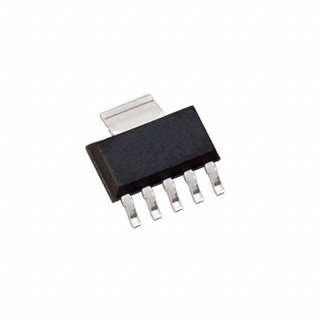
| 描述 | IC REG LDO ADJ 0.25A SOT223-6低压差稳压器 High PSRR Fast RF High-Enable 250-mA |
| 产品分类 | |
| 品牌 | Texas Instruments |
| 产品手册 | |
| 产品图片 |
|
| rohs | 符合RoHS无铅 / 符合限制有害物质指令(RoHS)规范要求 |
| 产品系列 | 电源管理 IC,低压差稳压器,Texas Instruments TPS79401DCQ- |
| 数据手册 | |
| 产品型号 | TPS79401DCQ |
| 产品种类 | 低压差稳压器 |
| 供应商器件封装 | SOT-223-6 |
| 其它名称 | TPS79401DCQG4 |
| 包装 | 管件 |
| 单位重量 | 121 mg |
| 参考电压 | 1.2246 V |
| 商标 | Texas Instruments |
| 安装类型 | 表面贴装 |
| 安装风格 | SMD/SMT |
| 封装 | Tube |
| 封装/外壳 | SOT-223-6 |
| 封装/箱体 | SOT-223-6 |
| 工作温度 | -40°C ~ 125°C |
| 工厂包装数量 | 78 |
| 最大工作温度 | + 125 C |
| 最大输入电压 | 5.5 V |
| 最小工作温度 | - 40 C |
| 最小输入电压 | + 2.7 V |
| 标准包装 | 78 |
| 电压-跌落(典型值) | 0.145V @ 250mA |
| 电压-输入 | 2.7 V ~ 5.5 V |
| 电压-输出 | 1.2 V ~ 5.5 V |
| 电压调节准确度 | 3 % |
| 电流-输出 | 250mA |
| 电流-限制(最小值) | - |
| 稳压器拓扑 | 正,可调式 |
| 稳压器数 | 1 |
| 系列 | TPS79401 |
| 线路调整率 | 0.05 % / V |
| 负载调节 | 10 mV |
| 输入偏压电流—最大 | 0.17 mA |
| 输出电压 | 1.2 V to 5.5 V |
| 输出电流 | 250 mA |
| 输出端数量 | 1 Output |
| 输出类型 | Adjustable |
| 配用 | /product-detail/zh/XILINXPWR-079/296-19048-ND/863869 |


- 商务部:美国ITC正式对集成电路等产品启动337调查
- 曝三星4nm工艺存在良率问题 高通将骁龙8 Gen1或转产台积电
- 太阳诱电将投资9.5亿元在常州建新厂生产MLCC 预计2023年完工
- 英特尔发布欧洲新工厂建设计划 深化IDM 2.0 战略
- 台积电先进制程称霸业界 有大客户加持明年业绩稳了
- 达到5530亿美元!SIA预计今年全球半导体销售额将创下新高
- 英特尔拟将自动驾驶子公司Mobileye上市 估值或超500亿美元
- 三星加码芯片和SET,合并消费电子和移动部门,撤换高东真等 CEO
- 三星电子宣布重大人事变动 还合并消费电子和移动部门
- 海关总署:前11个月进口集成电路产品价值2.52万亿元 增长14.8%


PDF Datasheet 数据手册内容提取
TPS794xx www.ti.com SLVS349E–NOVEMBER2001–REVISEDDECEMBER2005 ULTRALOW-NOISE, HIGH-PSRR, FAST, RF, 250-mA LOW-DROPOUT LINEAR REGULATORS FEATURES DESCRIPTION • 250-mALow-DropoutRegulatorWithEnable The TPS794xx family of low-dropout (LDO) linear • AvailableinFixedandAdjustable(1.2Vto voltage regulators features high power-supply 5.5V)Versions rejection ratio (PSRR), ultralow-noise, fast start-up, and excellent line and load transient responses in • HighPSRR(60dBat10kHz) small outline, MSOP-8 PowerPAD™ and SOT223-6 • UltralowNoise(32m Vrms,TPS79428) packages. Each device in the family is stable with a • FastStart-UpTime(50m s) small 2.2-m F ceramic capacitor on the output. The • StableWitha2.2-m FCeramicCapacitor family uses an advanced, proprietary BiCMOS fabrication process to yield extremely low dropout • ExcellentLoad/LineTransientResponse voltages (for example, 155 mV at 250mA). Each • VeryLowDropoutVoltage(155mVatFull device achieves fast start-up times (approximately Load) 50m s with a 0.001-m F bypass capacitor) while • AvailableinMSOP-8andSOT223-6Packages consuming low quiescent current (170 m A typical). Moreover, when the device is placed in standby mode, the supply current is reduced to less than APPLICATIONS 1 m A. The TPS79428 exhibits approximately • RF:VCOs,Receivers,ADCs 32 m V of output voltage noise at 2.8 V output with RMS • Audio a 0.1-m F bypass capacitor. Applications with analog • Bluetooth™,WirelessLAN components that are noise-sensitive, such as portable RF electronics, benefit from the high PSRR • CellularandCordlessTelephones and low noise features as well as the fast response • HandheldOrganizers,PDAs time. DGN PACKAGE MSOP-8 PowerPAD(cid:1) TPS79433 TPS79428 (TOP VIEW) RIPPLE REJECTION OUTPUT SPECTRAL NOISE DENSITY vs vs OUT 1 8 IN NC 2 7 NC FREQUENCY FREQUENCY GONUENINNFDNTCRB − DNCo( TQSi34nO2341O tPePTAr n2VCa2IEKl3 c-WA6o65Gn)nEect6GiGoENnNNDD Ripple Rejection (dB) 421679358000000000 VVCCCIOIONNNURU ==T T= 41== 0. 3m31.0 F.0V31, I, mOVmFU,F,T = 10 mIAOUT = 250 mA m√Output Spectral Noise Density (V/Hz) 0000000.......011223350505050 IOUTI O=U 2T5 =0CCV 1IONmN RUm A= T=A 3= 0. 8.21 .V 2m mF,F, 0 NR/FB 5 10 100 1 k 10 k 100 k 1 M 10 M 100 1000 10000 100000 Frequency (Hz) Frequency (Hz) Pleasebeawarethatanimportantnoticeconcerningavailability,standardwarranty,anduseincriticalapplicationsofTexas Instrumentssemiconductorproductsanddisclaimerstheretoappearsattheendofthisdatasheet. PowerPADisatrademarkofTexasInstruments. BluetoothisatrademarkofBluetoothSIG,Inc. Allothertrademarksarethepropertyoftheirrespectiveowners. PRODUCTIONDATAinformationiscurrentasofpublicationdate. Copyright©2001–2005,TexasInstrumentsIncorporated Products conform to specifications per the terms of the Texas Instruments standard warranty. Production processing does not necessarilyincludetestingofallparameters.
TPS794xx www.ti.com SLVS349E–NOVEMBER2001–REVISEDDECEMBER2005 This integrated circuit can be damaged by ESD. Texas Instruments recommends that all integrated circuits be handled with appropriateprecautions.Failuretoobserveproperhandlingandinstallationprocedurescancausedamage. ESD damage can range from subtle performance degradation to complete device failure. Precision integrated circuits may be more susceptible to damage because very small parametric changes could cause the device not to meet its published specifications. ORDERINGINFORMATION(1) PRODUCT VOUT(2) TPS794xxyyyz XXisnominaloutputvoltage(forexample,28=2.8V,285=2.85V,01=Adjustable). YYYispackagedesignator. Zispackagequantity. (1) Forthemostcurrentpackageandorderinginformation,seethePackageOptionAddendumattheendofthisdocument,orseetheTI websiteatwww.ti.com. (2) Outputvoltagesfrom1.3Vto5.0Vin100mVincrementsareavailable;minimumorderquantitiesmayapply.Contactfactoryfordetails andavailability. ABSOLUTE MAXIMUM RATINGS overoperatingtemperaturerangeunlessotherwisenoted(1) VALUE VINrange –0.3Vto6V VENrange –0.3VtoVIN+0.3V VOUTrange –0.3Vto6V Peakoutputcurrent Internallylimited ESDrating,HBM 2kV ESDrating,CDM 500V Continuoustotalpowerdissipation SeeDissipationRatingsTable Junctiontemperaturerange,TJ –40(cid:176)Cto+150(cid:176)C Storagetemperaturerange,Tstg –65(cid:176)Cto+150(cid:176)C (1) Stressesbeyondthoselistedunderabsolutemaximumratingsmaycausepermanentdamagetothedevice.Thesearestressratings only,andfunctionaloperationofthedeviceattheseoranyotherconditionsbeyondthoseindicatedunderrecommendedoperating conditionsisnotimplied.Exposuretoabsolute-maximum-ratedconditionsforextendedperiodsmayaffectdevicereliability. PACKAGE DISSIPATION RATINGS PACKAGE AIR(CFFLMO)W ((cid:176)RCq/JWC) ((cid:176)RCq/JWA) POWTEA£R2R5A(cid:176)CTING POWTAER=7R0A(cid:176)CTING POWTAER=8R5A(cid:176)CTING 0 8.47 55.09 2.27W 1.45W 1.18W DGN 150 8.21 49.97 2.50W 1.60W 1.30W 250 8.20 48.10 2.60W 1.66W 1.35W 6 5 4 Condition 1 CONDITIONS PACKAGE PCB AREA q JA W) (D 3 1 SOT223 4in2 Top Side Only 53°C/W P Condition 2 2 SOT223 0.5in2 Top Side Only 110°C/W 2 1 0 0 25 50 75 100 125 150 TA (°C) Figure1.SOT223PowerDissipation 2 SubmitDocumentationFeedback
TPS794xx www.ti.com SLVS349E–NOVEMBER2001–REVISEDDECEMBER2005 ELECTRICAL CHARACTERISTICS Overrecommendedoperatingtemperaturerange(T =–40(cid:176) Cto125(cid:176) C),V =V ,V =V +1V(1),I =1mA, J EN IN IN OUT(nom) OUT C =10m F,C =0.01m F,unlessotherwisenoted.Typicalvaluesareat25(cid:176) C. OUT NR PARAMETER TESTCONDITIONS MIN TYP MAX UNIT Inputvoltage,VIN(1) 2.7 5.5 V Continuousoutputcurrent,IOUT 0 250 mA Outputvoltagerange TPS79401 1.225 5.5–VDO V Ovoulttapguet Accuracy TPS79401(2) 0m A£ IOUT£ 250mA,VOUT+1V£ VIN£ 5.5V(1) 0.97(VOUT) VOUT 1.03(VOUT) V FixedVOUT 0m A£ IOUT£ 250mA,VOUT+1V£ VIN£ 5.5V(1) –3.0 +3.0 % Outputvoltagelineregulation(D VOUT%/D VIN)(1) VOUT+1V£ VIN£ 5.5V 0.05 0.12 %/V Loadregulation(D VOUT%/D IOUT) 0m A£ IOUT£ 250mA 10 mV TPS79428 IOUT=250mA 155 210 Dropoutvoltage(3) VIN=VOUT(nom)–0.1V TPS79430 IOUT=250mA 155 210 mV TPS79433 IOUT=250mA 145 200 Outputcurrentlimit VOUT=0V 925 mA Groundpincurrent 0m A£ IOUT£ 250mA 170 220 m A Shutdowncurrent(4) VEN=0V,2.7V£ VIN£ 5.5V 0.07 1 m A FBpincurrent VFB=1.225V 1 m A f=100Hz,IOUT=250mA 65 Power-supplyripplerejection TPS79428 f=10kHz,IOUT=250mA 60 dB f=100kHz,IOUT=250mA 40 CNR=0.001m F 55 Outputnoisevoltage TPS79428 BIOWUT==120500HmzAto100kHz, CCNNRR==00..00014m7Fm F 3363 m VRMS CNR=0.1m F 32 CNR=0.001m F 50 Time,start-up TPS79428 RL=14W ,COUT=1m F CNR=0.0047m F 70 m s CNR=0.01m F 100 High-levelenableinputvoltage 2.7V£ VIN£ 5.5V 1.7 VIN V Low-levelenableinputvoltage 2.7V£ VIN£ 5.5V 0 0.7 V ENpincurrent VEN=0 1 1 m A UVLOthreshold VCCrising 2.25 2.65 V UVLOhysteresis 100 mV (1) MinimumV is2.7VorV +V ,whicheverisgreater. IN OUT DO (2) Toleranceofexternalresistorsnotincludedinthisspecification. (3) DropoutisnotmeasuredfortheTPS79418andTPS79425sinceminimumV =2.7V. IN (4) Foradjustableversions,thisappliesonlyafterV isapplied;thenV transitionshightolow. IN EN SubmitDocumentationFeedback 3
TPS794xx www.ti.com SLVS349E–NOVEMBER2001–REVISEDDECEMBER2005 FUNCTIONALBLOCKDIAGRAM—ADJUSTABLEVERSION IN OUT UVLO Current Sense SHUTDOWN ILIM GND _ + R1 FB EN UVLO R2 Thermal Shutdown Quickstart External to the Device Bandgap Reference 250 kW Vref VIN 1.225 V NR(1) (1) Not Available on DCQ (SOT223) options. FUNCTIONALBLOCKDIAGRAM—FIXEDVERSION IN OUT UVLO Current Sense GND SHUTDOWN ILIM _ R1 + EN UVLO Thermal R2 Shutdown Quickstart R2 = 40k Bandgap VIN Reference 250 kW Vref NR 1.225 V TerminalFunctions TERMINAL DGN DCQ DESCRIPTION NAME (MSOP) (SOT223) Connectinganexternalcapacitortothispinbypassesnoisegeneratedbytheinternalbandgap,which NR 4 5 improvespower-supplyrejectionandreducesoutputnoise. TheENterminalisaninputthatenablesorshutsdownthedevice.WhenENisalogichigh,thedevice EN 6 1 isenabled.Whenthedeviceisalogiclow,thedeviceisinshutdownmode. FB 3 5 Feedbackinputvoltagefortheadjustabledevice. GND 5,PAD 3,6 Regulatorground IN 8 2 Unregulatedinputtothedevice. NC 2,7 Nointernalconnection. OUT 1 4 Regulatoroutput 4 SubmitDocumentationFeedback
TPS794xx www.ti.com SLVS349E–NOVEMBER2001–REVISEDDECEMBER2005 TYPICAL CHARACTERISTICS TPS79433 TPS79428 TPS79428 OUTPUTVOLTAGE OUTPUTVOLTAGE GROUNDCURRENT vsOUTPUTCURRENT vsJUNCTIONTEMPERATURE vsJUNCTIONTEMPERATURE 3.290 2.800 190 VIN = 3.8 V, 3.285 2.795 IOUT = 1 mA 185 COUT = 10 m F 3.280 180 2.790 IOUT = 1 mA (V) 3.275 (V) 2.785 VCIONU =T 3=. 81 0V m F A) 175 VOUT33..226750 VOUT2.780 mI (GND 116750 IOUT = 250 mA 3.260 2.775 160 3.255 2.770 IOUT = 200 mA 155 3.250 2.765 150 0 50 100 200 250 −40−25−105 20 35 50 65 80 95 110125 −40−25−10 5 20 35 50 65 80 95110125 IOUT (mA) TJ (°C) TJ (°C) Figure2. Figure3. Figure4. TPS79428 TPS79428 TPS79428 OUTPUTSPECTRAL OUTPUTSPECTRAL OUTPUTSPECTRAL NOISEDENSITY NOISEDENSITY NOISEDENSITY vsFREQUENCY vsFREQUENCY vsFREQUENCY m√Output Spectral Noise Density (V/Hz) 0000000.......01122335050505 IOUT =I O25U0T m=CCV A1IONN RUm = T=A 3= 0. 8.21 .V 2m mF,F, m√Output Spectral Noise Density (V/Hz) 0000000.......01122335050505 CCVIONNRU = T= 3= 0. 8.11 0VI O mImOUFFU,T,T = = 2 15 0m mAA m√Output Spectral Noise Density (V/Hz) 000011111.........246824608 CCCNNNRRR C= N= =0R 0.0 0.=CIV.00O0 IO0101UN4U . T 1mm=7T FF= m3m= F2.F 815 00V mmFA, 0 0 0 100 1000 10000 100000 100 1000 10000 100000 100 1000 10000 100000 Frequency (Hz) Frequency (Hz) Frequency (Hz) Figure5. Figure6. Figure7. TPS79428 TPS79433 TPS79428 ROOTMEANSQUARED OUTPUTIMPEDANCE DROPOUTVOLTAGE OUTPUTNOISEvsC vsFREQUENCY vsJUNCTIONTEMPERATURE NR 60 10 250 50 ICOOUUTT = = 2 1500 mmFA, VCIONU =T 4=. 31 0V ,m F, VCIONU =T 3=. 81 0V ,m F )S ) 200 mOutput Noise (VRM 234000 WOutput Impedance ( 1 IOUT = 1 mA V (mV)DO 110500 IOUT = 250 mA RMS 10 Z, O 0.100 IOUT = 250 mA 50 IOUT = 1 mA 0 0.020 0 0.001 0.0047 0.01 0.1 10 100 1 k 10 k 100 k 1 M 10 M −40−25−10 5 20 35 50 65 80 95110125 CNR (m F) Frequency (Hz) TJ (°C) Figure8. Figure9. Figure10. SubmitDocumentationFeedback 5
TPS794xx www.ti.com SLVS349E–NOVEMBER2001–REVISEDDECEMBER2005 TYPICAL CHARACTERISTICS (continued) TPS79433 TPS79433 TPS79433 RIPPLEREJECTION RIPPLEREJECTION RIPPLEREJECTION vsFREQUENCY vsFREQUENCY vsFREQUENCY 90 90 90 80 IOUT = 10 mA 80 IOUT = 10 mA 80 IOUT = 10 mA 70 70 70 Ripple Rejection (dB) 4263500000 VVCIOINNU ==T 41=. 3m3 F.V3,, V, IOUT = 250 mA Ripple Rejection (dB) 4263500000 VVCIOINNU ==T 41=. 3m3 F.V3,, V, IOUT = 250 mA Ripple Rejection (dB) 4263500000 VVCIOINNU ==T 41=. 3m3 F.V3,, V, IOUT = 250 mA 10 COUT = 10 m F, 10 COUT = 2.2 m F, 10 COUT = 2.2 m F, CNR = 0.01 m F CNR = 0.01 m F CNR = 0.1 m F 0 0 0 10 100 1 k 10 k 100 k 1 M 10 M 10 100 1 k 10 k 100 k 1 M 10 M 10 100 1 k 10 k 100 k 1 M 10 M Frequency (Hz) Frequency (Hz) Frequency (Hz) Figure11. Figure12. Figure13. TPS79433 OUTPUTVOLTAGE, TPS79433 TPS79433 ENABLEVOLTAGE LINETRANSIENT LOADTRANSIENT vsTIME(START-UP) RESPONSE RESPONSE 6.0 V_Enable IOUT = 250 mA,COUT = 10 m F, 24 VVIONU =T =4. 33 .V3 ,V, V (V)IN 55..05 CNR = 0.1 m F, dv/dt = 1 V/m s (mA)T 250 V) 0 ICOOUUTT = = 2 25.02 mmFA, 4.5 IOU 0 (N E V 10 , T VOU 312 CNR = C0N.0R0 =4 70 .m0F01 mF DV (mV)OUT −−21000 DV (mV)OUT −55000 VCIONU =T 4=. 31 0V ,m F ddit (cid:1) 0.(cid:1)0s2A 0 −30 0 80 160240320400480560640720800 0 100 200 300 400 500 0 30 60 90 120 150 180 210 Time (m s) Time (m s) Time (m s) Figure14. Figure15. Figure16. TPS79425 TPS79433 TPS79401 POWER-UP/ DROPOUTVOLTAGE DROPOUTVOLTAGE POWER-DOWN vsOUTPUTCURRENT vsINPUTVOLTAGE 4.5 200 250 34..50 VROL U=T 1 =0 2W.5 V, TA = 125°C 200 TA = 125°CTA = 25°C v) VIN 150 V/di 3.0 TA = 25°C 00 m 2.5 VOUT mV) mV) 150 ower-Up (5 112...050 V (DO 100 TA = −40°C V (DO 100 TA = −40°C P 50 0.5 50 COUT = 10 m F, CNR = 0.01 m F, 0 IOUT = 250 mA −0.5 0 0 0 1.4 2.8 4.2 5.6 7.0 8.4 9.8 0 25 50 75 100 125150175200 225250 2.5 3.0 3.5 4.0 4.5 5.0 t (ms) IOUT (mA) VIN (V) Figure17. Figure18. Figure19. 6 SubmitDocumentationFeedback
TPS794xx www.ti.com SLVS349E–NOVEMBER2001–REVISEDDECEMBER2005 TYPICAL CHARACTERISTICS (continued) TPS79428 TPS79428 TYPICALREGIONSOFSTABILITY TYPICALREGIONSOFSTABILITY EQUIVALENTSERIESRESISTANCE EQUIVALENTSERIESRESISTANCE (ESR) (ESR) vsOUTPUTCURRENT vsOUTPUTCURRENT 100 100 WResistance () 10 CTAO U= T− =4 02 .t2o m8F5R°eCgion of Instability WResistance () 10 CTAO U= T− =4 01 0to m 8FR5°eCgion of Instability Series 1 Series 1 Equivalent 0.1 Equivalent 0.1 R, Region of Stability R, Region of Stability S S E E 0.01 0.01 0 25 50 75 100125150175200225250 1 10 20 40 60 80 120 200 250 IOUT (mA) IOUT (mA) Figure20. Figure21. SubmitDocumentationFeedback 7
TPS794xx www.ti.com SLVS349E–NOVEMBER2001–REVISEDDECEMBER2005 APPLICATION INFORMATION order for the regulator to operate properly, the The TPS794xx family of low-dropout (LDO) current flow out of the NR pin must be at a minimum, regulators has been optimized for use in because any leakage current creates an IR drop noise-sensitive equipment. The device features across the internal resistor, thus creating an output extremely low dropout voltages, high PSRR, ultralow error. Therefore, the bypass capacitor must have output noise, low quiescent current (265 m A minimal leakage current. The bypass capacitor typically), and an enable input to reduce supply should be no more than 0.1-m F in order to ensure currents to less than that it is fully charged during the quickstart time 1m Awhentheregulatoristurnedoff. provided by the internal switch shown in the AtypicalapplicationcircuitisshowninFigure22. FunctionalBlockDiagram. For example, the TPS79430 exhibits only 33 m V RMS of output voltage noise using a 0.1-m F ceramic VIN IN OUT VOUT bypass capacitor and a 10-m F ceramic output TPS794xx capacitor. Note that the output starts up slower as 1 m F EN GND NR 2.2m F thebypasscapacitanceincreasesbecauseofthe RC 0.01m F time constant at the bypass pin that is created by the internal250-kW resistorandexternalcapacitor. BOARD LAYOUT RECOMMENDATION TO IMPROVE PSRR AND NOISE Figure22.TypicalApplicationCircuit PERFORMANCE To improve ac measurements such as PSRR, output EXTERNAL CAPACITOR REQUIREMENTS noise, and transient response, it is recommended A 1-m F or larger ceramic input bypass capacitor, that the board be designed with separate ground planes for V and V , with each ground plane connected between IN and GND and located close IN OUT connected only at the ground pin of the device. In to the TPS794xx, is required for stability and addition, the ground connection for the bypass improves transient response, noise rejection, and capacitor should connect directly to the ground pin of ripple rejection. A higher-value input capacitor may thedevice. be necessary if large, fast-rise-time load transients are anticipated and the device is located several inchesfromthepowersource. REGULATOR MOUNTING Like most low-dropout regulators, the TPS794xx The tab of the SOT223-6 package is electrically requires an output capacitor connected between connected to ground. For best thermal performance, OUT and GND to stabilize the internal control loop. the tab of the surface-mount version should be The minimum recommended capacitance is 1 m F. soldered directly to a circuit-board copper area. Any Increasing the copper area improves heat 1m Forlargerceramiccapacitorissuitable. dissipation. The internal voltage reference is a key source of Solder pad footprint recommendations for the noise in an LDO regulator. The TPS794xx has an devices are presented in Application Report NR pin which is connected to the voltage reference SBFA015, Solder Pad Recommendations for through a 250-kW internal resistor. The 250-kW Surface-Mount Devices, available from the TI web internal resistor, in conjunction with an external site(www.ti.com). bypass capacitor connected to the NR pin, creates a low-pass filter to reduce the voltage reference noise and, therefore, the noise at the regulator output. In 8 SubmitDocumentationFeedback
TPS794xx www.ti.com SLVS349E–NOVEMBER2001–REVISEDDECEMBER2005 PROGRAMMING THE TPS79401 In order to improve the stability of the adjustable ADJUSTABLE LDO REGULATOR version, it is suggested that a small compensation capacitorbeplacedbetweenOUTandFB. The output voltage of the TPS79401 adjustable regulator is programmed using an external resistor The approximate value of this capacitor can be divider as shown in Figure 23. The output voltage is calculatedasEquation3: calculatedusingEquation1: (3(cid:1)10(cid:3)7)(cid:1)(R (cid:2)R ) (cid:4) (cid:5) C (cid:4) 1 2 V (cid:3)V (cid:1) 1(cid:2)R1 1 (R1(cid:1)R2) (3) OUT REF R 2 (1) The suggested value of this capacitor for several resistor ratios is shown in the table within Figure 23. where: If this capacitor is not used (such as in a unity-gain • V = 1.2246 V typ (the internal reference REF configuration), then the minimum recommended voltage) outputcapacitoris2.2m Finsteadof1m F. Resistors R and R should be chosen for 1 2 approximately 40-m A divider current. Lower value REGULATOR PROTECTION resistors can be used for improved noise The TPS794xx PMOS-pass transistor has a built-in performance, but the device wastes more power. back diode that conducts reverse current when the Higher values should be avoided, as leakage current input voltage drops below the output voltage (for atFBincreasestheoutputvoltageerror. example, during power down). Current is conducted The recommended design procedure is to choose from the output to the input and is not internally R = 30.1kW to set the divider current at 40 m A, limited. If extended reverse voltage operation is 2 C = 15 pF for stability, and then calculate R using anticipated,externallimitingmightbeappropriate. 1 1 Equation2: (cid:4) (cid:5) The TPS794xx features internal current limiting and V thermal protection. During normal operation, the R (cid:3) OUT(cid:2)1 (cid:1)R 1 V 2 TPS794xx limits output current to approximately REF (2) 2.8 A. When current limiting engages, the output voltage scales back linearly until the overcurrent condition ends. While current limiting is designed to prevent gross device failure, care should be taken not to exceed the power dissipation ratings of the package. If the temperature of the device exceeds approximately 165(cid:176) C, thermal-protection circuitry shuts it down. Once the device has cooled down to below approximately 140(cid:176) C, regulator operation resumes. OUTPUT VOLTAGE PROGRAMMING GUIDE VIN IN OUT VOUT OUTPUT 1m F EN TPS79401 R1 C1 2.2m F VOLTAGE R1 R2 C1 GND FB 1.8 V 14.0 kW 30.1 kW 22 pF R2 3.6 V 61.9 kW 30.1 kW 15 pF Figure23.TPS79401AdjustableLDORegulatorProgramming SubmitDocumentationFeedback 9
TPS794xx www.ti.com SLVS349E–NOVEMBER2001–REVISEDDECEMBER2005 THERMAL INFORMATION The amount of heat that an LDO linear regulator generates is directly proportional to the amount of A TJ power it dissipates during operation. All integrated circuits have a maximum allowable junction CIRCUIT BOARD COPPER AREA Rq JC temperature (T max) above which normal operation J C is not assured. A system designer must design the B TC B operating environment so that the operating junction temperature (T ) does not exceed the maximum Rq CS J junction temperature (T max). The two main A J environmental variables that a designer can use to C improve thermal performance are air flow and external heatsinks. The purpose of this information is Rq SA to aid the designer in determining the proper operating environment for a linear regulator that is SOT223 Package operatingataspecificpowerlevel. TA In general, the maximum expected power (P max) D consumed by a linear regulator is computed as Figure24.ThermalResistances showninEquation4: (cid:5) (cid:6) P max(cid:4) V (cid:3)V (cid:1)I (cid:2) V (cid:1)I Equation5summarizesthecomputation: D IN(avg) OUT(avg) OUT(avg) I(avg) Q T (cid:3) T (cid:2)P max (cid:1) (cid:4)R (cid:2) R (cid:2) R (cid:5) (4) J A D q JC q CS q SA (5) where: The R is specific to each regulator as determined Q JC • V istheaverageinputvoltage by its package, lead frame, and die size provided in IN(avg) • V istheaverageoutputvoltage the regulator's data sheet. The RQ SA is a function of OUT(avg) the type and size of heatsink. For example, black • I istheaverageoutputcurrent • IOQUiTs(atvhge) quiescentcurrent braondgyinrgadifarotomr ty5p(cid:176) Ce/WheaftosirnkvsercyanlahrgaevehReQaCtsSinvkasluetos 50(cid:176) C/W for very small heatsinks. The R is a For most TI LDO regulators, the quiescent current is Q CS function of how the package is attached to the insignificant compared to the average output current; heatsink. For example, if a thermal compound is therefore,thetermV xI canbe neglected. The IN(avg) Q used to attach a heatsink to a SOT223 package, operating junction temperature is computed by R of1(cid:176) C/Wisreasonable. adding the ambient temperature (T ) and the Q CS A increase in temperature due to the regulator's power Even if no external black body radiator type heatsink dissipation. The temperature rise is computed by is attached to the package, the board on which the multiplying the maximum expected power dissipation regulator is mounted provides some heatsinking by the sum of the thermal resistances between the through the pin solder connections. Some packages, junction and the case (RQ JC), the case to heatsink like the DDPAK and SOT223 packages, use a (RQ CS), and the heatsink to ambient (RQ SA). Thermal copper plane underneath the package or the circuit resistances are measures of how effectively an board ground plane for additional heatsinking to object dissipates heat. Typically, the larger the improve their thermal performance. Computer-aided device, the more surface area available for power thermal modeling can be used to compute very dissipation and the lower the object's thermal accurate approximations of an integrated circuit's resistance. thermal performance in different operating environments (for example, different types of circuit Figure 24 illustrates these thermal resistances for a boards, different types and sizes of heatsinks, SOT223packagemountedinaJEDEClow-Kboard. different air flows, etc.). Using these models, the three thermal resistances can be combined into one thermal resistance between junction and ambient (R ). This R is valid only for the specific Q JA Q JA operatingenvironmentusedinthecomputermodel. 10 SubmitDocumentationFeedback
TPS794xx www.ti.com SLVS349E–NOVEMBER2001–REVISEDDECEMBER2005 Equation5simplifiesintoEquation6: applications. The SOT223 package dimensions are T (cid:3) T (cid:2)P max (cid:1) R provided in the Mechanical Data section at the end J A D q JA (6) of the data sheet. The addition of a copper plane RearrangingEquation6givesEquation7: directly underneath the SOT223 package enhances T (cid:1)T thethermalperformanceofthepackage. R (cid:2) J A q JA PDmax (7) To illustrate, the TPS79425 in a SOT223 package was chosen. For this example, the average input Using Equation 6 and the computer model generated voltage is 3.3 V, the output voltage is 2.5 V, the curves shown in Figure 25, a designer can quickly average output current is 1 A, the ambient compute the required heatsink thermal temperature 55(cid:176) C, no air flow is present, and the resistance/board area for a given ambient operating environment is the same as documented temperature, power dissipation, and operating below. Neglecting the quiescent current, the environment. maximumaveragepowerisEquation8: P max (cid:3) (3.3 (cid:2) 2.5)V (cid:1) 1A (cid:3) 800mW D (8) 180 W) 160 No Air Flow SEuqbusattiitountin9g: TJmax for TJ into Equation 4 gives C/ °e ( 140 Rq JAmax (cid:2) (125 (cid:1) 55)°C(cid:3)800mW (cid:2) 87.5°C(cid:3)W nc 120 (9) a sist 100 From Figure 25, Rq JA vs PCB Copper Area, the Re ground plane needs to be 0.55 in2 for the part to al 80 dissipate 800 mW. The operating environment used m er 60 toconstructFigure25consisted of a board with 1 oz. h T copper planes. The package is soldered to a 1 oz. − A 40 copper pad on the top of the board. The pad is tied RqJ 20 throughthermalviastothe1oz.groundplane. 0 From the data in Figure 25 and rearranging equation 0.1 1 10 6, the maximum power dissipation for a different PCB Copper Area (in2) ground plane area and a specific ambient temperature can be computed, as shown in Figure26. Figure25.SOT223ThermalResistancevsPCB CopperArea 6 SOT223 POWER DISSIPATION n (W) 5 TA = 25°C o The SOT223 package provides an effective means ati p of managing power dissipation in surface-mount si 4 Dis 4 in2 PCB Area er w 3 o P 0.5 in2 PCB Area m u 2 m xi a M 1 − D P 0 0 25 50 75 100 125 150 TA − Ambient Temperature (°C) Figure26.SOT223MaximumPowerDissipation vsAmbientTemperature SubmitDocumentationFeedback 11
PACKAGE OPTION ADDENDUM www.ti.com 6-Feb-2020 PACKAGING INFORMATION Orderable Device Status Package Type Package Pins Package Eco Plan Lead/Ball Finish MSL Peak Temp Op Temp (°C) Device Marking Samples (1) Drawing Qty (2) (6) (3) (4/5) TPS79401DCQ ACTIVE SOT-223 DCQ 6 78 Green (RoHS NIPDAU Level-2-260C-1 YEAR -40 to 85 PS79401 & no Sb/Br) TPS79401DCQR ACTIVE SOT-223 DCQ 6 2500 Green (RoHS NIPDAU Level-2-260C-1 YEAR -40 to 85 PS79401 & no Sb/Br) TPS79401DCQRG4 ACTIVE SOT-223 DCQ 6 2500 Green (RoHS NIPDAU Level-2-260C-1 YEAR -40 to 85 PS79401 & no Sb/Br) TPS79401DGNR ACTIVE HVSSOP DGN 8 2500 Green (RoHS NIPDAU | NIPDAUAG Level-1-260C-UNLIM -40 to 85 AXL & no Sb/Br) TPS79401DGNRG4 ACTIVE HVSSOP DGN 8 2500 Green (RoHS NIPDAUAG Level-1-260C-UNLIM -40 to 85 AXL & no Sb/Br) TPS79401DGNT ACTIVE HVSSOP DGN 8 250 Green (RoHS NIPDAU | NIPDAUAG Level-1-260C-UNLIM -40 to 85 AXL & no Sb/Br) TPS79418DCQ ACTIVE SOT-223 DCQ 6 78 Green (RoHS NIPDAU Level-2-260C-1 YEAR -40 to 85 PS79418 & no Sb/Br) TPS79418DCQR ACTIVE SOT-223 DCQ 6 2500 Green (RoHS NIPDAU Level-2-260C-1 YEAR -40 to 85 PS79418 & no Sb/Br) TPS79418DGNR ACTIVE HVSSOP DGN 8 2500 Green (RoHS NIPDAU Level-1-260C-UNLIM -40 to 85 AXM & no Sb/Br) TPS79418DGNT ACTIVE HVSSOP DGN 8 250 Green (RoHS NIPDAU Level-1-260C-UNLIM -40 to 85 AXM & no Sb/Br) TPS79418DGNTG4 ACTIVE HVSSOP DGN 8 250 Green (RoHS NIPDAU Level-1-260C-UNLIM -40 to 85 AXM & no Sb/Br) TPS79425DCQ ACTIVE SOT-223 DCQ 6 78 Green (RoHS NIPDAU Level-2-260C-1 YEAR -40 to 85 PS79425 & no Sb/Br) TPS79425DCQR ACTIVE SOT-223 DCQ 6 2500 Green (RoHS NIPDAU Level-2-260C-1 YEAR -40 to 85 PS79425 & no Sb/Br) TPS79425DGNR ACTIVE HVSSOP DGN 8 2500 Green (RoHS NIPDAU Level-1-260C-UNLIM -40 to 85 AYB & no Sb/Br) TPS79425DGNT ACTIVE HVSSOP DGN 8 250 Green (RoHS NIPDAU Level-1-260C-UNLIM -40 to 85 AYB & no Sb/Br) TPS79428DCQ ACTIVE SOT-223 DCQ 6 78 Green (RoHS NIPDAU Level-2-260C-1 YEAR -40 to 85 PS79428 & no Sb/Br) TPS79428DCQR ACTIVE SOT-223 DCQ 6 2500 Green (RoHS NIPDAU Level-2-260C-1 YEAR -40 to 85 PS79428 & no Sb/Br) Addendum-Page 1
PACKAGE OPTION ADDENDUM www.ti.com 6-Feb-2020 Orderable Device Status Package Type Package Pins Package Eco Plan Lead/Ball Finish MSL Peak Temp Op Temp (°C) Device Marking Samples (1) Drawing Qty (2) (6) (3) (4/5) TPS79428DGNT ACTIVE HVSSOP DGN 8 250 Green (RoHS NIPDAU Level-1-260C-UNLIM -40 to 85 AYC & no Sb/Br) TPS79430DCQ ACTIVE SOT-223 DCQ 6 78 Green (RoHS NIPDAU Level-2-260C-1 YEAR -40 to 85 PS79430 & no Sb/Br) TPS79430DCQG4 ACTIVE SOT-223 DCQ 6 78 Green (RoHS NIPDAU Level-2-260C-1 YEAR -40 to 85 PS79430 & no Sb/Br) TPS79430DCQR ACTIVE SOT-223 DCQ 6 2500 Green (RoHS NIPDAU Level-2-260C-1 YEAR -40 to 85 PS79430 & no Sb/Br) TPS79430DGNR ACTIVE HVSSOP DGN 8 2500 Green (RoHS NIPDAU Level-1-260C-UNLIM -40 to 85 AYD & no Sb/Br) TPS79430DGNT ACTIVE HVSSOP DGN 8 250 Green (RoHS NIPDAU Level-1-260C-UNLIM -40 to 85 AYD & no Sb/Br) TPS79433DCQ ACTIVE SOT-223 DCQ 6 78 Green (RoHS NIPDAU Level-2-260C-1 YEAR -40 to 85 PS79433 & no Sb/Br) TPS79433DCQR ACTIVE SOT-223 DCQ 6 2500 Green (RoHS NIPDAU Level-2-260C-1 YEAR -40 to 85 PS79433 & no Sb/Br) TPS79433DGNR ACTIVE HVSSOP DGN 8 2500 Green (RoHS NIPDAU Level-1-260C-UNLIM -40 to 85 AYE & no Sb/Br) TPS79433DGNRG4 ACTIVE HVSSOP DGN 8 2500 Green (RoHS NIPDAU Level-1-260C-UNLIM -40 to 85 AYE & no Sb/Br) TPS79433DGNT ACTIVE HVSSOP DGN 8 250 Green (RoHS NIPDAU Level-1-260C-UNLIM -40 to 85 AYE & no Sb/Br) (1) The marketing status values are defined as follows: ACTIVE: Product device recommended for new designs. LIFEBUY: TI has announced that the device will be discontinued, and a lifetime-buy period is in effect. NRND: Not recommended for new designs. Device is in production to support existing customers, but TI does not recommend using this part in a new design. PREVIEW: Device has been announced but is not in production. Samples may or may not be available. OBSOLETE: TI has discontinued the production of the device. (2) RoHS: TI defines "RoHS" to mean semiconductor products that are compliant with the current EU RoHS requirements for all 10 RoHS substances, including the requirement that RoHS substance do not exceed 0.1% by weight in homogeneous materials. Where designed to be soldered at high temperatures, "RoHS" products are suitable for use in specified lead-free processes. TI may reference these types of products as "Pb-Free". RoHS Exempt: TI defines "RoHS Exempt" to mean products that contain lead but are compliant with EU RoHS pursuant to a specific EU RoHS exemption. Green: TI defines "Green" to mean the content of Chlorine (Cl) and Bromine (Br) based flame retardants meet JS709B low halogen requirements of <=1000ppm threshold. Antimony trioxide based flame retardants must also meet the <=1000ppm threshold requirement. (3) MSL, Peak Temp. - The Moisture Sensitivity Level rating according to the JEDEC industry standard classifications, and peak solder temperature. Addendum-Page 2
PACKAGE OPTION ADDENDUM www.ti.com 6-Feb-2020 (4) There may be additional marking, which relates to the logo, the lot trace code information, or the environmental category on the device. (5) Multiple Device Markings will be inside parentheses. Only one Device Marking contained in parentheses and separated by a "~" will appear on a device. If a line is indented then it is a continuation of the previous line and the two combined represent the entire Device Marking for that device. (6) Lead/Ball Finish - Orderable Devices may have multiple material finish options. Finish options are separated by a vertical ruled line. Lead/Ball Finish values may wrap to two lines if the finish value exceeds the maximum column width. Important Information and Disclaimer:The information provided on this page represents TI's knowledge and belief as of the date that it is provided. TI bases its knowledge and belief on information provided by third parties, and makes no representation or warranty as to the accuracy of such information. Efforts are underway to better integrate information from third parties. TI has taken and continues to take reasonable steps to provide representative and accurate information but may not have conducted destructive testing or chemical analysis on incoming materials and chemicals. TI and TI suppliers consider certain information to be proprietary, and thus CAS numbers and other limited information may not be available for release. In no event shall TI's liability arising out of such information exceed the total purchase price of the TI part(s) at issue in this document sold by TI to Customer on an annual basis. Addendum-Page 3
PACKAGE MATERIALS INFORMATION www.ti.com 6-Sep-2019 TAPE AND REEL INFORMATION *Alldimensionsarenominal Device Package Package Pins SPQ Reel Reel A0 B0 K0 P1 W Pin1 Type Drawing Diameter Width (mm) (mm) (mm) (mm) (mm) Quadrant (mm) W1(mm) TPS79401DCQR SOT-223 DCQ 6 2500 330.0 12.4 7.1 7.45 1.88 8.0 12.0 Q3 TPS79401DGNR HVSSOP DGN 8 2500 330.0 12.4 5.3 3.4 1.4 8.0 12.0 Q1 TPS79401DGNT HVSSOP DGN 8 250 180.0 12.4 5.3 3.4 1.4 8.0 12.0 Q1 TPS79418DCQR SOT-223 DCQ 6 2500 330.0 12.4 7.1 7.45 1.88 8.0 12.0 Q3 TPS79418DGNR HVSSOP DGN 8 2500 330.0 12.4 5.3 3.4 1.4 8.0 12.0 Q1 TPS79418DGNT HVSSOP DGN 8 250 180.0 12.4 5.3 3.4 1.4 8.0 12.0 Q1 TPS79425DCQR SOT-223 DCQ 6 2500 330.0 12.4 7.1 7.45 1.88 8.0 12.0 Q3 TPS79425DGNR HVSSOP DGN 8 2500 330.0 12.4 5.3 3.4 1.4 8.0 12.0 Q1 TPS79425DGNT HVSSOP DGN 8 250 180.0 12.4 5.3 3.4 1.4 8.0 12.0 Q1 TPS79428DCQR SOT-223 DCQ 6 2500 330.0 12.4 7.1 7.45 1.88 8.0 12.0 Q3 TPS79428DGNT HVSSOP DGN 8 250 180.0 12.4 5.3 3.4 1.4 8.0 12.0 Q1 TPS79430DCQR SOT-223 DCQ 6 2500 330.0 12.4 7.1 7.45 1.88 8.0 12.0 Q3 TPS79430DGNR HVSSOP DGN 8 2500 330.0 12.4 5.3 3.4 1.4 8.0 12.0 Q1 TPS79430DGNT HVSSOP DGN 8 250 180.0 12.4 5.3 3.4 1.4 8.0 12.0 Q1 TPS79433DCQR SOT-223 DCQ 6 2500 330.0 12.4 7.1 7.45 1.88 8.0 12.0 Q3 TPS79433DGNR HVSSOP DGN 8 2500 330.0 12.4 5.3 3.4 1.4 8.0 12.0 Q1 TPS79433DGNT HVSSOP DGN 8 250 180.0 12.4 5.3 3.4 1.4 8.0 12.0 Q1 PackMaterials-Page1
PACKAGE MATERIALS INFORMATION www.ti.com 6-Sep-2019 *Alldimensionsarenominal Device PackageType PackageDrawing Pins SPQ Length(mm) Width(mm) Height(mm) TPS79401DCQR SOT-223 DCQ 6 2500 346.0 346.0 29.0 TPS79401DGNR HVSSOP DGN 8 2500 367.0 367.0 35.0 TPS79401DGNT HVSSOP DGN 8 250 210.0 185.0 35.0 TPS79418DCQR SOT-223 DCQ 6 2500 346.0 346.0 41.0 TPS79418DGNR HVSSOP DGN 8 2500 367.0 367.0 35.0 TPS79418DGNT HVSSOP DGN 8 250 210.0 185.0 35.0 TPS79425DCQR SOT-223 DCQ 6 2500 346.0 346.0 41.0 TPS79425DGNR HVSSOP DGN 8 2500 367.0 367.0 35.0 TPS79425DGNT HVSSOP DGN 8 250 210.0 185.0 35.0 TPS79428DCQR SOT-223 DCQ 6 2500 358.0 335.0 35.0 TPS79428DGNT HVSSOP DGN 8 250 210.0 185.0 35.0 TPS79430DCQR SOT-223 DCQ 6 2500 346.0 346.0 29.0 TPS79430DGNR HVSSOP DGN 8 2500 367.0 367.0 35.0 TPS79430DGNT HVSSOP DGN 8 250 210.0 185.0 35.0 TPS79433DCQR SOT-223 DCQ 6 2500 346.0 346.0 29.0 TPS79433DGNR HVSSOP DGN 8 2500 367.0 367.0 35.0 TPS79433DGNT HVSSOP DGN 8 250 210.0 185.0 35.0 PackMaterials-Page2
None
PACKAGE OUTLINE DGN0008D PowerPAD TM VSSOP - 1.1 mm max height SCALE 4.000 SMALL OUTLINE PACKAGE C 5.05 A 4.75 TYP 0.1 C PIN 1 INDEX AREA SEATING PLANE 6X 0.65 8 1 2X 3.1 1.95 2.9 NOTE 3 4 5 0.38 8X 0.25 B 3.1 0.13 C A B 2.9 NOTE 4 0.23 0.13 SEE DETAIL A EXPOSED THERMAL PAD 4 5 0.25 GAGE PLANE 1.89 1.63 9 1.1 MAX 8 1 0.7 0.15 0 -8 0.05 0.4 DETA 20AIL A 1.57 TYPICAL 1.28 4225481/A 11/2019 PowerPAD is a trademark of Texas Instruments. NOTES: 1. All linear dimensions are in millimeters. Any dimensions in parenthesis are for reference only. Dimensioning and tolerancing per ASME Y14.5M. 2. This drawing is subject to change without notice. 3. This dimension does not include mold flash, protrusions, or gate burrs. Mold flash, protrusions, or gate burrs shall not exceed 0.15 mm per side. 4. This dimension does not include interlead flash. Interlead flash shall not exceed 0.25 mm per side. 5. Reference JEDEC registration MO-187. www.ti.com
EXAMPLE BOARD LAYOUT DGN0008D PowerPAD TM VSSOP - 1.1 mm max height SMALL OUTLINE PACKAGE (2) NOTE 9 METAL COVERED BY SOLDER MASK (1.57) SYMM SOLDER MASK DEFINED PAD 8X (1.4) (R0.05) TYP 8 8X (0.45) 1 (3) 9 SYMM NOTE 9 (1.89) 6X (0.65) (1.22) 5 4 ( 0.2) TYP VIA (0.55) SEE DETAILS (4.4) LAND PATTERN EXAMPLE EXPOSED METAL SHOWN SCALE: 15X SOLDER MASK METAL METAL UNDER SOLDER MASK OPENING SOLDER MASK OPENING EXPOSED METAL EXPOSED METAL 0.05 MAX 0.05 MIN ALL AROUND ALL AROUND NON-SOLDER MASK SOLDER MASK DEFINED DEFINED (PREFERRED) SOLDE15.000R MASK DETAILS 4225481/A 11/2019 NOTES: (continued) 6. Publication IPC-7351 may have alternate designs. 7. Solder mask tolerances between and around signal pads can vary based on board fabrication site. 8. Vias are optional depending on application, refer to device data sheet. If any vias are implemented, refer to their locations shown on this view. It is recommended that vias under paste be filled, plugged or tented. 9. Size of metal pad may vary due to creepage requirement. www.ti.com
EXAMPLE STENCIL DESIGN DGN0008D PowerPAD TM VSSOP - 1.1 mm max height SMALL OUTLINE PACKAGE (1.57) BASED ON 0.125 THICK STENCIL SYMM 8X (1.4) (R0.05) TYP 8 8X (0.45) 1 (1.89) SYMM BASED ON 0.125 THICK STENCIL 6X (0.65) 4 5 METAL COVERED SEE TABLE FOR BY SOLDER MASK DIFFERENT OPENINGS (4.4) FOR OTHER STENCIL THICKNESSES SOLDER PASTE EXAMPLE EXPOSED PAD 9: 100% PRINTED SOLDER COVERAGE BY AREA SCALE: 15X STENCIL SOLDER STENCIL THICKNESS OPENING 0.1 1.76 X 2.11 0.125 1.57 X 1.89 (SHOWN) 0.15 1.43 X 1.73 0.175 1.33 X 1.60 4225481/A 11/2019 NOTES: (continued) 10. Laser cutting apertures with trapezoidal walls and rounded corners may offer better paste release. IPC-7525 may have alternate design recommendations. 11. Board assembly site may have different recommendations for stencil design. www.ti.com
PACKAGE OUTLINE DGN0008G PowerPAD TM VSSOP - 1.1 mm max height SCALE 4.000 SMALL OUTLINE PACKAGE C 5.05 A 4.75 TYP 0.1 C PIN 1 INDEX AREA SEATING PLANE 6X 0.65 8 1 2X 3.1 1.95 2.9 NOTE 3 4 5 0.38 8X 0.25 B 3.1 0.13 C A B 2.9 NOTE 4 0.23 0.13 SEE DETAIL A EXPOSED THERMAL PAD 4 5 0.25 GAGE PLANE 2.15 1.95 9 1.1 MAX 8 1 0.7 0.15 0 -8 0.05 0.4 DETA 20AIL A 1.846 TYPICAL 1.646 4225480/A 11/2019 PowerPAD is a trademark of Texas Instruments. NOTES: 1. All linear dimensions are in millimeters. Any dimensions in parenthesis are for reference only. Dimensioning and tolerancing per ASME Y14.5M. 2. This drawing is subject to change without notice. 3. This dimension does not include mold flash, protrusions, or gate burrs. Mold flash, protrusions, or gate burrs shall not exceed 0.15 mm per side. 4. This dimension does not include interlead flash. Interlead flash shall not exceed 0.25 mm per side. 5. Reference JEDEC registration MO-187. www.ti.com
EXAMPLE BOARD LAYOUT DGN0008G PowerPAD TM VSSOP - 1.1 mm max height SMALL OUTLINE PACKAGE (2) NOTE 9 METAL COVERED BY SOLDER MASK (1.846) SYMM SOLDER MASK DEFINED PAD 8X (1.4) (R0.05) TYP 8 8X (0.45) 1 (3) 9 SYMM NOTE 9 (2.15) 6X (0.65) (1.22) 5 4 ( 0.2) TYP VIA (0.55) SEE DETAILS (4.4) LAND PATTERN EXAMPLE EXPOSED METAL SHOWN SCALE: 15X SOLDER MASK METAL METAL UNDER SOLDER MASK OPENING SOLDER MASK OPENING EXPOSED METAL EXPOSED METAL 0.05 MAX 0.05 MIN ALL AROUND ALL AROUND NON-SOLDER MASK SOLDER MASK DEFINED DEFINED (PREFERRED) SOLDE15.000R MASK DETAILS 4225480/A 11/2019 NOTES: (continued) 6. Publication IPC-7351 may have alternate designs. 7. Solder mask tolerances between and around signal pads can vary based on board fabrication site. 8. Vias are optional depending on application, refer to device data sheet. If any vias are implemented, refer to their locations shown on this view. It is recommended that vias under paste be filled, plugged or tented. 9. Size of metal pad may vary due to creepage requirement. www.ti.com
EXAMPLE STENCIL DESIGN DGN0008G PowerPAD TM VSSOP - 1.1 mm max height SMALL OUTLINE PACKAGE (1.846) BASED ON 0.125 THICK STENCIL SYMM 8X (1.4) (R0.05) TYP 8 8X (0.45) 1 (2.15) SYMM BASED ON 0.125 THICK STENCIL 6X (0.65) 4 5 METAL COVERED SEE TABLE FOR BY SOLDER MASK DIFFERENT OPENINGS (4.4) FOR OTHER STENCIL THICKNESSES SOLDER PASTE EXAMPLE EXPOSED PAD 9: 100% PRINTED SOLDER COVERAGE BY AREA SCALE: 15X STENCIL SOLDER STENCIL THICKNESS OPENING 0.1 2.06 X 2.40 0.125 1.846 X 2.15 (SHOWN) 0.15 1.69 X 1.96 0.175 1.56 X 1.82 4225480/A 11/2019 NOTES: (continued) 10. Laser cutting apertures with trapezoidal walls and rounded corners may offer better paste release. IPC-7525 may have alternate design recommendations. 11. Board assembly site may have different recommendations for stencil design. www.ti.com
None
None
IMPORTANTNOTICEANDDISCLAIMER TI PROVIDES TECHNICAL AND RELIABILITY DATA (INCLUDING DATASHEETS), DESIGN RESOURCES (INCLUDING REFERENCE DESIGNS), APPLICATION OR OTHER DESIGN ADVICE, WEB TOOLS, SAFETY INFORMATION, AND OTHER RESOURCES “AS IS” AND WITH ALL FAULTS, AND DISCLAIMS ALL WARRANTIES, EXPRESS AND IMPLIED, INCLUDING WITHOUT LIMITATION ANY IMPLIED WARRANTIES OF MERCHANTABILITY, FITNESS FOR A PARTICULAR PURPOSE OR NON-INFRINGEMENT OF THIRD PARTY INTELLECTUAL PROPERTY RIGHTS. These resources are intended for skilled developers designing with TI products. You are solely responsible for (1) selecting the appropriate TI products for your application, (2) designing, validating and testing your application, and (3) ensuring your application meets applicable standards, and any other safety, security, or other requirements. These resources are subject to change without notice. TI grants you permission to use these resources only for development of an application that uses the TI products described in the resource. Other reproduction and display of these resources is prohibited. No license is granted to any other TI intellectual property right or to any third party intellectual property right. TI disclaims responsibility for, and you will fully indemnify TI and its representatives against, any claims, damages, costs, losses, and liabilities arising out of your use of these resources. TI’s products are provided subject to TI’s Terms of Sale (www.ti.com/legal/termsofsale.html) or other applicable terms available either on ti.com or provided in conjunction with such TI products. TI’s provision of these resources does not expand or otherwise alter TI’s applicable warranties or warranty disclaimers for TI products. Mailing Address: Texas Instruments, Post Office Box 655303, Dallas, Texas 75265 Copyright © 2020, Texas Instruments Incorporated