ICGOO在线商城 > 集成电路(IC) > PMIC - 稳压器 - 线性 > TPS76850QPWPREP
 Datasheet下载
- 型号: TPS76850QPWPREP
- 制造商: Texas Instruments
- 库位|库存: xxxx|xxxx
- 要求:
| 数量阶梯 | 香港交货 | 国内含税 |
| +xxxx | $xxxx | ¥xxxx |
查看当月历史价格
查看今年历史价格
TPS76850QPWPREP产品简介:
ICGOO电子元器件商城为您提供TPS76850QPWPREP由Texas Instruments设计生产,在icgoo商城现货销售,并且可以通过原厂、代理商等渠道进行代购。 TPS76850QPWPREP价格参考¥18.85-¥38.44。Texas InstrumentsTPS76850QPWPREP封装/规格:PMIC - 稳压器 - 线性, Linear Voltage Regulator IC Positive Fixed 1 Output 5V 1A 20-HTSSOP。您可以下载TPS76850QPWPREP参考资料、Datasheet数据手册功能说明书,资料中有TPS76850QPWPREP 详细功能的应用电路图电压和使用方法及教程。
TPS76850QPWPREP 是由 Texas Instruments(德州仪器)生产的一款 PMIC(电源管理集成电路),属于线性稳压器类别。该型号具有低功耗、高精度和小封装的特点,适用于多种电子设备和应用场景。以下是其主要应用场景:

1. 便携式电子设备
   TPS76850QPWPREP 的低功耗特性使其非常适合用于电池供电的便携式设备,例如智能手机、平板电脑、可穿戴设备(如智能手表和健康监测器)以及手持式医疗设备。它能够高效地将输入电压转换为稳定的输出电压,延长电池使用寿命。

2. 嵌入式系统
   在工业自动化、物联网(IoT)设备和其他嵌入式系统中,这款线性稳压器可用于为微控制器、传感器和通信模块提供稳定的电源。其小型封装设计便于集成到空间受限的设计中。

3. 通信设备
   该器件适合用于无线通信模块、蓝牙设备和 Zigbee 网络节点等场景。它能为射频(RF)电路和数字信号处理单元提供干净且稳定的电源,减少噪声干扰。

4. 消费类电子产品
   TPS76850QPWPREP 可应用于数码相机、音频播放器和其他消费类电子产品中,确保这些设备在各种负载条件下都能获得高质量的电源供应。

5. 医疗设备
   在便携式医疗设备(如血糖仪、脉搏血氧仪和便携式超声波设备)中,该稳压器能够提供精确的电压调节,支持设备的高性能运行和数据准确性。

6. 汽车电子
   虽然 TPS76850QPWPREP 不是专门针对汽车应用设计,但在某些非关键车载系统(如信息娱乐系统或传感器模块)中,也可以使用它来提供稳定的电源。

总结来说,TPS76850QPWPREP 的低静态电流、高精度输出和紧凑封装使其成为需要高效、稳定电源供应的各种应用的理想选择,尤其适合对功耗敏感的便携式和嵌入式设备。
| 参数 | 数值 |
| 产品目录 | 集成电路 (IC) |
| 描述 | IC REG LDO 5V 1A 20HTSSOP |
| 产品分类 | |
| 品牌 | Texas Instruments |
| 数据手册 | |
| 产品图片 |
|
| 产品型号 | TPS76850QPWPREP |
| rohs | 无铅 / 符合限制有害物质指令(RoHS)规范要求 |
| 产品系列 | - |
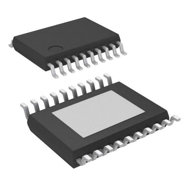
| 供应商器件封装 | 20-HTSSOP |
| 其它名称 | 296-18162-6 |
| 包装 | Digi-Reel® |
| 安装类型 | 表面贴装 |
| 封装/外壳 | 20-TSSOP(0.173",4.40mm 宽)裸焊盘 |
| 工作温度 | -40°C ~ 125°C |
| 标准包装 | 1 |
| 电压-跌落(典型值) | 0.23V @ 1A |
| 电压-输入 | 最高 10V |
| 电压-输出 | 5V |
| 电流-输出 | 1A |
| 电流-限制(最小值) | - |
| 稳压器拓扑 | 正,固定式 |
| 稳压器数 | 1 |


- 商务部:美国ITC正式对集成电路等产品启动337调查
- 曝三星4nm工艺存在良率问题 高通将骁龙8 Gen1或转产台积电
- 太阳诱电将投资9.5亿元在常州建新厂生产MLCC 预计2023年完工
- 英特尔发布欧洲新工厂建设计划 深化IDM 2.0 战略
- 台积电先进制程称霸业界 有大客户加持明年业绩稳了
- 达到5530亿美元!SIA预计今年全球半导体销售额将创下新高
- 英特尔拟将自动驾驶子公司Mobileye上市 估值或超500亿美元
- 三星加码芯片和SET,合并消费电子和移动部门,撤换高东真等 CEO
- 三星电子宣布重大人事变动 还合并消费电子和移动部门
- 海关总署:前11个月进口集成电路产品价值2.52万亿元 增长14.8%


PDF Datasheet 数据手册内容提取
(cid:1)(cid:2)(cid:3)(cid:4)(cid:5)(cid:6)(cid:7)(cid:8)(cid:9)(cid:10)(cid:2)(cid:11) (cid:1)(cid:2)(cid:3)(cid:4)(cid:5)(cid:6)(cid:7)(cid:6)(cid:9)(cid:10)(cid:2)(cid:11) (cid:1)(cid:2)(cid:3)(cid:4)(cid:5)(cid:6)(cid:12)(cid:8)(cid:9)(cid:10)(cid:2)(cid:11) (cid:1)(cid:2)(cid:3)(cid:4)(cid:5)(cid:6)(cid:12)(cid:4)(cid:9)(cid:10)(cid:2) (cid:1)(cid:2)(cid:3)(cid:4)(cid:5)(cid:6)(cid:12)(cid:6)(cid:9)(cid:10)(cid:2)(cid:11) (cid:1)(cid:2)(cid:3)(cid:4)(cid:5)(cid:6)(cid:13)(cid:14)(cid:9)(cid:10)(cid:2) (cid:1)(cid:2)(cid:3)(cid:4)(cid:5)(cid:6)(cid:13)(cid:13)(cid:9)(cid:10)(cid:2)(cid:11) (cid:1)(cid:2)(cid:3)(cid:4)(cid:5)(cid:6)(cid:8)(cid:14)(cid:9)(cid:10)(cid:2)(cid:11) (cid:1)(cid:2)(cid:3)(cid:4)(cid:5)(cid:6)(cid:14)(cid:7)(cid:9)(cid:10)(cid:2) (cid:15)(cid:16)(cid:3)(cid:1)(cid:9)(cid:1)(cid:17)(cid:16)(cid:18)(cid:3)(cid:19)(cid:10)(cid:18)(cid:1)(cid:9)(cid:17)(cid:10)(cid:3)(cid:2)(cid:20)(cid:18)(cid:3)(cid:10) (cid:7)(cid:9)(cid:16) (cid:21)(cid:20)(cid:22)(cid:9)(cid:23)(cid:17)(cid:20)(cid:2)(cid:20)(cid:24)(cid:1) (cid:25)(cid:20)(cid:21)(cid:1)(cid:16)(cid:26)(cid:10) (cid:17)(cid:10)(cid:26)(cid:24)(cid:21)(cid:16)(cid:1)(cid:20)(cid:17)(cid:3) SGLS011B − MARCH 2003 − REVISED DECEMBER 2008 FEATURES SUPPORTS DEFENSE, AEROSPACE AND (cid:1) MEDICAL APPLICATION 1−A Low-Dropout Voltage Regulator (cid:1) (cid:1) Controlled Baseline Available in 1.5-V, 1.8-V, 2.5-V, 2.7-V, 2.8-V, (cid:1) 3.0-V, 3.3-V, 5.0-V Fixed Output and One Assembly/Test Site Adjustable Versions (cid:1) One Fabrication Site (cid:1) Dropout Voltage Down to 230 mV at 1 A (cid:1) Available in Military (−55(cid:1)C/125(cid:1)C) (TPS76850) Temperature Range(cid:1) (cid:1) Ultralow 85−µA Typical Quiescent Current (cid:1) Extended Product LIfe Cycle (cid:1) Fast Transient Response (cid:1) Extended Product−Change Notification (cid:1) 2% Tolerance Over Specified Conditions for (cid:1) Product Traceability Fixed-Output Versions † Additional temperature ranges are available − contact factory. (cid:1) Open Drain Power Good (See TPS767xx for Power-On Reset With 200-ms Delay Option) PWP PACKAGE (cid:1) 20-Pin TSSOP (PWP)PowerPAD Package (TOP VIEW) (cid:1) Thermal Shutdown Protection GND/HSINK 1 20 GND/HSINK GND/HSINK 2 19 GND/HSINK description GND 3 18 NC NC 4 17 NC This device is designed to have a fast transient EN 5 16 PG response and be stable with 10-µF low ESR IN 6 15 FB/NC capacitors. This combination provides high IN 7 14 OUT performance at a reasonable cost. NC 8 13 OUT Because the PMOS device behaves as a low-value GND/HSINK 9 12 GND/HSINK resistor, the dropout voltage is very low (typically 230 GND/HSINK 10 11 GND/HSINK mV at an output current of 1 A for the TPS76850) and NC − No internal connection is directly proportional to the output current. Additionally, since the PMOS pass element is a voltage-driven device, the quiescent current is very low and independent of output loading (typically 85 µA over the full range of output current, 0 mA to 1 A). These two key specifications yield a significant improvement in operating life for battery-powered systems. This LDO family also features a sleep mode; applying a TTL high signal to EN (enable) shuts down the regulator, reducing the quiescent current to less than 1 µA at T = 25°C. J Power good (PG) is an active high output, which can be used to implement a power-on reset or a low-battery indicator. The TPS768xx is offered in 1.5-V, 1.8-V, 2.5-V, 2.7-V, 2.8-V, 3.0-V, 3.3-V, and 5.0-V fixed-voltage versions and in an adjustable version (programmable over the range of 1.2 V to 5.5 V). Output voltage tolerance is specified as a maximum of 2% over line, load, and temperature ranges. The TPS768xx family is available in a 20-pin PWP package. Please be aware that an important notice concerning availability, standard warranty, and use in critical applications of TexasInstruments semiconductor products and disclaimers thereto appears at the end of this data sheet. PowerPAD is a trademark of Texas Instruments. (cid:2)(cid:17)(cid:20)(cid:23)(cid:24)(cid:27)(cid:1)(cid:19)(cid:20)(cid:18) (cid:23)(cid:16)(cid:1)(cid:16) (cid:28)(cid:29)(cid:30)(cid:31)!"#$(cid:28)(cid:31)(cid:29) (cid:28)% &’!!((cid:29)$ #% (cid:31)(cid:30) )’*+(cid:28)&#$(cid:28)(cid:31)(cid:29) ,#$(- Copyright 2008, Texas Instruments Incorporated (cid:2)!(cid:31),’&$% &(cid:31)(cid:29)(cid:30)(cid:31)!" $(cid:31) %)(&(cid:28)(cid:30)(cid:28)&#$(cid:28)(cid:31)(cid:29)% )(! $.( $(!"% (cid:31)(cid:30) (cid:1)(/#% (cid:19)(cid:29)%$!’"((cid:29)$% %$#(cid:29),#!, 0#!!#(cid:29)$1- (cid:2)!(cid:31),’&$(cid:28)(cid:31)(cid:29) )!(cid:31)&(%%(cid:28)(cid:29)2 ,(cid:31)(% (cid:29)(cid:31)$ (cid:29)(&(%%#!(cid:28)+1 (cid:28)(cid:29)&+’,( $(%$(cid:28)(cid:29)2 (cid:31)(cid:30) #++ )#!#"($(!%- POST OFFICE BOX 655303 • DALLAS, TEXAS 75265 1
(cid:1)(cid:2)(cid:3)(cid:4)(cid:5)(cid:6)(cid:7)(cid:8)(cid:9)(cid:10)(cid:2)(cid:11) (cid:1)(cid:2)(cid:3)(cid:4)(cid:5)(cid:6)(cid:7)(cid:6)(cid:9)(cid:10)(cid:2)(cid:11) (cid:1)(cid:2)(cid:3)(cid:4)(cid:5)(cid:6)(cid:12)(cid:8)(cid:9)(cid:10)(cid:2)(cid:11) (cid:1)(cid:2)(cid:3)(cid:4)(cid:5)(cid:6)(cid:12)(cid:4)(cid:9)(cid:10)(cid:2) (cid:1)(cid:2)(cid:3)(cid:4)(cid:5)(cid:6)(cid:12)(cid:6)(cid:9)(cid:10)(cid:2)(cid:11) (cid:1)(cid:2)(cid:3)(cid:4)(cid:5)(cid:6)(cid:13)(cid:14)(cid:9)(cid:10)(cid:2) (cid:1)(cid:2)(cid:3)(cid:4)(cid:5)(cid:6)(cid:13)(cid:13)(cid:9)(cid:10)(cid:2)(cid:11) (cid:1)(cid:2)(cid:3)(cid:4)(cid:5)(cid:6)(cid:8)(cid:14)(cid:9)(cid:10)(cid:2)(cid:11) (cid:1)(cid:2)(cid:3)(cid:4)(cid:5)(cid:6)(cid:14)(cid:7)(cid:9)(cid:10)(cid:2) (cid:15)(cid:16)(cid:3)(cid:1)(cid:9)(cid:1)(cid:17)(cid:16)(cid:18)(cid:3)(cid:19)(cid:10)(cid:18)(cid:1)(cid:9)(cid:17)(cid:10)(cid:3)(cid:2)(cid:20)(cid:18)(cid:3)(cid:10) (cid:7)(cid:9)(cid:16) (cid:21)(cid:20)(cid:22)(cid:9)(cid:23)(cid:17)(cid:20)(cid:2)(cid:20)(cid:24)(cid:1) (cid:25)(cid:20)(cid:21)(cid:1)(cid:16)(cid:26)(cid:10) (cid:17)(cid:10)(cid:26)(cid:24)(cid:21)(cid:16)(cid:1)(cid:20)(cid:17)(cid:3) SGLS011B − MARCH 2003 − REVISED DECEMBER 2008 description (continued) TPS76833 DROPOUT VOLTAGE vs FREE-AIR TEMPERATURE LOAD TRANSIENT RESPONSE 103 100 V nm Co = 10 µF IO = 1 A ge ie − 50 TA = 25°C 102 anag age − mV 101 ∆V− ChOutput Volt −500 olt O V Dropout 100 IO = 10 mA ent − A −1001 − rr O u VD 10−1 ut C 0.5 p Co = 10 µF IO = 0 − Out 0 10−2 I O −60 −40 −20 0 20 40 60 80 100 120 140 0 100 200 300 400 500 600 700 800 900 1000 TA − Free-Air Temperature − °C t − Time − µs ORDERING INFORMATION† OUTPUT TJJ VOL(TVA)GE PACKAGE‡ ORDENNRUUAMMBBBLEEERR PART MMTOAAPRR-KKSIIINNDGGE TYP 5.0 TPS76850QPWPREP 76850EP 3.3 TPS76833QPWPREP 76833EP 3.0 TPS76830QPWPREP§ 76830EP§ 2.8 TPS76828QPWPREP§ 76828EP§ 2.7 TPS76827QPWPREP§ 76827EP§ −−4400°°CC ttoo 112255°°CC TTSSSSOOPP -- PPWWPP TTaappee aanndd rreeeell 2.5 TPS76825QPWPREP 76825EP 1.8 TPS76818QPWPREP 76818EP 1.5 TPS76815QPWPREP 76815EP Adjustable TPS76801QPWPREP 76801EP 1.2 V to 5.5 V Adjustable TPS76801MPWPREP 76801ME −−5555°CC ttoo 112255°CC 1.2 V to 5.5 V TTSSSSOOPP -- PPWWPP TTaappee aanndd rreeeell 5.0 TPS76850MPWPREP 76850ME †For the most current package and ordering information, see the Package Option Addendum at the end of this document, or see the TI web site at http://www.ti.com. ‡Package drawings, thermal data, and symbolization are available at http://www.ti.com/packaging. §This device is Product Preview. The TPS76801 is programmable using an external resistor divider (see application information). The PWP package is available taped and reeled. Note R suffix to the device type (e.g., TPS76801QPWPREP). 2 POST OFFICE BOX 655303 • DALLAS, TEXAS 75265
(cid:1)(cid:2)(cid:3)(cid:4)(cid:5)(cid:6)(cid:7)(cid:8)(cid:9)(cid:10)(cid:2)(cid:11) (cid:1)(cid:2)(cid:3)(cid:4)(cid:5)(cid:6)(cid:7)(cid:6)(cid:9)(cid:10)(cid:2)(cid:11) (cid:1)(cid:2)(cid:3)(cid:4)(cid:5)(cid:6)(cid:12)(cid:8)(cid:9)(cid:10)(cid:2)(cid:11) (cid:1)(cid:2)(cid:3)(cid:4)(cid:5)(cid:6)(cid:12)(cid:4)(cid:9)(cid:10)(cid:2) (cid:1)(cid:2)(cid:3)(cid:4)(cid:5)(cid:6)(cid:12)(cid:6)(cid:9)(cid:10)(cid:2)(cid:11) (cid:1)(cid:2)(cid:3)(cid:4)(cid:5)(cid:6)(cid:13)(cid:14)(cid:9)(cid:10)(cid:2) (cid:1)(cid:2)(cid:3)(cid:4)(cid:5)(cid:6)(cid:13)(cid:13)(cid:9)(cid:10)(cid:2)(cid:11) (cid:1)(cid:2)(cid:3)(cid:4)(cid:5)(cid:6)(cid:8)(cid:14)(cid:9)(cid:10)(cid:2)(cid:11) (cid:1)(cid:2)(cid:3)(cid:4)(cid:5)(cid:6)(cid:14)(cid:7)(cid:9)(cid:10)(cid:2) (cid:15)(cid:16)(cid:3)(cid:1)(cid:9)(cid:1)(cid:17)(cid:16)(cid:18)(cid:3)(cid:19)(cid:10)(cid:18)(cid:1)(cid:9)(cid:17)(cid:10)(cid:3)(cid:2)(cid:20)(cid:18)(cid:3)(cid:10) (cid:7)(cid:9)(cid:16) (cid:21)(cid:20)(cid:22)(cid:9)(cid:23)(cid:17)(cid:20)(cid:2)(cid:20)(cid:24)(cid:1) (cid:25)(cid:20)(cid:21)(cid:1)(cid:16)(cid:26)(cid:10) (cid:17)(cid:10)(cid:26)(cid:24)(cid:21)(cid:16)(cid:1)(cid:20)(cid:17)(cid:3) SGLS011B − MARCH 2003 − REVISED DECEMBER 2008 description (continued) TPS768xx 6 16 VI IN PG PG 7 IN 14 OUT VO 0.1 µF 5 13 EN OUT Co† + 10 µF GND 3 †See application information section for capacitor selection details. Figure 1. Typical Application Configuration (For Fixed Output Options) functional block diagram—adjustable version IN EN PG _ + OUT + R1 _ Vref = 1.1834 V FB/NC R2 GND External to the device POST OFFICE BOX 655303 • DALLAS, TEXAS 75265 3
(cid:1)(cid:2)(cid:3)(cid:4)(cid:5)(cid:6)(cid:7)(cid:8)(cid:9)(cid:10)(cid:2)(cid:11) (cid:1)(cid:2)(cid:3)(cid:4)(cid:5)(cid:6)(cid:7)(cid:6)(cid:9)(cid:10)(cid:2)(cid:11) (cid:1)(cid:2)(cid:3)(cid:4)(cid:5)(cid:6)(cid:12)(cid:8)(cid:9)(cid:10)(cid:2)(cid:11) (cid:1)(cid:2)(cid:3)(cid:4)(cid:5)(cid:6)(cid:12)(cid:4)(cid:9)(cid:10)(cid:2) (cid:1)(cid:2)(cid:3)(cid:4)(cid:5)(cid:6)(cid:12)(cid:6)(cid:9)(cid:10)(cid:2)(cid:11) (cid:1)(cid:2)(cid:3)(cid:4)(cid:5)(cid:6)(cid:13)(cid:14)(cid:9)(cid:10)(cid:2) (cid:1)(cid:2)(cid:3)(cid:4)(cid:5)(cid:6)(cid:13)(cid:13)(cid:9)(cid:10)(cid:2)(cid:11) (cid:1)(cid:2)(cid:3)(cid:4)(cid:5)(cid:6)(cid:8)(cid:14)(cid:9)(cid:10)(cid:2)(cid:11) (cid:1)(cid:2)(cid:3)(cid:4)(cid:5)(cid:6)(cid:14)(cid:7)(cid:9)(cid:10)(cid:2) (cid:15)(cid:16)(cid:3)(cid:1)(cid:9)(cid:1)(cid:17)(cid:16)(cid:18)(cid:3)(cid:19)(cid:10)(cid:18)(cid:1)(cid:9)(cid:17)(cid:10)(cid:3)(cid:2)(cid:20)(cid:18)(cid:3)(cid:10) (cid:7)(cid:9)(cid:16) (cid:21)(cid:20)(cid:22)(cid:9)(cid:23)(cid:17)(cid:20)(cid:2)(cid:20)(cid:24)(cid:1) (cid:25)(cid:20)(cid:21)(cid:1)(cid:16)(cid:26)(cid:10) (cid:17)(cid:10)(cid:26)(cid:24)(cid:21)(cid:16)(cid:1)(cid:20)(cid:17)(cid:3) SGLS011B − MARCH 2003 − REVISED DECEMBER 2008 functional block diagram—fixed-voltage version IN EN PG _ + OUT + _ R1 Vref = 1.1834 V R2 GND Terminal Functions PWP Package TERMINAL II//OO DDEESSCCRRIIPPTTIIOONN NAME NO. GND/HSINK 1 Ground/heatsink GND/HSINK 2 Ground/heatsink GND 3 LDO ground NC 4 No connect EN 5 I Enable input IN 6 I Input IN 7 I Input NC 8 No connect GND/HSINK 9 Ground/heatsink GND/HSINK 10 Ground/heatsink GND/HSINK 11 Ground/heatsink GND/HSINK 12 Ground/heatsink OUT 13 O Regulated output voltage OUT 14 O Regulated output voltage FB/NC 15 I Feedback input voltage for adjustable device (no connect for fixed options) PG 16 O PG output NC 17 No connect NC 18 No connect GND/HSINK 19 Ground/heatsink GND/HSINK 20 Ground/heatsink 4 POST OFFICE BOX 655303 • DALLAS, TEXAS 75265
(cid:1)(cid:2)(cid:3)(cid:4)(cid:5)(cid:6)(cid:7)(cid:8)(cid:9)(cid:10)(cid:2)(cid:11) (cid:1)(cid:2)(cid:3)(cid:4)(cid:5)(cid:6)(cid:7)(cid:6)(cid:9)(cid:10)(cid:2)(cid:11) (cid:1)(cid:2)(cid:3)(cid:4)(cid:5)(cid:6)(cid:12)(cid:8)(cid:9)(cid:10)(cid:2)(cid:11) (cid:1)(cid:2)(cid:3)(cid:4)(cid:5)(cid:6)(cid:12)(cid:4)(cid:9)(cid:10)(cid:2) (cid:1)(cid:2)(cid:3)(cid:4)(cid:5)(cid:6)(cid:12)(cid:6)(cid:9)(cid:10)(cid:2)(cid:11) (cid:1)(cid:2)(cid:3)(cid:4)(cid:5)(cid:6)(cid:13)(cid:14)(cid:9)(cid:10)(cid:2) (cid:1)(cid:2)(cid:3)(cid:4)(cid:5)(cid:6)(cid:13)(cid:13)(cid:9)(cid:10)(cid:2)(cid:11) (cid:1)(cid:2)(cid:3)(cid:4)(cid:5)(cid:6)(cid:8)(cid:14)(cid:9)(cid:10)(cid:2)(cid:11) (cid:1)(cid:2)(cid:3)(cid:4)(cid:5)(cid:6)(cid:14)(cid:7)(cid:9)(cid:10)(cid:2) (cid:15)(cid:16)(cid:3)(cid:1)(cid:9)(cid:1)(cid:17)(cid:16)(cid:18)(cid:3)(cid:19)(cid:10)(cid:18)(cid:1)(cid:9)(cid:17)(cid:10)(cid:3)(cid:2)(cid:20)(cid:18)(cid:3)(cid:10) (cid:7)(cid:9)(cid:16) (cid:21)(cid:20)(cid:22)(cid:9)(cid:23)(cid:17)(cid:20)(cid:2)(cid:20)(cid:24)(cid:1) (cid:25)(cid:20)(cid:21)(cid:1)(cid:16)(cid:26)(cid:10) (cid:17)(cid:10)(cid:26)(cid:24)(cid:21)(cid:16)(cid:1)(cid:20)(cid:17)(cid:3) SGLS011B − MARCH 2003 − REVISED DECEMBER 2008 (cid:1) absolute maximum ratings over operating free-air temperature range (unless otherwise noted) Input voltage range‡, V . . . . . . . . . . . . . . . . . . . . . . . . . . . . . . . . . . . . . . . . . . . . . . . . . . . . . . . . . . . −0.3 V to 13.5 V I Voltage range at EN . . . . . . . . . . . . . . . . . . . . . . . . . . . . . . . . . . . . . . . . . . . . . . . . . . . . . . . . . . . −0.3 V to V + 0.3 V I Maximum PG voltage . . . . . . . . . . . . . . . . . . . . . . . . . . . . . . . . . . . . . . . . . . . . . . . . . . . . . . . . . . . . . . . . . . . . . 16.5 V Peak output current . . . . . . . . . . . . . . . . . . . . . . . . . . . . . . . . . . . . . . . . . . . . . . . . . . . . . . . . . . . . . . Internally limited Continuous total power dissipation . . . . . . . . . . . . . . . . . . . . . . . . . . . . . . . . . . . . . . . See dissipation rating table Output voltage, V (OUT, FB) . . . . . . . . . . . . . . . . . . . . . . . . . . . . . . . . . . . . . . . . . . . . . . . . . . . . . . . . . . . . . . . . 7 V O Operating virtual junction temperature range, T . . . . . . . . . . . . . . . . . . . . . . . . . . . . . . . . . . . . . −40°C to 125°C J Storage temperature range, T . . . . . . . . . . . . . . . . . . . . . . . . . . . . . . . . . . . . . . . . . . . . . . . . . . . −65°C to 150°C stg ESD rating, HBM . . . . . . . . . . . . . . . . . . . . . . . . . . . . . . . . . . . . . . . . . . . . . . . . . . . . . . . . . . . . . . . . . . . . . . . . . . 2 kV †Stresses beyond those listed under “absolute maximum ratings” may cause permanent damage to the device. These are stress ratings only, and functional operation of the device at these or any other conditions beyond those indicated under “recommended operating conditions” is not implied. Exposure to absolute-maximum-rated conditions for extended periods may affect device reliability. ‡All voltage values are with respect to network terminal ground. DISSIPATION RATING TABLE − FREE-AIR TEMPERATURES AIR FLOW TA < 25°C DERATING FACTOR TA = 70°C TA = 85°C PACKAGE (CFM) POWER RATING ABOVE TA = 25°C POWER RATING POWER RATING 0 2.9 W 23.5 mW/°C 1.9 W 1.5 W PPWWPP§§ 300 4.3 W 34.6 mW/°C 2.8 W 2.2 W 0 3 W 23.8 mW/°C 1.9 W 1.5 W PPWWPP¶¶ 300 7.2 W 57.9 mW/°C 4.6 W 3.8 W §This parameter is measured with the recommended copper heat sink pattern on a 1-layer PCB, 5-in × 5-in PCB, 1 oz. copper, 2-in × 2-in coverage (4 in2). ¶This parameter is measured with the recommended copper heat sink pattern on a 8-layer PCB, 1.5-in × 2-in PCB, 1 oz. copper with layers 1, 2, 4, 5, 7, and 8 at 5% coverage (0.9 in2) and layers 3 and 6 at 100% coverage (6 in2). For more information, refer to TI technical brief SLMA002. recommended operating conditions MIN MAX UNIT Input voltage, VI# 2.7 10 V Output voltage range, VO 1.2 5.5 V Output current, IO (see Note 1) 0 1.0 A Operating virtual junction temperature, TJ (see Note 1) −40 125 °C # To calculate the minimum input voltage for your maximum output current, use the following equation: VI(min) = VO(max) + VDO(max load). NOTE 1: Continuous current and operating junction temperature are limited by internal protection circuitry, but it is not recommended that the device operate under conditions beyond those specified in this table for extended periods of time. POST OFFICE BOX 655303 • DALLAS, TEXAS 75265 5
(cid:1)(cid:2)(cid:3)(cid:4)(cid:5)(cid:6)(cid:7)(cid:8)(cid:9)(cid:10)(cid:2)(cid:11) (cid:1)(cid:2)(cid:3)(cid:4)(cid:5)(cid:6)(cid:7)(cid:6)(cid:9)(cid:10)(cid:2)(cid:11) (cid:1)(cid:2)(cid:3)(cid:4)(cid:5)(cid:6)(cid:12)(cid:8)(cid:9)(cid:10)(cid:2)(cid:11) (cid:1)(cid:2)(cid:3)(cid:4)(cid:5)(cid:6)(cid:12)(cid:4)(cid:9)(cid:10)(cid:2) (cid:1)(cid:2)(cid:3)(cid:4)(cid:5)(cid:6)(cid:12)(cid:6)(cid:9)(cid:10)(cid:2)(cid:11) (cid:1)(cid:2)(cid:3)(cid:4)(cid:5)(cid:6)(cid:13)(cid:14)(cid:9)(cid:10)(cid:2) (cid:1)(cid:2)(cid:3)(cid:4)(cid:5)(cid:6)(cid:13)(cid:13)(cid:9)(cid:10)(cid:2)(cid:11) (cid:1)(cid:2)(cid:3)(cid:4)(cid:5)(cid:6)(cid:8)(cid:14)(cid:9)(cid:10)(cid:2)(cid:11) (cid:1)(cid:2)(cid:3)(cid:4)(cid:5)(cid:6)(cid:14)(cid:7)(cid:9)(cid:10)(cid:2) (cid:15)(cid:16)(cid:3)(cid:1)(cid:9)(cid:1)(cid:17)(cid:16)(cid:18)(cid:3)(cid:19)(cid:10)(cid:18)(cid:1)(cid:9)(cid:17)(cid:10)(cid:3)(cid:2)(cid:20)(cid:18)(cid:3)(cid:10) (cid:7)(cid:9)(cid:16) (cid:21)(cid:20)(cid:22)(cid:9)(cid:23)(cid:17)(cid:20)(cid:2)(cid:20)(cid:24)(cid:1) (cid:25)(cid:20)(cid:21)(cid:1)(cid:16)(cid:26)(cid:10) (cid:17)(cid:10)(cid:26)(cid:24)(cid:21)(cid:16)(cid:1)(cid:20)(cid:17)(cid:3) SGLS011B − MARCH 2003 − REVISED DECEMBER 2008 electrical characteristics over recommended operating free-air temperature range, VI = VO(typ) + 1 V, IO = 1 mA, EN = 0 V, Co = 10 µF (unless otherwise noted) PARAMETER TEST CONDITIONS MIN TYP MAX UNIT 5.5 V ≥ VO ≥ 1.5 V, TJ = 25°C VO TTPPSS7766880011 5.5 V ≥ VO ≥ 1.5 V, TJ = −40°C to 125°C 0.98VO 1.02VO TJ = 25°C, 2.7 V < VIN < 10 V 1.5 TTPPSS7766881155 TJ = −40°C to 125°C, 2.7 V < VIN < 10 V 1.470 1.530 TJ = 25°C, 2.8 V < VIN < 10 V 1.8 TTPPSS7766881188 TJ = −40°C to 125°C, 2.8 V < VIN < 10 V 1.764 1.836 TJ = 25°C, 3.5 V < VIN < 10 V 2.5 TTPPSS7766882255 TJ = −40°C to 125°C, 3.5 V < VIN < 10 V 2.450 2.550 OOuuttppuutt vvoollttaaggee TJ = 25°C, 3.7 V < VIN < 10 V 2.7 ((1100 µµAA ttoo 11 AA llooaadd)) TTPPSS7766882277 VV ((sseeee NNoottee 22)) TJ = −40°C to 125°C, 3.7 V < VIN < 10 V 2.646 2.754 TJ = 25°C, 3.8 V < VIN < 10 V 2.8 TTPPSS7766882288 TJ = −40°C to 125°C, 3.8 V < VIN < 10 V 2.744 2.856 TJ = 25°C, 4 V < VIN < 10 V 3.0 TTPPSS7766883300 TJ = −40°C to 125°C, 4 V < VIN < 10 V 2.940 3.060 TJ = 25°C, 4.3 V < VIN < 10 V 3.3 TTPPSS7766883333 TJ = −40°C to 125°C, 4.3 V < VIN < 10 V 3.234 3.366 TJ = 25°C, 6 V < VIN < 10 V 5.0 TTPPSS7766885500 TJ = −40°C to 125°C, 6 V < VIN < 10 V 4.900 5.100 QQuuiieesscceenntt ccuurrrreenntt ((GGNNDD ccuurrrreenntt)) 10 µA < IO < 1 A, TJ = 25°C 85 µAA EN = 0V, (see Note 2) IO = 1 A, TJ = −40°C to 125°C 125 O(suetep uNto vtoelsta 2g ea nlidn e3 )regulation (∆VO/VO) VO + 1 V < VI ≤ 10 V, TJ = 25°C 0.01 %/V Load regulation 3 mV BW = 200 Hz to 100 kHz, Output noise voltage (TPS76818) 55 µVrms Co = 10 µF, IC = 1 A, TJ = 25°C Output current limit VO = 0 V 1.7 2 A Thermal shutdown junction temperature 150 °C EN = VI, TJ = 25°C, 1 µA 2.7 V < VI < 10 V SSttaannddbbyy ccuurrrreenntt EN = VI, TJ = −40°C to 125°C 10 µA 2.7 V < VI < 10 V FB input current TPS76801 FB = 1.5 V 2 nA High level enable input voltage 1.7 V Low level enable input voltage 0.9 V f = 1 KHz, Co = 10 µF, Power supply ripple rejection (see Note 2) 60 dB TJ = 25°C NOTES: 2. Minimum IN operating voltage is 2.7 V or VO(typ) + 1 V, whichever is greater. Maximum IN voltage 10 V. 3. If VO ≤ 1.8 V then VImax = 10 V, VImin = 2.7 V: (cid:2) (cid:4) V V (cid:6)2.7V LineReg.(mV) (cid:1) (cid:2)%(cid:3)V(cid:4) (cid:5) O Imax (cid:5)1000 100 If VO ≥ 2.5 V then VImax = 10 V, VImin = VO + 1 V: (cid:2) (cid:2) (cid:4)(cid:4) V V (cid:6) V (cid:7)1V O Imax O LineReg.(mV) (cid:1) (cid:2)%(cid:3)V(cid:4) (cid:5) (cid:5)1000 100 6 POST OFFICE BOX 655303 • DALLAS, TEXAS 75265
(cid:1)(cid:2)(cid:3)(cid:4)(cid:5)(cid:6)(cid:7)(cid:8)(cid:9)(cid:10)(cid:2)(cid:11) (cid:1)(cid:2)(cid:3)(cid:4)(cid:5)(cid:6)(cid:7)(cid:6)(cid:9)(cid:10)(cid:2)(cid:11) (cid:1)(cid:2)(cid:3)(cid:4)(cid:5)(cid:6)(cid:12)(cid:8)(cid:9)(cid:10)(cid:2)(cid:11) (cid:1)(cid:2)(cid:3)(cid:4)(cid:5)(cid:6)(cid:12)(cid:4)(cid:9)(cid:10)(cid:2) (cid:1)(cid:2)(cid:3)(cid:4)(cid:5)(cid:6)(cid:12)(cid:6)(cid:9)(cid:10)(cid:2)(cid:11) (cid:1)(cid:2)(cid:3)(cid:4)(cid:5)(cid:6)(cid:13)(cid:14)(cid:9)(cid:10)(cid:2) (cid:1)(cid:2)(cid:3)(cid:4)(cid:5)(cid:6)(cid:13)(cid:13)(cid:9)(cid:10)(cid:2)(cid:11) (cid:1)(cid:2)(cid:3)(cid:4)(cid:5)(cid:6)(cid:8)(cid:14)(cid:9)(cid:10)(cid:2)(cid:11) (cid:1)(cid:2)(cid:3)(cid:4)(cid:5)(cid:6)(cid:14)(cid:7)(cid:9)(cid:10)(cid:2) (cid:15)(cid:16)(cid:3)(cid:1)(cid:9)(cid:1)(cid:17)(cid:16)(cid:18)(cid:3)(cid:19)(cid:10)(cid:18)(cid:1)(cid:9)(cid:17)(cid:10)(cid:3)(cid:2)(cid:20)(cid:18)(cid:3)(cid:10) (cid:7)(cid:9)(cid:16) (cid:21)(cid:20)(cid:22)(cid:9)(cid:23)(cid:17)(cid:20)(cid:2)(cid:20)(cid:24)(cid:1) (cid:25)(cid:20)(cid:21)(cid:1)(cid:16)(cid:26)(cid:10) (cid:17)(cid:10)(cid:26)(cid:24)(cid:21)(cid:16)(cid:1)(cid:20)(cid:17)(cid:3) SGLS011B − MARCH 2003 − REVISED DECEMBER 2008 electrical characteristics over recommended operating free-air temperature range, VI = VO(typ) + 1 V, IO = 1 mA, EN = 0 V, Co = 10 µF (unless otherwise noted) (continued) PARAMETER TEST CONDITIONS MIN TYP MAX UNIT Minimum input voltage for valid PG IO(PG) = 300 µA 1.1 V Trip threshold voltage VO decreasing 92 98 %VO PPGG Hysteresis voltage Measured at VO 0.5 %VO Output low voltage VI = 2.7 V, IO(PG) = 1 mA 0.15 0.4 V Leakage current V(PG) = 5 V 1 µA EN = 0 V −1 0 1 IInnppuutt ccuurrrreenntt ((EENN)) µAA EN = VI −1 1 IO = 1 A, TJ = 25°C 500 TTPPSS7766882288 IO = 1 A, TJ = −40°C to 125°C 825 IO = 1 A, TJ = 25°C 450 TTPPSS7766883300 DDrrooppoouutt vvoollttaaggee IO = 1 A, TJ = −40°C to 125°C 675 mmVV ((sseeee NNoottee 44)) IO = 1 A, TJ = 25°C 350 TTPPSS7766883333 IO = 1 A, TJ = −40°C to 125°C 575 IO = 1 A, TJ = 25°C 230 TTPPSS7766885500 IO = 1 A, TJ = −40°C to 125°C 380 NOTE 4: IN voltage equals VO(typ) − 100 mV; TPS76801 output voltage set to 3.3 V nominal with external resistor divider. TPS76815, TPS76818, TPS76825, and TPS76827 dropout voltage limited by input voltage range limitations (i.e., TPS76830 input voltage needs to drop to 2.9 V for purpose of this test). TYPICAL CHARACTERISTICS Table of Graphs FIGURE vs Output current 2, 3, 4 VVOO OOuuttppuutt vvoollttaaggee vs Free-air temperature 5, 6, 7 Ground current vs Free-air temperature 8, 9 Power supply ripple rejection vs Frequency 10 Output spectral noise density vs Frequency 11 Input voltage (min) vs Output voltage 12 Zo Output impedance vs Frequency 13 VDO Dropout voltage vs Free-air temperature 14 Line transient response 15, 17 Load transient response 16, 18 VO Output voltage vs Time 19 Dropout voltage vs Input voltage 20 Equivalent series resistance (ESR) vs Output current 22 − 25 POST OFFICE BOX 655303 • DALLAS, TEXAS 75265 7
(cid:1)(cid:2)(cid:3)(cid:4)(cid:5)(cid:6)(cid:7)(cid:8)(cid:9)(cid:10)(cid:2)(cid:11) (cid:1)(cid:2)(cid:3)(cid:4)(cid:5)(cid:6)(cid:7)(cid:6)(cid:9)(cid:10)(cid:2)(cid:11) (cid:1)(cid:2)(cid:3)(cid:4)(cid:5)(cid:6)(cid:12)(cid:8)(cid:9)(cid:10)(cid:2)(cid:11) (cid:1)(cid:2)(cid:3)(cid:4)(cid:5)(cid:6)(cid:12)(cid:4)(cid:9)(cid:10)(cid:2) (cid:1)(cid:2)(cid:3)(cid:4)(cid:5)(cid:6)(cid:12)(cid:6)(cid:9)(cid:10)(cid:2)(cid:11) (cid:1)(cid:2)(cid:3)(cid:4)(cid:5)(cid:6)(cid:13)(cid:14)(cid:9)(cid:10)(cid:2) (cid:1)(cid:2)(cid:3)(cid:4)(cid:5)(cid:6)(cid:13)(cid:13)(cid:9)(cid:10)(cid:2)(cid:11) (cid:1)(cid:2)(cid:3)(cid:4)(cid:5)(cid:6)(cid:8)(cid:14)(cid:9)(cid:10)(cid:2)(cid:11) (cid:1)(cid:2)(cid:3)(cid:4)(cid:5)(cid:6)(cid:14)(cid:7)(cid:9)(cid:10)(cid:2) (cid:15)(cid:16)(cid:3)(cid:1)(cid:9)(cid:1)(cid:17)(cid:16)(cid:18)(cid:3)(cid:19)(cid:10)(cid:18)(cid:1)(cid:9)(cid:17)(cid:10)(cid:3)(cid:2)(cid:20)(cid:18)(cid:3)(cid:10) (cid:7)(cid:9)(cid:16) (cid:21)(cid:20)(cid:22)(cid:9)(cid:23)(cid:17)(cid:20)(cid:2)(cid:20)(cid:24)(cid:1) (cid:25)(cid:20)(cid:21)(cid:1)(cid:16)(cid:26)(cid:10) (cid:17)(cid:10)(cid:26)(cid:24)(cid:21)(cid:16)(cid:1)(cid:20)(cid:17)(cid:3) SGLS011B − MARCH 2003 − REVISED DECEMBER 2008 TYPICAL CHARACTERISTICS TPS76815 TPS76833 OUTPUT VOLTAGE OUTPUT VOLTAGE vs vs OUTPUT CURRENT OUTPUT CURRENT 1.4985 3.2835 VI = 2.7 V VTAI = = 4 2.35 °VC 1.4980 TA = 25°C 3.2830 1.4975 3.2825 V e − V ge − g a 1.4970 olta 3.2820 Volt utput V 3.2815 Output 1.4965 − O − O1.4960 O 3.2810 V V 1.4955 3.2805 1.4950 3.2800 0 0.1 0.2 0.3 0.4 0.5 0.6 0.7 0.8 0.9 1 0 0.1 0.2 0.3 0.4 0.5 0.6 0.7 0.8 0.9 1 IO − Output Current − A IO − Output Current − A Figure 2 Figure 3 TPS76825 TPS76833 OUTPUT VOLTAGE OUTPUT VOLTAGE vs vs OUTPUT CURRENT FREE-AIR TEMPERATURE 2.4960 3.32 VI = 3.5 V VI = 4.3 V 2.4955 TA = 25°C 3.31 2.4950 V V 3.30 Output Voltage − 222...444999443055 Output Voltage − 33..2298 IO = 1 A IO = 1 mA − − O O 3.27 V 2.4930 V 3.26 2.4925 2.4920 3.25 0 0.1 0.2 0.3 0.4 0.5 0.6 0.7 0.8 0.9 1 −60 −40 −20 0 20 40 60 80 100 120 140 IO − Output Current − A TA − Free-Air Temperature − °C Figure 4 Figure 5 8 POST OFFICE BOX 655303 • DALLAS, TEXAS 75265
(cid:1)(cid:2)(cid:3)(cid:4)(cid:5)(cid:6)(cid:7)(cid:8)(cid:9)(cid:10)(cid:2)(cid:11) (cid:1)(cid:2)(cid:3)(cid:4)(cid:5)(cid:6)(cid:7)(cid:6)(cid:9)(cid:10)(cid:2)(cid:11) (cid:1)(cid:2)(cid:3)(cid:4)(cid:5)(cid:6)(cid:12)(cid:8)(cid:9)(cid:10)(cid:2)(cid:11) (cid:1)(cid:2)(cid:3)(cid:4)(cid:5)(cid:6)(cid:12)(cid:4)(cid:9)(cid:10)(cid:2) (cid:1)(cid:2)(cid:3)(cid:4)(cid:5)(cid:6)(cid:12)(cid:6)(cid:9)(cid:10)(cid:2)(cid:11) (cid:1)(cid:2)(cid:3)(cid:4)(cid:5)(cid:6)(cid:13)(cid:14)(cid:9)(cid:10)(cid:2) (cid:1)(cid:2)(cid:3)(cid:4)(cid:5)(cid:6)(cid:13)(cid:13)(cid:9)(cid:10)(cid:2)(cid:11) (cid:1)(cid:2)(cid:3)(cid:4)(cid:5)(cid:6)(cid:8)(cid:14)(cid:9)(cid:10)(cid:2)(cid:11) (cid:1)(cid:2)(cid:3)(cid:4)(cid:5)(cid:6)(cid:14)(cid:7)(cid:9)(cid:10)(cid:2) (cid:15)(cid:16)(cid:3)(cid:1)(cid:9)(cid:1)(cid:17)(cid:16)(cid:18)(cid:3)(cid:19)(cid:10)(cid:18)(cid:1)(cid:9)(cid:17)(cid:10)(cid:3)(cid:2)(cid:20)(cid:18)(cid:3)(cid:10) (cid:7)(cid:9)(cid:16) (cid:21)(cid:20)(cid:22)(cid:9)(cid:23)(cid:17)(cid:20)(cid:2)(cid:20)(cid:24)(cid:1) (cid:25)(cid:20)(cid:21)(cid:1)(cid:16)(cid:26)(cid:10) (cid:17)(cid:10)(cid:26)(cid:24)(cid:21)(cid:16)(cid:1)(cid:20)(cid:17)(cid:3) SGLS011B − MARCH 2003 − REVISED DECEMBER 2008 TYPICAL CHARACTERISTICS TPS76815 TPS76825 OUTPUT VOLTAGE OUTPUT VOLTAGE vs vs FREE-AIR TEMPERATURE FREE-AIR TEMPERATURE 1.515 2.515 VI = 2.7 V VI = 3.5 V 2.510 1.510 V V 2.505 − 1.505 − e e g g a a 2.500 ut Volt 1.500 IO = 1 A ut Volt IO = 1 A p p 2.495 ut ut O IO = 1 mA O − 1.495 − IO = 1 mA O O2.490 V V 1.490 2.485 1.485 2.480 −60 −40 −20 0 20 40 60 80 100 120 140 −60 −40 −20 0 20 40 60 80 100 120 TA − Free-Air Temperature − °C TA − Free-Air Temperature − °C Figure 6 Figure 7 TPS76833 GROUND CURRENT vs FREE-AIR TEMPERATURE 92 90 VI = 4.3 V 88 86 A µ nt − 84 e rr 82 u d C 80 IO = 1 mA n ou IO = 1 A Gr 78 IO = 500 mA 76 74 72 −60 −40 −20 0 20 40 60 80 100 120 140 TA − Free-Air Temperature − °C Figure 8 POST OFFICE BOX 655303 • DALLAS, TEXAS 75265 9
(cid:1)(cid:2)(cid:3)(cid:4)(cid:5)(cid:6)(cid:7)(cid:8)(cid:9)(cid:10)(cid:2)(cid:11) (cid:1)(cid:2)(cid:3)(cid:4)(cid:5)(cid:6)(cid:7)(cid:6)(cid:9)(cid:10)(cid:2)(cid:11) (cid:1)(cid:2)(cid:3)(cid:4)(cid:5)(cid:6)(cid:12)(cid:8)(cid:9)(cid:10)(cid:2)(cid:11) (cid:1)(cid:2)(cid:3)(cid:4)(cid:5)(cid:6)(cid:12)(cid:4)(cid:9)(cid:10)(cid:2) (cid:1)(cid:2)(cid:3)(cid:4)(cid:5)(cid:6)(cid:12)(cid:6)(cid:9)(cid:10)(cid:2)(cid:11) (cid:1)(cid:2)(cid:3)(cid:4)(cid:5)(cid:6)(cid:13)(cid:14)(cid:9)(cid:10)(cid:2) (cid:1)(cid:2)(cid:3)(cid:4)(cid:5)(cid:6)(cid:13)(cid:13)(cid:9)(cid:10)(cid:2)(cid:11) (cid:1)(cid:2)(cid:3)(cid:4)(cid:5)(cid:6)(cid:8)(cid:14)(cid:9)(cid:10)(cid:2)(cid:11) (cid:1)(cid:2)(cid:3)(cid:4)(cid:5)(cid:6)(cid:14)(cid:7)(cid:9)(cid:10)(cid:2) (cid:15)(cid:16)(cid:3)(cid:1)(cid:9)(cid:1)(cid:17)(cid:16)(cid:18)(cid:3)(cid:19)(cid:10)(cid:18)(cid:1)(cid:9)(cid:17)(cid:10)(cid:3)(cid:2)(cid:20)(cid:18)(cid:3)(cid:10) (cid:7)(cid:9)(cid:16) (cid:21)(cid:20)(cid:22)(cid:9)(cid:23)(cid:17)(cid:20)(cid:2)(cid:20)(cid:24)(cid:1) (cid:25)(cid:20)(cid:21)(cid:1)(cid:16)(cid:26)(cid:10) (cid:17)(cid:10)(cid:26)(cid:24)(cid:21)(cid:16)(cid:1)(cid:20)(cid:17)(cid:3) SGLS011B − MARCH 2003 − REVISED DECEMBER 2008 TYPICAL CHARACTERISTICS TPS76815 TPS76833 GROUND CURRENT POWER SUPPLY RIPPLE REJECTION vs vs FREE-AIR TEMPERATURE FREQUENCY 100 90 B VI = 4.3 V VI = 2.7 V − d 80 Co = 10 µF n IO = 1 A 95 ctio 70 TA = 25°C e A Rej 60 µnt − 90 IO = 1 mA IO = 1 A pple 50 e Ri Curr ply 40 Ground 85 IO = 500 mA wer Sup 3200 o P 80 − 10 R R S 0 P 75 −10 −60 −40 −20 0 20 40 60 80 100 120 140 10 100 1k 10k 100k 1M TA − Free-Air Temperature − °C f − Frequency − Hz Figure 9 Figure 10 TPS76833 OUTPUT SPECTRAL NOISE DENSITY vs FREQUENCY 10−5 VI = 4.3 V z Co = 10 µF H TA = 25°C V µ sity − 10−6 IO = 7 mA n e D e s Noi IO = 1 A al r ct 10−7 e p S ut p ut O 10−8 102 103 104 105 f − Frequency − Hz Figure 11 10 POST OFFICE BOX 655303 • DALLAS, TEXAS 75265
(cid:1)(cid:2)(cid:3)(cid:4)(cid:5)(cid:6)(cid:7)(cid:8)(cid:9)(cid:10)(cid:2)(cid:11) (cid:1)(cid:2)(cid:3)(cid:4)(cid:5)(cid:6)(cid:7)(cid:6)(cid:9)(cid:10)(cid:2)(cid:11) (cid:1)(cid:2)(cid:3)(cid:4)(cid:5)(cid:6)(cid:12)(cid:8)(cid:9)(cid:10)(cid:2)(cid:11) (cid:1)(cid:2)(cid:3)(cid:4)(cid:5)(cid:6)(cid:12)(cid:4)(cid:9)(cid:10)(cid:2) (cid:1)(cid:2)(cid:3)(cid:4)(cid:5)(cid:6)(cid:12)(cid:6)(cid:9)(cid:10)(cid:2)(cid:11) (cid:1)(cid:2)(cid:3)(cid:4)(cid:5)(cid:6)(cid:13)(cid:14)(cid:9)(cid:10)(cid:2) (cid:1)(cid:2)(cid:3)(cid:4)(cid:5)(cid:6)(cid:13)(cid:13)(cid:9)(cid:10)(cid:2)(cid:11) (cid:1)(cid:2)(cid:3)(cid:4)(cid:5)(cid:6)(cid:8)(cid:14)(cid:9)(cid:10)(cid:2)(cid:11) (cid:1)(cid:2)(cid:3)(cid:4)(cid:5)(cid:6)(cid:14)(cid:7)(cid:9)(cid:10)(cid:2) (cid:15)(cid:16)(cid:3)(cid:1)(cid:9)(cid:1)(cid:17)(cid:16)(cid:18)(cid:3)(cid:19)(cid:10)(cid:18)(cid:1)(cid:9)(cid:17)(cid:10)(cid:3)(cid:2)(cid:20)(cid:18)(cid:3)(cid:10) (cid:7)(cid:9)(cid:16) (cid:21)(cid:20)(cid:22)(cid:9)(cid:23)(cid:17)(cid:20)(cid:2)(cid:20)(cid:24)(cid:1) (cid:25)(cid:20)(cid:21)(cid:1)(cid:16)(cid:26)(cid:10) (cid:17)(cid:10)(cid:26)(cid:24)(cid:21)(cid:16)(cid:1)(cid:20)(cid:17)(cid:3) SGLS011B − MARCH 2003 − REVISED DECEMBER 2008 TYPICAL CHARACTERISTICS INPUT VOLTAGE (MIN) vs OUTPUT VOLTAGE 4 IO = 1 A TA = 25°C V n) − TA = 125°C Mi e ( g 3 a olt TA = −40°C V ut p 2.7 n − I VI 2 1.5 1.75 2 2.25 2.5 2.75 3 3.25 3.5 VO − Output Voltage − V Figure 12 TPS76833 TPS76833 OUTPUT IMPEDANCE DROPOUT VOLTAGE vs vs FREQUENCY FREE-AIR TEMPERATURE 0 103 VI = 4.3 V TCAo == 2150° µCF IO = 1 A 102 V Ωmpedance − 10−1 IO = 1 mA ut Voltage − m 101 put I opo 100 IO = 10 mA ut Dr O − − O o D Z IO = 1 A V 10−1 IO = 0 Co = 10 µF 10−2 10−2 101 102 103 104 105 106 −60 −40 −20 0 20 40 60 80 100 120 140 f − Frequency − kHz TA − Free-Air Temperature − °C Figure 13 Figure 14 POST OFFICE BOX 655303 • DALLAS, TEXAS 75265 11
(cid:1)(cid:2)(cid:3)(cid:4)(cid:5)(cid:6)(cid:7)(cid:8)(cid:9)(cid:10)(cid:2)(cid:11) (cid:1)(cid:2)(cid:3)(cid:4)(cid:5)(cid:6)(cid:7)(cid:6)(cid:9)(cid:10)(cid:2)(cid:11) (cid:1)(cid:2)(cid:3)(cid:4)(cid:5)(cid:6)(cid:12)(cid:8)(cid:9)(cid:10)(cid:2)(cid:11) (cid:1)(cid:2)(cid:3)(cid:4)(cid:5)(cid:6)(cid:12)(cid:4)(cid:9)(cid:10)(cid:2) (cid:1)(cid:2)(cid:3)(cid:4)(cid:5)(cid:6)(cid:12)(cid:6)(cid:9)(cid:10)(cid:2)(cid:11) (cid:1)(cid:2)(cid:3)(cid:4)(cid:5)(cid:6)(cid:13)(cid:14)(cid:9)(cid:10)(cid:2) (cid:1)(cid:2)(cid:3)(cid:4)(cid:5)(cid:6)(cid:13)(cid:13)(cid:9)(cid:10)(cid:2)(cid:11) (cid:1)(cid:2)(cid:3)(cid:4)(cid:5)(cid:6)(cid:8)(cid:14)(cid:9)(cid:10)(cid:2)(cid:11) (cid:1)(cid:2)(cid:3)(cid:4)(cid:5)(cid:6)(cid:14)(cid:7)(cid:9)(cid:10)(cid:2) (cid:15)(cid:16)(cid:3)(cid:1)(cid:9)(cid:1)(cid:17)(cid:16)(cid:18)(cid:3)(cid:19)(cid:10)(cid:18)(cid:1)(cid:9)(cid:17)(cid:10)(cid:3)(cid:2)(cid:20)(cid:18)(cid:3)(cid:10) (cid:7)(cid:9)(cid:16) (cid:21)(cid:20)(cid:22)(cid:9)(cid:23)(cid:17)(cid:20)(cid:2)(cid:20)(cid:24)(cid:1) (cid:25)(cid:20)(cid:21)(cid:1)(cid:16)(cid:26)(cid:10) (cid:17)(cid:10)(cid:26)(cid:24)(cid:21)(cid:16)(cid:1)(cid:20)(cid:17)(cid:3) SGLS011B − MARCH 2003 − REVISED DECEMBER 2008 TYPICAL CHARACTERISTICS TPS76815 TPS76815 LINE TRANSIENT RESPONSE LOAD TRANSIENT RESPONSE 100 ge − V 3.7 e in− mV 50 CTAo == 2150° µCF nput Volta − ChangOut Voltage 0 − I 2.7 ∆Vutp −50 VI O −100 A nmV 10 nt − 1 ∆V− Change iOOutput Voltage − −100 CTAo == 2150° µCF I − Output CurreO 0.05 0 20 40 60 80 100 120 140 160 180 200 0 100 200 300 400 500 600 700 800 900 1000 t − Time − µs t − Time − µs Figure 15 Figure 16 TPS76833 TPS76833 LINE TRANSIENT RESPONSE LOAD TRANSIENT RESPONSE 100 V V − Co = 10 µF nm Co = 10 µF age TA = 25°C ge ie − 50 TA = 25°C olt anag nput V 5.3 − ChOut Volt 0 − I ∆Vutp −50 VI O 4.3 −100 A nmV 10 nt − 1 − Change iOut Voltage − −100 Output Curre 0.05 ∆VOutp I − O 0 20 40 60 80 100 120 140 160 180 200 0 100 200 300 400 500 600 700 800 900 1000 t − Time − µs t − Time − µs Figure 17 Figure 18 12 POST OFFICE BOX 655303 • DALLAS, TEXAS 75265
(cid:1)(cid:2)(cid:3)(cid:4)(cid:5)(cid:6)(cid:7)(cid:8)(cid:9)(cid:10)(cid:2)(cid:11) (cid:1)(cid:2)(cid:3)(cid:4)(cid:5)(cid:6)(cid:7)(cid:6)(cid:9)(cid:10)(cid:2)(cid:11) (cid:1)(cid:2)(cid:3)(cid:4)(cid:5)(cid:6)(cid:12)(cid:8)(cid:9)(cid:10)(cid:2)(cid:11) (cid:1)(cid:2)(cid:3)(cid:4)(cid:5)(cid:6)(cid:12)(cid:4)(cid:9)(cid:10)(cid:2) (cid:1)(cid:2)(cid:3)(cid:4)(cid:5)(cid:6)(cid:12)(cid:6)(cid:9)(cid:10)(cid:2)(cid:11) (cid:1)(cid:2)(cid:3)(cid:4)(cid:5)(cid:6)(cid:13)(cid:14)(cid:9)(cid:10)(cid:2) (cid:1)(cid:2)(cid:3)(cid:4)(cid:5)(cid:6)(cid:13)(cid:13)(cid:9)(cid:10)(cid:2)(cid:11) (cid:1)(cid:2)(cid:3)(cid:4)(cid:5)(cid:6)(cid:8)(cid:14)(cid:9)(cid:10)(cid:2)(cid:11) (cid:1)(cid:2)(cid:3)(cid:4)(cid:5)(cid:6)(cid:14)(cid:7)(cid:9)(cid:10)(cid:2) (cid:15)(cid:16)(cid:3)(cid:1)(cid:9)(cid:1)(cid:17)(cid:16)(cid:18)(cid:3)(cid:19)(cid:10)(cid:18)(cid:1)(cid:9)(cid:17)(cid:10)(cid:3)(cid:2)(cid:20)(cid:18)(cid:3)(cid:10) (cid:7)(cid:9)(cid:16) (cid:21)(cid:20)(cid:22)(cid:9)(cid:23)(cid:17)(cid:20)(cid:2)(cid:20)(cid:24)(cid:1) (cid:25)(cid:20)(cid:21)(cid:1)(cid:16)(cid:26)(cid:10) (cid:17)(cid:10)(cid:26)(cid:24)(cid:21)(cid:16)(cid:1)(cid:20)(cid:17)(cid:3) SGLS011B − MARCH 2003 − REVISED DECEMBER 2008 TYPICAL CHARACTERISTICS TPS76833 TPS76801 OUTPUT VOLTAGE DROPOUT VOLTAGE vs vs TIME (AT STARTUP) INPUT VOLTAGE 4 900 V ge − 3 ICOo = = 11 0A µF 800 IO = 1 A olta TA = 25°C ut V 2 mV 700 p − ut e 600 O 1 g − O olta 500 V V 0 pout 400 TA = 25°C TA = 125°C o r V D − − 300 e O s D ul V 200 e P TA = −40°C abl 100 n E 0 2.5 3 3.5 4 4.5 5 0 0.1 0.2 0.3 0.4 0.5 0.6 0.7 0.8 0.9 1 t − Time − ms VI − Input Voltage − V Figure 19 Figure 20 To Load VI IN OUT + Co EN RL GND ESR Figure 21. Test Circuit for Typical Regions of Stability (Figures 22 through 25) (Fixed Output Options) POST OFFICE BOX 655303 • DALLAS, TEXAS 75265 13
(cid:1)(cid:2)(cid:3)(cid:4)(cid:5)(cid:6)(cid:7)(cid:8)(cid:9)(cid:10)(cid:2)(cid:11) (cid:1)(cid:2)(cid:3)(cid:4)(cid:5)(cid:6)(cid:7)(cid:6)(cid:9)(cid:10)(cid:2)(cid:11) (cid:1)(cid:2)(cid:3)(cid:4)(cid:5)(cid:6)(cid:12)(cid:8)(cid:9)(cid:10)(cid:2)(cid:11) (cid:1)(cid:2)(cid:3)(cid:4)(cid:5)(cid:6)(cid:12)(cid:4)(cid:9)(cid:10)(cid:2) (cid:1)(cid:2)(cid:3)(cid:4)(cid:5)(cid:6)(cid:12)(cid:6)(cid:9)(cid:10)(cid:2)(cid:11) (cid:1)(cid:2)(cid:3)(cid:4)(cid:5)(cid:6)(cid:13)(cid:14)(cid:9)(cid:10)(cid:2) (cid:1)(cid:2)(cid:3)(cid:4)(cid:5)(cid:6)(cid:13)(cid:13)(cid:9)(cid:10)(cid:2)(cid:11) (cid:1)(cid:2)(cid:3)(cid:4)(cid:5)(cid:6)(cid:8)(cid:14)(cid:9)(cid:10)(cid:2)(cid:11) (cid:1)(cid:2)(cid:3)(cid:4)(cid:5)(cid:6)(cid:14)(cid:7)(cid:9)(cid:10)(cid:2) (cid:15)(cid:16)(cid:3)(cid:1)(cid:9)(cid:1)(cid:17)(cid:16)(cid:18)(cid:3)(cid:19)(cid:10)(cid:18)(cid:1)(cid:9)(cid:17)(cid:10)(cid:3)(cid:2)(cid:20)(cid:18)(cid:3)(cid:10) (cid:7)(cid:9)(cid:16) (cid:21)(cid:20)(cid:22)(cid:9)(cid:23)(cid:17)(cid:20)(cid:2)(cid:20)(cid:24)(cid:1) (cid:25)(cid:20)(cid:21)(cid:1)(cid:16)(cid:26)(cid:10) (cid:17)(cid:10)(cid:26)(cid:24)(cid:21)(cid:16)(cid:1)(cid:20)(cid:17)(cid:3) SGLS011B − MARCH 2003 − REVISED DECEMBER 2008 TYPICAL CHARACTERISTICS TYPICAL REGION OF STABILITY TYPICAL REGION OF STABILITY EQUIVALENT SERIES RESISTANCE† EQUIVALENT SERIES RESISTANCE† vs vs OUTPUT CURRENT OUTPUT CURRENT 10 10 Ω Ω − ce Region of Instability e − Region of Instability n c a n esist sista VO = 3.3 V Series R eries Re VTCJIo = == 4 14.23.75 V °µCF ent nt S 1 val 1 ale qui Region of Stability uiv SR − E R − Eq Region of Stability E VO = 3.3 V ES Co = 4.7 µF VI = 4.3 V TA = 25°C 0.1 0.1 0 200 400 600 800 1000 0 200 400 600 800 1000 IO − Output Current − mA IO − Output Current − mA Figure 22 Figure 23 TYPICAL REGION OF STABILITY TYPICAL REGION OF STABILITY EQUIVALENT SERIES RESISTANCE† EQUIVALENT SERIES RESISTANCE† vs vs OUTPUT CURRENT OUTPUT CURRENT 10 10 Ω nce − Region of Instability Ωe − Region of Instability a c Resist sistan eries es Re CVVIOo == = 42 3.23. 3 µV FV nt S 1 Seri 1 TJ = 125°C Equivale Region of Stability uivalent Region of Stability R − − Eq ES VO = 3.3 V R Co = 22 µF ES VI = 4.3 V TA = 25°C 0.1 0.1 0 200 400 600 800 1000 0 200 400 600 800 1000 IO − Output Current − mA IO − Output Current − mA Figure 24 Figure 25 †Equivalent series resistance (ESR) refers to the total series resistance, including the ESR of the capacitor, any series resistance added externally, and PWB trace resistance to Co. 14 POST OFFICE BOX 655303 • DALLAS, TEXAS 75265
(cid:1)(cid:2)(cid:3)(cid:4)(cid:5)(cid:6)(cid:7)(cid:8)(cid:9)(cid:10)(cid:2)(cid:11) (cid:1)(cid:2)(cid:3)(cid:4)(cid:5)(cid:6)(cid:7)(cid:6)(cid:9)(cid:10)(cid:2)(cid:11) (cid:1)(cid:2)(cid:3)(cid:4)(cid:5)(cid:6)(cid:12)(cid:8)(cid:9)(cid:10)(cid:2)(cid:11) (cid:1)(cid:2)(cid:3)(cid:4)(cid:5)(cid:6)(cid:12)(cid:4)(cid:9)(cid:10)(cid:2) (cid:1)(cid:2)(cid:3)(cid:4)(cid:5)(cid:6)(cid:12)(cid:6)(cid:9)(cid:10)(cid:2)(cid:11) (cid:1)(cid:2)(cid:3)(cid:4)(cid:5)(cid:6)(cid:13)(cid:14)(cid:9)(cid:10)(cid:2) (cid:1)(cid:2)(cid:3)(cid:4)(cid:5)(cid:6)(cid:13)(cid:13)(cid:9)(cid:10)(cid:2)(cid:11) (cid:1)(cid:2)(cid:3)(cid:4)(cid:5)(cid:6)(cid:8)(cid:14)(cid:9)(cid:10)(cid:2)(cid:11) (cid:1)(cid:2)(cid:3)(cid:4)(cid:5)(cid:6)(cid:14)(cid:7)(cid:9)(cid:10)(cid:2) (cid:15)(cid:16)(cid:3)(cid:1)(cid:9)(cid:1)(cid:17)(cid:16)(cid:18)(cid:3)(cid:19)(cid:10)(cid:18)(cid:1)(cid:9)(cid:17)(cid:10)(cid:3)(cid:2)(cid:20)(cid:18)(cid:3)(cid:10) (cid:7)(cid:9)(cid:16) (cid:21)(cid:20)(cid:22)(cid:9)(cid:23)(cid:17)(cid:20)(cid:2)(cid:20)(cid:24)(cid:1) (cid:25)(cid:20)(cid:21)(cid:1)(cid:16)(cid:26)(cid:10) (cid:17)(cid:10)(cid:26)(cid:24)(cid:21)(cid:16)(cid:1)(cid:20)(cid:17)(cid:3) SGLS011B − MARCH 2003 − REVISED DECEMBER 2008 APPLICATION INFORMATION The TPS768xx family includes eight fixed-output voltage regulators (1.5 V, 1.8 V, 2.5 V, 2.7 V, 2.8 V, 3.0 V, 3.3 V, and 5.0 V), and offers an adjustable device, the TPS76801 (adjustable from 1.2 V to 5.5 V). device operation The TPS768xx features very low quiescent current, which remains virtually constant even with varying loads. Conventional LDO regulators use a pnp pass element, the base current of which is directly proportional to the load current through the regulator (I = I /β). The TPS768xx uses a PMOS transistor to pass current; because B C the gate of the PMOS is voltage driven, operating current is low and invariable over the full load range. Another pitfall associated with the pnp-pass element is its tendency to saturate when the device goes into dropout. The resulting drop in β forces an increase in I to maintain the load. During power up, this translates B to large start-up currents. Systems with limited supply current may fail to start up. In battery-powered systems, it means rapid battery discharge when the voltage decays below the minimum required for regulation. The TPS768xx quiescent current remains low even when the regulator drops out, eliminating both problems. The TPS768xx family also features a shutdown mode that places the output in the high-impedance state (essentially equal to the feedback-divider resistance) and reduces quiescent current to 2 µA. If the shutdown feature is not used, EN should be tied to ground. minimum load requirements The TPS768xx family is stable even at zero load; no minimum load is required for operation. FB - pin connection (adjustable version only) The FB pin is an input pin to sense the output voltage and close the loop for the adjustable option. The output voltage is sensed through a resistor divider network to close the loop as shown in Figure 27. Normally, this connection should be as short as possible; however, the connection can be made near a critical circuit to improve performance at that point. Internally, FB connects to a high-impedance wide-bandwidth amplifier and noise pickup feeds through to the regulator output. Routing the FB connection to minimize/avoid noise pickup is essential. external capacitor requirements An input capacitor is not usually required; however, a ceramic bypass capacitor (0.047 µF or larger) improves load transient response and noise rejection if the TPS768xx is located more than a few inches from the power supply. A higher-capacitance electrolytic capacitor may be necessary if large (hundreds of milliamps) load transients with fast rise times are anticipated. Like all low dropout regulators, the TPS768xx requires an output capacitor connected between OUT and GND to stabilize the internal control loop. The minimum recommended capacitance value is 10 µF and the ESR (equivalent series resistance) must be between 50 mΩ and 1.5 Ω. Capacitor values 10 µF or larger are acceptable, provided the ESR is less than 1.5 Ω. Solid tantalum electrolytic, aluminum electrolytic, and multilayer ceramic capacitors are all suitable, provided they meet the requirements described above. Most of the commercially available 10 µF surface-mount ceramic capacitors, including devices from Sprague and Kemet, meet the ESR requirements stated above. POST OFFICE BOX 655303 • DALLAS, TEXAS 75265 15
(cid:1)(cid:2)(cid:3)(cid:4)(cid:5)(cid:6)(cid:7)(cid:8)(cid:9)(cid:10)(cid:2)(cid:11) (cid:1)(cid:2)(cid:3)(cid:4)(cid:5)(cid:6)(cid:7)(cid:6)(cid:9)(cid:10)(cid:2)(cid:11) (cid:1)(cid:2)(cid:3)(cid:4)(cid:5)(cid:6)(cid:12)(cid:8)(cid:9)(cid:10)(cid:2)(cid:11) (cid:1)(cid:2)(cid:3)(cid:4)(cid:5)(cid:6)(cid:12)(cid:4)(cid:9)(cid:10)(cid:2) (cid:1)(cid:2)(cid:3)(cid:4)(cid:5)(cid:6)(cid:12)(cid:6)(cid:9)(cid:10)(cid:2)(cid:11) (cid:1)(cid:2)(cid:3)(cid:4)(cid:5)(cid:6)(cid:13)(cid:14)(cid:9)(cid:10)(cid:2) (cid:1)(cid:2)(cid:3)(cid:4)(cid:5)(cid:6)(cid:13)(cid:13)(cid:9)(cid:10)(cid:2)(cid:11) (cid:1)(cid:2)(cid:3)(cid:4)(cid:5)(cid:6)(cid:8)(cid:14)(cid:9)(cid:10)(cid:2)(cid:11) (cid:1)(cid:2)(cid:3)(cid:4)(cid:5)(cid:6)(cid:14)(cid:7)(cid:9)(cid:10)(cid:2) (cid:15)(cid:16)(cid:3)(cid:1)(cid:9)(cid:1)(cid:17)(cid:16)(cid:18)(cid:3)(cid:19)(cid:10)(cid:18)(cid:1)(cid:9)(cid:17)(cid:10)(cid:3)(cid:2)(cid:20)(cid:18)(cid:3)(cid:10) (cid:7)(cid:9)(cid:16) (cid:21)(cid:20)(cid:22)(cid:9)(cid:23)(cid:17)(cid:20)(cid:2)(cid:20)(cid:24)(cid:1) (cid:25)(cid:20)(cid:21)(cid:1)(cid:16)(cid:26)(cid:10) (cid:17)(cid:10)(cid:26)(cid:24)(cid:21)(cid:16)(cid:1)(cid:20)(cid:17)(cid:3) SGLS011B − MARCH 2003 − REVISED DECEMBER 2008 APPLICATION INFORMATION external capacitor requirements (continued) TPS768xx 6 16 VI IN PG PG 7 IN 250 kΩ 14 OUT VO C1 0.1 µF 5 EN OUT 13 + Co 10 µF GND 3 Figure 26. Typical Application Circuit (Fixed Versions) programming the TPS76801 adjustable LDO regulator The output voltage of the TPS76801 adjustable regulator is programmed using an external resistor divider as shown in Figure 27. The output voltage is calculated using: (cid:2) (cid:4) V (cid:1)V (cid:5) 1(cid:7)R1 (1) O ref R2 Where: V = 1.1834 V typ (the internal reference voltage) ref Resistors R1 and R2 should be chosen for approximately 50-µA divider current. Lower value resistors can be used but offer no inherent advantage and waste more power. Higher values should be avoided as leakage currents at FB increase the output voltage error. The recommended design procedure is to choose R2 = 30.1kΩ to set the divider current at 50 µA and then calculate R1 using: (cid:2) (cid:4) V R1(cid:1) O (cid:6)1 (cid:5)R2 (2) V ref OUTPUT VOLTAGE TPS76801 PROGRAMMING GUIDE OUTPUT R1 R2 UNIT VI IN PG PG VOLTAGE 0.1 µF 2.5 V 33.2 30.1 kΩ ≥1.7 V 250 kΩ 3.3 V 53.6 30.1 kΩ ≤0.9 V EN OUT VO 3.6 V 61.9 30.1 kΩ R1 4.75 V 90.8 30.1 kΩ FB / NC GND R2 Figure 27. TPS76801 Adjustable LDO Regulator Programming 16 POST OFFICE BOX 655303 • DALLAS, TEXAS 75265
(cid:1)(cid:2)(cid:3)(cid:4)(cid:5)(cid:6)(cid:7)(cid:8)(cid:9)(cid:10)(cid:2)(cid:11) (cid:1)(cid:2)(cid:3)(cid:4)(cid:5)(cid:6)(cid:7)(cid:6)(cid:9)(cid:10)(cid:2)(cid:11) (cid:1)(cid:2)(cid:3)(cid:4)(cid:5)(cid:6)(cid:12)(cid:8)(cid:9)(cid:10)(cid:2)(cid:11) (cid:1)(cid:2)(cid:3)(cid:4)(cid:5)(cid:6)(cid:12)(cid:4)(cid:9)(cid:10)(cid:2) (cid:1)(cid:2)(cid:3)(cid:4)(cid:5)(cid:6)(cid:12)(cid:6)(cid:9)(cid:10)(cid:2)(cid:11) (cid:1)(cid:2)(cid:3)(cid:4)(cid:5)(cid:6)(cid:13)(cid:14)(cid:9)(cid:10)(cid:2) (cid:1)(cid:2)(cid:3)(cid:4)(cid:5)(cid:6)(cid:13)(cid:13)(cid:9)(cid:10)(cid:2)(cid:11) (cid:1)(cid:2)(cid:3)(cid:4)(cid:5)(cid:6)(cid:8)(cid:14)(cid:9)(cid:10)(cid:2)(cid:11) (cid:1)(cid:2)(cid:3)(cid:4)(cid:5)(cid:6)(cid:14)(cid:7)(cid:9)(cid:10)(cid:2) (cid:15)(cid:16)(cid:3)(cid:1)(cid:9)(cid:1)(cid:17)(cid:16)(cid:18)(cid:3)(cid:19)(cid:10)(cid:18)(cid:1)(cid:9)(cid:17)(cid:10)(cid:3)(cid:2)(cid:20)(cid:18)(cid:3)(cid:10) (cid:7)(cid:9)(cid:16) (cid:21)(cid:20)(cid:22)(cid:9)(cid:23)(cid:17)(cid:20)(cid:2)(cid:20)(cid:24)(cid:1) (cid:25)(cid:20)(cid:21)(cid:1)(cid:16)(cid:26)(cid:10) (cid:17)(cid:10)(cid:26)(cid:24)(cid:21)(cid:16)(cid:1)(cid:20)(cid:17)(cid:3) SGLS011B − MARCH 2003 − REVISED DECEMBER 2008 APPLICATION INFORMATION power-good indicator The TPS768xx features a power-good (PG) output that can be used to monitor the status of the regulator. The internal comparator monitors the output voltage: when the output drops to between 92% and 98% of its nominal regulated value, the PG output transistor turns on, taking the signal low. The open-drain output requires a pullup resistor. If not used, it can be left floating. PG can be used to drive power-on reset circuitry or used as a low-battery indicator. PG does not assert itself when the regulated output voltage falls out of the specified 2% tolerance, but instead reports an output voltage low, relative to its nominal regulated value. regulator protection The TPS768xx PMOS-pass transistor has a built-in back diode that conducts reverse currents when the input voltage drops below the output voltage (e.g., during power down). Current is conducted from the output to the input and is not internally limited. When extended reverse voltage is anticipated, external limiting may be appropriate. The TPS768xx also features internal current limiting and thermal protection. During normal operation, the TPS768xx limits output current to approximately 1.7 A. When current limiting engages, the output voltage scales back linearly until the overcurrent condition ends. While current limiting is designed to prevent gross device failure, care should be taken not to exceed the power dissipation ratings of the package. If the temperature of the device exceeds 150°C(typ), thermal-protection circuitry shuts it down. Once the device has cooled below 130°C(typ), regulator operation resumes. power dissipation and junction temperature Specified regulator operation is assured to a junction temperature of 125°C; the maximum junction temperature should be restricted to 125°C under normal operating conditions. This restriction limits the power dissipation the regulator can handle in any given application. To ensure the junction temperature is within acceptable limits, calculate the maximum allowable dissipation, P , and the actual dissipation, P , which must be less than D(max) D or equal to P . D(max) The maximum-power-dissipation limit is determined using the following equation: T max(cid:6)T P (cid:1) J A D(max) R(cid:1)JA Where: TJmax is the maximum allowable junction temperature. RθJA is the thermal resistance junction-to-ambient for the package, i.e., 172°C/W for the 8-terminal SOIC and 32.6°C/W for the 20-terminal PWP with no airflow. TA is the ambient temperature. The regulator dissipation is calculated using: (cid:2) (cid:4) P (cid:1) V (cid:6)V (cid:5)I D I O O Power dissipation resulting from quiescent current is negligible. Excessive power dissipation will trigger the thermal protection circuit. POST OFFICE BOX 655303 • DALLAS, TEXAS 75265 17
PACKAGE OPTION ADDENDUM www.ti.com 6-Feb-2020 PACKAGING INFORMATION Orderable Device Status Package Type Package Pins Package Eco Plan Lead/Ball Finish MSL Peak Temp Op Temp (°C) Device Marking Samples (1) Drawing Qty (2) (6) (3) (4/5) TPS76801MPWPREP ACTIVE HTSSOP PWP 20 2000 Green (RoHS NIPDAU Level-2-260C-1 YEAR -55 to 125 76801ME & no Sb/Br) TPS76801QPWPREP ACTIVE HTSSOP PWP 20 2000 Green (RoHS NIPDAU Level-2-260C-1 YEAR -40 to 125 76801QE & no Sb/Br) TPS76815QPWPREP ACTIVE HTSSOP PWP 20 2000 Green (RoHS NIPDAU Level-2-260C-1 YEAR -40 to 125 76815QE & no Sb/Br) TPS76818QPWPREP ACTIVE HTSSOP PWP 20 2000 Green (RoHS NIPDAU Level-2-260C-1 YEAR -40 to 125 76818QE & no Sb/Br) TPS76825QPWPREP ACTIVE HTSSOP PWP 20 2000 Green (RoHS NIPDAU Level-2-260C-1 YEAR -40 to 125 76825QE & no Sb/Br) TPS76833QPWPREP ACTIVE HTSSOP PWP 20 2000 Green (RoHS NIPDAU Level-2-260C-1 YEAR -40 to 125 76833QE & no Sb/Br) TPS76850MPWPREP ACTIVE HTSSOP PWP 20 2000 Green (RoHS NIPDAU Level-2-260C-1 YEAR -55 to 125 76850ME & no Sb/Br) TPS76850QPWPREP ACTIVE HTSSOP PWP 20 2000 Green (RoHS NIPDAU Level-2-260C-1 YEAR -40 to 125 76850QE & no Sb/Br) V62/03632-01XE ACTIVE HTSSOP PWP 20 2000 Green (RoHS NIPDAU Level-2-260C-1 YEAR -40 to 125 76801QE & no Sb/Br) V62/03632-02XE ACTIVE HTSSOP PWP 20 2000 Green (RoHS NIPDAU Level-2-260C-1 YEAR -40 to 125 76815QE & no Sb/Br) V62/03632-03XE ACTIVE HTSSOP PWP 20 2000 Green (RoHS NIPDAU Level-2-260C-1 YEAR -40 to 125 76818QE & no Sb/Br) V62/03632-04XE ACTIVE HTSSOP PWP 20 2000 Green (RoHS NIPDAU Level-2-260C-1 YEAR -40 to 125 76825QE & no Sb/Br) V62/03632-08XE ACTIVE HTSSOP PWP 20 2000 Green (RoHS NIPDAU Level-2-260C-1 YEAR -40 to 125 76833QE & no Sb/Br) V62/03632-09XE ACTIVE HTSSOP PWP 20 2000 Green (RoHS NIPDAU Level-2-260C-1 YEAR -40 to 125 76850QE & no Sb/Br) V62/03632-10XE ACTIVE HTSSOP PWP 20 2000 Green (RoHS NIPDAU Level-2-260C-1 YEAR -55 to 125 76801ME & no Sb/Br) V62/03632-11XE ACTIVE HTSSOP PWP 20 2000 Green (RoHS NIPDAU Level-2-260C-1 YEAR -55 to 125 76850ME & no Sb/Br) (1) The marketing status values are defined as follows: ACTIVE: Product device recommended for new designs. Addendum-Page 1
PACKAGE OPTION ADDENDUM www.ti.com 6-Feb-2020 LIFEBUY: TI has announced that the device will be discontinued, and a lifetime-buy period is in effect. NRND: Not recommended for new designs. Device is in production to support existing customers, but TI does not recommend using this part in a new design. PREVIEW: Device has been announced but is not in production. Samples may or may not be available. OBSOLETE: TI has discontinued the production of the device. (2) RoHS: TI defines "RoHS" to mean semiconductor products that are compliant with the current EU RoHS requirements for all 10 RoHS substances, including the requirement that RoHS substance do not exceed 0.1% by weight in homogeneous materials. Where designed to be soldered at high temperatures, "RoHS" products are suitable for use in specified lead-free processes. TI may reference these types of products as "Pb-Free". RoHS Exempt: TI defines "RoHS Exempt" to mean products that contain lead but are compliant with EU RoHS pursuant to a specific EU RoHS exemption. Green: TI defines "Green" to mean the content of Chlorine (Cl) and Bromine (Br) based flame retardants meet JS709B low halogen requirements of <=1000ppm threshold. Antimony trioxide based flame retardants must also meet the <=1000ppm threshold requirement. (3) MSL, Peak Temp. - The Moisture Sensitivity Level rating according to the JEDEC industry standard classifications, and peak solder temperature. (4) There may be additional marking, which relates to the logo, the lot trace code information, or the environmental category on the device. (5) Multiple Device Markings will be inside parentheses. Only one Device Marking contained in parentheses and separated by a "~" will appear on a device. If a line is indented then it is a continuation of the previous line and the two combined represent the entire Device Marking for that device. (6) Lead/Ball Finish - Orderable Devices may have multiple material finish options. Finish options are separated by a vertical ruled line. Lead/Ball Finish values may wrap to two lines if the finish value exceeds the maximum column width. Important Information and Disclaimer:The information provided on this page represents TI's knowledge and belief as of the date that it is provided. TI bases its knowledge and belief on information provided by third parties, and makes no representation or warranty as to the accuracy of such information. Efforts are underway to better integrate information from third parties. TI has taken and continues to take reasonable steps to provide representative and accurate information but may not have conducted destructive testing or chemical analysis on incoming materials and chemicals. TI and TI suppliers consider certain information to be proprietary, and thus CAS numbers and other limited information may not be available for release. In no event shall TI's liability arising out of such information exceed the total purchase price of the TI part(s) at issue in this document sold by TI to Customer on an annual basis. Addendum-Page 2
PACKAGE MATERIALS INFORMATION www.ti.com 12-Feb-2019 TAPE AND REEL INFORMATION *Alldimensionsarenominal Device Package Package Pins SPQ Reel Reel A0 B0 K0 P1 W Pin1 Type Drawing Diameter Width (mm) (mm) (mm) (mm) (mm) Quadrant (mm) W1(mm) TPS76801MPWPREP HTSSOP PWP 20 2000 330.0 16.4 6.95 7.1 1.6 8.0 16.0 Q1 TPS76801QPWPREP HTSSOP PWP 20 2000 330.0 16.4 6.95 7.1 1.6 8.0 16.0 Q1 TPS76815QPWPREP HTSSOP PWP 20 2000 330.0 16.4 6.95 7.1 1.6 8.0 16.0 Q1 TPS76818QPWPREP HTSSOP PWP 20 2000 330.0 16.4 6.95 7.1 1.6 8.0 16.0 Q1 TPS76825QPWPREP HTSSOP PWP 20 2000 330.0 16.4 6.95 7.1 1.6 8.0 16.0 Q1 TPS76833QPWPREP HTSSOP PWP 20 2000 330.0 16.4 6.95 7.1 1.6 8.0 16.0 Q1 TPS76850MPWPREP HTSSOP PWP 20 2000 330.0 16.4 6.95 7.1 1.6 8.0 16.0 Q1 TPS76850QPWPREP HTSSOP PWP 20 2000 330.0 16.4 6.95 7.1 1.6 8.0 16.0 Q1 PackMaterials-Page1
PACKAGE MATERIALS INFORMATION www.ti.com 12-Feb-2019 *Alldimensionsarenominal Device PackageType PackageDrawing Pins SPQ Length(mm) Width(mm) Height(mm) TPS76801MPWPREP HTSSOP PWP 20 2000 350.0 350.0 43.0 TPS76801QPWPREP HTSSOP PWP 20 2000 350.0 350.0 43.0 TPS76815QPWPREP HTSSOP PWP 20 2000 350.0 350.0 43.0 TPS76818QPWPREP HTSSOP PWP 20 2000 350.0 350.0 43.0 TPS76825QPWPREP HTSSOP PWP 20 2000 350.0 350.0 43.0 TPS76833QPWPREP HTSSOP PWP 20 2000 350.0 350.0 43.0 TPS76850MPWPREP HTSSOP PWP 20 2000 350.0 350.0 43.0 TPS76850QPWPREP HTSSOP PWP 20 2000 350.0 350.0 43.0 PackMaterials-Page2
None
None
None
None
IMPORTANTNOTICEANDDISCLAIMER TI PROVIDES TECHNICAL AND RELIABILITY DATA (INCLUDING DATASHEETS), DESIGN RESOURCES (INCLUDING REFERENCE DESIGNS), APPLICATION OR OTHER DESIGN ADVICE, WEB TOOLS, SAFETY INFORMATION, AND OTHER RESOURCES “AS IS” AND WITH ALL FAULTS, AND DISCLAIMS ALL WARRANTIES, EXPRESS AND IMPLIED, INCLUDING WITHOUT LIMITATION ANY IMPLIED WARRANTIES OF MERCHANTABILITY, FITNESS FOR A PARTICULAR PURPOSE OR NON-INFRINGEMENT OF THIRD PARTY INTELLECTUAL PROPERTY RIGHTS. These resources are intended for skilled developers designing with TI products. You are solely responsible for (1) selecting the appropriate TI products for your application, (2) designing, validating and testing your application, and (3) ensuring your application meets applicable standards, and any other safety, security, or other requirements. These resources are subject to change without notice. TI grants you permission to use these resources only for development of an application that uses the TI products described in the resource. Other reproduction and display of these resources is prohibited. No license is granted to any other TI intellectual property right or to any third party intellectual property right. TI disclaims responsibility for, and you will fully indemnify TI and its representatives against, any claims, damages, costs, losses, and liabilities arising out of your use of these resources. TI’s products are provided subject to TI’s Terms of Sale (www.ti.com/legal/termsofsale.html) or other applicable terms available either on ti.com or provided in conjunction with such TI products. TI’s provision of these resources does not expand or otherwise alter TI’s applicable warranties or warranty disclaimers for TI products. Mailing Address: Texas Instruments, Post Office Box 655303, Dallas, Texas 75265 Copyright © 2020, Texas Instruments Incorporated