ICGOO在线商城 > 集成电路(IC) > PMIC - 稳压器 - 线性 > TPS76801QD

 Datasheet下载
- 型号: TPS76801QD
- 制造商: Texas Instruments
- 库位|库存: xxxx|xxxx
- 要求:
| 数量阶梯 | 香港交货 | 国内含税 |
| +xxxx | $xxxx | ¥xxxx |
查看当月历史价格
查看今年历史价格
TPS76801QD产品简介:
ICGOO电子元器件商城为您提供TPS76801QD由Texas Instruments设计生产,在icgoo商城现货销售,并且可以通过原厂、代理商等渠道进行代购。 TPS76801QD价格参考。Texas InstrumentsTPS76801QD封装/规格:PMIC - 稳压器 - 线性, Linear Voltage Regulator IC Positive Adjustable 1 Output 1.2 V ~ 5.5 V 1A 8-SOIC。您可以下载TPS76801QD参考资料、Datasheet数据手册功能说明书,资料中有TPS76801QD 详细功能的应用电路图电压和使用方法及教程。
TPS76801QD 是 Texas Instruments(德州仪器)生产的一款线性稳压器(PMIC - Power Management IC),属于低功耗、低压差线性稳压器(LDO)。该型号的主要应用场景包括:

1. 便携式电子设备:
   TPS76801QD 的低静态电流(典型值为 15 µA)和小封装(如 SOT-23 封装)使其非常适合用于电池供电的便携式设备,例如手持终端、可穿戴设备、便携式医疗设备等。这些设备对电源效率和空间利用率要求较高。

2. 微控制器电源供应:
   该器件能够提供稳定的 1.0V 输出电压,适合为低功耗微控制器(MCU)及其外围电路供电。其输出电流能力为 150mA,足以满足大多数 MCU 和传感器的电源需求。

3. 传感器模块:
   在物联网(IoT)应用中,TPS76801QD 可以为各种传感器模块提供精确的电源支持,例如温度传感器、湿度传感器或压力传感器。其低噪声特性有助于提高传感器数据的精度。

4. 无线通信模块:
   该稳压器适用于低功耗的无线通信模块,如蓝牙、Zigbee 或 Wi-Fi 模块。它能够在保证性能的同时延长电池寿命。

5. 工业自动化设备:
   在工业领域,TPS76801QD 可用于为小型控制单元或信号调理电路供电。其宽输入电压范围(1.8V 至 5.5V)使其能够适应多种电源环境。

6. 医疗电子设备:
   对于需要高稳定性和低功耗的医疗设备,如脉搏血氧仪或血糖监测仪,TPS76801QD 的高效能和小尺寸是理想选择。

总之,TPS76801QD 的主要优势在于其低功耗、小尺寸和高稳定性,因此广泛应用于需要高效电源管理的低功耗系统中。
| 参数 | 数值 |
| 产品目录 | 集成电路 (IC)半导体 |
| 描述 | IC REG LDO ADJ 1A 8SOIC低压差稳压器 Micropower LDO Reg |
| 产品分类 | |
| 品牌 | Texas Instruments |
| 产品手册 | |
| 产品图片 |
|
| rohs | 符合RoHS无铅 / 符合限制有害物质指令(RoHS)规范要求 |
| 产品系列 | 电源管理 IC,低压差稳压器,Texas Instruments TPS76801QD- |
| 数据手册 | |
| 产品型号 | TPS76801QD |
| 产品目录页面 | |
| 产品种类 | 低压差稳压器 |
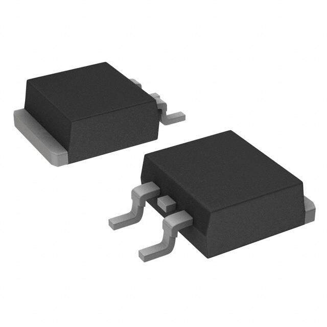
| 供应商器件封装 | 8-SOIC |
| 其它名称 | 296-2743-5 |
| 包装 | 管件 |
| 单位重量 | 76 mg |
| 参考电压 | 1.1834 V |
| 商标 | Texas Instruments |
| 安装类型 | 表面贴装 |
| 安装风格 | SMD/SMT |
| 封装 | Tube |
| 封装/外壳 | 8-SOIC(0.154",3.90mm 宽) |
| 封装/箱体 | SOIC-8 |
| 工作温度 | -40°C ~ 125°C |
| 工厂包装数量 | 75 |
| 最大功率耗散 | 0.90415 W |
| 最大工作温度 | + 125 C |
| 最大输入电压 | 10 V |
| 最小工作温度 | - 40 C |
| 最小输入电压 | + 2.7 V |
| 标准包装 | 75 |
| 电压-跌落(典型值) | 0.35V @ 1A |
| 电压-输入 | 2.7 V ~ 10 V |
| 电压-输出 | 1.2 V ~ 5.5 V |
| 电压调节准确度 | 2 % |
| 电流-输出 | 1A |
| 电流-限制(最小值) | 1.2A |
| 稳压器拓扑 | 正,可调式 |
| 稳压器数 | 1 |
| 系列 | TPS76801 |
| 线路调整率 | 0.01 % / V |
| 负载调节 | 3 mV |
| 输入偏压电流—最大 | 0.085 mA |
| 输出电压 | 1.2 V to 5.5 V |
| 输出电流 | 1 A |
| 输出端数量 | 1 Output |
| 输出类型 | Adjustable |


- 商务部:美国ITC正式对集成电路等产品启动337调查
- 曝三星4nm工艺存在良率问题 高通将骁龙8 Gen1或转产台积电
- 太阳诱电将投资9.5亿元在常州建新厂生产MLCC 预计2023年完工
- 英特尔发布欧洲新工厂建设计划 深化IDM 2.0 战略
- 台积电先进制程称霸业界 有大客户加持明年业绩稳了
- 达到5530亿美元!SIA预计今年全球半导体销售额将创下新高
- 英特尔拟将自动驾驶子公司Mobileye上市 估值或超500亿美元
- 三星加码芯片和SET,合并消费电子和移动部门,撤换高东真等 CEO
- 三星电子宣布重大人事变动 还合并消费电子和移动部门
- 海关总署:前11个月进口集成电路产品价值2.52万亿元 增长14.8%


PDF Datasheet 数据手册内容提取
TPS768xxQ www.ti.com SLVS211L–JUNE1999–REVISEDJANUARY2006 FAST TRANSIENT RESPONSE, 1-A LOW-DROPOUT VOLTAGE REGULATORS FEATURES DESCRIPTION • InputVoltageRange:2.7Vto10V This device is designed to have a fast transient • Low-DropoutVoltage:230mVtypicalat1A response and be stable with 10 m F capacitors. This (TPS76850) combination provides high performance at a reasonablecost. • 2%ToleranceOverSpecifiedConditionsfor Fixed-OutputVersions Since the PMOS device behaves as a low-value • OpenDrainPowerGood(SeeTPS767xxfor resistor, the dropout voltage is very low (typically 230mVatanoutputcurrentof1Afor the TPS76850) Power-OnResetWith200-msDelayOption) and is directly proportional to the output current. • Ultralow85m ATypicalQuiescentCurrent Additionally, because the PMOS pass element is a • Availablein1.5-V,1.8-V,2.5-V,2.7-V,2.8-V, voltage-driven device, the quiescent current is very 3.0-V,3.3-V,5.0-VFixedOutputand low and independent of output loading (typically Adjustable(1.2Vto5.5V)Versions 85 m A over the full range of output current, 0 mA to 1 A). These two key specifications yield a significant • FastTransientResponse improvement in operating life for battery-powered • ThermalShutdownProtection systems. This LDO family also features a shutdown • SOIC-8(D)andTSSOP-20(PWP)Package mode; applying a TTL high signal to EN (enable) shuts down the regulator, reducing the quiescent DPACKAGE currenttolessthan1m AatTJ=25(cid:176) C. (TopView) Power good (PG) is an active high output, which can be used to implement a power-on reset or a GND 1 8 PG low-batteryindicator. EN 2 7 FB/NC TPS768xx IN 3 6 OUT 6 16 IN 4 5 OUT VI IN PG PG 7 IN 14 OUT VO PWPPACKAGE 0.1 m F 5 13 (TopView) EN OUT Co + 10 m F GND GND/HSINK 1 20 GND/HSINK 3 GND/HSINK 2 19 GND/HSINK GND 3 18 NC NC 4 17 NC Figure1.TypicalApplicationConfiguration (ForFixedOutputOptions) EN 5 16 PG IN 6 15 FB/NC IN 7 14 OUT NC 8 13 OUT GND/HSINK 9 12 GND/HSINK GND/HSINK 10 11 GND/HSINK NC=NoInternalConnection Pleasebeawarethatanimportantnoticeconcerningavailability,standardwarranty,anduseincriticalapplicationsofTexas Instrumentssemiconductorproductsanddisclaimerstheretoappearsattheendofthisdatasheet. Alltrademarksarethepropertyoftheirrespectiveowners. PRODUCTIONDATAinformationiscurrentasofpublicationdate. Copyright©1999–2006,TexasInstrumentsIncorporated Products conform to specifications per the terms of the Texas Instruments standard warranty. Production processing does not necessarilyincludetestingofallparameters.
TPS768xxQ www.ti.com SLVS211L–JUNE1999–REVISEDJANUARY2006 This integrated circuit can be damaged by ESD. Texas Instruments recommends that all integrated circuits be handled with appropriate precautions. Failure to observe proper handling and installation procedurescancausedamage. ESD damage can range from subtle performance degradation to complete device failure. Precision integrated circuits may be more susceptible to damage because very small parametric changes could causethedevicenottomeetitspublishedspecifications. ORDERINGINFORMATION(1) PRODUCT VOUT(2) TPS768xxQyyyz XXisnominaloutputvoltage(forexample,28=2.8V,285=2.85V,01=Adjustable). YYYispackagedesignator. Zispackagequantity. (1) Forthemostcurrentpackageandorderinginformation,seethePackageOptionAddendumattheendofthisdocument,orseetheTI websiteatwww.ti.com. (2) Customoutputvoltagesareavailable;minimumorderquantitiesmayapply.Contactfactoryfordetailsandavailability. ABSOLUTE MAXIMUM RATINGS overoperatingfree-airtemperaturerange(unlessotherwisenoted) (1) VALUE Inputvoltagerange,VI(2) –0.3Vto13.5V VoltagerangeatEN –0.3VtoVI+0.3V MaximumPGvoltage 16.5V Peakoutputcurrent Internallylimited Continuoustotalpowerdissipation SeeDissipationRatingTable Outputvoltage,VO(OUT,FB) 7V Operatingjunctiontemperaturerange,TJ –40(cid:176)Cto+125(cid:176)C Storagetemperaturerange,Tstg –65(cid:176)Cto+150(cid:176)C ESDrating,HBM 2kV (1) StressesbeyondthoselistedunderAbsoluteMaximumRatingsmaycausepermanentdamagetothedevice.Thesearestressratings only,andfunctionaloperationofthedeviceattheseoranyotherconditionsbeyondthoseindicatedunderRecommendedOperating Conditionsisnotimplied.Exposuretoabsolute-maximum-ratedconditionsforextendedperiodsmayaffectdevicereliability. (2) Allvoltagevaluesarewithrespecttonetworkterminalground. DISSIPATION RATING TABLE—FREE-AIR TEMPERATURES AIRFLOW TA<+25(cid:176)C DERATINGFACTOR TA=+70(cid:176)C TA=+85(cid:176)C PACKAGE (CFM) POWERRATING ABOVETA=+25(cid:176)C POWERRATING POWERRATING 0 568.18mW 5.6818mW/(cid:176)C 312.5mW 227.27mW D 250 904.15mW 9.0415mW/(cid:176)C 497.28mW 361.66mW 0 3.1W 30.7mW/(cid:176)C 1.7W 1.2W PWP(1) 250 4.1W 41.2mW/(cid:176)C 2.3W 1.6W (1) Thisparameterismeasuredwiththerecommendedcopperheatsinkpatternona4-layer,5-in· 5-inPCB,1oz.copper,4-in· 4-in coverage(4in2). RECOMMENDED OPERATING CONDITIONS MIN MAX UNIT Inputvoltage,VI(1) 2.7 10 V Outputvoltagerange,VO 1.2 5.5 V Outputcurrent,IO(2) 0 1.0 A Operatingjunctiontemperature,TJ(2) –40 +125 (cid:176)C (1) MinimumV =V +V or2.7V,whicheverisgreater. IN OUT DO (2) Continuouscurrentandoperatingjunctiontemperaturearelimitedbyinternalprotectioncircuitry,butitisnotrecommendedthatthe deviceoperateunderconditionsbeyondthosespecifiedinthistableforextendedperiodsoftime. 2 SubmitDocumentationFeedback
TPS768xxQ www.ti.com SLVS211L–JUNE1999–REVISEDJANUARY2006 ELECTRICAL CHARACTERISTICS overrecommendedoperatingfree-airtemperaturerange,V =V +1V,I =1mA,EN=0V,C =10m F(unlessotherwise I O(typ) O O noted). PARAMETER TESTCONDITIONS MIN TYP MAX UNIT VOUTAccuracy –1400m(cid:176)AC££ ITOJ££ 1+A125(cid:176)C,VO+1V£ VIN£ 10V(1), (0.98)VO VO (1.02)VO V Quiescentcurrent(GNDcurrent)EN=0V(1) 10m A<IO<1A,TJ=+25(cid:176)C 85 m A IO=1A,TJ=–40(cid:176)Cto+125(cid:176)C 125 Outputvoltagelineregulation(D VO/VO)(1)(2) VO+1V<VI£ 10V,TJ=+25(cid:176)C 0.01 %/V Loadregulation 3 mV Outputnoisevoltage(TPS76818) BICW==12A0,0TJH=z+to251(cid:176)0C0kHz,CO=10m F, 55 m Vrms Outputcurrentlimit VO=0V 1.2 1.7 2 A Thermalshutdownjunctiontemperature 150 (cid:176)C VEN=VI,TJ=+25(cid:176)C,2.7V<VI<10V 1 m A Standbycurrent VEN=VI,TJ=–40(cid:176)Cto+125(cid:176)C, 10 m A 2.7V<VI<10V FBpincurrent,IFB TPS76801 VFB=1.5V 2 nA High-levelenableinputvoltage 1.7 V Low-levelenableinputvoltage 0.9 V Power-supplyripplerejection(1) f=1kHz,CO=10m F,TJ=+25(cid:176)C 60 dB MinimuminputvoltageforvalidPG IO(PG)=300m A 1.1 V Power Tripthresholdvoltage VOdecreasing 92 98 %VO Good Hysteresisvoltage MeasuredatVO 0.5 %VO (PG) Outputlowvoltage VI=2.7V,IO(PG)=1mA 0.15 0.4 V Leakagecurrent V(PG)=5V 1 m A Enablepincurrent(IEN) VEN=0V 1 0 1 m A VEN=VI 1 1 IO=1A,TJ=+25(cid:176)C 500 TPS76828 IO=1A,TJ=–40(cid:176)Cto+125(cid:176)C 825 IO=1A,TJ=+25(cid:176)C 450 TPS76830 Dropoutvoltage(3) IO=1A,TJ=–40(cid:176)Cto+125(cid:176)C 675 mV IO=1A,TJ=+25(cid:176)C 350 TPS76833 IO=1A,TJ=–40(cid:176)Cto+125(cid:176)C 575 IO=1A,TJ=+25(cid:176)C 230 TPS76850 IO=1A,TJ=–40(cid:176)Cto+125(cid:176)C 380 (1) MinimumINoperatingvoltageis2.7VorV +1V,whicheverisgreater.MaximumINvoltage10V. O(typ) (cid:5)VImax(cid:2)2.7V(cid:6) (2) IfV £ 1.8VthenV =10V,V =2.7V:LineReg.(mV)(cid:3)(%(cid:4)V)(cid:1)VO 100 (cid:1)1000 O Imax Imin (cid:6)VImax(cid:3)(cid:6)VO(cid:2)1V(cid:7)(cid:7) IfV ‡ 2.5VthenV =10V,V =V +1V:LineReg.(mV)(cid:4)(%(cid:5)V)(cid:1)VO 100 (cid:1)1000 O Imax Imin O (3) INvoltageequalsV (typ)–100mV;TPS76801outputvoltagesetto3.3Vnominalwithexternalresistordivider.TPS76815,TPS76818, O TPS76825,andTPS76827dropoutvoltagelimitedbyinputvoltagerangelimitations(thatis,TPS76830inputvoltagemustdropto2.9V forthepurposeofthistest). SubmitDocumentationFeedback 3
TPS768xxQ www.ti.com SLVS211L–JUNE1999–REVISEDJANUARY2006 FUNCTIONALBLOCKDIAGRAM—AdjustableVersion IN EN PG _ + OUT + R1 _ Vref = 1.1834 V FB/NC R2 GND Externaltothedevice FUNCTIONALBLOCKDIAGRAM—Fixed-VoltageVersion IN EN PG _ + OUT + _ R1 Vref = 1.1834 V R2 GND TerminalFunctions SOIC-8(D) TSSOP-20(PWP) NAME PINNO. PINNO. DESCRIPTION GND 1 3 Regulatorground GND/HSINK — 1,2,9-12,19,20 Regulatorgroundandheatsink NC — 4,8,17,18 Noconnect EN 2 5 Enableinput IN 3,4 6,7 Inputvoltage OUT 5,6 13,14 Regulatedoutputvoltage FB/NC 7 15 Feedbackinputvoltageforadjustabledevice(noconnectforfixedoptions) PG 8 16 PGoutput 4 SubmitDocumentationFeedback
TPS768xxQ www.ti.com SLVS211L–JUNE1999–REVISEDJANUARY2006 TYPICAL CHARACTERISTICS TPS76833 TPS76815 OUTPUTVOLTAGE OUTPUTVOLTAGE vs vs OUTPUTCURRENT OUTPUTCURRENT 3.2835 1.4985 VI = 4.3 V VI = 2.7 V TA = 25°C TA = 25°C 3.2830 1.4980 3.2825 1.4975 V V − − e e g g a 3.2820 a 1.4970 olt olt V V put 3.2815 put 1.4965 ut ut O O − − O 3.2810 O 1.4960 V V 3.2805 1.4955 3.2800 1.4950 0 0.1 0.2 0.3 0.4 0.5 0.6 0.7 0.8 0.9 1 0 0.1 0.2 0.3 0.4 0.5 0.6 0.7 0.8 0.9 1 IO − Output Current − A IO − Output Current − A Figure2. Figure3. TPS76825 TPS76833 OUTPUTVOLTAGE OUTPUTVOLTAGE vs vs OUTPUTCURRENT FREE-AIRTEMPERATURE 2.4960 3.32 2.4955 VTAI == 32.55° VC 3.31 VI = 4.3 V 2.4950 V V 3.30 Output Voltage − 222...444999443055 Output Voltage − 33..2289 IO = 1 A IO = 1 mA − − O O 3.27 V 2.4930 V 3.26 2.4925 2.4920 3.25 0 0.1 0.2 0.3 0.4 0.5 0.6 0.7 0.8 0.9 1 −60 −40 −20 0 20 40 60 80 100 120 140 IO − Output Current − A TA − Free-Air Temperature − °C Figure4. Figure5. SubmitDocumentationFeedback 5
TPS768xxQ www.ti.com SLVS211L–JUNE1999–REVISEDJANUARY2006 TYPICAL CHARACTERISTICS (continued) TPS76815 TPS76825 OUTPUTVOLTAGE OUTPUTVOLTAGE vs vs FREE-AIRTEMPERATURE FREE-AIRTEMPERATURE 1.515 2.515 VI = 2.7 V VI = 3.5 V 2.510 1.510 2.505 V V − 1.505 − e e g g a a 2.500 ut Volt 1.500 IO = 1 A ut Volt IO = 1 A p p 2.495 ut ut O IO = 1 mA O − O1.495 − O2.490 IO = 1 mA V V 1.490 2.485 1.485 2.480 −60 −40 −20 0 20 40 60 80 100 120 140 −60 −40 −20 0 20 40 60 80 100 120 TA − Free-Air Temperature − °C TA − Free-Air Temperature − °C Figure6. Figure7. TPS76833 TPS76815 GROUNDCURRENT GROUNDCURRENT vs vs FREE-AIRTEMPERATURE FREE-AIRTEMPERATURE 92 100 90 VI = 2.7 V VI = 4.3 V 88 95 86 A A mnt − 84 mnt − 90 IO = 1 mA IO = 1 A e e urr 82 urr ound C 80 IO = 1 A IO = 1 mA ound C 85 IO = 500 mA Gr 78 Gr IO = 500 mA 76 80 74 72 75 −60 −40 −20 0 20 40 60 80 100 120 140 −60 −40 −20 0 20 40 60 80 100 120 140 TA − Free-Air Temperature − °C TA − Free-Air Temperature − °C Figure8. Figure9. 6 SubmitDocumentationFeedback
TPS768xxQ www.ti.com SLVS211L–JUNE1999–REVISEDJANUARY2006 TYPICAL CHARACTERISTICS (continued) TPS76833 TPS76833 POWER-SUPPLYRIPPLEREJECTION OUTPUTSPECTRALNOISEDENSITY vs vs FREQUENCY FREQUENCY 90 10−5 B VI = 4.3 V VI = 4.3 V n − d 80 CIOo = = 1 1 A0 m F Hz CTAo == 2150° mCF Rejectio 7600 TA = 25°C mVy − 10−6 IO = 7 mA e sit pl 50 n y Rip 40 se De ppl Noi IO = 1 A Su 30 al er ctr 10−7 w 20 e o p P S − 10 ut R p R ut PS 0 O −10 10−8 10 100 1k 10k 100k 1M 102 103 104 105 f − Frequency − Hz f − Frequency − Hz Figure10. Figure11. TPS76833 INPUTVOLTAGE(MIN) OUTPUTIMPEDANCE vs vs OUTPUTVOLTAGE FREQUENCY 4 0 IO = 1 A VCIo = = 4 1.30 Vm F TA = 25°C TA = 25°C n) − V TA = 125°C Wce − IO = 1 mA Mi an e ( ed ag 3 mp 10−1 Volt TA = −40°C ut I put 2.7 utp n O − I − o VI Z IO = 1 A 2 10−2 1.5 1.75 2 2.25 2.5 2.75 3 3.25 3.5 101 102 103 104 105 106 VO − Output Voltage − V f − Frequency − kHz Figure12. Figure13. SubmitDocumentationFeedback 7
TPS768xxQ www.ti.com SLVS211L–JUNE1999–REVISEDJANUARY2006 TYPICAL CHARACTERISTICS (continued) TPS76833 DROPOUTVOLTAGE TPS76815 vs LINETRANSIENTRESPONSE FREE-AIRTEMPERATURE 103 V − IO = 1 A ge 3.7 a 102 olt V V m ut age − 101 − Inp 2.7 olt VI V ut po IO = 10 mA Dro 100 nmV 10 − e i− O ge D ng 0 V 10−1 Chaolta Co = 10 m F IO = 0 V− Output V −10 CTAo == 2150° mCF 10−2 D O −60 −40 −20 0 20 40 60 80 100 120 140 0 20 40 60 80 100 120 140 160 180 200 TA − Free-Air Temperature − °C t − Time − m s Figure14. Figure15. TPS76815 TPS76833 LOADTRANSIENTRESPONSE LINETRANSIENTRESPONSE 100 V V− Change inOput Voltage − mV −55000 CTAo == 2150° mCF − Input Voltage − 5.3 CTAo == 2150° mCF ut VI D O 4.3 −100 A V nt − 1 e in− m 10 e ge utput Curr 0.05 V− ChanOput Voltag −100 − O D Out I O 0 100 200 300 400 500 600 700 800 900 1000 0 20 40 60 80 100 120 140 160 180 200 t − Time − m s t − Time − m s Figure16. Figure17. 8 SubmitDocumentationFeedback
TPS768xxQ www.ti.com SLVS211L–JUNE1999–REVISEDJANUARY2006 TYPICAL CHARACTERISTICS (continued) TPS76833 TPS76833 OUTPUTVOLTAGE LOADTRANSIENTRESPONSE vs TIME(ATSTART-UP) 100 4 V− Change inOput Voltage − mV 500 CTAo == 2150° mCF utput Voltage − V 32 CITOAo = == 1 21 5A0° mCF ut −50 O 1 D O − O V −100 0 A − nt 1 e V rr − Cu 0.5 se ut ul p P Out 0 ble − na I O E 0 100 200 300 400 500 600 700 800 900 1000 0 0.1 0.2 0.3 0.4 0.5 0.6 0.7 0.8 0.9 1 t − Time − m s t − Time − ms Figure18. Figure19. TPS76801 TESTCIRCUITFORTYPICALREGIONSOFSTABILITY DROPOUTVOLTAGE (Figure22throughFigure25) vs (FixedOutputOptions) INPUTVOLTAGE 900 IO = 1 A 800 700 V m To Load e − 600 VI IN OUT g a olt 500 + pout V 400 TA = 25°C TA = 125°C EN GND Co RL o ESR Dr − 300 O D V 200 TA = −40°C 100 0 2.5 3 3.5 4 4.5 5 VI − Input Voltage − V Figure20. Figure21. SubmitDocumentationFeedback 9
TPS768xxQ www.ti.com SLVS211L–JUNE1999–REVISEDJANUARY2006 TYPICAL CHARACTERISTICS (continued) Equivalent series resistance (ESR) refers to the total series resistance, including the ESR of the capacitor, any seriesresistanceaddedexternally,andPWBtraceresistancetoC . O TYPICALREGIONOFSTABILITY TYPICALREGIONOFSTABILITY EQUIVALENTSERIESRESISTANCE EQUIVALENTSERIESRESISTANCE vs vs OUTPUTCURRENT OUTPUTCURRENT 10 10 WResistance − 1 Region of Instability WResistance − 1 Region of Instability Equivalent Series 0.1 VCVTAOIo = === 4 243.53..73° VC mVF Region of Stability Equivalent Series 0.1 VCVTJOIo = === 4 143.23..735 V °mVCF Region of Stability R − R − S S E E Region of Instability Region of Instability 0.01 0.01 0 200 400 600 800 1000 0 200 400 600 800 1000 IO − Output Current − mA IO − Output Current − mA Figure22. Figure23. TYPICALREGIONOFSTABILITY TYPICALREGIONOFSTABILITY EQUIVALENTSERIESRESISTANCE EQUIVALENTSERIESRESISTANCE vs vs OUTPUTCURRENT OUTPUTCURRENT 10 10 W Region of Instability nce − Region of Instability We − a c Resist 1 sistan 1 Equivalent Series 0.1 VCVTAOIo = === 4 223.523.3° mVC VF Region of Stability uivalent Series Re 0.1 VCVTJOIo = === 4 123.232.35 Vm °VCF Region of Stability − Eq R − ES R Region of Instability ES Region of Instability 0.01 0.01 0 200 400 600 800 1000 0 200 400 600 800 1000 IO − Output Current − mA IO − Output Current − mA Figure24. Figure25. 10 SubmitDocumentationFeedback
TPS768xxQ www.ti.com SLVS211L–JUNE1999–REVISEDJANUARY2006 APPLICATION INFORMATION The TPS768xxQ family includes eight fixed-output voltage regulators (1.5 V, 1.8 V, 2.5 V, 2.7 V, 2.8 V, 3.0 V, 3.3V,and5.0V),andoffersanadjustabledevice,theTPS76801(adjustablefrom1.2Vto5.5V). DEVICE OPERATION The TPS768xxQ features very low quiescent current, which remains virtually constant even with varying loads. Conventional LDO regulators use a PNP pass element, the base current of which is directly proportional to the load current through the regulator (I = I /b ). The TPS768xxQ uses a PMOS transistor to pass current; because B C thegateofthePMOSisvoltagedriven,operatingcurrentislowandinvariableoverthefullloadrange. Another pitfall associated with the PNP-pass element is its tendency to saturate when the device goes into dropout. The resulting drop in b forces an increase in I to maintain the load. During power up, this translates to B large start-up currents. Systems with limited supply current may fail to start up. In battery-powered systems, it means rapid battery discharge when the voltage decays below the minimum required for regulation. The TPS768xxQquiescentcurrentremainslowevenwhentheregulatordropsout,eliminatingbothproblems. The TPS768xxQ family also features a shutdown mode that places the output in the high-impedance state (essentially equal to the feedback-divider resistance) and reduces quiescent current to 2 m A. If the shutdown featureisnotused,ENshouldbetiedtoground. MINIMUM LOAD REQUIREMENTS TheTPS768xxQfamilyisstableevenatzeroload;nominimumloadisrequiredforoperation. FB - PIN CONNECTION (ADJUSTABLE VERSION ONLY) The FB pin is an input pin to sense the output voltage and close the loop for the adjustable option. The output voltage is sensed through a resistor divider network to close the loop as shown in Figure 27. Normally, this connection should be as short as possible; however, the connection can be made near a critical circuit to improve performance at that point. Internally, FB connects to a high-impedance wide-bandwidth amplifier and noise pickup feeds through to the regulator output. Routing the FB connection to minimize/avoid noise pickup is essential. EXTERNAL CAPACITOR REQUIREMENTS An input capacitor is not usually required; however, a ceramic bypass capacitor (0.047 m F or larger) improves load transient response and noise rejection if the TPS768xxQ is located more than a few inches from the power supply. A higher-capacitance electrolytic capacitor may be necessary if large (hundreds of milliamps) load transientswithfastrisetimesareanticipated. Like all low dropout regulators, the TPS768xxQ requires an output capacitor connected between OUT and GND to stabilize the internal control loop. The minimum recommended capacitance value is 10 m F and the ESR (equivalent series resistance) must be between 60 mW and 1.5 W . Capacitor values 10 m F or larger are acceptable, provided the ESR is less than 1.5W . Solid tantalum electrolytic, aluminum electrolytic, and multilayer ceramiccapacitorsareallsuitable,providedtheymeettherequirementsdescribedabove. SubmitDocumentationFeedback 11
TPS768xxQ www.ti.com SLVS211L–JUNE1999–REVISEDJANUARY2006 APPLICATION INFORMATION (continued) TPS768xx 6 16 VI IN PG PG 7 IN 250 kW 14 C1 OUT VO 0.1 m F 5 EN OUT 13 + Co 10 m F GND 3 Figure26.TypicalApplicationCircuit(FixedVersions) The output voltage of the TPS76801 adjustable regulator is programmed using an external resistor divider as showninFigure27.Theoutputvoltageiscalculatedusing: (cid:4) R1(cid:5) VO(cid:3)Vref(cid:1) 1(cid:2)R2 where: V = 1.1834 V typ (the internal reference voltage) ref (1) Resistors R1 and R2 should be chosen for approximately 50-m A divider current. Lower value resistors can be used but offer no inherent advantage and waste more power. Higher values should be avoided as leakage currents at FB increase the output voltage error. The recommended design procedure is to choose R2=30.1kW tosetthedividercurrentat50m AandthencalculateR1using: (cid:4)V (cid:5) O R1(cid:3) (cid:2)1 (cid:1)R2 V ref (2) OUTPUT VOLTAGE TPS76801 PROGRAMMING GUIDE OUTPUT R1 R2 UNIT VI IN PG PG VOLTAGE 0.1 m F 2.5 V 33.2 30.1 kW ≥ 1.7 V 250 kW 3.3 V 53.6 30.1 kW ≤ 0.9 V EN OUT VO 3.6 V 61.9 30.1 kW R1 4.75 V 90.8 30.1 kW FB / NC GND R2 Figure27.TPS76801AdjustableLDORegulatorProgramming POWER-GOOD INDICATOR The TPS768xxQ features a power-good (PG) output that can be used to monitor the status of the regulator. The internal comparator monitors the output voltage: when the output drops to between 92% and 98% of its nominal regulated value, the PG output transistor turns on, taking the signal low. The open-drain output requires a pullup resistor. If not used, it can be left floating. PG can be used to drive power-on reset circuitry or used as a low-battery indicator. PG does not assert itself when the regulated output voltage falls out of the specified 2% tolerance,butinsteadreportsanoutputvoltagelow,relativetoitsnominalregulatedvalue. 12 SubmitDocumentationFeedback
TPS768xxQ www.ti.com SLVS211L–JUNE1999–REVISEDJANUARY2006 APPLICATION INFORMATION (continued) REGULATOR PROTECTION The TPS768xxQ PMOS-pass transistor has a built-in back diode that conducts reverse currents when the input voltage drops below the output voltage (for example, during power-down). Current is conducted from the output to the input and is not internally limited. When extended reverse voltage is anticipated, external limiting may be appropriate. The TPS768xxQ also features internal current limiting and thermal protection. During normal operation, the TPS768xxQ limits output current to approximately 1.7 A. When current limiting engages, the output voltage scales back linearly until the overcurrent condition ends. While current limiting is designed to prevent gross device failure, care should be taken not to exceed the power dissipation ratings of the package. If the temperature of the device exceeds +150(cid:176) C (typ), thermal-protection circuitry shuts it down. Once the device has cooledbelow+130(cid:176) C(typ),regulatoroperationresumes. POWER DISSIPATION AND JUNCTION TEMPERATURE Specified regulator operation is assured to a junction temperature of +125(cid:176) C; the maximum junction temperature should be restricted to +125(cid:176) C under normal operating conditions. This restriction limits the power dissipation the regulator can handle in any given application. To ensure the junction temperature is within acceptable limits, calculate the maximum allowable dissipation, P max, and the actual dissipation, P , which must be less than or D D equaltoP max. D Themaximum-power-dissipationlimitisdeterminedusingthefollowingequation: T max(cid:1)T P max(cid:2) J A D R (cid:1)JA (3) Where: • T maxisthemaximumallowablejunctiontemperature. J • R is the thermal resistance junction-to-ambient for the package; that is, 172(cid:176) C/W for the 8-pin SOIC (D) q JA and32.6(cid:176) C/Wforthe20-pinTSSOP(PWP)withnoairflow. • T istheambienttemperature. A Theregulatordissipationiscalculatedusing: PD(cid:3)(cid:4)VI(cid:2)VO(cid:5)(cid:1)IO (4) Power dissipation resulting from quiescent current is negligible. Excessive power dissipation will trigger the thermalprotectioncircuit. SubmitDocumentationFeedback 13
PACKAGE OPTION ADDENDUM www.ti.com 6-Feb-2020 PACKAGING INFORMATION Orderable Device Status Package Type Package Pins Package Eco Plan Lead/Ball Finish MSL Peak Temp Op Temp (°C) Device Marking Samples (1) Drawing Qty (2) (6) (3) (4/5) TPS76801QD ACTIVE SOIC D 8 75 Green (RoHS NIPDAU Level-1-260C-UNLIM -40 to 125 76801 & no Sb/Br) TPS76801QDR ACTIVE SOIC D 8 2500 Green (RoHS NIPDAU Level-1-260C-UNLIM -40 to 125 76801 & no Sb/Br) TPS76801QDRG4 ACTIVE SOIC D 8 2500 Green (RoHS NIPDAU Level-1-260C-UNLIM -40 to 125 76801 & no Sb/Br) TPS76801QPWP ACTIVE HTSSOP PWP 20 70 Green (RoHS NIPDAU Level-2-260C-1 YEAR -40 to 125 PT76801 & no Sb/Br) TPS76801QPWPG4 ACTIVE HTSSOP PWP 20 70 Green (RoHS NIPDAU Level-2-260C-1 YEAR -40 to 125 PT76801 & no Sb/Br) TPS76801QPWPR ACTIVE HTSSOP PWP 20 2000 Green (RoHS NIPDAU Level-2-260C-1 YEAR -40 to 125 PT76801 & no Sb/Br) TPS76801QPWPRG4 ACTIVE HTSSOP PWP 20 2000 Green (RoHS NIPDAU Level-2-260C-1 YEAR -40 to 125 PT76801 & no Sb/Br) TPS76815QD ACTIVE SOIC D 8 75 Green (RoHS NIPDAU Level-1-260C-UNLIM -40 to 125 76815 & no Sb/Br) TPS76815QDR ACTIVE SOIC D 8 2500 Green (RoHS NIPDAU Level-1-260C-UNLIM -40 to 125 76815 & no Sb/Br) TPS76815QPWP ACTIVE HTSSOP PWP 20 70 Green (RoHS NIPDAU Level-2-260C-1 YEAR -40 to 125 PT76815 & no Sb/Br) TPS76815QPWPR ACTIVE HTSSOP PWP 20 2000 Green (RoHS NIPDAU Level-2-260C-1 YEAR -40 to 125 PT76815 & no Sb/Br) TPS76818QD ACTIVE SOIC D 8 75 Green (RoHS NIPDAU Level-1-260C-UNLIM -40 to 125 76818 & no Sb/Br) TPS76818QDR ACTIVE SOIC D 8 2500 Green (RoHS NIPDAU Level-1-260C-UNLIM -40 to 125 76818 & no Sb/Br) TPS76818QDRG4 ACTIVE SOIC D 8 2500 Green (RoHS NIPDAU Level-1-260C-UNLIM -40 to 125 76818 & no Sb/Br) TPS76818QPWP ACTIVE HTSSOP PWP 20 70 Green (RoHS NIPDAU Level-2-260C-1 YEAR -40 to 125 PT76818 & no Sb/Br) TPS76818QPWPR ACTIVE HTSSOP PWP 20 2000 Green (RoHS NIPDAU Level-2-260C-1 YEAR -40 to 125 PT76818 & no Sb/Br) TPS76825QD ACTIVE SOIC D 8 75 Green (RoHS NIPDAU Level-1-260C-UNLIM -40 to 125 76825 & no Sb/Br) Addendum-Page 1
PACKAGE OPTION ADDENDUM www.ti.com 6-Feb-2020 Orderable Device Status Package Type Package Pins Package Eco Plan Lead/Ball Finish MSL Peak Temp Op Temp (°C) Device Marking Samples (1) Drawing Qty (2) (6) (3) (4/5) TPS76825QDG4 ACTIVE SOIC D 8 75 Green (RoHS NIPDAU Level-1-260C-UNLIM -40 to 125 76825 & no Sb/Br) TPS76825QDR ACTIVE SOIC D 8 2500 Green (RoHS NIPDAU Level-1-260C-UNLIM -40 to 125 76825 & no Sb/Br) TPS76825QPWP ACTIVE HTSSOP PWP 20 70 Green (RoHS NIPDAU Level-2-260C-1 YEAR -40 to 125 PT76825 & no Sb/Br) TPS76825QPWPR ACTIVE HTSSOP PWP 20 2000 Green (RoHS NIPDAU Level-2-260C-1 YEAR -40 to 125 PT76825 & no Sb/Br) TPS76825QPWPRG4 ACTIVE HTSSOP PWP 20 2000 Green (RoHS NIPDAU Level-2-260C-1 YEAR -40 to 125 PT76825 & no Sb/Br) TPS76827QD ACTIVE SOIC D 8 75 Green (RoHS NIPDAU Level-1-260C-UNLIM -40 to 125 76827 & no Sb/Br) TPS76828QD ACTIVE SOIC D 8 75 Green (RoHS NIPDAU Level-1-260C-UNLIM -40 to 125 76828 & no Sb/Br) TPS76830QD ACTIVE SOIC D 8 75 Green (RoHS NIPDAU Level-1-260C-UNLIM -40 to 125 76830 & no Sb/Br) TPS76830QPWP ACTIVE HTSSOP PWP 20 70 Green (RoHS NIPDAU Level-2-260C-1 YEAR -40 to 125 PT76830 & no Sb/Br) TPS76833QD ACTIVE SOIC D 8 75 Green (RoHS NIPDAU Level-1-260C-UNLIM -40 to 125 76833 & no Sb/Br) TPS76833QDR ACTIVE SOIC D 8 2500 Green (RoHS NIPDAU Level-1-260C-UNLIM -40 to 125 76833 & no Sb/Br) TPS76833QDRG4 ACTIVE SOIC D 8 2500 Green (RoHS NIPDAU Level-1-260C-UNLIM -40 to 125 76833 & no Sb/Br) TPS76833QPWP ACTIVE HTSSOP PWP 20 70 Green (RoHS NIPDAU Level-2-260C-1 YEAR -40 to 125 PT76833 & no Sb/Br) TPS76833QPWPG4 ACTIVE HTSSOP PWP 20 70 Green (RoHS NIPDAU Level-2-260C-1 YEAR -40 to 125 PT76833 & no Sb/Br) TPS76833QPWPR ACTIVE HTSSOP PWP 20 2000 Green (RoHS NIPDAU Level-2-260C-1 YEAR -40 to 125 PT76833 & no Sb/Br) TPS76833QPWPRG4 ACTIVE HTSSOP PWP 20 2000 Green (RoHS NIPDAU Level-2-260C-1 YEAR -40 to 125 PT76833 & no Sb/Br) TPS76850QD ACTIVE SOIC D 8 75 Green (RoHS NIPDAU Level-1-260C-UNLIM -40 to 125 76850 & no Sb/Br) TPS76850QDG4 ACTIVE SOIC D 8 75 Green (RoHS NIPDAU Level-1-260C-UNLIM -40 to 125 76850 & no Sb/Br) Addendum-Page 2
PACKAGE OPTION ADDENDUM www.ti.com 6-Feb-2020 Orderable Device Status Package Type Package Pins Package Eco Plan Lead/Ball Finish MSL Peak Temp Op Temp (°C) Device Marking Samples (1) Drawing Qty (2) (6) (3) (4/5) TPS76850QDR ACTIVE SOIC D 8 2500 Green (RoHS NIPDAU Level-1-260C-UNLIM -40 to 125 76850 & no Sb/Br) TPS76850QPWP ACTIVE HTSSOP PWP 20 70 Green (RoHS NIPDAU Level-2-260C-1 YEAR -40 to 125 PT76850 & no Sb/Br) TPS76850QPWPR ACTIVE HTSSOP PWP 20 2000 Green (RoHS NIPDAU Level-2-260C-1 YEAR -40 to 125 PT76850 & no Sb/Br) (1) The marketing status values are defined as follows: ACTIVE: Product device recommended for new designs. LIFEBUY: TI has announced that the device will be discontinued, and a lifetime-buy period is in effect. NRND: Not recommended for new designs. Device is in production to support existing customers, but TI does not recommend using this part in a new design. PREVIEW: Device has been announced but is not in production. Samples may or may not be available. OBSOLETE: TI has discontinued the production of the device. (2) RoHS: TI defines "RoHS" to mean semiconductor products that are compliant with the current EU RoHS requirements for all 10 RoHS substances, including the requirement that RoHS substance do not exceed 0.1% by weight in homogeneous materials. Where designed to be soldered at high temperatures, "RoHS" products are suitable for use in specified lead-free processes. TI may reference these types of products as "Pb-Free". RoHS Exempt: TI defines "RoHS Exempt" to mean products that contain lead but are compliant with EU RoHS pursuant to a specific EU RoHS exemption. Green: TI defines "Green" to mean the content of Chlorine (Cl) and Bromine (Br) based flame retardants meet JS709B low halogen requirements of <=1000ppm threshold. Antimony trioxide based flame retardants must also meet the <=1000ppm threshold requirement. (3) MSL, Peak Temp. - The Moisture Sensitivity Level rating according to the JEDEC industry standard classifications, and peak solder temperature. (4) There may be additional marking, which relates to the logo, the lot trace code information, or the environmental category on the device. (5) Multiple Device Markings will be inside parentheses. Only one Device Marking contained in parentheses and separated by a "~" will appear on a device. If a line is indented then it is a continuation of the previous line and the two combined represent the entire Device Marking for that device. (6) Lead/Ball Finish - Orderable Devices may have multiple material finish options. Finish options are separated by a vertical ruled line. Lead/Ball Finish values may wrap to two lines if the finish value exceeds the maximum column width. Important Information and Disclaimer:The information provided on this page represents TI's knowledge and belief as of the date that it is provided. TI bases its knowledge and belief on information provided by third parties, and makes no representation or warranty as to the accuracy of such information. Efforts are underway to better integrate information from third parties. TI has taken and continues to take reasonable steps to provide representative and accurate information but may not have conducted destructive testing or chemical analysis on incoming materials and chemicals. TI and TI suppliers consider certain information to be proprietary, and thus CAS numbers and other limited information may not be available for release. In no event shall TI's liability arising out of such information exceed the total purchase price of the TI part(s) at issue in this document sold by TI to Customer on an annual basis. Addendum-Page 3
PACKAGE OPTION ADDENDUM www.ti.com 6-Feb-2020 OTHER QUALIFIED VERSIONS OF TPS768 : •Automotive: TPS768-Q1 NOTE: Qualified Version Definitions: •Automotive - Q100 devices qualified for high-reliability automotive applications targeting zero defects Addendum-Page 4
PACKAGE MATERIALS INFORMATION www.ti.com 20-Feb-2019 TAPE AND REEL INFORMATION *Alldimensionsarenominal Device Package Package Pins SPQ Reel Reel A0 B0 K0 P1 W Pin1 Type Drawing Diameter Width (mm) (mm) (mm) (mm) (mm) Quadrant (mm) W1(mm) TPS76801QDR SOIC D 8 2500 330.0 12.4 6.4 5.2 2.1 8.0 12.0 Q1 TPS76801QPWPR HTSSOP PWP 20 2000 330.0 16.4 6.95 7.1 1.6 8.0 16.0 Q1 TPS76815QDR SOIC D 8 2500 330.0 12.4 6.4 5.2 2.1 8.0 12.0 Q1 TPS76815QPWPR HTSSOP PWP 20 2000 330.0 16.4 6.95 7.1 1.6 8.0 16.0 Q1 TPS76818QDR SOIC D 8 2500 330.0 12.4 6.4 5.2 2.1 8.0 12.0 Q1 TPS76818QPWPR HTSSOP PWP 20 2000 330.0 16.4 6.95 7.1 1.6 8.0 16.0 Q1 TPS76825QDR SOIC D 8 2500 330.0 12.4 6.4 5.2 2.1 8.0 12.0 Q1 TPS76825QPWPR HTSSOP PWP 20 2000 330.0 16.4 6.95 7.1 1.6 8.0 16.0 Q1 TPS76833QDR SOIC D 8 2500 330.0 12.4 6.4 5.2 2.1 8.0 12.0 Q1 TPS76833QPWPR HTSSOP PWP 20 2000 330.0 16.4 6.95 7.1 1.6 8.0 16.0 Q1 TPS76850QDR SOIC D 8 2500 330.0 12.4 6.4 5.2 2.1 8.0 12.0 Q1 TPS76850QPWPR HTSSOP PWP 20 2000 330.0 16.4 6.95 7.1 1.6 8.0 16.0 Q1 PackMaterials-Page1
PACKAGE MATERIALS INFORMATION www.ti.com 20-Feb-2019 *Alldimensionsarenominal Device PackageType PackageDrawing Pins SPQ Length(mm) Width(mm) Height(mm) TPS76801QDR SOIC D 8 2500 367.0 367.0 35.0 TPS76801QPWPR HTSSOP PWP 20 2000 350.0 350.0 43.0 TPS76815QDR SOIC D 8 2500 350.0 350.0 43.0 TPS76815QPWPR HTSSOP PWP 20 2000 350.0 350.0 43.0 TPS76818QDR SOIC D 8 2500 350.0 350.0 43.0 TPS76818QPWPR HTSSOP PWP 20 2000 350.0 350.0 43.0 TPS76825QDR SOIC D 8 2500 350.0 350.0 43.0 TPS76825QPWPR HTSSOP PWP 20 2000 350.0 350.0 43.0 TPS76833QDR SOIC D 8 2500 350.0 350.0 43.0 TPS76833QPWPR HTSSOP PWP 20 2000 350.0 350.0 43.0 TPS76850QDR SOIC D 8 2500 350.0 350.0 43.0 TPS76850QPWPR HTSSOP PWP 20 2000 350.0 350.0 43.0 PackMaterials-Page2
PACKAGE OUTLINE D0008A SOIC - 1.75 mm max height SCALE 2.800 SMALL OUTLINE INTEGRATED CIRCUIT C SEATING PLANE .228-.244 TYP [5.80-6.19] .004 [0.1] C A PIN 1 ID AREA 6X .050 [1.27] 8 1 2X .189-.197 [4.81-5.00] .150 NOTE 3 [3.81] 4X (0 -15 ) 4 5 8X .012-.020 B .150-.157 [0.31-0.51] .069 MAX [3.81-3.98] .010 [0.25] C A B [1.75] NOTE 4 .005-.010 TYP [0.13-0.25] 4X (0 -15 ) SEE DETAIL A .010 [0.25] .004-.010 0 - 8 [0.11-0.25] .016-.050 [0.41-1.27] DETAIL A (.041) TYPICAL [1.04] 4214825/C 02/2019 NOTES: 1. Linear dimensions are in inches [millimeters]. Dimensions in parenthesis are for reference only. Controlling dimensions are in inches. Dimensioning and tolerancing per ASME Y14.5M. 2. This drawing is subject to change without notice. 3. This dimension does not include mold flash, protrusions, or gate burrs. Mold flash, protrusions, or gate burrs shall not exceed .006 [0.15] per side. 4. This dimension does not include interlead flash. 5. Reference JEDEC registration MS-012, variation AA. www.ti.com
EXAMPLE BOARD LAYOUT D0008A SOIC - 1.75 mm max height SMALL OUTLINE INTEGRATED CIRCUIT 8X (.061 ) [1.55] SYMM SEE DETAILS 1 8 8X (.024) [0.6] SYMM (R.002 ) TYP [0.05] 5 4 6X (.050 ) [1.27] (.213) [5.4] LAND PATTERN EXAMPLE EXPOSED METAL SHOWN SCALE:8X SOLDER MASK SOLDER MASK METAL OPENING OPENING METAL UNDER SOLDER MASK EXPOSED METAL EXPOSED METAL .0028 MAX .0028 MIN [0.07] [0.07] ALL AROUND ALL AROUND NON SOLDER MASK SOLDER MASK DEFINED DEFINED SOLDER MASK DETAILS 4214825/C 02/2019 NOTES: (continued) 6. Publication IPC-7351 may have alternate designs. 7. Solder mask tolerances between and around signal pads can vary based on board fabrication site. www.ti.com
EXAMPLE STENCIL DESIGN D0008A SOIC - 1.75 mm max height SMALL OUTLINE INTEGRATED CIRCUIT 8X (.061 ) [1.55] SYMM 1 8 8X (.024) [0.6] SYMM (R.002 ) TYP [0.05] 5 4 6X (.050 ) [1.27] (.213) [5.4] SOLDER PASTE EXAMPLE BASED ON .005 INCH [0.125 MM] THICK STENCIL SCALE:8X 4214825/C 02/2019 NOTES: (continued) 8. Laser cutting apertures with trapezoidal walls and rounded corners may offer better paste release. IPC-7525 may have alternate design recommendations. 9. Board assembly site may have different recommendations for stencil design. www.ti.com
None
None
None
None
IMPORTANTNOTICEANDDISCLAIMER TI PROVIDES TECHNICAL AND RELIABILITY DATA (INCLUDING DATASHEETS), DESIGN RESOURCES (INCLUDING REFERENCE DESIGNS), APPLICATION OR OTHER DESIGN ADVICE, WEB TOOLS, SAFETY INFORMATION, AND OTHER RESOURCES “AS IS” AND WITH ALL FAULTS, AND DISCLAIMS ALL WARRANTIES, EXPRESS AND IMPLIED, INCLUDING WITHOUT LIMITATION ANY IMPLIED WARRANTIES OF MERCHANTABILITY, FITNESS FOR A PARTICULAR PURPOSE OR NON-INFRINGEMENT OF THIRD PARTY INTELLECTUAL PROPERTY RIGHTS. These resources are intended for skilled developers designing with TI products. You are solely responsible for (1) selecting the appropriate TI products for your application, (2) designing, validating and testing your application, and (3) ensuring your application meets applicable standards, and any other safety, security, or other requirements. These resources are subject to change without notice. TI grants you permission to use these resources only for development of an application that uses the TI products described in the resource. Other reproduction and display of these resources is prohibited. No license is granted to any other TI intellectual property right or to any third party intellectual property right. TI disclaims responsibility for, and you will fully indemnify TI and its representatives against, any claims, damages, costs, losses, and liabilities arising out of your use of these resources. TI’s products are provided subject to TI’s Terms of Sale (www.ti.com/legal/termsofsale.html) or other applicable terms available either on ti.com or provided in conjunction with such TI products. TI’s provision of these resources does not expand or otherwise alter TI’s applicable warranties or warranty disclaimers for TI products. Mailing Address: Texas Instruments, Post Office Box 655303, Dallas, Texas 75265 Copyright © 2020, Texas Instruments Incorporated