ICGOO在线商城 > 集成电路(IC) > PMIC - 稳压器 - 线性 > TPS75101QPWP
 Datasheet下载
- 型号: TPS75101QPWP
- 制造商: Texas Instruments
- 库位|库存: xxxx|xxxx
- 要求:
| 数量阶梯 | 香港交货 | 国内含税 |
| +xxxx | $xxxx | ¥xxxx |
查看当月历史价格
查看今年历史价格
TPS75101QPWP产品简介:
ICGOO电子元器件商城为您提供TPS75101QPWP由Texas Instruments设计生产,在icgoo商城现货销售,并且可以通过原厂、代理商等渠道进行代购。 TPS75101QPWP价格参考¥10.90-¥31.00。Texas InstrumentsTPS75101QPWP封装/规格:PMIC - 稳压器 - 线性, Linear Voltage Regulator IC Positive Adjustable 1 Output 1.5 V ~ 5 V 1.5A 20-HTSSOP。您可以下载TPS75101QPWP参考资料、Datasheet数据手册功能说明书,资料中有TPS75101QPWP 详细功能的应用电路图电压和使用方法及教程。
TPS75101QPWP 是 Texas Instruments(德州仪器)推出的一款 PMIC(电源管理集成电路),属于线性稳压器系列。其主要应用场景包括:

 1. 便携式电子设备
   - TPS75101QPWP 的低功耗特性和小封装设计使其非常适合便携式设备,例如手持终端、移动医疗设备和物联网(IoT)传感器节点。这些设备通常需要高效的电源管理和较小的占板面积。

 2. 工业自动化
   - 在工业应用中,该芯片可用于为微控制器、传感器和其他低功耗组件供电。其高精度输出电压和良好的噪声性能确保了系统的稳定运行。
   - 应用于可编程逻辑控制器 (PLC)、数据采集系统和远程监控设备等场景。

 3. 通信设备
   - 适用于基站、路由器和网关中的辅助电源部分。TPS75101QPWP 能够为通信模块中的射频 (RF) 和数字信号处理 (DSP) 部分提供稳定的电源支持。

 4. 汽车电子
   - 尽管 TPS75101QPWP 不是专为汽车级设计,但它仍可用于非关键性的汽车子系统,如信息娱乐系统、导航模块和传感器接口。其宽输入电压范围和热保护功能提高了在复杂汽车环境中的可靠性。

 5. 消费类电子产品
   - 可应用于数码相机、平板电脑和智能手表等消费类产品中。这些设备对电池寿命要求较高,而 TPS75101QPWP 的高效能表现有助于延长续航时间。

 6. 医疗设备
   - 在便携式医疗设备(如血糖仪、脉搏血氧仪)中,该芯片能够提供精确且稳定的电源供应,同时满足低功耗需求。

 特点总结:
- 低静态电流:减少整体功耗,延长电池寿命。
- 宽输入电压范围:适应多种电源输入条件。
- 高精度输出:确保下游电路获得稳定的工作电压。
- 小型封装:节省 PCB 空间,适合紧凑型设计。

综上所述,TPS75101QPWP 是一款适用于多种低功耗、高性能应用的理想线性稳压器解决方案。
| 参数 | 数值 |
| 产品目录 | 集成电路 (IC)半导体 |
| 描述 | IC REG LDO ADJ 1.5A 20HTSSOP低压差稳压器 Fast-Tran-Resp 1.5-A |
| 产品分类 | |
| 品牌 | Texas Instruments |
| 产品手册 | |
| 产品图片 |
|
| rohs | 符合RoHS无铅 / 符合限制有害物质指令(RoHS)规范要求 |
| 产品系列 | 电源管理 IC,低压差稳压器,Texas Instruments TPS75101QPWP- |
| 数据手册 | |
| 产品型号 | TPS75101QPWP |
| 产品目录页面 | |
| 产品种类 | 低压差稳压器 |
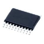
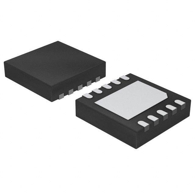
| 供应商器件封装 | 20-HTSSOP |
| 其它名称 | 296-2673-5 |
| 包装 | 管件 |
| 单位重量 | 81.800 mg |
| 参考电压 | 1.1834 V |
| 商标 | Texas Instruments |
| 安装类型 | 表面贴装 |
| 安装风格 | SMD/SMT |
| 封装 | Tube |
| 封装/外壳 | 20-TSSOP(0.173",4.40mm 宽)裸焊盘 |
| 封装/箱体 | HTSSOP-20 |
| 工作温度 | -40°C ~ 125°C |
| 工厂包装数量 | 70 |
| 最大功率耗散 | 7.2 W |
| 最大工作温度 | + 125 C |
| 最大输入电压 | 5.5 V |
| 最小工作温度 | - 40 C |
| 最小输入电压 | + 2.7 V |
| 标准包装 | 70 |
| 电压-跌落(典型值) | 0.16V @ 1.5A |
| 电压-输入 | 2.7 V ~ 5.5 V |
| 电压-输出 | 1.5 V ~ 5 V |
| 电压调节准确度 | 2 % |
| 电流-输出 | 1.5A |
| 电流-限制(最小值) | - |
| 稳压器拓扑 | 正,可调式 |
| 稳压器数 | 1 |
| 系列 | TPS75101 |
| 线路调整率 | 0.01 % / V |
| 负载调节 | 1 mV |
| 输入偏压电流—最大 | 0.075 mA |
| 输出电压 | 1.5 V to 5 V |
| 输出电流 | 1.5 A |
| 输出端数量 | 1 Output |
| 输出类型 | Adjustable |


- 商务部:美国ITC正式对集成电路等产品启动337调查
- 曝三星4nm工艺存在良率问题 高通将骁龙8 Gen1或转产台积电
- 太阳诱电将投资9.5亿元在常州建新厂生产MLCC 预计2023年完工
- 英特尔发布欧洲新工厂建设计划 深化IDM 2.0 战略
- 台积电先进制程称霸业界 有大客户加持明年业绩稳了
- 达到5530亿美元!SIA预计今年全球半导体销售额将创下新高
- 英特尔拟将自动驾驶子公司Mobileye上市 估值或超500亿美元
- 三星加码芯片和SET,合并消费电子和移动部门,撤换高东真等 CEO
- 三星电子宣布重大人事变动 还合并消费电子和移动部门
- 海关总署:前11个月进口集成电路产品价值2.52万亿元 增长14.8%


PDF Datasheet 数据手册内容提取
TPS751xxQ TPS753xxQ www.ti.com SLVS241C–MARCH2000–REVISEDOCTOBER2007 TPS751xxQ with Power Good Output, TPS753xxQ with RESET Output FAST-TRANSIENT-RESPONSE 1.5-A LOW-DROPOUT VOLTAGE REGULATORS FEATURES DESCRIPTION 1 • 1.5-ALow-DropoutVoltageRegulator The TPS753xxQ and TPS751xxQ devices are 23 • Availablein1.5V,1.8V,2.5V,and3.3VFixed low-dropout regulators with integrated power-on reset OutputandAdjustableVersions and power-good (PG) functions respectively. These devices are capable of supplying 1.5 A of output • OpenDrainPower-Good(PG)StatusOutput current with a dropout of 160 mV (TPS75133Q, (TPS751xxQ) TPS75333Q). Quiescent current is 75 μA at full load • OpenDrainPower-OnResetWith100msDelay and drops down to 1 μA when the device is disabled. (TPS753xxQ) These devices are designed to have fast transient • DropoutVoltageTypically160mVat1.5A responseforlargerloadcurrentchanges. (TPS75133Q) Because the PMOS device behaves as a low-value • Ultralow75-μATypicalQuiescentCurrent resistor, the dropout voltage is very low (typically • FastTransientResponse 160 mV at an output current of 1.5 A for the TPS75x33Q) and is directly proportional to the output • 2%ToleranceOverSpecifiedConditionsfor current. Additionally, because the PMOS pass Fixed-OutputVersions element is a voltage-driven device, the quiescent • 20-PinTSSOPPowerPAD™(PWP)Package current is very low and independent of output loading • ThermalShutdownProtection (typically 75 μA over the full range of output current, 1 mA to 1.5 A). These two key specifications yield a significant improvement in operating life for APPLICATIONS battery-poweredsystems. • Telecom The device is enabled when EN is connected to a • Servers low-level input voltage. This LDO family also features • DSP,FPGASupplies a sleep mode; applying a TTL high signal to EN (enable) shuts down the regulator, reducing the quiescentcurrenttolessthan1μAatT =+25(cid:176) C. J blank blank Typical Application Circuit (Fixed Voltage Options) 3 PG or 6 VIN IN RESET PG orRESETOutput 4 7 IN SENSE 8 OUT V OUT 0.22mF 5 9 EN OUT (1) C OUT + 47mF GND 17 (1) SeeApplicationInformationforcapacitorselectiondetails. 1 Pleasebeawarethatanimportantnoticeconcerningavailability,standardwarranty,anduseincriticalapplicationsof TexasInstrumentssemiconductorproductsanddisclaimerstheretoappearsattheendofthisdatasheet. PowerPADisatrademarkofTexasInstruments. 2 Allothertrademarksarethepropertyoftheirrespectiveowners. 3 PRODUCTIONDATAinformationiscurrentasofpublicationdate. Copyright©2000–2007,TexasInstrumentsIncorporated Products conform to specifications per the terms of the Texas Instruments standard warranty. Production processing does not necessarilyincludetestingofallparameters.
TPS751xxQ TPS753xxQ www.ti.com SLVS241C–MARCH2000–REVISEDOCTOBER2007 DESCRIPTION, CONTINUED For the TPS751xxQ, the power-good terminal (PG) is an active high, open drain output for use with a power-on resetoralow-batteryindicator. The RESET (SVS, POR, or power on reset) output of the TPS753xxQ initiates a reset in microcomputer and microprocessor systems in the event of an undervoltage condition. An internal comparator in the TPS753xxQ monitors the output voltage of the regulator to detect an undervoltage condition on the regulated output voltage. When the output reaches 95% of its regulated voltage, RESET goes to a high-impedance state after a 100-ms delay. RESET goes to a logic-low state when the regulated output voltage is pulled below 95% (that is, during an overloadcondition)ofitsregulatedvoltage. The TPS751xxQ and TPS753xxQ are offered in 1.5 V, 1.8 V, 2.5 V and 3.3 V fixed-voltage versions and in an adjustable version (programmable over the range of 1.5 V to 5 V). Output voltage tolerance is specified as a maximum of 2% over line, load, and temperature ranges. The TPS751xxQ and TPS753xxQ families are availableina20-pinTSSOP(PWP)package. blank This integrated circuit can be damaged by ESD. Texas Instruments recommends that all integrated circuits be handled with appropriateprecautions.Failuretoobserveproperhandlingandinstallationprocedurescancausedamage. ESDdamagecanrangefromsubtleperformancedegradationtocompletedevicefailure.Precisionintegratedcircuitsmaybemore susceptibletodamagebecauseverysmallparametricchangescouldcausethedevicenottomeetitspublishedspecifications. ORDERINGINFORMATION(1) PRODUCT V (2) OUT TPS751xxyyyz,TPS753xxyyyz XXisnominaloutputvoltage(forexample,15=1.5V,01=Adjustable(3)). YYYispackagedesignator. Zispackagequantity. (1) ForthemostcurrentpackageandorderinginformationseethePackageOptionAddendumattheendofthisdocument,orseetheTI websiteatwww.ti.com. (2) Customfixedoutputvoltagesareavailable;minimumorderquantitiesmayapply.Contactfactoryfordetailsandavailability. (3) TheTPS75x01isprogrammableusinganexternalresistordivider(seeApplicationInformation). ABSOLUTE MAXIMUM RATINGS(1) Overoperatingtemperaturerange(unlessotherwisenoted). PARAMETER TPS751xxQ,TPS753xxQ UNIT Inputvoltagerange,V (2) –0.3to+6 V IN VoltagerangeatEN –0.3to+16.5 V MaximumPGvoltage(TPS751xxQ) 16.5 V MaximumRESETvoltage(TPS753xxQ) 16.5 V Peakoutputcurrent Internallylimited Continuoustotalpowerdissipation SeeDissipationRatingsTable OutputvoltagerangeatOUT,FB 5.5 V Operatingvirtualjunctiontemperaturerange,T –40to+125 (cid:176) C J Storagejunctiontemperaturerange,T –65to+150 (cid:176) C STG ESDrating,HBM 2 kV (1) Stressesabovetheseratingsmaycausepermanentdamagetothedevice.Exposuretoabsolutemaximumconditionsforextended periodsmaydegradedevicereliability.Thesearestressratingsonly,andfunctionaloperationofthedeviceattheseoranyother conditionsbeyondthosespecifiedisnotimplied. (2) Allvoltagesarewithrespecttonetworkterminalground. 2 SubmitDocumentationFeedback Copyright©2000–2007,TexasInstrumentsIncorporated
TPS751xxQ TPS753xxQ www.ti.com SLVS241C–MARCH2000–REVISEDOCTOBER2007 DISSIPATION RATINGS AIRFLOW DERATINGFACTOR BOARD PACKAGE (CFM) T <+25(cid:176) C ABOVET =+25(cid:176) C T =+70(cid:176) C T =+85(cid:176) C A A A A 0 2.9mW 23.5mW/(cid:176) C 1.9W 1.5W Low-K(1) PWP 300 4.3mW 34.6mW/(cid:176) C 2.8W 2.2W 0 3W 23.8mW/(cid:176) C 1.9W 1.5W High-K(2) PWP 300 7.2W 57.9mW/(cid:176) C 4.6W 3.8W (1) Thisparameterismeasuredwiththerecommendedcopperheatsinkpatternona1-layer,5-inנ5-inprintedcircuitboard(PCB),1-ounce copper,2-inנ2-incoverage(4in2). (2) Thisparameterismeasuredwiththerecommendedcopperheatsinkpatternona8-layer,1.5-inנ2-inPCB,1-ouncecopperwithlayers 1,2,4,5,7,and8at5%coverage(0.9in2)andlayers3and6at100%coverage(6in2).Formoreinformation,refertoTItechnicalbrief SLMA002. RECOMMENDED OPERATING CONDITIONS MIN MAX MAX V Inputvoltagerange(1) 2.7 5.5 V IN V Outputvoltagerange 1.5 5 V OUT I Outputcurrent 0 2.0 A OUT T Operatingvirtualjunctiontemperature –40 +125 (cid:176) C J (1) Tocalculatetheminimuminputvoltageforyourmaximumoutputcurrent,usethefollowingequation:V =V +V . IN(min) OUT(max) DO(maxload) Copyright©2000–2007,TexasInstrumentsIncorporated SubmitDocumentationFeedback 3
TPS751xxQ TPS753xxQ www.ti.com SLVS241C–MARCH2000–REVISEDOCTOBER2007 ELECTRICAL CHARACTERISTICS Overrecommendedoperatingtemperaturerange(T =–40(cid:176) Cto+125(cid:176) C),V =V +1 V;I =1 mA,V =0 V, J IN OUT(TYP) OUT EN C =47 μF,unlessotherwisenoted.TypicalvaluesareatT =+25(cid:176) C. OUT J TPS751xxQ,TPS753xxQ PARAMETER TESTCONDITIONS MIN TYP MAX UNIT Adjustableoutput 1.5V≤V ≤5.5V 0.98V 1.02V OUT OUT OUT 1.5Voutput 2.7V<V <5.5V 1.470 1.5 1.530 IN V (1) 1.8Voutput 2.8V<V <5.5V 1.764 1.8 1.836 V OUT IN 2.5Voutput 3.5V<V <5.5V 2.450 2.5 2.550 IN 3.3Voutput 4.3V<V <5.5V 3.234 3.3 3.336 IN I (2) Groundpincurrent I =1mAto1.5A 75 125 μA GND OUT ΔV %/ V OU(1T),(2) Outputvoltagelineregulation VOUT+1V<VIN≤5V 0.01 0.1 %/V OUT ΔV %/ΔI Loadregulation I =1mAto1.5A 1 mV OUT OUT OUT Outputnoise voltage V V =1.5V,C =100μF 60 μV N BW=300Hzto50 OUT OUT RMS kHz TPS75133Q V Dropoutvoltage(3) I =1.5A,V =3.2V 160 300 mV DO OUT IN TPS75333Q I Outputcurrentlimit V =0V 3.3 4.5 A CL OUT T Shutdown +150 (cid:176) C SD temperature I Standbycurrent EN=V 1 10 μA STBY IN I FBinputcurrent TPS75x01Q FB=1.5V –1 1 μA FB V High-levelenableinputvoltage 2 V EN(HI) V Low-levelenableinputvoltage 0.7 V EN(LO) PSRR Power-supplyripplerejection(2) fI=10=01H.5z,AC,OSUeTe=(11)00μF, 63 dB OUT MinimuminputvoltageforvalidPG I =300μA 1 1.3 V OUT(PG) Tripthresholdvoltage V decreasing 80 86 %V OUT OUT PG Hysteresisvoltage MeasuredatV 0.5 %V (TPS751xxQ) OUT OUT Outputlowvoltage V =2.7V,I =1mA 0.15 0.4 V IN OUT(PG) Leakagecurrent V =5.5V 1 μA (PG) Minimuminputvoltageforvalid I =300μA, OUT(RESET) 1.1 1.3 V RESET V ≤0.8V (RESET) Tripthresholdvoltage V decreasing 92 98 %V OUT OUT RESET Hysteresisvoltage MeasuredatV 0.5 %V OUT OUT (TPS753xxQ) Outputlowvoltage I =1mA 0.15 0.4 V OUT(RESET) Leakagecurrent V =5.5V 1 μA (RESET) RESETtimeoutdelay 100 ms EN=0V –1 0 1 Inputcurrent(EN) μA EN=V –1 1 IN (1) MinimumV =(V +1V)or2.7V,whicheverisgreater.MaximumV =5.5V. IN OUT IN (2) IfV ≤1.8V,thenV =2.7V,V =5.5V: OUT IN(min) IN(max) V (V -2.7V) Line Regulation (mV) = (%/V)´ OUT IN(Max) ´1000 100 IfV ≥2.5V,thenV =V +1V,V =5.5V: OUT IN(min) OUT IN(max) V [V -(V + 1V)] Line Regulation (mV) = (%/V)´ OUT IN(Max) OUT ´1000 100 (3) InputvoltageequalsV –100mV;TPS75x33Qinputvoltagemustdropto3.2Vforthistest. OUT(Typ) 4 SubmitDocumentationFeedback Copyright©2000–2007,TexasInstrumentsIncorporated
TPS751xxQ TPS753xxQ www.ti.com SLVS241C–MARCH2000–REVISEDOCTOBER2007 FUNCTIONAL BLOCK DIAGRAMS AdjustableVoltageVersions IN EN PG orRESET _ + OUT + 100ms Delay R1 _ (forRESETOption) V = 1.1834 V ref FB R2 GND External to the device Fixed-VoltageVersions IN EN PG orRESET _ + OUT SENSE + 100ms Delay R1 _ (forRESETOption) V =1.1834 V ref R2 GND Copyright©2000–2007,TexasInstrumentsIncorporated SubmitDocumentationFeedback 5
TPS751xxQ TPS753xxQ www.ti.com SLVS241C–MARCH2000–REVISEDOCTOBER2007 PIN CONFIGURATIONS TSSOP-20 PWP (TOPVIEW) GND/HEATSINK 1 20 GND/HEATSINK NC 2 19 NC IN 3 18 NC IN 4 17 GND EN 5 16 NC PG orRESET 6 15 NC FB/SENSE 7 14 NC OUTPUT 8 13 NC OUTPUT 9 12 NC GND/HEATSINK 10 11 GND/HEATSINK Table1. PINDESCRIPTIONS TPS751xxQ,TPS753xxQ TSSOP-20(PWP) NAME PINNO. I/O DESCRIPTION EN 5 I Negativepolarityenable(EN)input Adjustablevoltageversiononly;feedbackvoltageforsettingoutputvoltageof FB/SENSE 7 I thedevice.Notinternallyconnectedonadjustableversions.Senseinputfor fixedoptions. GND 17 Ground GND/HEATSINK 1,10,11,20 Ground/heatsink IN 3,4 I Inputvoltage 2,12,13,14, NC Notconnected 15,16,18,19 OUTPUT 8,9 O Regulatedoutputvoltage TPS751xxQdevicesonly;open-drainpower-good(PG)output. PG/RESET 6 O TPS753xxQdevicesonly;open-drainRESEToutput. 6 SubmitDocumentationFeedback Copyright©2000–2007,TexasInstrumentsIncorporated
TPS751xxQ TPS753xxQ www.ti.com SLVS241C–MARCH2000–REVISEDOCTOBER2007 TPS753xxQRESETTimingDiagram V IN (1) Vres Vres t VOUT VIT+(2) VIT+(2) Threshold Voltage Less than 5% of the V (2) Output Voltage V (2) IT- IT- t RESET Output 100 ms 100 ms Delay Delay Output Output Undefined Undefined t (1) V is the minimum input voltage for a valid RESET. The symbol V is not currently listed within EIA or JEDEC res res standardsforsemiconductorsymbology. (2) V :Tripvoltageistypically5%lowerthantheoutputvoltage(95%V ).V toV isthehysteresisvoltage. IT OUT IT– IT+ TPS751xxQPowerGoodTimingDiagram V IN (1) V V PG PG t VOUT VIT+(2) VIT+(2) Threshold Voltage (2) (2) V V IT- IT- t PG Output Output Output Undefined Undefined t (1) V istheminimuminputvoltageforavalidPowerGood.ThesymbolV isnotcurrentlylistedwithinEIAorJEDEC PG PG standardsforsemiconductorsymbology. (2) V :Tripvoltageistypically17%lowerthantheoutputvoltage(83%V ).V toV isthehysteresisvoltage. IT OUT IT– IT+ Copyright©2000–2007,TexasInstrumentsIncorporated SubmitDocumentationFeedback 7
TPS751xxQ TPS753xxQ www.ti.com SLVS241C–MARCH2000–REVISEDOCTOBER2007 TYPICAL CHARACTERISTICS TableofGraphs FIGURENO. vsOutputCurrent Figure3,Figure4 V OutputVoltage vsJunctionTemperature Figure5,Figure6 OUT vsTime Figure18 I GroundCurrent vsJunctionTemperature Figure7 GND PSRR Power-SupplyRippleRejection vsFrequency Figure8 OutputSpectralNoiseDensity vsFrequency Figure9 Z OutputImpedance vsFrequency Figure10 OUT vsInputVoltage Figure11 V DropoutVoltage DO vsJunctionTemperature Figure12 V InputVoltage(Min) vsOutputVoltage Figure13 IN LINE LineTransientResponse Figure14,Figure16 LOAD LoadTransientResponse Figure15,Figure17 ESR EquivalentSeriesResistance vsOutputCurrent Figure20,Figure21 8 SubmitDocumentationFeedback Copyright©2000–2007,TexasInstrumentsIncorporated
TPS751xxQ TPS753xxQ www.ti.com SLVS241C–MARCH2000–REVISEDOCTOBER2007 TYPICAL CHARACTERISTICS Overoperatingtemperaturerange(T=–40(cid:176) Cto+125(cid:176) C)unlessotherwisenoted.TypicalvaluesareatT =+25(cid:176) C. J J TPS75x33Q TPS75x15Q OUTPUTVOLTAGE OUTPUTVOLTAGE vsOUTPUTCURRENT vsOUTPUTCURRENT 3.305 1.503 VIN= 4.3 V VIN= 2.7 V TJ= +25°C TJ= +25°C 1.502 3.303 V OUT -V VOUT -V 1.501 Output Voltage 33..239091 Output Voltage 1.5 - - VOUT VOUT 1.499 3.297 1.498 3.295 1.497 0 500 1000 1500 0 500 1000 1500 IOUT-Output Current-mA IOUT-Output Current-mA Figure3. Figure4. TPS75x33Q TPS75x15Q OUTPUTVOLTAGE OUTPUTVOLTAGE vsJUNCTIONTEMPERATURE vsJUNCTIONTEMPERATURE 3.37 1.53 VIN= 4.3 V VIN= 2.7 V 3.35 1.52 1mA V 3.33 V -e 1mA -e 1.51 g g a a olt 3.31 olt V V ut ut 1.50 p p Out 3.29 Out 1.5A -UT 1.5A -UT 1.49 VO 3.27 VO 1.48 3.25 3.23 1.47 -40 10 60 110 160 -40 10 60 110 160 T -Junction Temperature-°C T -Junction Temperature-°C J J Figure5. Figure6. Copyright©2000–2007,TexasInstrumentsIncorporated SubmitDocumentationFeedback 9
TPS751xxQ TPS753xxQ www.ti.com SLVS241C–MARCH2000–REVISEDOCTOBER2007 TYPICAL CHARACTERISTICS (continued) Overoperatingtemperaturerange(T=–40(cid:176) Cto+125(cid:176) C)unlessotherwisenoted.TypicalvaluesareatT =+25(cid:176) C. J J TPS75xxxQ TPS75x33Q GROUNDCURRENT POWER-SUPPLYRIPPLEREJECTION vsJUNCTIONTEMPERATURE vsFREQUENCY 90 100 V = 5 V IN I = 1.5 A OUT 90 85 B d V = 4.3 V - 80 IN o C = 100mF 80 Rati 70 IOOUUTT=1 mA A n T = +25°C -murrent 7705 y Rejectio 6500 J C pl d p un Su 40 Gro 65 wer- VIN= 4.3 V o 30 C = 100mF P OUT 60 - IOUT=1.5 A RR 20 TJ= +25°C S 55 P 10 50 0 -40 10 60 110 160 10 100 1k 10k 100k 1M 10M T -Junction Temperature-°C f-Frequency-Hz J Figure7. Figure8. TPS75x33Q TPS75x33Q OUTPUTSPECTRALNOISEDENSITY OUTPUTIMPEDANCE vsFREQUENCY vsFREQUENCY 2.0 1 10 V = 4.3 V 1.8 IN V = 3.3 V OUT C = 100mF C = 100mF OUT 1.6 OUT I = 1 mA T = +25°C OUT J z W ÖH 1.4 - nV/ nce 1 -oltage Noise 101...082 IOUT= 1.5 A Output Impeda -VVn 0.6 -OUT 10-1 CI OUT== 1 1.50 0AmF Z OUT 0.4 0.2 I = 1 mA OUT 0 -2 10 10 100 1k 10k 50k 10 100 1k 10k 100k 1M 10M f-Frequency-Hz f-Frequency-Hz Figure9. Figure10. 10 SubmitDocumentationFeedback Copyright©2000–2007,TexasInstrumentsIncorporated
TPS751xxQ TPS753xxQ www.ti.com SLVS241C–MARCH2000–REVISEDOCTOBER2007 TYPICAL CHARACTERISTICS (continued) Overoperatingtemperaturerange(T=–40(cid:176) Cto+125(cid:176) C)unlessotherwisenoted.TypicalvaluesareatT =+25(cid:176) C. J J TPS75x01Q TPS75x33Q DROPOUTVOLTAGE DROPOUTVOLTAGE vsINPUTVOLTAGE vsJUNCTIONTEMPERATURE 300 300 I = 1.5 A OUT 250 250 V V m m - 200 TJ= +125°C - 200 ge ge IOUT= 1.5 A a a olt olt V V ut 150 TJ= +25°C ut 150 o o p p o o Dr Dr - 100 TJ=-40°C - 100 O O D D V V I = 0.5 A OUT 50 50 0 0 2.5 3 3.5 4 4.5 5 -40 10 60 110 160 VIN-Input Voltage-V TJ-Junction Temperature-°C Figure11. Figure12. INPUTVOLTAGE(MIN) TPS75x15Q vsOUTPUTVOLTAGE LINETRANSIENTRESPONSE 4.0 -n)V IOUT= 1.5 A TA= +25°C -Change inUT-ut VoltagemV 100 ICVOOOUUUTTT=== 1 11.5.05 0A VmF ddVT =1m sV e (Mi TA= +125°C DVOOutp 0 g olta 3.0 -100 V Input 2.7 TA=-40°C -geV - a VIN Volt 4 ut p n I - 3 N VI 2.0 1.5 1.75 2 2.25 2.5 2.75 3 3.25 3.5 0 0.1 0.2 0.3 0.4 0.5 0.6 0.7 0.8 0.9 1.0 VOUT-Output Voltage-V t-Time-ms Figure13. Figure14. Copyright©2000–2007,TexasInstrumentsIncorporated SubmitDocumentationFeedback 11
TPS751xxQ TPS753xxQ www.ti.com SLVS241C–MARCH2000–REVISEDOCTOBER2007 TYPICAL CHARACTERISTICS (continued) Overoperatingtemperaturerange(T=–40(cid:176) Cto+125(cid:176) C)unlessotherwisenoted.TypicalvaluesareatT =+25(cid:176) C. J J TPS75x15Q TPS75x33Q LOADTRANSIENTRESPONSE LINETRANSIENTRESPONSE Change in-oltagemV 500 ICVLOOLOUAATDD=== 11 1..550 0VAmF (Tantalum) Change in-oltagemV 100 ICVOOOUUUTTT=== 1 31.5.03 0A VmF (Tantalum) ddVT =1m sV - V - V UTut UTut DVOOutp -50 DVOOutp 0 -100 -100 A - V Current -150 -oltage put 1.5 ut V 5.3 Out Inp - - 4.3 UT VIN O I 0 0 1 2 3 4 5 6 7 8 9 10 0 0.1 0.2 0.3 0.4 0.5 0.6 0.7 0.8 0.9 1.0 t-Time-ms t-Time-ms Figure15. Figure16. TPS75x33Q TPS75x33QOUTPUTVOLTAGE LOADTRANSIENTRESPONSE vsTIME(ATSTARTUP) V ILOAD= 1.5 A - VIN= 4.3 V Change in-oltagemV 500 CVOLOUATD== 3 1.30 0VmF (Tantalum) put Voltage 3.3 TJ= +25°C -UTut V Out DVOOutp -50 -OUT V -100 0 A - V nt -150 - 4.3 e e put Curr 1.5 e Voltag 0 ut bl O na - E T U O I 0 0 0.2 0.4 0.6 0.8 1.0 0 1 2 3 4 5 6 7 8 9 10 t-Time-ms t-Time-ms Figure17. Figure18. 12 SubmitDocumentationFeedback Copyright©2000–2007,TexasInstrumentsIncorporated
TPS751xxQ TPS753xxQ www.ti.com SLVS241C–MARCH2000–REVISEDOCTOBER2007 TYPICAL CHARACTERISTICS (continued) Overoperatingtemperaturerange(T=–40(cid:176) Cto+125(cid:176) C)unlessotherwisenoted.TypicalvaluesareatT =+25(cid:176) C. J J TestCircuitforTypicalRegionsofStability(Figure20andFigure21)(FixedOutputOptions) VIN IN To Load OUT + C OUT EN R GND L ESR Figure19. TYPICALREGIONOFSTABILITY TYPICALREGIONOFSTABILITY EQUIVALENTSERIESRESISTANCE(1) EQUIVALENTSERIESRESISTANCE(1) vsOUTPUTCURRENT vsOUTPUTCURRENT 10 10 V = 3.3 V V = 3.3 V OUT OUT C = 100mF C = 47mF OUT OUT V =4.3 V V =4.3 V W TIN= +25°C W TIN= +25°C - J - J e e c c n n a a st 1 st 1 si si e e R RegionofStability R RegionofStability s s e e eri eri S S nt nt e e al al v v ui 0.1 ui 0.1 q q E E - - R 0.05 R S S E E RegionofInstability RegionofInstability 0.01 0.01 0 0.5 1.0 1.5 0 0.5 1.0 1.5 I -Output Current-A I -Output Current-A OUT OUT Figure20. Figure21. (1). Equivalent series resistance (ESR) refers to the total series resistance, including the ESR of the capacitor, anyseriesresistanceaddedexternally,andPWBtraceresistancetoC . OUT Copyright©2000–2007,TexasInstrumentsIncorporated SubmitDocumentationFeedback 13
TPS751xxQ TPS753xxQ www.ti.com SLVS241C–MARCH2000–REVISEDOCTOBER2007 APPLICATION INFORMATION The TPS751xxQ and TPS753xxQ devices include four fixed-output voltage regulators (1.5 V, 1.8 V, 2.5 V and 3.3V),andanadjustableregulator,theTPS75x01Q(adjustablefrom1.5Vto5V). Minimum Load Requirements The TPS751xxQ and TPS753xxQ families are stable even at zero load; no minimum load is required for operation. Pin Functions Enable(EN) The EN terminal is an input that enables or shuts down the device. If EN is a logic high, the device is in shutdownmode.WhenENgoestologiclow,thenthedeviceisenabled. Power-Good(PG)—TPS751xxQ The PG terminal is an open drain, active high output that indicates the status of V (output of the LDO). When OUT V reaches 83% of the regulated voltage, PG goes to a high impedance state. It goes to a low-impedance OUT state when V falls below 83% (that is, an overload condition) of the regulated voltage. The open drain output OUT ofthePGterminalrequiresapullupresistor. Sense(SENSE) The SENSE terminal of the fixed output options must be connected to the regulator output, and the connection should be as short as possible. Internally, SENSE connects to a high-impedance wide-bandwidth amplifier through a resistor-divider network, and noise pickup feeds through to the regulator output. It is essential to route the SENSE connection in such a way to minimize/avoid noise pickup. Adding RC networks between the SENSE terminal and V to filter noise is not recommended because these types of networks may cause the regulator OUT tooscillate. Reset(RESET)—TPS753xxQ The RESET terminal is an open drain, active low output that indicates the status of V . When V reaches OUT OUT 95% of the regulated voltage, RESET goes to a high-impedance state after a 100-ms delay. RESET goes to a low-impedance state when V is below 95% of the regulated voltage. The open-drain output of the RESET OUT terminalrequiresapullupresistor. GND/HEATSINK All GND/HEATSINK terminals are connected directly to the mount pad for thermal-enhanced operation. These terminalscouldbeconnectedtoGNDorleftfloating. InputCapacitor For a typical application, an input bypass capacitor (0.22 μF to 1 μF) is recommended for device stability. This capacitor should be as close to the input pins as possible. For fast transient conditions where droop at the input of the LDO may occur because of high inrush current, it is recommended to place a larger capacitor at the input aswell.Thesizeofthis capacitor depends on the output current and response time of the main power supply, as wellasthedistancetotheload(LDO). OutputCapacitor As with most LDO regulators, the TPS751xxQ and TPS753xxQ require an output capacitor connected between OUT and GND to stabilize the internal control loop. The minimum recommended capacitance value is 47 μF and theESR (equivalent series resistance) must be between 100 mΩ and 10 Ω. Solid tantalum electrolytic, aluminum electrolytic, and multilayer ceramic capacitors are all suitable, provided they meet the requirements described in thissection.Largercapacitorsprovideawiderrangeofstabilityandbetterloadtransientresponse. 14 SubmitDocumentationFeedback Copyright©2000–2007,TexasInstrumentsIncorporated
TPS751xxQ TPS753xxQ www.ti.com SLVS241C–MARCH2000–REVISEDOCTOBER2007 This information, along with the ESR graphs (see Figure 20 and Figure 21), is included to assist in selection of suitable capacitance for the user’s application. When necessary to achieve low height requirements along with high output current and/or high load capacitance, several higher ESR capacitors can be used in parallel to meet theseguidelines. ESR and Transient Response LDOs typically require an external output capacitor for stability. In fast transient response applications, capacitors are used to support the load current while the LDO amplifier is responding. In most applications, one capacitor is usedtosupportbothfunctions. Besides its capacitance, every capacitor also contains parasitic impedances. These parasitic impedances are resistive as well as inductive. The resistive impedance is called equivalent series resistance (ESR), and the inductive impedance is called equivalent series inductance (ESL). The equivalent schematic diagram of any capacitorcanthereforebedrawnasshowninFigure22. R L ESR ESL C Figure22.ESRandESL In most cases one can neglect the effect of inductive impedance ESL. Therefore, the following application focusesmainlyontheparasiticresistanceESR.. Figure23showstheoutputcapacitoranditsparasiticimpedancesinatypicalLDOoutputstage. I OUT LDO + V R ESR ESR – V V IN R OUT LOAD C OUT Figure23.LDOOutputStageWithParasiticResistancesESRandESL Copyright©2000–2007,TexasInstrumentsIncorporated SubmitDocumentationFeedback 15
TPS751xxQ TPS753xxQ www.ti.com SLVS241C–MARCH2000–REVISEDOCTOBER2007 In steady state operation (dc state condition), the load current is supplied by the LDO (solid arrow) and the voltage across the capacitor is the same as the output voltage (V(C ) = V ). This condition means that no OUT OUT current is flowing into the C branch. If I suddenly increases (that is, a transient condition), the following OUT OUT eventsoccur: • The LDO is not able to supply the sudden current need because of its response time (t in Figure 24). 1 Therefore, capacitor C provides the current for the new load condition (the dashed arrow). C now acts OUT OUT like a battery with an internal resistance, ESR. Depending on the current demand at the output, a voltage dropoccursatR .ThisvoltageisshownasV inFigure23. ESR ESR • When C is conducting current to the load, initial voltage at the load is V = V(C ) – V . As a result OUT OUT OUT ESR of the discharge of C , the output voltage V drops continuously until the response time t of the LDO is OUT OUT 1 reached and the LDO resumes supplying the load. From this point, the output voltage starts rising again until itreachestheregulatedvoltage.Thisperiodisshownast inFigure24. 2 Figure 24 also shows the impact of different ESRs on the output voltage. The left brackets show different levels ofESRswherenumber1displaysthelowestandnumber3displaysthehighestESR. Fromtheabovediscussion,thefollowingconclusionscanbedrawn: • ThehighertheESR,thelargerthedroopatthebeginningofloadtransient. • The smaller the output capacitor, the faster the discharge time and the bigger the voltage droop during the LDOresponseperiod. Conclusion To minimize the transient output droop, capacitors must have a low ESR and be large enough to support the minimumoutputvoltagerequirement. I OUT V OUT 1 2 3 ESR1 ESR2 ESR3 t t 1 2 Figure24.CorrelationofDifferentESRsandTheirInfluencetotheRegulationofV ataLoadStep OUT FromLow-to-HighOutputCurrent 16 SubmitDocumentationFeedback Copyright©2000–2007,TexasInstrumentsIncorporated
TPS751xxQ TPS753xxQ www.ti.com SLVS241C–MARCH2000–REVISEDOCTOBER2007 Programming the TPS75x01Q Adjustable LDO Regulator The output voltage of the TPS77x01Q adjustable regulator is programmed using an external resistor divider as showninFigure25.TheoutputvoltageiscalculatedusingEquation1: R V = V ´(1 + 1 ) OUT ref R 2 (1) Where: • V =1.1834Vtyp(theinternalreferencevoltage) ref Resistors R and R should be chosen for approximately 40μA divider current. Lower value resistors can be 1 2 used, but offer no inherent advantage and waste more power. Higher values should be avoided as leakage currents at FB increase the output voltage error. The recommended design procedure is to choose R = 30.1 kΩ 2 tosetthedividercurrentatapproximately40μAandthencalculateR usingEquation2: 1 V R = ( OUT -1)´R 1 V 2 ref (2) TPS75x01Q OUTPUT VOLTAGE PROGRAMMING GUIDE V IN PG/ PG orRESETOutput OUTPUT IN RESET VOLTAGE R R UNIT 0.22mF 1 2 250 kW 2.5 V 33.2 30.1 kW OUT V 3.3 V 53.6 30.1 kW OUT >2.0 V 3.6 V 61.9 30.1 kW EN R1 <0.7 V NOTE: To reduce noise and prevent oscillation, FB/SENSE COUT R1and R2must be as close as possible to the GND FB/SENSE terminal. R 2 Figure25.TPS75x01QAdjustableLDORegulatorProgramming Regulator Protection The TPS751xxQ and TPS753xxQ PMOS-pass transistors have a built-in back diode that conducts reverse currents when the input voltage drops below the output voltage (for example, during power down). Current is conductedfromtheoutputtotheinputandisnotinternallylimited.When extended reverse voltage is anticipated, externallimitingmaybeappropriate. The TPS751xxQ and TPS753xxQ also feature internal current limiting and thermal protection. During normal operation, the TPS751xxQ and TPS753xxQ limit output current to approximately 3.3 A. When current limiting engages, the output voltage scales back linearly until the overcurrent condition ends. While current limiting is designed to prevent gross device failure, care should be taken not to exceed the power dissipation ratings of the package. If the temperature of the device exceeds +150(cid:176) C (typ), thermal-protection circuitry shuts it down. Once thedevicehascooledbelow+130(cid:176) C(typ),regulatoroperationresumes. Copyright©2000–2007,TexasInstrumentsIncorporated SubmitDocumentationFeedback 17
TPS751xxQ TPS753xxQ www.ti.com SLVS241C–MARCH2000–REVISEDOCTOBER2007 Power Dissipation and Junction Temperature Specified regulator operation is assured to a junction temperature of +125(cid:176) C; the maximum junction temperature should be restricted to +125(cid:176) C under normal operating conditions. This restriction limits the power dissipation the regulator can handle in any given application. To ensure the junction temperature is within acceptable limits, calculate the maximum allowable dissipation, P , and the actual dissipation, P , which must be less than or D(max) D equaltoP . D(max) Themaximum-power-dissipationlimitisdeterminedusingEquation3: T -T P = J(Max) A D(Max) R qJA (3) where: • T isthemaximumallowablejunctiontemperature J(max) • R isthethermalresistancejunction-to-ambientforthepackage;thatis,34.6(cid:176) C/Wforthe20-terminalPWP θJA withnoairflow(seeDissipationRatingsTable). • T istheambienttemperature A TheregulatordissipationiscalculatedusingEquation4: P = (V -V )´I D IN OUT OUT (4) Power dissipation resulting from quiescent current is negligible. Excessive power dissipation triggers the thermal protectioncircuit. THERMAL INFORMATION Thermally-EnhancedTSSOP-20(PWP–PowerPAD) The thermally-enhanced PWP package is based on the 20-pin TSSOP, but includes a thermal pad [see Figure26(c)]toprovideaneffectivethermalcontactbetweentheICandtheprintedwiringboard(PWB). DIE (a)SideView Thermal Pad DIE (b)EndView (c)BottomView Figure26.ViewsofThermally-EnhancedPWPPackage Traditionally, surface mount and power have been mutually exclusive terms. A variety of scaled-down TO220-type packages have leads formed as gull wings to make them applicable for surface-mount applications. These packages, however, suffer from several shortcomings: they do not address the very low profile requirements (less than 2 mm) of many of today’s advanced systems, and they do not offer a pin-count high enough to accommodate increasing integration. On the other hand, traditional low-power surface-mount packages require power dissipation derating that severely limits the usable range of many high-performance analogcircuits. The PWP package (a thermally-enhanced TSSOP) combines fine-pitch surface-mount technology with thermal performancecomparabletomuchlargerpowerpackages. 18 SubmitDocumentationFeedback Copyright©2000–2007,TexasInstrumentsIncorporated
TPS751xxQ TPS753xxQ www.ti.com SLVS241C–MARCH2000–REVISEDOCTOBER2007 The PWP package is designed to optimize the heat transfer to the PWB. Because of the very small size and limited mass of a TSSOP package, thermal enhancement is achieved by improving the thermal conduction paths that remove heat from the component. The thermal pad is formed using a lead-frame design (patent pending) and manufacturing technique to provide the user with direct connection to the heat-generating IC. When this pad is soldered or otherwise coupled to an external heat dissipator, high power dissipation in the ultra-thin, fine-pitch, surface-mountpackagecanbereliablyachieved. Because the conduction path has been enhanced, power-dissipation capability is determined by the thermal considerationsinthePWBdesign.Forexample,simplyadding a localized copper plane (heatsink surface) that is coupled to the thermal pad enables the PWP package to dissipate 2.5 W in free air (see Figure 28(a), 8 cm2 of copper heatsink and natural convection). Increasing the heatsink size increases the power dissipation range for the component. The power dissipation limit can be further improved by adding airflow to a PWB/IC assembly (see Figure 27 and Figure 28). The line drawn at 0.3 cm2 in Figure 27 and Figure 28 indicates performance at theminimumrecommendedheatsinksize,illustratedinFigure30. The thermal pad is directly connected to the substrate of the IC, which for the TPS751xxQPWP and TPS753xxQPWP series is a secondary electrical connection to device ground. The heat-sink surface that is addedtothePWPcanbea ground plane or left electrically isolated. In TO220-type surface-mount packages, the thermal connection is also the primary electrical connection for a given terminal which is not always ground. The PWP package provides up to 16 independent leads that can be used as inputs and outputs. (Note: leads 1, 10, 11,and20areinternallyconnectedtothethermalpadandtheICsubstrate.) 150 NaturalConvection 50ft/min W C/ ° 100ft/min - e nc 100 150 ft/min a st si e 200 ft/min R al m er 75 h T - A RqJ 50 250ft/min 300 ft/min 25 0 0.3 1 2 3 4 5 6 7 8 Copper Heatsink Area-cm2 Figure27.ThermalResistancevsCopperHeatsinkArea Copyright©2000–2007,TexasInstrumentsIncorporated SubmitDocumentationFeedback 19
TPS751xxQ TPS753xxQ www.ti.com SLVS241C–MARCH2000–REVISEDOCTOBER2007 3.5 3.5 T = +25°C T = +55°C A A 300ft/min 3.0 3.0 W 150 ft/min W -mit 2.5 -mit 2.5 300ft/min Li Li n n atio 2.0 atio 2.0 150ft/min p NaturalConvection p si si s s Di 1.5 Di 1.5 er er NaturalConvection w w o o -P 1.0 -P 1.0 D D P P 0.5 0.5 0 0 00.3 2 4 6 8 00.3 2 4 6 8 Copper Heatsink Area-cm2 Copper Heatsink Area-cm2 (a) (b) 3.5 T = +105°C A 3.0 W -mit 2.5 Li n atio 2.0 p si s Di 1.5 er 150 ft/min w o 300ft/min P - 1.0 D P NaturalConvection 0.5 0 00.3 2 4 6 8 Copper Heatsink Area-cm2 (c) Figure28.PowerRatingsofthePWPPackageatAmbientTemperaturesof+25(cid:176) C,+55(cid:176) C,and+105(cid:176) C 20 SubmitDocumentationFeedback Copyright©2000–2007,TexasInstrumentsIncorporated
TPS751xxQ TPS753xxQ www.ti.com SLVS241C–MARCH2000–REVISEDOCTOBER2007 Figure 29 is an example of a thermally-enhanced PWB layout for use with the new PWP package. This board configuration was used in the thermal experiments that generated the power ratings shown in Figure 27 and Figure 28. As discussed earlier, copper has been added on the PWB to conduct heat away from the device. R θJA for this assembly is illustrated in Figure 27 as a function of heatsink area. A family of curves is included to illustratetheeffectofairflowintroducedintothesystem. HeatsinkArea 1 oz Copper Boardthickness 62mils (0.15748 cm) Board size 3.2 in. x 3.2 in. Board material FR4 Copper trace/heatsink 1oz Exposed pad mounting 63/67 tin/lead (Sn/Pb) solder Figure29.PWBLayout(IncludingCopperHeatsinkArea)forThermally-EnhancedPWPPackage From Figure 27, R for a PWB assembly can be determined and used to calculate the maximum θJA power-dissipationlimitforthecomponent/PWBassembly,withtheequation: T -T P = J(Max) A D(Max) R qJA(System) (5) Where T is the maximum specified junction temperature (+150(cid:176) C absolute maximum limit, +125(cid:176) C Jmax recommendedoperatinglimit)andT istheambienttemperature. A P should then be applied to the internal power dissipated by the TPS75133QPWP regulator. The equation D(max) forcalculatingtotalinternalpowerdissipationoftheTPS75133QPWPis: P = (V -V )´I + V ´I D(total) IN OUT OUT IN Q (6) Because the quiescent current of the TPS75133QPWP is very low, the second term is negligible, further simplifyingtheequationto: P = (V -V )´I D(total) IN OUT OUT (7) For the case where T = +55(cid:176) C, airflow = 200 ft/min, copper heat-sink area = 4 cm2, the maximum A power-dissipation limit can be calculated. First, from Figure 27, we find the system R is 50(cid:176) C/W; therefore, the θJA maximumpower-dissipationlimitis: P = TJ(Max)-TA =125°C-55°C = 1.4 W D(Max) RqJA(System) 50°C/W (8) If the system implements a TPS75133QPWP regulator, where V = 5 V and I = 800 mA, the internal power IN OUT dissipationis: P = (V -V )´I = (5-3.3)´0.8 = 1.36 W D(total) IN OUT OUT (9) Comparing P with P reveals that the power dissipation in this example does not exceed the calculated D(total) D(max) limit. When it does, one of two corrective actions should be made: either raise the power-dissipation limit by increasing the airflow or the heat-sink area, or loweri the internal power dissipation of the regulator by reducing the input voltage or the load current. In either case, the above calculations should be repeated with the new systemparameters. Copyright©2000–2007,TexasInstrumentsIncorporated SubmitDocumentationFeedback 21
TPS751xxQ TPS753xxQ www.ti.com SLVS241C–MARCH2000–REVISEDOCTOBER2007 MountingInformation The primary requirement is to complete the thermal contact between the thermal pad and the PWB metal. The thermal pad is a solderable surface and is fully intended to be soldered at the time the component is mounted. Althoughvoidinginthethermal-padsolder-connectionisnotdesirable,upto50%voidingisacceptable. The data included in Figure 27 and Figure 28 are for soldered connections with voiding between 20% and 50%. The thermalanalysisshowsnosignificantdifferenceresultingfromthevariationinvoidingpercentage. Figure 30 shows the solder-mask land pattern for the PWP package. The minimum recommended heat-sink area is also illustrated. This is simply a copper plane under the body extent of the package, including metal routed underterminals1,10,11,and20. Minimum Recommended Locationof Exposed Heatsink Area Thermal Pad on PWP Package Figure30.PWPPackageLandPattern 22 SubmitDocumentationFeedback Copyright©2000–2007,TexasInstrumentsIncorporated
PACKAGE OPTION ADDENDUM www.ti.com 24-Aug-2018 PACKAGING INFORMATION Orderable Device Status Package Type Package Pins Package Eco Plan Lead/Ball Finish MSL Peak Temp Op Temp (°C) Device Marking Samples (1) Drawing Qty (2) (6) (3) (4/5) TPS75101QPWP ACTIVE HTSSOP PWP 20 70 Green (RoHS CU NIPDAU Level-2-260C-1 YEAR -40 to 125 PT75101 & no Sb/Br) TPS75101QPWPR ACTIVE HTSSOP PWP 20 2000 Green (RoHS CU NIPDAU Level-2-260C-1 YEAR -40 to 125 PT75101 & no Sb/Br) TPS75115QPWP ACTIVE HTSSOP PWP 20 70 Green (RoHS CU NIPDAU Level-2-260C-1 YEAR -40 to 125 PT75115 & no Sb/Br) TPS75115QPWPR ACTIVE HTSSOP PWP 20 2000 Green (RoHS CU NIPDAU Level-2-260C-1 YEAR -40 to 125 PT75115 & no Sb/Br) TPS75118QPWP ACTIVE HTSSOP PWP 20 70 Green (RoHS CU NIPDAU Level-2-260C-1 YEAR -40 to 125 PT75118 & no Sb/Br) TPS75118QPWPR ACTIVE HTSSOP PWP 20 2000 Green (RoHS CU NIPDAU Level-2-260C-1 YEAR -40 to 125 PT75118 & no Sb/Br) TPS75125QPWP ACTIVE HTSSOP PWP 20 70 Green (RoHS CU NIPDAU Level-2-260C-1 YEAR -40 to 125 PT75125 & no Sb/Br) TPS75125QPWPG4 ACTIVE HTSSOP PWP 20 70 Green (RoHS CU NIPDAU Level-2-260C-1 YEAR -40 to 125 PT75125 & no Sb/Br) TPS75125QPWPR ACTIVE HTSSOP PWP 20 2000 Green (RoHS CU NIPDAU Level-2-260C-1 YEAR -40 to 125 PT75125 & no Sb/Br) TPS75133QPWP ACTIVE HTSSOP PWP 20 70 Green (RoHS CU NIPDAU Level-2-260C-1 YEAR -40 to 125 PT75133 & no Sb/Br) TPS75133QPWPR ACTIVE HTSSOP PWP 20 2000 Green (RoHS CU NIPDAU Level-2-260C-1 YEAR -40 to 125 PT75133 & no Sb/Br) TPS75301QPWP ACTIVE HTSSOP PWP 20 70 Green (RoHS CU NIPDAU Level-2-260C-1 YEAR -40 to 125 PT75301 & no Sb/Br) TPS75301QPWPR ACTIVE HTSSOP PWP 20 2000 Green (RoHS CU NIPDAU Level-2-260C-1 YEAR -40 to 125 PT75301 & no Sb/Br) TPS75315QPWP ACTIVE HTSSOP PWP 20 70 Green (RoHS CU NIPDAU Level-2-260C-1 YEAR -40 to 125 PT75315 & no Sb/Br) TPS75318QPWP ACTIVE HTSSOP PWP 20 70 Green (RoHS CU NIPDAU Level-2-260C-1 YEAR -40 to 125 PT75318 & no Sb/Br) TPS75318QPWPR ACTIVE HTSSOP PWP 20 2000 Green (RoHS CU NIPDAU Level-2-260C-1 YEAR -40 to 125 PT75318 & no Sb/Br) TPS75325QPWP ACTIVE HTSSOP PWP 20 70 Green (RoHS CU NIPDAU Level-2-260C-1 YEAR -40 to 125 PT75325 & no Sb/Br) Addendum-Page 1
PACKAGE OPTION ADDENDUM www.ti.com 24-Aug-2018 Orderable Device Status Package Type Package Pins Package Eco Plan Lead/Ball Finish MSL Peak Temp Op Temp (°C) Device Marking Samples (1) Drawing Qty (2) (6) (3) (4/5) TPS75325QPWPR ACTIVE HTSSOP PWP 20 2000 Green (RoHS CU NIPDAU Level-2-260C-1 YEAR -40 to 125 PT75325 & no Sb/Br) TPS75333QPWP ACTIVE HTSSOP PWP 20 70 Green (RoHS CU NIPDAU Level-2-260C-1 YEAR -40 to 125 PT75333 & no Sb/Br) TPS75333QPWPR ACTIVE HTSSOP PWP 20 2000 Green (RoHS CU NIPDAU Level-2-260C-1 YEAR -40 to 125 PT75333 & no Sb/Br) TPS75333QPWPRG4 ACTIVE HTSSOP PWP 20 2000 Green (RoHS CU NIPDAU Level-2-260C-1 YEAR -40 to 125 PT75333 & no Sb/Br) (1) The marketing status values are defined as follows: ACTIVE: Product device recommended for new designs. LIFEBUY: TI has announced that the device will be discontinued, and a lifetime-buy period is in effect. NRND: Not recommended for new designs. Device is in production to support existing customers, but TI does not recommend using this part in a new design. PREVIEW: Device has been announced but is not in production. Samples may or may not be available. OBSOLETE: TI has discontinued the production of the device. (2) RoHS: TI defines "RoHS" to mean semiconductor products that are compliant with the current EU RoHS requirements for all 10 RoHS substances, including the requirement that RoHS substance do not exceed 0.1% by weight in homogeneous materials. Where designed to be soldered at high temperatures, "RoHS" products are suitable for use in specified lead-free processes. TI may reference these types of products as "Pb-Free". RoHS Exempt: TI defines "RoHS Exempt" to mean products that contain lead but are compliant with EU RoHS pursuant to a specific EU RoHS exemption. Green: TI defines "Green" to mean the content of Chlorine (Cl) and Bromine (Br) based flame retardants meet JS709B low halogen requirements of <=1000ppm threshold. Antimony trioxide based flame retardants must also meet the <=1000ppm threshold requirement. (3) MSL, Peak Temp. - The Moisture Sensitivity Level rating according to the JEDEC industry standard classifications, and peak solder temperature. (4) There may be additional marking, which relates to the logo, the lot trace code information, or the environmental category on the device. (5) Multiple Device Markings will be inside parentheses. Only one Device Marking contained in parentheses and separated by a "~" will appear on a device. If a line is indented then it is a continuation of the previous line and the two combined represent the entire Device Marking for that device. (6) Lead/Ball Finish - Orderable Devices may have multiple material finish options. Finish options are separated by a vertical ruled line. Lead/Ball Finish values may wrap to two lines if the finish value exceeds the maximum column width. Important Information and Disclaimer:The information provided on this page represents TI's knowledge and belief as of the date that it is provided. TI bases its knowledge and belief on information provided by third parties, and makes no representation or warranty as to the accuracy of such information. Efforts are underway to better integrate information from third parties. TI has taken and continues to take reasonable steps to provide representative and accurate information but may not have conducted destructive testing or chemical analysis on incoming materials and chemicals. TI and TI suppliers consider certain information to be proprietary, and thus CAS numbers and other limited information may not be available for release. Addendum-Page 2
PACKAGE OPTION ADDENDUM www.ti.com 24-Aug-2018 In no event shall TI's liability arising out of such information exceed the total purchase price of the TI part(s) at issue in this document sold by TI to Customer on an annual basis. Addendum-Page 3
PACKAGE MATERIALS INFORMATION www.ti.com 20-Feb-2019 TAPE AND REEL INFORMATION *Alldimensionsarenominal Device Package Package Pins SPQ Reel Reel A0 B0 K0 P1 W Pin1 Type Drawing Diameter Width (mm) (mm) (mm) (mm) (mm) Quadrant (mm) W1(mm) TPS75101QPWPR HTSSOP PWP 20 2000 330.0 16.4 6.95 7.1 1.6 8.0 16.0 Q1 TPS75115QPWPR HTSSOP PWP 20 2000 330.0 16.4 6.95 7.1 1.6 8.0 16.0 Q1 TPS75118QPWPR HTSSOP PWP 20 2000 330.0 16.4 6.95 7.1 1.6 8.0 16.0 Q1 TPS75125QPWPR HTSSOP PWP 20 2000 330.0 16.4 6.95 7.1 1.6 8.0 16.0 Q1 TPS75133QPWPR HTSSOP PWP 20 2000 330.0 16.4 6.95 7.1 1.6 8.0 16.0 Q1 TPS75301QPWPR HTSSOP PWP 20 2000 330.0 16.4 6.95 7.1 1.6 8.0 16.0 Q1 TPS75318QPWPR HTSSOP PWP 20 2000 330.0 16.4 6.95 7.1 1.6 8.0 16.0 Q1 TPS75325QPWPR HTSSOP PWP 20 2000 330.0 16.4 6.95 7.1 1.6 8.0 16.0 Q1 TPS75333QPWPR HTSSOP PWP 20 2000 330.0 16.4 6.95 7.1 1.6 8.0 16.0 Q1 PackMaterials-Page1
PACKAGE MATERIALS INFORMATION www.ti.com 20-Feb-2019 *Alldimensionsarenominal Device PackageType PackageDrawing Pins SPQ Length(mm) Width(mm) Height(mm) TPS75101QPWPR HTSSOP PWP 20 2000 350.0 350.0 43.0 TPS75115QPWPR HTSSOP PWP 20 2000 350.0 350.0 43.0 TPS75118QPWPR HTSSOP PWP 20 2000 350.0 350.0 43.0 TPS75125QPWPR HTSSOP PWP 20 2000 350.0 350.0 43.0 TPS75133QPWPR HTSSOP PWP 20 2000 350.0 350.0 43.0 TPS75301QPWPR HTSSOP PWP 20 2000 350.0 350.0 43.0 TPS75318QPWPR HTSSOP PWP 20 2000 350.0 350.0 43.0 TPS75325QPWPR HTSSOP PWP 20 2000 350.0 350.0 43.0 TPS75333QPWPR HTSSOP PWP 20 2000 350.0 350.0 43.0 PackMaterials-Page2
None
None
None
IMPORTANTNOTICEANDDISCLAIMER TIPROVIDESTECHNICALANDRELIABILITYDATA(INCLUDINGDATASHEETS),DESIGNRESOURCES(INCLUDINGREFERENCE DESIGNS),APPLICATIONOROTHERDESIGNADVICE,WEBTOOLS,SAFETYINFORMATION,ANDOTHERRESOURCES“ASIS” ANDWITHALLFAULTS,ANDDISCLAIMSALLWARRANTIES,EXPRESSANDIMPLIED,INCLUDINGWITHOUTLIMITATIONANY IMPLIEDWARRANTIESOFMERCHANTABILITY,FITNESSFORAPARTICULARPURPOSEORNON-INFRINGEMENTOFTHIRD PARTYINTELLECTUALPROPERTYRIGHTS. TheseresourcesareintendedforskilleddevelopersdesigningwithTIproducts.Youaresolelyresponsiblefor(1)selectingtheappropriate TIproductsforyourapplication,(2)designing,validatingandtestingyourapplication,and(3)ensuringyourapplicationmeetsapplicable standards,andanyothersafety,security,orotherrequirements.Theseresourcesaresubjecttochangewithoutnotice.TIgrantsyou permissiontousetheseresourcesonlyfordevelopmentofanapplicationthatusestheTIproductsdescribedintheresource.Other reproductionanddisplayoftheseresourcesisprohibited.NolicenseisgrantedtoanyotherTIintellectualpropertyrightortoanythird partyintellectualpropertyright.TIdisclaimsresponsibilityfor,andyouwillfullyindemnifyTIanditsrepresentativesagainst,anyclaims, damages,costs,losses,andliabilitiesarisingoutofyouruseoftheseresources. TI’sproductsareprovidedsubjecttoTI’sTermsofSale(www.ti.com/legal/termsofsale.html)orotherapplicabletermsavailableeitheron ti.comorprovidedinconjunctionwithsuchTIproducts.TI’sprovisionoftheseresourcesdoesnotexpandorotherwisealterTI’sapplicable warrantiesorwarrantydisclaimersforTIproducts. MailingAddress:TexasInstruments,PostOfficeBox655303,Dallas,Texas75265 Copyright©2019,TexasInstrumentsIncorporated