ICGOO在线商城 > 集成电路(IC) > PMIC - 稳压器 - 线性 > TPS74701DRCT
 Datasheet下载
- 型号: TPS74701DRCT
- 制造商: Texas Instruments
- 库位|库存: xxxx|xxxx
- 要求:
| 数量阶梯 | 香港交货 | 国内含税 |
| +xxxx | $xxxx | ¥xxxx |
查看当月历史价格
查看今年历史价格
TPS74701DRCT产品简介:
ICGOO电子元器件商城为您提供TPS74701DRCT由Texas Instruments设计生产,在icgoo商城现货销售,并且可以通过原厂、代理商等渠道进行代购。 TPS74701DRCT价格参考。Texas InstrumentsTPS74701DRCT封装/规格:PMIC - 稳压器 - 线性, Linear Voltage Regulator IC Positive Adjustable 1 Output 0.8 V ~ 3.6 V 500mA 10-VSON (3x3)。您可以下载TPS74701DRCT参考资料、Datasheet数据手册功能说明书,资料中有TPS74701DRCT 详细功能的应用电路图电压和使用方法及教程。
TPS74701DRCT 是 Texas Instruments(德州仪器)推出的一款 PMIC(电源管理集成电路),属于线性稳压器系列。该器件的主要应用场景包括以下几类:

 1. 便携式电子设备
   - 应用实例:智能手机、平板电脑、可穿戴设备(如智能手表和健身追踪器)。
   - 特点:TPS74701DRCT 具有低功耗和高效率的特性,非常适合对电池寿命要求较高的便携式设备。其低静态电流设计能够有效延长电池续航时间。

 2. 物联网 (IoT) 设备
   - 应用实例:智能家居设备(如温控器、智能灯泡)、传感器节点、无线模块。
   - 特点:TPS74701DRCT 提供稳定的电压输出,能够在宽输入电压范围内工作,适应 IoT 设备中常见的多种电源环境。此外,其小封装尺寸适合空间受限的设计。

 3. 工业自动化
   - 应用实例:数据采集系统、PLC(可编程逻辑控制器)、传感器接口。
   - 特点:该稳压器具有良好的热性能和稳定性,能够在恶劣的工业环境中提供可靠的电源支持。其过流保护和热关断功能进一步增强了系统的安全性。

 4. 通信设备
   - 应用实例:路由器、调制解调器、网络交换机中的辅助电源模块。
   - 特点:TPS74701DRCT 支持多路输出配置,能够为通信设备中的不同组件(如处理器、存储器和接口芯片)提供独立且稳定的供电。

 5. 医疗电子
   - 应用实例:便携式医疗设备(如血糖仪、脉搏血氧仪)、健康监测设备。
   - 特点:其低噪声输出特性确保了对信号精度要求较高的医疗设备的正常运行,同时满足医疗行业对可靠性和安全性的严格要求。

 6. 消费类电子产品
   - 应用实例:数码相机、便携式音频设备、游戏控制器。
   - 特点:TPS74701DRCT 的高效能和小型化设计使其成为消费类电子产品中理想的电源解决方案,能够满足用户对性能和便携性的双重需求。

总之,TPS74701DRCT 凭借其出色的性能和灵活性,广泛适用于需要高效、稳定和低功耗电源管理的各类应用场景。
| 参数 | 数值 |
| 产品目录 | 集成电路 (IC)半导体 |
| 描述 | IC REG LDO ADJ 0.5A 10SON低压差稳压器 500mA LDO |
| DevelopmentKit | TPS74701EVM-177 |
| 产品分类 | |
| 品牌 | Texas Instruments |
| 产品手册 | |
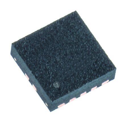
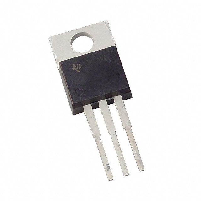
| 产品图片 |
|
| rohs | 符合RoHS无铅 / 符合限制有害物质指令(RoHS)规范要求 |
| 产品系列 | 电源管理 IC,低压差稳压器,Texas Instruments TPS74701DRCT- |
| 数据手册 | |
| 产品型号 | TPS74701DRCT |
| 产品目录页面 | |
| 产品种类 | 低压差稳压器 |
| 供应商器件封装 | 10-SON(3x3) |
| 其它名称 | 296-27071-2 |
| 制造商产品页 | http://www.ti.com/general/docs/suppproductinfo.tsp?distId=10&orderablePartNumber=TPS74701DRCT |
| 包装 | 带卷 (TR) |
| 单位重量 | 26.100 mg |
| 参考电压 | 0.804 V |
| 商标 | Texas Instruments |
| 回动电压—最大值 | 120 mV at 500 mA |
| 安装类型 | 表面贴装 |
| 安装风格 | SMD/SMT |
| 封装 | Reel |
| 封装/外壳 | 10-VFDFN 裸露焊盘 |
| 封装/箱体 | VSON-10 |
| 工作温度 | -40°C ~ 125°C |
| 工厂包装数量 | 250 |
| 最大功率耗散 | 1.92 W |
| 最大工作温度 | + 125 C |
| 最大输入电压 | 5.5 V |
| 最小工作温度 | - 40 C |
| 最小输入电压 | + 0.8 V |
| 标准包装 | 250 |
| 电压-跌落(典型值) | 0.05V @ 500mA |
| 电压-输入 | 0.8 V ~ 5.5 V |
| 电压-输出 | 0.8 V ~ 3.6 V |
| 电压调节准确度 | 0.5 % |
| 电流-输出 | 500mA |
| 电流-限制(最小值) | 800mA |
| 稳压器拓扑 | 正,可调式 |
| 稳压器数 | 1 |
| 系列 | TPS74701 |
| 线路调整率 | 0.03 % / V |
| 负载调节 | 0.09 % / A |
| 输出电压 | 800 mV to 3.6 V |
| 输出电流 | 500 mA |
| 输出端数量 | 1 Output |
| 输出类型 | Adjustable |
| 配用 | /product-detail/zh/TPS74701EVM-177/296-31288-ND/1908305 |


- 商务部:美国ITC正式对集成电路等产品启动337调查
- 曝三星4nm工艺存在良率问题 高通将骁龙8 Gen1或转产台积电
- 太阳诱电将投资9.5亿元在常州建新厂生产MLCC 预计2023年完工
- 英特尔发布欧洲新工厂建设计划 深化IDM 2.0 战略
- 台积电先进制程称霸业界 有大客户加持明年业绩稳了
- 达到5530亿美元!SIA预计今年全球半导体销售额将创下新高
- 英特尔拟将自动驾驶子公司Mobileye上市 估值或超500亿美元
- 三星加码芯片和SET,合并消费电子和移动部门,撤换高东真等 CEO
- 三星电子宣布重大人事变动 还合并消费电子和移动部门
- 海关总署:前11个月进口集成电路产品价值2.52万亿元 增长14.8%


PDF Datasheet 数据手册内容提取
Product Sample & Technical Tools & Support & Reference Folder Buy Documents Software Community Design TPS74701 SBVS099G–NOVEMBER2007–REVISEDOCTOBER2015 TPS74701 500-mA Low-Dropout Linear Regulator With Programmable Soft-Start 1 Features 3 Description • V Range:0.8Vto3.6V The TPS74701 low-dropout (LDO) linear regulator 1 OUT provides an easy-to-use, robust power management • UltralowV Range:0.8Vto5.5V IN solution for a wide variety of applications. User- • VBIASRange2.7Vto5.5V programmable soft-start minimizes stress on the input • LowDropout:50mVTypicallyat500mA,V = power source by reducing capacitive inrush current BIAS 5V on start-up. The soft-start is monotonic and well- suited for powering many different types of • PowerGood(PG)OutputAllowsSupply processors and ASICs. The enable input and power MonitoringorProvidesaSequencingSignalfor good output allow easy sequencing with external OtherSupplies regulators.Thiscompleteflexibilitypermitstheuserto • 2%AccuracyOverLine,Load,andTemperature configure a solution that meets the sequencing requirements of FPGAs, DSPs, and other • ProgrammableSoft-StartProvidesLinearVoltage applicationswithspecialstart-uprequirements. Start-Up • V PermitsLowV OperationWithGood A precision reference and error amplifier deliver 2% BIAS IN TransientResponse accuracy over load, line, temperature, and process. The device is stable with any type of capacitor • StableWithAnyOutputCapacitor≥ 2.2 μF greater than or equal to 2.2 μF, and is fully specified • AvailableinaSmall3-mm× 3-mm×1-mm10-Pin from –40°C to 125°C. The TPS74701 is offered in a Package small 3-mm × 3-mm SON-10 package for compatibilitywiththeTPS74801. 2 Applications DeviceInformation(1) • FPGAApplications PARTNUMBER PACKAGE BODYSIZE(NOM) • DSPCoreandI/OVoltages TPS74701 VSON(10) 3.00mm×3.00mm • Post-RegulationApplications (1) For all available packages, see the orderable addendum at • ApplicationsWithSpecialStart-UpTimeor theendofthedatasheet. SequencingRequirements • Hot-SwapandInrushControls TypicalApplicationCircuit(Adjustable) TurnonResponse C = 0nF SS C = 560pF SS VIN IN PG 0.5V/div CSS= 5600pF VOUT CIN BIAS R3 EN TPS74701 OUT VOUT VBIAS SS R1 C C GND FB OUT 3.8V BIAS V EN CSS R2 1V/div 1.8V Time (2ms/div) 1 An IMPORTANT NOTICE at the end of this data sheet addresses availability, warranty, changes, use in safety-critical applications, intellectualpropertymattersandotherimportantdisclaimers.PRODUCTIONDATA.
TPS74701 SBVS099G–NOVEMBER2007–REVISEDOCTOBER2015 www.ti.com Table of Contents 1 Features.................................................................. 1 8 ApplicationandImplementation........................ 14 2 Applications........................................................... 1 8.1 ApplicationInformation............................................14 3 Description............................................................. 1 8.2 TypicalApplication..................................................17 4 RevisionHistory..................................................... 2 9 PowerSupplyRecommendations...................... 18 5 PinConfigurationandFunctions......................... 3 10 Layout................................................................... 18 6 Specifications......................................................... 4 10.1 LayoutGuidelines.................................................18 6.1 AbsoluteMaximumRatings......................................4 10.2 LayoutExample....................................................18 6.2 ESDRatings..............................................................4 10.3 PowerDissipation.................................................18 6.3 RecommendedOperatingConditions.......................4 10.4 EstimatingJunctionTemperature ........................19 6.4 ThermalInformation..................................................5 11 DeviceandDocumentationSupport................. 21 6.5 ElectricalCharacteristics...........................................6 11.1 DeviceSupport......................................................21 6.6 TypicalCharacteristics:V =V ............................7 11.2 DocumentationSupport........................................21 EN IN 6.7 TypicalCharacteristics:V =V =1.8V,V = 11.3 CommunityResources..........................................21 EN IN OUT 1.5V.........................................................................10 11.4 Trademarks...........................................................21 7 DetailedDescription............................................ 11 11.5 ElectrostaticDischargeCaution............................21 7.1 Overview.................................................................11 11.6 Glossary................................................................22 7.2 FunctionalBlockDiagram.......................................11 12 Mechanical,Packaging,andOrderable 7.3 FeatureDescription.................................................11 Information........................................................... 22 7.4 DeviceFunctionalModes........................................13 4 Revision History NOTE:Pagenumbersforpreviousrevisionsmaydifferfrompagenumbersinthecurrentversion. ChangesfromRevisionF(November2010)toRevisionG Page • AddedESDRatingstable,FeatureDescriptionsection,DeviceFunctionalModes,ApplicationandImplementation section,PowerSupplyRecommendationssection,Layoutsection,DeviceandDocumentationSupportsection,and Mechanical,Packaging,andOrderableInformationsection ................................................................................................. 1 ChangesfromRevisionE(August,2010)toRevisionF Page • CorrectedequationforTable3............................................................................................................................................. 14 ChangesfromRevisionD(April,2009)toRevisionE Page • RevisedPowerDissipationsection...................................................................................................................................... 18 • Deleted(previouslynumbers)Figure28throughFigure30................................................................................................. 18 • Addedsection....................................................................................................................................................................... 19 2 SubmitDocumentationFeedback Copyright©2007–2015,TexasInstrumentsIncorporated ProductFolderLinks:TPS74701
TPS74701 www.ti.com SBVS099G–NOVEMBER2007–REVISEDOCTOBER2015 5 Pin Configuration and Functions DRCPackage 10-PinSON TopView IN 1 10 OUT IN 2 9 OUT Thermal PG 3 8 FB Pad BIAS 4 7 SS EN 5 6 GND PinFunctions PIN I/O DESCRIPTION NAME NO. IN 1,2 I Inputtothedevice. Enablepin.Drivingthispinhighenablestheregulator.Drivingthispinlowputstheregulator EN 5 I intoshutdownmode.Thispinmustnotbeleftunconnected. SS 7 — Soft-Startpin.Acapacitorconnectedonthispintogroundsetsthestart-uptime.Ifthispinis leftunconnected,theregulatoroutputsoft-startramptimeistypically200μs. BIAS 4 I Biasinputvoltageforerroramplifier,reference,andinternalcontrolcircuits. PowerGoodpin.Anopen-drain,active-highoutputthatindicatesthestatusofV .When OUT V exceedsthePGtripthreshold,thePGpingoesintoahigh-impedancestate.When OUT V isbelowthisthresholdthepinisdriventoalow-impedancestate.Apullupresistorfrom PG 3 O OUT 10kΩto1MΩshouldbeconnectedfromthispintoasupplyofupto5.5V.Thesupplycan behigherthantheinputvoltage.Alternatively,thePGpincanbeleftunconnectedifoutput monitoringisnotnecessary. Feedbackpin.Thefeedbackconnectiontothecentertapofanexternalresistordivider FB 8 I networkthatsetstheoutputvoltage.Thispinmustnotbeleftfloating. OUT 9,10 O Regulatedoutputvoltage.Asmallcapacitor(totaltypicalcapacitance≥2.2μF,ceramic)is neededfromthispintogroundtoassurestability. NC N/A I Noconnection.ThispincanbeleftfloatingorconnectedtoGNDtoallowbetterthermal contacttothetop-sideplane. GND 6 I Ground ThermalPad — I Shouldbesolderedtothegroundplaneforincreasedthermalperformance. Copyright©2007–2015,TexasInstrumentsIncorporated SubmitDocumentationFeedback 3 ProductFolderLinks:TPS74701
TPS74701 SBVS099G–NOVEMBER2007–REVISEDOCTOBER2015 www.ti.com 6 Specifications 6.1 Absolute Maximum Ratings AtT =–40°Cto125°C,unlessotherwisenoted.AllvoltagesarewithrespecttoGND.(1) J MIN MAX UNIT V ,V Inputvoltage –0.3 6 V IN BIAS V Enablevoltage –0.3 6 V EN V Powergoodvoltage –0.3 6 V PG I PGsinkcurrent 0 1.5 mA PG V Soft-startvoltage –0.3 6 V SS V Feedbackvoltage –0.3 6 V FB V Outputvoltage –0.3 V +0.3 V OUT IN I Maximumoutputcurrent Internallylimited OUT Outputshort-circuitduration Indefinite P Continuoustotalpowerdissipation SeeThermalInformation DISS T Operatingjunctiontemperature –40 125 °C J T Storagetemperature –55 150 °C stg (1) StressesbeyondthoselistedunderAbsoluteMaximumRatingsmaycausepermanentdamagetothedevice.Thesearestressratings only,whichdonotimplyfunctionaloperationofthedeviceattheseoranyotherconditionsbeyondthoseindicatedunderRecommended OperatingConditions.Exposuretoabsolute-maximum-ratedconditionsforextendedperiodsmayaffectdevicereliability. 6.2 ESD Ratings VALUE UNIT Humanbodymodel(HBM),perANSI/ESDA/JEDECJS-001,allpins(1) ±2000 V(ESD) Electrostaticdischarge Chargeddevicemodel(CDM),perJEDECspecificationJESD22-C101,all V pins(2) ±500 (1) JEDECdocumentJEP155statesthat500-VHBMallowssafemanufacturingwithastandardESDcontrolprocess. (2) JEDECdocumentJEP157statesthat250-VCDMallowssafemanufacturingwithastandardESDcontrolprocess. 6.3 Recommended Operating Conditions overoperatingjunctiontemperaturerange(unlessotherwisenoted) MIN NOM MAX UNIT V Inputsupplyvoltage V +V (V ) V +0.3 5.5 V IN OUT DO IN OUT V Enablesupplyvoltage 0 V 5.5 V EN IN V (1) BIASsupplyvoltage V +V (V )(2) V +1.4(2) 5.5 V BIAS OUT DO BIAS OUT V Outputvoltage 0.8 3.3 V OUT I Outputcurrent 0 500 mA OUT C Outputcapacitor 2.2 µF OUT C Inputcapacitor(3) 1 µF IN C Biascapacitor 0.1 1 µF BIAS T Operatingjunctiontemperature –40 125 °C J (1) BIASsupplyisrequiredwhenV isbelowV +1.62V. IN OUT (2) V hasaminimumvoltageof2.7VorV +V (V ),whicheverishigher. BIAS OUT DO BIAS (3) IfV andV areconnectedtothesamesupply,therecommendedminimumcapacitorforthesupplyis4.7μF. IN BIAS 4 SubmitDocumentationFeedback Copyright©2007–2015,TexasInstrumentsIncorporated ProductFolderLinks:TPS74701
TPS74701 www.ti.com SBVS099G–NOVEMBER2007–REVISEDOCTOBER2015 6.4 Thermal Information TPS74701 THERMALMETRIC(1)(2) DRC(VSON)(3) UNIT 10PINS R Junction-to-ambientthermalresistance 41.5 °C/W θJA R Junction-to-case(top)thermalresistance 78 °C/W θJC(top) R Junction-to-boardthermalresistance N/A °C/W θJB ψ Junction-to-topcharacterizationparameter 0.7 °C/W JT ψ Junction-to-boardcharacterizationparameter 11.3 °C/W JB R Junction-to-case(bottom)thermalresistance 6.6 °C/W θJC(bot) (1) Formoreinformationabouttraditionalandnewthermalmetrics,seetheSemiconductorandICPackageThermalMetricsapplication report,SPRA953. (2) ForthermalestimatesofthisdevicebasedonPCBcopperarea,seetheTIPCBThermalCalculator. (3) ThermaldatafortheDRCpackagearederivedbythermalsimulationsbasedonJEDEC-standardmethodologyasspecifiedinthe JESD51series.Thefollowingassumptionsareusedinthesimulations: (a)TheexposedpadisconnectedtothePCBgroundlayerthrougha3×2thermalviaarray. (b)Thetopandbottomcopperlayersareassumedtohavea20%thermalconductivityofcopperrepresentinga20%coppercoverage. (c)ThisdataweregeneratedwithonlyasingledeviceatthecenterofaJEDEChigh-K(2s2p)boardwith3-inches×3-inchescopper area. To understand the effects of the copper area on thermal performance, see the Power Dissipation and Estimating Junction Temperaturesections. Copyright©2007–2015,TexasInstrumentsIncorporated SubmitDocumentationFeedback 5 ProductFolderLinks:TPS74701
TPS74701 SBVS099G–NOVEMBER2007–REVISEDOCTOBER2015 www.ti.com 6.5 Electrical Characteristics AtV =1.1V,V =V +0.3V,C =0.1μF,C =C =10μF,C =1nF,I =50mA,V =5V,andT =–40°C EN IN OUT BIAS IN OUT NR OUT BIAS J to125°C,unlessotherwisenoted.TypicalvaluesareatT =25°C. J PARAMETER TESTCONDITIONS MIN TYP MAX UNIT V Inputvoltagerange V +V 5.5 V IN OUT DO V Biaspinvoltagerange 2.7 5.5 V BIAS Internalreference V T =25°C 0.796 0.8 0.804 V REF (Adjustable) J Outputvoltagerange V =5V,I =500mA V 3.6 V IN OUT REF VOUT Accuracy(1) 2.97V≤VBIAS≤5.5V, –2% ±0.5% 2% 50mA≤I ≤500mA OUT V /V Lineregulation V +0.3≤V ≤5.5V 0.03 %/V OUT IN OUT(NOM) IN V /I Loadregulation 50mA≤I ≤500mA 0.09 %/A OUT OUT OUT VDO VINdropoutvoltage(2) IVOBUIATS=–5V0O0UmTA(N,OM)≥1.62V(3) 50 120 mV V dropoutvoltage(2) I =500mA,V =V 1.31 1.39 V BIAS OUT IN BIAS I Currentlimit V =80%×V 800 1350 mA CL OUT OUT(NOM) I Biaspincurrent 1 2 mA BIAS Shutdownsupplycurrent I V ≤0.4V 1 50 μA SHDN (I ) EN GND I Feedbackpincurrent –1 0.150 1 μA FB 1kHz,I =500mA, OUT 60 Power-supplyrejection VIN=1.8V,VOUT=1.5V dB (VINtoVOUT) 300kHz,IOUT=500mA, 30 V =1.8V,V =1.5V IN OUT PSRR 1kHz,I =500mA, OUT 50 Power-supplyrejection VIN=1.8V,VOUT=1.5V dB (VBIAStoVOUT) 300kHz,IOUT=500mA, 30 V =1.8V,V =1.5V IN OUT 100Hzto100kHz, Noise Outputnoisevoltage 25×V μV I =500mA,C =0.001μF OUT RMS OUT SS t Minimumstart-uptime R forI =1A,C =open 200 μs STR LOAD OUT SS I Soft-startchargingcurrent V =0.4V 440 nA SS SS V Enableinputhighlevel 1.1 5.5 V EN,HI V Enableinputlowlevel 0 0.4 V EN,LO V Enablepinhysteresis 50 mV EN,HYS V Enablepindeglitchtime 20 μs EN,DG I Enablepincurrent V =5V 0.1 1 μA EN EN V PGtripthreshold V decreasing 85 90 94 %V IT OUT OUT V PGtriphysteresis 3 %V HYS OUT V PGoutputlowvoltage I =1mA(sinking),V <V 0.3 V PG,LO PG OUT IT I PGleakagecurrent V =5.25V,V >V 0.1 1 μA PG,LKG PG OUT IT Operatingjunction T –40 125 °C J temperature Thermalshutdown Shutdown,temperatureincreasing 165 T °C SD temperature Reset,temperaturedecreasing 140 (1) Adjustabledevicestestedat0.8V;resistortoleranceisnottakenintoaccount. (2) DropoutisdefinedasthevoltagefromV toV whenV is3%lessthannominal. IN OUT OUT (3) 1.62VisatestconditionofthisdeviceandcanbeadjustedbyreferringtoFigure6. 6 SubmitDocumentationFeedback Copyright©2007–2015,TexasInstrumentsIncorporated ProductFolderLinks:TPS74701
TPS74701 www.ti.com SBVS099G–NOVEMBER2007–REVISEDOCTOBER2015 6.6 Typical Characteristics: V = V EN IN AtT =25°C,V =V +0.3V,V =5V,I =50mA,V =V ,C =1μF,C =4.7μF,andC =10μF, J IN OUT(TYP) BIAS OUT EN IN IN BIAS OUT unlessotherwisenoted. 0.20 0.5 0.4 0.15 0.3 0.10 %) -40°C %) 0.2 ( ( -40°C UT 0.05 UT 0.1 O O V V n 0 n 0 ange i -0.05 +25°C +125°C ange i -0.1 +125°C +25°C Ch -0.01 Ch -0.2 -0.3 -0.15 -0.4 -0.20 -0.5 0 0.5 1.0 1.5 2.0 2.5 3.0 3.5 4.0 4.5 5.0 0.5 1.0 1.5 2.0 2.5 3.0 3.5 4.0 V -V (V) V -V (V) IN OUT BIAS OUT Figure1.V LineRegulation Figure2.V LineRegulation IN BIAS 1.2 0.5 0.4 1.0 0.3 %) %) 0.2 ( 0.8 ( +125°C UT UT 0.1 O O V V n 0.6 n 0 Change i 0.4 Change i --00..12 -40°C +25°C -0.3 0.2 -0.4 0 -0.5 0 10 20 30 40 50 0 100 200 300 400 500 I (mA) I (mA) OUT OUT Figure3.LoadRegulation Figure4.LoadRegulation 100 200 I = 0.5A OUT 90 180 80 160 V) V) m 70 m 140 ) (UT 60 ()UT 120 O O V 50 V 100 - - +25°C (VIN 40 +125°C (VIN 80 +125°C VDO 30 +25°C VDO 60 20 40 -40°C 10 20 -40°C 0 0 0 100 200 300 400 500 0 0.5 1.0 1.5 2.0 2.5 3.0 3.5 4.0 4.5 I (mA) V -V (V) OUT BIAS OUT Figure5.DropoutVoltagevsI andTemperature(T ) Figure6.DropoutVoltagevs(V –V )and OUT J BIAS OUT Temperature(T ) J Copyright©2007–2015,TexasInstrumentsIncorporated SubmitDocumentationFeedback 7 ProductFolderLinks:TPS74701
TPS74701 SBVS099G–NOVEMBER2007–REVISEDOCTOBER2015 www.ti.com Typical Characteristics: V = V (continued) EN IN AtT =25°C,V =V +0.3V,V =5V,I =50mA,V =V ,C =1μF,C =4.7μF,andC =10μF, J IN OUT(TYP) BIAS OUT EN IN IN BIAS OUT unlessotherwisenoted. 2200 90 2000 B) 80 d I = 0.1A mV) 1800 atio ( 70 OUT -V) (SOUT 11640000 +125°C Rejection R 654000 V(VDOBIA 11200000 +25°C -40°C wer-Supply 3200 VVIONU=T =1 .18.V2V IOUT= 0.5A 800 Po 10 VBIAS= 5V C = 1nF SS 600 0 0 100 200 300 400 500 10 100 1k 10k 100k 1M 10M I (mA) Frequency (Hz) OUT Figure7.V DropoutVoltagevsI andTemperature Figure8.V PSRRvsFrequency BIAS OUT BIAS (T ) J 90 90 B) 80 B) 80 d d atio ( 70 atio ( 70 1kHz R R ction 6500 IOUT= 100mA ction 6500 10kHz e e ej ej R 40 R 40 pply 30 pply 30 100kHz u V = 1.8V u S IN S 500kHz Power- 2100 VCCOOSSUUTT=== 1 11n.0F2mVF IOUT= 500mA Power- 2100 IOVUTOCU=ST S5=0= 01 1m.2nAVF 0 0 10 100 1k 10k 100k 1M 10M 0 0.25 0.50 0.75 1.00 1.25 1.50 1.75 2.00 2.25 Frequency (Hz) V -V (V) IN OUT Figure9.V PSRRvsFrequency Figure10.V PSRRvs(V –V ) IN IN IN OUT 1 2.0 ÖV/)Hz IVOOUUTT== 1 10.02mVA 1.8 +125°C m 1.6 y ( sit 1.4 n e De CSS= 0nF mA) 1.2 ois 0.1 (S 1.0 ctral N IBIA 00..86 +25°C Spe CSS= 10nF C = 1nF 0.4 -40°C ut SS utp 0.2 O 0.01 0 100 1k 10k 100k 0 100 200 300 400 500 Frequency (Hz) I (mA) OUT Figure11.NoiseSpectralDensity Figure12.BIASPinCurrentvsI andTemperature(T ) OUT J 8 SubmitDocumentationFeedback Copyright©2007–2015,TexasInstrumentsIncorporated ProductFolderLinks:TPS74701
TPS74701 www.ti.com SBVS099G–NOVEMBER2007–REVISEDOCTOBER2015 Typical Characteristics: V = V (continued) EN IN AtT =25°C,V =V +0.3V,V =5V,I =50mA,V =V ,C =1μF,C =4.7μF,andC =10μF, J IN OUT(TYP) BIAS OUT EN IN IN BIAS OUT unlessotherwisenoted. 2.0 500 1.8 +125°C 475 1.6 450 1.4 mA) 1.2 +25°C A) 425 I(BIAS 10..08 I(nSS 430705 0.6 -40°C 350 0.4 325 0.2 0 300 2.0 2.5 3.0 3.5 4.0 4.5 5.0 5.5 -50 -25 0 25 50 75 100 125 V (V) Junction Temperature (°C) BIAS Figure13.BIASPinCurrentvsV andTemperature(T ) Figure14.Soft-StartChargingCurrent(I )vsTemperature BIAS J SS (T ) J 1.0 1.5 V = 0.8V OUT 0.9 1.4 V) ge ( 0.8 1.3 +125°C G Volta 00..76 mit (A) 11..21 ow-Level P 000...543 Current Li 100...098 -40°C +25°C L OL 0.2 0.7 V 0.1 0.6 0 0.5 0 2 4 6 8 10 12 1.0 1.5 2.0 2.5 3.0 3.5 4.0 4.5 5.0 PG Current (mA) VBIAS-VOUT(V) Figure15.Low-LevelPGVoltagevsCurrent Figure16.CurrentLimitvs(VBIAS–VOUT) Copyright©2007–2015,TexasInstrumentsIncorporated SubmitDocumentationFeedback 9 ProductFolderLinks:TPS74701
TPS74701 SBVS099G–NOVEMBER2007–REVISEDOCTOBER2015 www.ti.com 6.7 Typical Characteristics: V = V = 1.8 V, V = 1.5 V EN IN OUT AtT =25°C,V =V +0.3V,V =5V,I =50mA,V =V =1.8V,V =1.5V,C =1μF,C =4.7μF, J IN OUT(TYP) BIAS OUT EN IN OUT IN BIAS andC =10μF,unlessotherwisenoted. OUT C = 1nF SS COUT= 2.2mF (Ceramic) COUT= 2.2mF (Ceramic) 50mV/div 50mV/div C = 1nF SS 3.8V 5.0V 1V/div 1V/div 3.3V 1V/ms 1.8V 1V/ms Time (50ms/div) Time (50ms/div) Figure17.V LineTransient Figure18.V LineTransient BIAS IN C = 470mF (OSCON) C = 0nF OUT SS 100mV/div C = 560pF SS C = 1nF SS 0.5V/div CSS= 5600pF VOUT 100mV/div C = 10mF (Ceramic) OUT 100mV/div C = 2.2mF (Ceramic) 3.8V OUT V EN 1V/div 1.8V 500mA/div 50mA 1A/ms Time (50ms/div) Time (2ms/div) Figure19.OutputLoadTransientResponse Figure20.TurnonResponse V = V = V IN BIAS EN v di V/ 1 V OUT V PG Time (20ms/div) Figure21.PowerUpandPowerDown 10 SubmitDocumentationFeedback Copyright©2007–2015,TexasInstrumentsIncorporated ProductFolderLinks:TPS74701
TPS74701 www.ti.com SBVS099G–NOVEMBER2007–REVISEDOCTOBER2015 7 Detailed Description 7.1 Overview The TPS74701 belongs to a family of low-dropout regulators that feature soft-start capability. These regulators use a low current bias input to power all internal control circuitry, allowing the NMOS pass transistor to regulate verylowinputandoutputvoltages. TheuseofanNMOS-passFEToffersseveralcriticaladvantagesformanyapplications.UnlikeaPMOStopology device, the output capacitor has little effect on loop stability. This architecture allows the TPS74701 to be stable with any capacitor type of value 2.2 μF or greater. Transient response is also superior to PMOS topologies, particularlyforlowV applications. IN The TPS74701 features a programmable voltage-controlled soft-start circuit that provides a smooth, monotonic start-up and limits start-up inrush currents that may be caused by large capacitive loads. A power good (PG) output is available to allow supply monitoring and sequencing of other supplies. An enable (EN) pin with hysteresis and deglitch allows slow-ramping signals to be used for sequencing the device. The low VIN and VOUT capability allows for inexpensive, easy-to-design, and efficient linear regulation between the multiple supplyvoltagesoftenpresentinprocessor-intensivesystems. 7.2 Functional Block Diagram Current OUT IN Limit VOUT BIAS UVLO Thermal 0.44mA Limit R1 SS C SS Soft-Start 0.8V Discharge Reference FB PG Hysteresis EN and Deglitch R2 0.9´V REF GND 7.3 Feature Description 7.3.1 ProgrammableSoft-Start The TPS74701 features a programmable, monotonic, voltage-controlled soft-start that is set with an external capacitor (C ). This feature is important for many applications because it eliminates power-up initialization SS problems when powering FPGAs, DSPs, or other processors. The controlled voltage ramp of the output also reducespeakinrushcurrentduringstart-up,minimizingstart-uptransienteventstotheinputpowerbus. To achieve a linear and monotonic soft-start, the TPS74701 error amplifier tracks the voltage ramp of the external soft-start capacitor until the voltage exceeds the internal reference. The soft-start ramp time depends on the soft-start charging current (I ), soft-start capacitance (C ), and the internal reference voltage (V ), and SS SS REF canbecalculatedusingEquation1: Copyright©2007–2015,TexasInstrumentsIncorporated SubmitDocumentationFeedback 11 ProductFolderLinks:TPS74701
TPS74701 SBVS099G–NOVEMBER2007–REVISEDOCTOBER2015 www.ti.com Feature Description (continued) (V ´C ) t = REF SS SS I SS (1) If large output capacitors are used, the device current limit (I ) and the output capacitor may set the start-up CL time.Inthiscase,thestart-uptimeisgivenbyEquation2: (V ´C ) OUT(NOM) OUT t = SSCL I CL(MIN) where • V isthenominaloutputvoltage OUT(NOM) • C istheoutputcapacitance OUT • I istheminimumcurrentlimitforthedevice (2) CL(MIN) Inapplicationswheremonotonicstart-upisrequired,thesoft-starttimegivenbyEquation1 shouldbesetgreater thanEquation2. The maximum recommended soft-start capacitor is 0.015 μF. Larger soft-start capacitors can be used, and they do not damage the device; however, the soft-start capacitor discharge circuit may not be able to fully discharge thesoft-startcapacitorwhenenabled. Soft-start capacitors larger than 0.015 μF could be a problem in applications where it is necessary to rapidly pulsetheenablepinandstillrequirethedevicetosoft-startfromground.C mustbelow-leakage;X7R,X5R,or SS C0Gdielectricmaterialsarepreferred.SeeTable3forsuggestedsoft-startcapacitorvalues. 7.3.2 EnableandShutdown The enable (EN) pin is active high and is compatible with standard digital signaling levels. V below 0.4 V turns EN the regulator off, while V above 1.1 V turns the regulator on. Unlike many regulators, the enable circuitry has EN hysteresis and deglitching for use with relatively slowly ramping analog signals. This configuration allows the TPS74701 to be enabled by connecting the output of another supply to the EN pin. The enable circuitry typically has 50 mV of hysteresis and a deglitch circuit to help avoid on-off cycling as a result of small glitches in the V EN signal. The enable threshold is typically 0.8 V and varies with temperature and process variations. Temperature variation is approximately –1 mV/°C; process variation accounts for most of the rest of the variation to the 0.4-V and 1.1-V limits. If precise turnon timing is required, a fast rise-time signal must be used to enable the TPS74701. If not used, EN can be connected to either IN or BIAS. If EN is connected to IN, it should be connected as close as possible to the largest capacitance on the input to prevent voltage droops on that line from triggering the enablecircuit. 7.3.3 PowerGood The power good (PG) pin is an open-drain output and can be connected to any 5.5 V or lower rail through an external pullup resistor. This pin requires at least 1.1 V on V to have a valid output. The PG output is high- BIAS impedancewhenV isgreaterthanV +V .IfV dropsbelowV orifV dropsbelow1.9V,theopen- OUT IT HYS OUT IT BIAS drain output turns on and pulls the PG output low. The PG pin also asserts when the device is disabled. The recommended operating condition of the PG pin sink current is up to 1 mA, so the pullup resistor for PG should beintherangeof10kΩ to1MΩ.Ifoutputvoltagemonitoringisnotneeded,thePGpincanbeleftfloating. 7.3.4 InternalCurrentLimit The TPS74701 features a factory-trimmed, accurate current limit that is flat over temperature and supply voltage. The current limit allows the device to supply surges of up to 1 A and maintain regulation. The current limit respondsinabout10μstoreducethecurrentduringashort-circuitfault. The internal current limit protection circuitry of the TPS74701 is designed to protect against overload conditions. It is not intended to allow operation above the rated current of the device. Continuously running the TPS74701 abovetheratedcurrentdegradesdevicereliability. 12 SubmitDocumentationFeedback Copyright©2007–2015,TexasInstrumentsIncorporated ProductFolderLinks:TPS74701
TPS74701 www.ti.com SBVS099G–NOVEMBER2007–REVISEDOCTOBER2015 Feature Description (continued) 7.3.5 ThermalShutdown Thermal protection disables the output when the junction temperature rises to approximately 160°C, allowing the device to cool. When the junction temperature cools to approximately 140°C, the output circuitry is enabled. Depending on power dissipation, thermal resistance, and ambient temperature the thermal protection circuit may cycle on and off. This cycling limits the dissipation of the regulator, protecting it from damage as a result of overheating. Activation of the thermal protection circuit indicates excessive power dissipation or inadequate heatsinking. For reliable operation, junction temperature should be limited to 125°C maximum. To estimate the margin of safety in a complete design (including heatsink), increase the ambient temperature until thermal protection is triggered; use worst-case loads and signal conditions. For good reliability, thermal protection should trigger at least 40°C abovethemaximumexpectedambientconditionoftheapplication.Thisconditionproducesaworst-casejunction temperatureof125°Catthehighestexpectedambienttemperatureandworst-caseload. The internal protection circuitry of the TPS74701 is designed to protect against overload conditions. It is not intended to replace proper heatsinking. Continuously running the TPS74701 into thermal shutdown degrades devicereliability. 7.4 Device Functional Modes 7.4.1 NormalOperation Thedeviceregulatestothenominaloutputvoltageunderthefollowingconditions: • Theinputvoltageandbiasvoltagearebothatleastattherespectiveminimumspecifications. • The enable voltage has previously exceeded the enable rising threshold voltage and has not decreased belowtheenablefallingthreshold. • Theoutputcurrentislessthanthecurrentlimit. • Thedevicejunctiontemperatureislessthanthemaximumspecifiedjunctiontemperature. 7.4.2 DropoutOperation If the input voltage is lower than the nominal output voltage plus the specified dropout voltage, but all other conditions are met for normal operation, the device operates in dropout mode. In this condition, the output voltage is the same as the input voltage minus the dropout voltage. The transient performance of the device is significantly degraded because the pass device is in a triode state and no longer controls the current through the LDO.Lineorloadtransientsindropoutcanresultinlargeoutputvoltagedeviations. 7.4.3 Disabled Thedeviceisdisabledunderthefollowingconditions: • Theinputorbiasvoltagesarebelowtherespectiveminimumspecifications. • The enable voltage is less than the enable falling threshold voltage or has not yet exceeded the enable rising threshold. • Thedevicejunctiontemperatureisgreaterthanthethermalshutdowntemperature. Table1showstheconditionsthatleadtothedifferentmodesofoperation. Table1.DeviceFunctionalModeComparison PARAMETER OPERATINGMODE V V V I T IN EN BIAS OUT J Normalmode V >V +V (V ) V >V V ≥V +1.39V I <I T <125°C IN OUT(nom) DO IN EN EN,HI BIAS OUT OUT CL J Dropoutmode V <V +V (V ) V >V V <V +1.39V — T <125°C IN OUT(nom) DO IN EN EN,HI BIAS OUT J Disabledmode (anytrueconditiondisables V <V V <V V <V — T >165°C IN IN(min) EN EN,LO BIAS BIAS(min) J thedevice) Copyright©2007–2015,TexasInstrumentsIncorporated SubmitDocumentationFeedback 13 ProductFolderLinks:TPS74701
TPS74701 SBVS099G–NOVEMBER2007–REVISEDOCTOBER2015 www.ti.com 8 Application and Implementation NOTE Information in the following applications sections is not part of the TI component specification, and TI does not warrant its accuracy or completeness. TI’s customers are responsible for determining suitability of components for their purposes. Customers should validateandtesttheirdesignimplementationtoconfirmsystemfunctionality. 8.1 Application Information R and R can be calculated for any output voltage using the formula shown in Figure 25. See Table 2 for 1 2 sample resistor values of common output voltages. To achieve the maximum accuracy specifications, R should 2 belessthanorequalto4.99kΩ. Table2.Standard1%ResistorValuesforProgramming theOutputVoltage(1) R (kΩ) R (kΩ) V (V) 1 2 OUT Short Open 0.8 0.619 4.99 0.9 1.13 4.53 1 1.37 4.42 1.05 1.87 4.99 1.1 2.49 4.99 1.2 4.12 4.75 1.5 3.57 2.87 1.8 3.57 1.69 2.5 3.57 1.15 3.3 (1) V =0.8×(1+R /R ). OUT 1 2 Table3.StandardCapacitorValuesforProgramming theSoft-StartTime(1) C SOFT-STARTTIME SS Open 0.1ms 270pF 0.5ms 560pF 1ms 2.7nF 5ms 5.6nF 10ms 0.01μF 18ms V ×C 0.8V×C (F) t (s) = REF SS = SS SS I 0.44mA (1) SS wheretSS(s)=soft-start timeinseconds. 8.1.1 Input,Output,andBiasCapacitorRequirements The device is designed to be stable for all available types and values of output capacitors greater than or equal to2.2μF.Thedeviceisalsostablewithmultiplecapacitorsinparallel,whichcanbeofanytypeorvalue. The capacitance required on the IN and BIAS pins strongly depends on the input supply source impedance. To counteract any inductance in the input, the minimum recommended capacitor for V and V is 1 μF. If V and IN BIAS IN V are connected to the same supply, the recommended minimum capacitor for V is 4.7 μF. Good quality, BIAS BIAS low ESR capacitors should be used on the input; ceramic X5R and X7R capacitors are preferred. These capacitorsshouldbeplacedasclosethepinsaspossibleforoptimumperformance. 14 SubmitDocumentationFeedback Copyright©2007–2015,TexasInstrumentsIncorporated ProductFolderLinks:TPS74701
TPS74701 www.ti.com SBVS099G–NOVEMBER2007–REVISEDOCTOBER2015 8.1.2 TransientResponse The TPS74701 was designed to have excellent transient response for most applications with a small amount of output capacitance. In some cases, the transient response may be limited by the transient response of the input supply. This limitation is especially true in applications where the difference between the input and output is less than 300 mV. In this case, adding additional input capacitance improves the transient response much more than just adding additional output capacitance would do. With a solid input supply, adding additional output capacitance reduces undershoot and overshoot during a transient event; see Figure 19 in the Typical Characteristics: V = V section. Because the TPS74701 is stable with output capacitors as low as 2.2 μF, EN IN many applications may then need very little capacitance at the LDO output. For these applications, local bypass capacitance for the powered device may be sufficient to meet the transient requirements of the application. This design reduces the total solution cost by avoiding the need to use expensive, high-value capacitors at the LDO output. 8.1.3 DropoutVoltage The TPS74701 offers very low dropout performance, making it well-suited for high-current, low V /low V IN OUT applications. The low dropout of the TPS74701 allows the device to be used in place of a DC-DC converter and still achieve good efficiency. This feature provides designers with the power architecture for their applications to achievethesmallest,simplest,andlowestcostsolution. There are two different specifications for dropout voltage with the TPS74701. The first specification (shown in Figure 22) is referred to as V Dropout and is used when an external bias voltage is applied to achieve low IN dropout. This specification assumes that V is at least 1.39 V (2) above V , which is the case for V when BIAS OUT BIAS powered by a 3.3-V rail with 5% tolerance and with V = 1.5 V. If V is higher than V +1.39 V(1), V OUT BIAS OUT IN dropoutislessthanspecified. BIAS IN V = 5V ±5% BIAS V = 1.8V IN V = 1.5V OUT I = 500 mA Reference OUT Efficiency = 83% OUT V OUT C OUT FB Simplified Block Diagram Figure22. TypicalApplicationoftheTPS74701UsinganAuxiliaryBiasRail V IN V = 3.3V ±5% BIAS IN BIAS V = 3.3V ± 5V IN V = 1.5V OUT I = 500 mA Reference OUT Efficiency = 45% OUT V OUT C OUT FB Simplified Block Diagram Figure23. TypicalApplicationoftheTPS74701WithoutanAuxiliaryBiasRail (2) 1.62VisatestconditionofthisdeviceandcanbeadjustedbyreferringtoFigure6. Copyright©2007–2015,TexasInstrumentsIncorporated SubmitDocumentationFeedback 15 ProductFolderLinks:TPS74701
TPS74701 SBVS099G–NOVEMBER2007–REVISEDOCTOBER2015 www.ti.com The second specification (shown in Figure 23) is referred to as V Dropout and applies to applications where BIAS IN and BIAS are tied together. This option allows the device to be used in applications where an auxiliary bias voltage is not available or low dropout is not required. Dropout is limited by BIAS in these applications because V provides the gate drive to the pass FET; therefore, V must be 1.39-V above V . Because of this BIAS BIAS OUT usage, IN and BIAS tied together easily consume huge power. Pay attention not to exceed the power rating of theICpackage. 8.1.4 SequencingRequirements V , V , and V can be sequenced in any order without causing damage to the device. However, for the soft- IN BIAS EN start function to work as intended, certain sequencing rules must be applied. Connecting EN to IN is acceptable for most applications, as long as V is greater than 1.1 V and the ramp rate of V and V is faster than the IN IN BIAS set soft-start ramp rate. If the ramp rate of the input sources is slower than the set soft-start time, the output tracks the slower supply minus the dropout voltage until it reaches the set output voltage. If EN is connected to BIAS, the device soft-starts as programmed, provided that V is present before V . If V and V are IN BIAS BIAS EN present before V is applied and the set soft-start time has expired, then V tracks V . If the soft-start time IN OUT IN has not expired, the output tracks V until V reaches the value set by the charging soft-start capacitor. IN OUT Figure 24 shows the use of an RC-delay circuit to hold off V until V has ramped. This technique can also EN BIAS be used to drive EN from V . An external control signal can also be used to enable the device after V and IN IN V arepresent. BIAS NOTE WhenV andV arepresentandV isnotsupplied,thisdeviceoutputsapproximately BIAS EN IN 50 μA of current from OUT. Although this condition does not cause any damage to the device, the output current may charge up the OUT node if total resistance between OUT andGND(includingexternalfeedbackresistors)isgreaterthan10kΩ. VIN IN OUT VOUT CIN R1 C BIAS TPS74701 FB OUT VBIAS R R2 C EN GND SS BIAS C CSS Figure24. Soft-StartDelayUsinganRCCircuittoEnabletheDevice 8.1.5 OutputNoise The TPS74701 provides low-output noise when a soft-start capacitor is used. When the device reaches the end of the soft-start cycle, the soft-start capacitor serves as a filter for the internal reference. By using a 0.001-μF soft-start capacitor, the output noise is reduced by half and is typically 30 μV for a 1.2-V output (10 Hz to 100 RMS kHz). Further increasing C has little effect on noise. Because most of the output noise is generated by the SS internal reference, the noise is a function of the set output voltage. The RMS noise with a 0.001-μF soft-start capacitorisgiveninEquation3: V (mV ) = 25(mVRMS)x V (V) N RMS OUT V (3) The low-output noise of the TPS74701 makes it a good choice for powering transceivers, PLLs, or other noise- sensitivecircuitry. 16 SubmitDocumentationFeedback Copyright©2007–2015,TexasInstrumentsIncorporated ProductFolderLinks:TPS74701
TPS74701 www.ti.com SBVS099G–NOVEMBER2007–REVISEDOCTOBER2015 8.2 Typical Application Figure25illustratesthetypicalapplicationcircuitfortheTPS74701adjustableoutputdevice. VIN IN PG C1mINF BIAS R3 EN TPS74701 OUT VOUT VBIAS SS R1 COUT CBIAS GND FB 10mF 1mF CSS R2 V = 0.8´(1 + R1 ) OUT R 2 Figure25. TypicalApplicationCircuitfortheTPS74701(Adjustable) 8.2.1 DesignRequirements Table4showsthedesignparametersforthisapplication. Table4.DesignParameters DESIGNPARAMETER EXAMPLEVALUE VIN 1.8V±10% VBIAS 3.3V±10% VOUT 1.5V±3% IOUT 500mA Start-uptime <2ms 8.2.2 DetailedDesignProcedure 1. Select R1 and R2 based on the required output voltage. Table 2 gives example calculations for many commonoutputvoltages. 2. Select C to be the highest capacitance while still achieving the desired start-up time. Table 3 gives SS examplesofthiscalculation. 3. Select a minimum of a 2.2-µF ceramic output capacitor. Increased output capacitance will help the output load transient response. Figure 27 gives examples of the load transient response with different output capacitorvaluesandtypes. 8.2.3 ApplicationCurves C = 470mF (OSCON) C = 0nF OUT SS 100mV/div C = 560pF SS C = 1nF SS 0.5V/div CSS= 5600pF VOUT 100mV/div C = 10mF (Ceramic) OUT 100mV/div C = 2.2mF (Ceramic) 3.8V OUT V EN 1V/div 1.8V 500mA/div 50mA 1A/ms Time (50ms/div) Time (2ms/div) Figure26.OutputLoadTransientResponse Figure27.TurnonResponse Copyright©2007–2015,TexasInstrumentsIncorporated SubmitDocumentationFeedback 17 ProductFolderLinks:TPS74701
TPS74701 SBVS099G–NOVEMBER2007–REVISEDOCTOBER2015 www.ti.com 9 Power Supply Recommendations The TPS74701 is designed to operate from an input voltage up to 5.5 V, provided the bias rail is at least 1.39-V higher than the input supply and dropout requirements are met. The bias rail and the input supply should both provide adequate headroom and current for the device to operate normally. Connect a low-output impedance powersupplydirectlytotheINpinoftheTPS74701.Thissupplymusthaveatleast1 μFofcapacitancenearthe INpinforoptimalperformance.Asupplywithsimilarrequirementsmustalsobeconnecteddirectlytothebiasrail with a separate 1-μF or larger capacitor. If the IN pin is tied to the bias pin, a minimum 4.7 μF of capacitance is needed for performance. To increase the overall PSRR of the solution at higher frequencies, use a pi-filter or ferritebeadbeforetheinputcapacitor. 10 Layout 10.1 Layout Guidelines An optimal layout can greatly improve transient performance, PSRR, and noise. To minimize the voltage droop on the input of the device during load transients, connect the capacitance on IN, OUT and BIAS as close as possible to the device. If BIAS is connected to IN, connect BIAS as close to the input supply as possible. This connection minimizes the voltage droop on BIAS during transient conditions and can improve the turnon response. 10.2 Layout Example CIN Input GND Plane IN 1 10 OUT Vout Vin IN 2 9 OUT R1 COUT PG 3 8 FB CBIAS BIAS 4 7 SS Css R2 EN 5 6 GND Output GND Plane Note: CIN, COUT,and CBIAS are 0603 case size capacitors, while CSS, R1, and R2 are 0402 case size. Figure28. TPS547LayoutRecommendation 10.3 Power Dissipation An optimal layout can greatly improve transient performance, PSRR, and noise. To minimize the voltage drop on the input of the device during load transients, the capacitance on IN and BIAS should be connected as close as possible to the device. This capacitance also minimizes the effects of parasitic inductance and resistance of the input source and can therefore improve stability. To achieve optimal transient performance and accuracy, the top side of R in Figure 25 should be connected as close as possible to the load. If BIAS is connected to IN, TI 1 recommends connecting BIAS as close to the sense point of the input supply as possible. This connection minimizesthevoltagedroponBIASduringtransientconditionsandcanimprovetheturnonresponse. Knowingthedevicepowerdissipationandpropersizingofthethermalplanethatisconnectedtothethermalpad is critical to avoiding thermal shutdown and ensuring reliable operation. Power dissipation of the device depends oninputvoltageandloadconditionsandcanbecalculatedusingEquation4: P = (V -V )´I D IN OUT OUT (4) 18 SubmitDocumentationFeedback Copyright©2007–2015,TexasInstrumentsIncorporated ProductFolderLinks:TPS74701
TPS74701 www.ti.com SBVS099G–NOVEMBER2007–REVISEDOCTOBER2015 Power Dissipation (continued) Power dissipation can be minimized and greater efficiency can be achieved by using the lowest possible input voltagenecessarytoachievetherequiredoutputvoltageregulation. On the SON (DRC) package, the primary conduction path for heat is through the exposed pad to the printed- circuit-board (PCB). The pad can be connected to ground or be left floating; however, it should be attached to an appropriate amount of copper PCB area to ensure the device does not overheat. The maximum junction-to- ambient thermal resistance depends on the maximum ambient temperature, maximum device junction temperature,andpowerdissipationofthedeviceandcanbecalculatedusingEquation5: (+125°C-T ) R = A qJA P D (5) Knowing the maximum R , the minimum amount of PCB copper area needed for appropriate heatsinking can θJA beestimatedusingFigure29. 140 120 100 W) 80 C/ °( A 60 qJ 40 20 0 0 1 2 3 4 5 6 7 8 9 10 Board Copper Area (in2) Note: θ valueatboardsizeof9in2(thatis,3inches×3inches)isaJEDECstandard. JA Figure29. θ vsBoardSize JA Figure29showsthevariationof θ asafunctionofgroundplanecopperareaintheboard.Itisintendedonlyas JA a guideline to demonstrate the effects of heat spreading in the ground plane and should not be used to estimate actualthermalperformanceinrealapplicationenvironments. NOTE When the device is mounted on an application PCB, TI strongly recommends using Ψ JT andΨ ,asexplainedinthesection. JB 10.4 Estimating Junction Temperature Using the thermal metrics Ψ and Ψ , as shown in the Thermal Information table, the junction temperature can JT JB be estimated with corresponding formulas (given in Equation 6). For backwards compatibility, an older θ ,Top JC parameterislistedaswell. Y : T = T +Y ·P JT J T JT D Y : T = T +Y ·P JB J B JB D where • P isthepowerdissipationshownbyEquation5. D • T isthetemperatureatthecenter-topoftheICpackage. T • T isthePCBtemperaturemeasured1mmawayfromtheICpackageonthePCBsurface(asFigure31 B shows). (6) Copyright©2007–2015,TexasInstrumentsIncorporated SubmitDocumentationFeedback 19 ProductFolderLinks:TPS74701
TPS74701 SBVS099G–NOVEMBER2007–REVISEDOCTOBER2015 www.ti.com Estimating Junction Temperature (continued) NOTE Both T and T can be measured on actual application boards using a thermo-gun (an T B infraredthermometer). For more information about measuring T and T , see the application note SBVA025, Using New Thermal T B Metrics,availablefordownloadatwww.ti.com. By looking at Figure 30, the new thermal metrics (Ψ and Ψ ) have very little dependency on board size. That JT JB is,using Ψ or Ψ withEquation6 isagoodwaytoestimateT bysimplymeasuringT orT ,regardlessofthe JT JB J T B applicationboardsize. 12 Y JB 10 W) C/ 8 °( B YJ 6 d n a T 4 YJ 2 Y JT 0 0 1 2 3 4 5 6 7 8 9 10 Board Copper Area (in2) Figure30. Ψ and Ψ vsBoardSize JT JB For a more detailed discussion of why TI does not recommend using θ to determine thermal characteristics, JC(top) see application report SBVA025, Using New Thermal Metrics, available for download at www.ti.com. For further information, see application report SPRA953, Semiconductor and IC Package Thermal Metrics, also available on theTIwebsite. T on top T of IC surface T B T on PCB B T 1mm T 1mm Figure31. MeasuringPointsforT andT T B 20 SubmitDocumentationFeedback Copyright©2007–2015,TexasInstrumentsIncorporated ProductFolderLinks:TPS74701
TPS74701 www.ti.com SBVS099G–NOVEMBER2007–REVISEDOCTOBER2015 11 Device and Documentation Support 11.1 Device Support 11.1.1 DevelopmentSupport 11.1.1.1 EvaluationModule An evaluation module (EVM) is available to assist in the initial circuit performance evaluation using the TPS74701. The TPS74701EVM-177 evaluation module (and related user guide) can be requested at the Texas InstrumentswebsitethroughtheproductfoldersorpurchaseddirectlyfromtheTIeStore. 11.1.1.2 SpiceModels Computer simulation of circuit performance using SPICE is often useful when analyzing the performance of analog circuits and systems. A SPICE model for TPS74701 is available through the product folders under SimulationModels. 11.1.2 DeviceNomenclature Table5.DeviceNomenclature(1) PRODUCT V (2) OUT xxisnominaloutputvoltage(forexample,12=1.2V,15=1.5V,01=Adjustable).(3) TPS747xxyyyz YYYisthepackagedesignator. Zispackagequantity. (1) ForthemostcurrentpackageandorderinginformationseethePackageOptionAddendumattheendofthisdocument,orvisitthe deviceproductfolderonwww.ti.com. (2) Fixedoutputvoltagesfrom0.8Vto3.3Vareavailable;minimumorderquantitiesmayapply.Contactfactoryfordetailsandavailability. (3) Forfixed0.8-Voperation,tieFBtoOUT. 11.2 Documentation Support 11.2.1 RelatedDocumentation Forrelateddocumentationseethefollowing: • UsingNewThermalMetrics,SBVA025 • SemiconductorandICPackageThermalMetrics,SPRA953 11.3 Community Resources The following links connect to TI community resources. Linked contents are provided "AS IS" by the respective contributors. They do not constitute TI specifications and do not necessarily reflect TI's views; see TI's Terms of Use. TIE2E™OnlineCommunity TI'sEngineer-to-Engineer(E2E)Community.Createdtofostercollaboration amongengineers.Ate2e.ti.com,youcanaskquestions,shareknowledge,exploreideasandhelp solveproblemswithfellowengineers. DesignSupport TI'sDesignSupport QuicklyfindhelpfulE2Eforumsalongwithdesignsupporttoolsand contactinformationfortechnicalsupport. 11.4 Trademarks E2EisatrademarkofTexasInstruments. Allothertrademarksarethepropertyoftheirrespectiveowners. 11.5 Electrostatic Discharge Caution Thesedeviceshavelimitedbuilt-inESDprotection.Theleadsshouldbeshortedtogetherorthedeviceplacedinconductivefoam duringstorageorhandlingtopreventelectrostaticdamagetotheMOSgates. Copyright©2007–2015,TexasInstrumentsIncorporated SubmitDocumentationFeedback 21 ProductFolderLinks:TPS74701
TPS74701 SBVS099G–NOVEMBER2007–REVISEDOCTOBER2015 www.ti.com 11.6 Glossary SLYZ022—TIGlossary. Thisglossarylistsandexplainsterms,acronyms,anddefinitions. 12 Mechanical, Packaging, and Orderable Information The following pages include mechanical, packaging, and orderable information. This information is the most current data available for the designated devices. This data is subject to change without notice and revision of thisdocument.Forbrowser-basedversionsofthisdatasheet,refertotheleft-handnavigation. 22 SubmitDocumentationFeedback Copyright©2007–2015,TexasInstrumentsIncorporated ProductFolderLinks:TPS74701
PACKAGE OPTION ADDENDUM www.ti.com 20-Mar-2015 PACKAGING INFORMATION Orderable Device Status Package Type Package Pins Package Eco Plan Lead/Ball Finish MSL Peak Temp Op Temp (°C) Device Marking Samples (1) Drawing Qty (2) (6) (3) (4/5) TPS74701DRCR ACTIVE VSON DRC 10 3000 Green (RoHS CU NIPDAU Level-2-260C-1 YEAR -40 to 125 CEG & no Sb/Br) TPS74701DRCRG4 ACTIVE VSON DRC 10 3000 Green (RoHS CU NIPDAU Level-2-260C-1 YEAR -40 to 125 CEG & no Sb/Br) TPS74701DRCT ACTIVE VSON DRC 10 250 Green (RoHS CU NIPDAU Level-2-260C-1 YEAR -40 to 125 CEG & no Sb/Br) TPS74701DRCTG4 ACTIVE VSON DRC 10 250 Green (RoHS CU NIPDAU Level-2-260C-1 YEAR -40 to 125 CEG & no Sb/Br) (1) The marketing status values are defined as follows: ACTIVE: Product device recommended for new designs. LIFEBUY: TI has announced that the device will be discontinued, and a lifetime-buy period is in effect. NRND: Not recommended for new designs. Device is in production to support existing customers, but TI does not recommend using this part in a new design. PREVIEW: Device has been announced but is not in production. Samples may or may not be available. OBSOLETE: TI has discontinued the production of the device. (2) Eco Plan - The planned eco-friendly classification: Pb-Free (RoHS), Pb-Free (RoHS Exempt), or Green (RoHS & no Sb/Br) - please check http://www.ti.com/productcontent for the latest availability information and additional product content details. TBD: The Pb-Free/Green conversion plan has not been defined. Pb-Free (RoHS): TI's terms "Lead-Free" or "Pb-Free" mean semiconductor products that are compatible with the current RoHS requirements for all 6 substances, including the requirement that lead not exceed 0.1% by weight in homogeneous materials. Where designed to be soldered at high temperatures, TI Pb-Free products are suitable for use in specified lead-free processes. Pb-Free (RoHS Exempt): This component has a RoHS exemption for either 1) lead-based flip-chip solder bumps used between the die and package, or 2) lead-based die adhesive used between the die and leadframe. The component is otherwise considered Pb-Free (RoHS compatible) as defined above. Green (RoHS & no Sb/Br): TI defines "Green" to mean Pb-Free (RoHS compatible), and free of Bromine (Br) and Antimony (Sb) based flame retardants (Br or Sb do not exceed 0.1% by weight in homogeneous material) (3) MSL, Peak Temp. - The Moisture Sensitivity Level rating according to the JEDEC industry standard classifications, and peak solder temperature. (4) There may be additional marking, which relates to the logo, the lot trace code information, or the environmental category on the device. (5) Multiple Device Markings will be inside parentheses. Only one Device Marking contained in parentheses and separated by a "~" will appear on a device. If a line is indented then it is a continuation of the previous line and the two combined represent the entire Device Marking for that device. (6) Lead/Ball Finish - Orderable Devices may have multiple material finish options. Finish options are separated by a vertical ruled line. Lead/Ball Finish values may wrap to two lines if the finish value exceeds the maximum column width. Addendum-Page 1
PACKAGE OPTION ADDENDUM www.ti.com 20-Mar-2015 Important Information and Disclaimer:The information provided on this page represents TI's knowledge and belief as of the date that it is provided. TI bases its knowledge and belief on information provided by third parties, and makes no representation or warranty as to the accuracy of such information. Efforts are underway to better integrate information from third parties. TI has taken and continues to take reasonable steps to provide representative and accurate information but may not have conducted destructive testing or chemical analysis on incoming materials and chemicals. TI and TI suppliers consider certain information to be proprietary, and thus CAS numbers and other limited information may not be available for release. In no event shall TI's liability arising out of such information exceed the total purchase price of the TI part(s) at issue in this document sold by TI to Customer on an annual basis. OTHER QUALIFIED VERSIONS OF TPS74701 : •Automotive: TPS74701-Q1 NOTE: Qualified Version Definitions: •Automotive - Q100 devices qualified for high-reliability automotive applications targeting zero defects Addendum-Page 2
PACKAGE MATERIALS INFORMATION www.ti.com 20-Mar-2015 TAPE AND REEL INFORMATION *Alldimensionsarenominal Device Package Package Pins SPQ Reel Reel A0 B0 K0 P1 W Pin1 Type Drawing Diameter Width (mm) (mm) (mm) (mm) (mm) Quadrant (mm) W1(mm) TPS74701DRCR VSON DRC 10 3000 330.0 12.4 3.3 3.3 1.1 8.0 12.0 Q2 TPS74701DRCT VSON DRC 10 250 180.0 12.4 3.3 3.3 1.1 8.0 12.0 Q2 TPS74701DRCT VSON DRC 10 250 180.0 12.4 3.3 3.3 1.1 8.0 12.0 Q2 PackMaterials-Page1
PACKAGE MATERIALS INFORMATION www.ti.com 20-Mar-2015 *Alldimensionsarenominal Device PackageType PackageDrawing Pins SPQ Length(mm) Width(mm) Height(mm) TPS74701DRCR VSON DRC 10 3000 367.0 367.0 35.0 TPS74701DRCT VSON DRC 10 250 210.0 185.0 35.0 TPS74701DRCT VSON DRC 10 250 210.0 185.0 35.0 PackMaterials-Page2
GENERIC PACKAGE VIEW DRC 10 VSON - 1 mm max height PLASTIC SMALL OUTLINE - NO LEAD Images above are just a representation of the package family, actual package may vary. Refer to the product data sheet for package details. 4204102-3/M
PACKAGE OUTLINE DRC0010J VSON - 1 mm max height SCALE 4.000 PLASTIC SMALL OUTLINE - NO LEAD 3.1 B A 2.9 PIN 1 INDEX AREA 3.1 2.9 1.0 C 0.8 SEATING PLANE 0.05 0.00 0.08 C 1.65 0.1 2X (0.5) (0.2) TYP EXPOSED 4X (0.25) THERMAL PAD 5 6 2X 11 SYMM 2 2.4 0.1 10 1 8X 0.5 0.30 10X 0.18 PIN 1 ID SYMM 0.1 C A B (OPTIONAL) 0.5 0.05 C 10X 0.3 4218878/B 07/2018 NOTES: 1. All linear dimensions are in millimeters. Any dimensions in parenthesis are for reference only. Dimensioning and tolerancing per ASME Y14.5M. 2. This drawing is subject to change without notice. 3. The package thermal pad must be soldered to the printed circuit board for optimal thermal and mechanical performance. www.ti.com
EXAMPLE BOARD LAYOUT DRC0010J VSON - 1 mm max height PLASTIC SMALL OUTLINE - NO LEAD (1.65) (0.5) 10X (0.6) 1 10 10X (0.24) 11 SYMM (2.4) (3.4) (0.95) 8X (0.5) 6 5 (R0.05) TYP ( 0.2) VIA TYP (0.25) (0.575) SYMM (2.8) LAND PATTERN EXAMPLE EXPOSED METAL SHOWN SCALE:20X 0.07 MIN 0.07 MAX EXPOSED METAL ALL AROUND ALL AROUND EXPOSED METAL SOLDER MASK METAL METAL UNDER SOLDER MASK OPENING SOLDER MASK OPENING NON SOLDER MASK SOLDER MASK DEFINED DEFINED (PREFERRED) SOLDER MASK DETAILS 4218878/B 07/2018 NOTES: (continued) 4. This package is designed to be soldered to a thermal pad on the board. For more information, see Texas Instruments literature number SLUA271 (www.ti.com/lit/slua271). 5. Vias are optional depending on application, refer to device data sheet. If any vias are implemented, refer to their locations shown on this view. It is recommended that vias under paste be filled, plugged or tented. www.ti.com
EXAMPLE STENCIL DESIGN DRC0010J VSON - 1 mm max height PLASTIC SMALL OUTLINE - NO LEAD 2X (1.5) (0.5) SYMM EXPOSED METAL 11 TYP 10X (0.6) 1 10 (1.53) 10X (0.24) 2X (1.06) SYMM (0.63) 8X (0.5) 6 5 (R0.05) TYP 4X (0.34) 4X (0.25) (2.8) SOLDER PASTE EXAMPLE BASED ON 0.125 mm THICK STENCIL EXPOSED PAD 11: 80% PRINTED SOLDER COVERAGE BY AREA SCALE:25X 4218878/B 07/2018 NOTES: (continued) 6. Laser cutting apertures with trapezoidal walls and rounded corners may offer better paste release. IPC-7525 may have alternate design recommendations. www.ti.com
IMPORTANTNOTICE TexasInstrumentsIncorporated(TI)reservestherighttomakecorrections,enhancements,improvementsandotherchangestoits semiconductorproductsandservicesperJESD46,latestissue,andtodiscontinueanyproductorserviceperJESD48,latestissue.Buyers shouldobtainthelatestrelevantinformationbeforeplacingordersandshouldverifythatsuchinformationiscurrentandcomplete. TI’spublishedtermsofsaleforsemiconductorproducts(http://www.ti.com/sc/docs/stdterms.htm)applytothesaleofpackagedintegrated circuitproductsthatTIhasqualifiedandreleasedtomarket.AdditionaltermsmayapplytotheuseorsaleofothertypesofTIproductsand services. ReproductionofsignificantportionsofTIinformationinTIdatasheetsispermissibleonlyifreproductioniswithoutalterationandis accompaniedbyallassociatedwarranties,conditions,limitations,andnotices.TIisnotresponsibleorliableforsuchreproduced documentation.Informationofthirdpartiesmaybesubjecttoadditionalrestrictions.ResaleofTIproductsorserviceswithstatements differentfromorbeyondtheparametersstatedbyTIforthatproductorservicevoidsallexpressandanyimpliedwarrantiesforthe associatedTIproductorserviceandisanunfairanddeceptivebusinesspractice.TIisnotresponsibleorliableforanysuchstatements. BuyersandotherswhoaredevelopingsystemsthatincorporateTIproducts(collectively,“Designers”)understandandagreethatDesigners remainresponsibleforusingtheirindependentanalysis,evaluationandjudgmentindesigningtheirapplicationsandthatDesignershave fullandexclusiveresponsibilitytoassurethesafetyofDesigners'applicationsandcomplianceoftheirapplications(andofallTIproducts usedinorforDesigners’applications)withallapplicableregulations,lawsandotherapplicablerequirements.Designerrepresentsthat,with respecttotheirapplications,Designerhasallthenecessaryexpertisetocreateandimplementsafeguardsthat(1)anticipatedangerous consequencesoffailures,(2)monitorfailuresandtheirconsequences,and(3)lessenthelikelihoodoffailuresthatmightcauseharmand takeappropriateactions.DesigneragreesthatpriortousingordistributinganyapplicationsthatincludeTIproducts,Designerwill thoroughlytestsuchapplicationsandthefunctionalityofsuchTIproductsasusedinsuchapplications. TI’sprovisionoftechnical,applicationorotherdesignadvice,qualitycharacterization,reliabilitydataorotherservicesorinformation, including,butnotlimitedto,referencedesignsandmaterialsrelatingtoevaluationmodules,(collectively,“TIResources”)areintendedto assistdesignerswhoaredevelopingapplicationsthatincorporateTIproducts;bydownloading,accessingorusingTIResourcesinany way,Designer(individuallyor,ifDesignerisactingonbehalfofacompany,Designer’scompany)agreestouseanyparticularTIResource solelyforthispurposeandsubjecttothetermsofthisNotice. TI’sprovisionofTIResourcesdoesnotexpandorotherwisealterTI’sapplicablepublishedwarrantiesorwarrantydisclaimersforTI products,andnoadditionalobligationsorliabilitiesarisefromTIprovidingsuchTIResources.TIreservestherighttomakecorrections, enhancements,improvementsandotherchangestoitsTIResources.TIhasnotconductedanytestingotherthanthatspecifically describedinthepublisheddocumentationforaparticularTIResource. Designerisauthorizedtouse,copyandmodifyanyindividualTIResourceonlyinconnectionwiththedevelopmentofapplicationsthat includetheTIproduct(s)identifiedinsuchTIResource.NOOTHERLICENSE,EXPRESSORIMPLIED,BYESTOPPELOROTHERWISE TOANYOTHERTIINTELLECTUALPROPERTYRIGHT,ANDNOLICENSETOANYTECHNOLOGYORINTELLECTUALPROPERTY RIGHTOFTIORANYTHIRDPARTYISGRANTEDHEREIN,includingbutnotlimitedtoanypatentright,copyright,maskworkright,or otherintellectualpropertyrightrelatingtoanycombination,machine,orprocessinwhichTIproductsorservicesareused.Information regardingorreferencingthird-partyproductsorservicesdoesnotconstitutealicensetousesuchproductsorservices,orawarrantyor endorsementthereof.UseofTIResourcesmayrequirealicensefromathirdpartyunderthepatentsorotherintellectualpropertyofthe thirdparty,oralicensefromTIunderthepatentsorotherintellectualpropertyofTI. TIRESOURCESAREPROVIDED“ASIS”ANDWITHALLFAULTS.TIDISCLAIMSALLOTHERWARRANTIESOR REPRESENTATIONS,EXPRESSORIMPLIED,REGARDINGRESOURCESORUSETHEREOF,INCLUDINGBUTNOTLIMITEDTO ACCURACYORCOMPLETENESS,TITLE,ANYEPIDEMICFAILUREWARRANTYANDANYIMPLIEDWARRANTIESOF MERCHANTABILITY,FITNESSFORAPARTICULARPURPOSE,ANDNON-INFRINGEMENTOFANYTHIRDPARTYINTELLECTUAL PROPERTYRIGHTS.TISHALLNOTBELIABLEFORANDSHALLNOTDEFENDORINDEMNIFYDESIGNERAGAINSTANYCLAIM, INCLUDINGBUTNOTLIMITEDTOANYINFRINGEMENTCLAIMTHATRELATESTOORISBASEDONANYCOMBINATIONOF PRODUCTSEVENIFDESCRIBEDINTIRESOURCESOROTHERWISE.INNOEVENTSHALLTIBELIABLEFORANYACTUAL, DIRECT,SPECIAL,COLLATERAL,INDIRECT,PUNITIVE,INCIDENTAL,CONSEQUENTIALOREXEMPLARYDAMAGESIN CONNECTIONWITHORARISINGOUTOFTIRESOURCESORUSETHEREOF,ANDREGARDLESSOFWHETHERTIHASBEEN ADVISEDOFTHEPOSSIBILITYOFSUCHDAMAGES. UnlessTIhasexplicitlydesignatedanindividualproductasmeetingtherequirementsofaparticularindustrystandard(e.g.,ISO/TS16949 andISO26262),TIisnotresponsibleforanyfailuretomeetsuchindustrystandardrequirements. WhereTIspecificallypromotesproductsasfacilitatingfunctionalsafetyorascompliantwithindustryfunctionalsafetystandards,such productsareintendedtohelpenablecustomerstodesignandcreatetheirownapplicationsthatmeetapplicablefunctionalsafetystandards andrequirements.Usingproductsinanapplicationdoesnotbyitselfestablishanysafetyfeaturesintheapplication.Designersmust ensurecompliancewithsafety-relatedrequirementsandstandardsapplicabletotheirapplications.DesignermaynotuseanyTIproductsin life-criticalmedicalequipmentunlessauthorizedofficersofthepartieshaveexecutedaspecialcontractspecificallygoverningsuchuse. Life-criticalmedicalequipmentismedicalequipmentwherefailureofsuchequipmentwouldcauseseriousbodilyinjuryordeath(e.g.,life support,pacemakers,defibrillators,heartpumps,neurostimulators,andimplantables).Suchequipmentincludes,withoutlimitation,all medicaldevicesidentifiedbytheU.S.FoodandDrugAdministrationasClassIIIdevicesandequivalentclassificationsoutsidetheU.S. TImayexpresslydesignatecertainproductsascompletingaparticularqualification(e.g.,Q100,MilitaryGrade,orEnhancedProduct). Designersagreethatithasthenecessaryexpertisetoselecttheproductwiththeappropriatequalificationdesignationfortheirapplications andthatproperproductselectionisatDesigners’ownrisk.Designersaresolelyresponsibleforcompliancewithalllegalandregulatory requirementsinconnectionwithsuchselection. DesignerwillfullyindemnifyTIanditsrepresentativesagainstanydamages,costs,losses,and/orliabilitiesarisingoutofDesigner’snon- compliancewiththetermsandprovisionsofthisNotice. MailingAddress:TexasInstruments,PostOfficeBox655303,Dallas,Texas75265 Copyright©2018,TexasInstrumentsIncorporated