ICGOO在线商城 > 集成电路(IC) > PMIC - 稳压器 - 线性 > TPS73733QDRBRQ1

 Datasheet下载
- 型号: TPS73733QDRBRQ1
- 制造商: Texas Instruments
- 库位|库存: xxxx|xxxx
- 要求:
| 数量阶梯 | 香港交货 | 国内含税 |
| +xxxx | $xxxx | ¥xxxx |
查看当月历史价格
查看今年历史价格
TPS73733QDRBRQ1产品简介:
ICGOO电子元器件商城为您提供TPS73733QDRBRQ1由Texas Instruments设计生产,在icgoo商城现货销售,并且可以通过原厂、代理商等渠道进行代购。 TPS73733QDRBRQ1价格参考。Texas InstrumentsTPS73733QDRBRQ1封装/规格:PMIC - 稳压器 - 线性, Linear Voltage Regulator IC Positive Fixed 1 Output 3.3V 1A 8-SON (3x3)。您可以下载TPS73733QDRBRQ1参考资料、Datasheet数据手册功能说明书,资料中有TPS73733QDRBRQ1 详细功能的应用电路图电压和使用方法及教程。
TPS73733QDRBRQ1 是 Texas Instruments(德州仪器)推出的一款低功耗、高精度的线性稳压器,属于 PMIC(电源管理集成电路)类别。它主要应用于需要高效能和稳定电压输出的场景,以下是其典型应用场景:

1. 便携式电子设备:由于 TPS73733 具有低静态电流和小封装尺寸的特点,非常适合用于电池供电的便携式设备,例如智能手机、平板电脑、可穿戴设备(如智能手表和健康监测器)等。

2. 工业自动化:在工业环境中,该器件可用于传感器模块、数据采集系统和嵌入式控制器中,提供稳定的电源供应以确保系统的可靠性和准确性。

3. 通信设备:适用于基站、路由器和其他通信基础设施中的子系统,为射频前端、处理器和其他关键组件提供干净的电源。

4. 汽车电子:TPS73733 的宽输入电压范围和良好的热性能使其成为汽车应用的理想选择,包括信息娱乐系统、导航设备以及高级驾驶辅助系统 (ADAS) 中的电源管理。

5. 医疗设备:对于便携式医疗仪器如血糖仪、脉搏血氧仪等,此稳压器能够提供精确的电压输出,同时延长电池寿命。

6. 物联网 (IoT) 设备:支持各种 IoT 节点和网关设备,帮助优化能耗并提高整体效率。

总之,TPS73733QDRBRQ1 凭借其卓越的性能参数(如低 dropout 电压、高 PSRR 和快速瞬态响应),广泛适用于需要高效、紧凑且可靠的电源解决方案的各种领域。
| 参数 | 数值 |
| 产品目录 | 集成电路 (IC)半导体 |
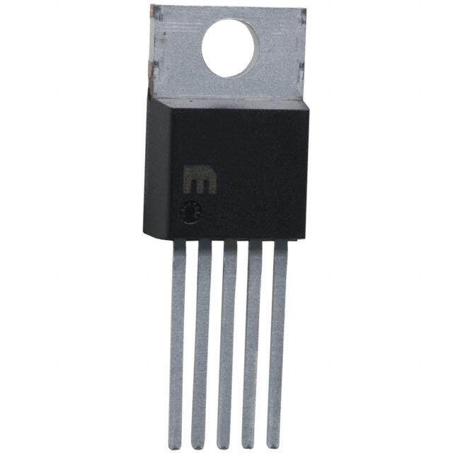
| 描述 | IC REG LDO 3.3V 1A 8SON低压差稳压器 1A LDO with reverse battery protection |
| 产品分类 | |
| 品牌 | Texas Instruments |
| 产品手册 | |
| 产品图片 |
|
| rohs | 符合RoHS无铅 / 符合限制有害物质指令(RoHS)规范要求 |
| 产品系列 | 电源管理 IC,低压差稳压器,Texas Instruments TPS73733QDRBRQ1- |
| 数据手册 | |
| 产品型号 | TPS73733QDRBRQ1 |
| PCN设计/规格 | |
| 产品目录页面 | |
| 产品种类 | 低压差稳压器 |
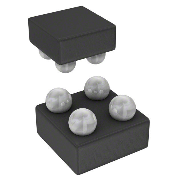
| 供应商器件封装 | 8-SON 裸露焊盘(3x3) |
| 其它名称 | 296-24157-1 |
| 包装 | 剪切带 (CT) |
| 单位重量 | 24 mg |
| 商标 | Texas Instruments |
| 回动电压—最大值 | 500 mV at 1 A |
| 安装类型 | 表面贴装 |
| 安装风格 | SMD/SMT |
| 封装 | Reel |
| 封装/外壳 | 8-VDFN 裸露焊盘 |
| 封装/箱体 | VSON-8 |
| 工作温度 | -40°C ~ 125°C |
| 工厂包装数量 | 3000 |
| 最大功率耗散 | 2.5 W |
| 最大工作温度 | + 125 C |
| 最大输入电压 | 5.5 V |
| 最小工作温度 | - 40 C |
| 最小输入电压 | + 2.2 V |
| 标准包装 | 1 |
| 电压-跌落(典型值) | 0.13V @ 1A |
| 电压-输入 | 最高 5.5V |
| 电压-输出 | 3.3V |
| 电压调节准确度 | 1 % |
| 电流-输出 | 1A |
| 电流-限制(最小值) | 1.05A |
| 稳压器拓扑 | 正,固定式 |
| 稳压器数 | 1 |
| 系列 | TPS73733-Q1 |
| 线路调整率 | 0.01 % / V |
| 负载调节 | 0.002 % / mA |
| 输出电压 | 3.3 V |
| 输出电流 | 1 A |
| 输出端数量 | 1 Output |
| 输出类型 | Fixed |


- 商务部:美国ITC正式对集成电路等产品启动337调查
- 曝三星4nm工艺存在良率问题 高通将骁龙8 Gen1或转产台积电
- 太阳诱电将投资9.5亿元在常州建新厂生产MLCC 预计2023年完工
- 英特尔发布欧洲新工厂建设计划 深化IDM 2.0 战略
- 台积电先进制程称霸业界 有大客户加持明年业绩稳了
- 达到5530亿美元!SIA预计今年全球半导体销售额将创下新高
- 英特尔拟将自动驾驶子公司Mobileye上市 估值或超500亿美元
- 三星加码芯片和SET,合并消费电子和移动部门,撤换高东真等 CEO
- 三星电子宣布重大人事变动 还合并消费电子和移动部门
- 海关总署:前11个月进口集成电路产品价值2.52万亿元 增长14.8%


PDF Datasheet 数据手册内容提取
Product Order Technical Tools & Support & Folder Now Documents Software Community TPS737-Q1 SBVS123B–DECEMBER2008–REVISEDSEPTEMBER2019 TPS737-Q1 1-A Low-Dropout Regulator With Reverse Current Protection 1 Features 2 Applications • Qualifiedforautomotiveapplications • PointofloadregulationforDSPs,FPGAs,ASICs, 1 • AEC-Q100qualifiedwiththefollowingresults: andmicroprocessors – Devicetemperaturegrade1: –40°Cto125°C • Post-regulationforswitchingsupplies ambientoperatingtemperaturerange • Portableandbattery-poweredequipment – DeviceHBMESDclassificationlevel2 3 Description – DeviceCDMESDclassificationlevelC4A The TPS737xx-Q1 family of linear low-dropout (LDO) • Stablewith1-µForlargerceramicoutput voltage regulators uses an NMOS pass element in a capacitor voltage-follower configuration. This topology is • Inputvoltagerange:2.2Vto5.5V relatively insensitive to output capacitor value and • Ultra-lowdropoutvoltage:130mV(typical)at1A ESR, allowing a wide variety of load configurations. Load transient response is excellent, even with a • Excellentloadtransientresponse,evenwithonly small 1-µF ceramic output capacitor. The NMOS 1-µFoutputcapacitor topologyalsoallowsverylowdropout. • NMOStopologydeliverslowreverseleakage The TPS737xx-Q1 family uses an advanced BiCMOS current process to yield high precision while delivering very • 1%initialaccuracy low dropout voltages and low ground pin current. • 3%overallaccuracyoverline,load,and Current consumption, when not enabled, is under temperature 20 nA and ideal for portable applications. These devices are protected by thermal shutdown and • Lessthan20-nA(typical)quiescentcurrentin foldbackcurrentlimit. shutdownmode • Thermalshutdownandcurrentlimitforfault DeviceInformation(1) protection PARTNUMBER PACKAGE BODYSIZE(NOM) • Availableinmultipleoutputvoltageversions TPS737-Q1 VSON(8) 3.00mm×3.00mm (1) For all available packages, see the orderable addendum at theendofthedatasheet. TypicalApplicationCircuit VIN IN OUT VOUT TPS737xx EN GND ON OFF 1 An IMPORTANT NOTICE at the end of this data sheet addresses availability, warranty, changes, use in safety-critical applications, intellectualpropertymattersandotherimportantdisclaimers.PRODUCTIONDATA.
TPS737-Q1 SBVS123B–DECEMBER2008–REVISEDSEPTEMBER2019 www.ti.com Table of Contents 1 Features.................................................................. 1 8 ApplicationandImplementation........................ 14 2 Applications........................................................... 1 8.1 ApplicationInformation............................................14 3 Description............................................................. 1 8.2 TypicalApplication..................................................14 4 RevisionHistory..................................................... 2 9 PowerSupplyRecommendations...................... 16 5 PinConfigurationandFunctions......................... 3 10 Layout................................................................... 16 6 Specifications......................................................... 4 10.1 LayoutGuidelines.................................................16 6.1 AbsoluteMaximumRatings......................................4 10.2 LayoutExample....................................................17 6.2 ESDRatings..............................................................4 11 DeviceandDocumentationSupport................. 18 6.3 RecommendedOperatingConditions.......................4 11.1 DocumentationSupport........................................18 6.4 ThermalInformation..................................................4 11.2 ReceivingNotificationofDocumentationUpdates18 6.5 ElectricalCharacteristics...........................................5 11.3 CommunityResources..........................................18 6.6 TypicalCharacteristics..............................................6 11.4 Trademarks...........................................................18 7 DetailedDescription............................................ 11 11.5 ElectrostaticDischargeCaution............................18 7.1 Overview.................................................................11 11.6 Glossary................................................................18 7.2 FunctionalBlockDiagrams.....................................11 12 Mechanical,Packaging,andOrderable Information........................................................... 18 7.3 FeatureDescription.................................................12 12.1 PackageMounting................................................18 7.4 DeviceFunctionalModes........................................13 4 Revision History NOTE:Pagenumbersforpreviousrevisionsmaydifferfrompagenumbersinthecurrentversion. ChangesfromRevisionA(July2016)toRevisionB Page • ChangeddevicetemperaturegradeAEC-Q100Featuresbullet............................................................................................ 1 • Deletedsub-bulletsfromFeaturesoutputvoltageversionbullet .......................................................................................... 1 ChangesfromOriginal(December2008)toRevisionA Page • AddedDeviceInformationtable,PinConfigurationandFunctionssection,Specificationssection,ESDRatingstable, RecommendedOperatingConditionstable,ThermalInformationtable,DetailedDescriptionsection,Applicationand Implementationsection,PowerSupplyRecommendationssection,Layoutsection,DeviceandDocumentation Supportsection,andMechanical,Packaging,andOrderableInformationsection................................................................ 1 • DeletedOrderingInformationTable;seePOAattheendofthedatasheet.......................................................................... 1 2 SubmitDocumentationFeedback Copyright©2008–2019,TexasInstrumentsIncorporated ProductFolderLinks:TPS737-Q1
TPS737-Q1 www.ti.com SBVS123B–DECEMBER2008–REVISEDSEPTEMBER2019 5 Pin Configuration and Functions DRBPackage 8-PinVSON TopView OUT 1 8 IN NC 2 7 NC Pad FB,NR 3 6 NC GND 4 5 EN Not to scale PinFunctions PIN I/O DESCRIPTION NAME NO. Drivingtheenablepin(EN)highturnsontheregulator.Drivingthispinlowputstheregulatorinto EN 5 I shutdownmode.SeeEnablePinandShutdownformoredetails.ENmustnotbeleftfloatingandcanbe connectedtoINifnotused. Adjustablevoltageversiononly.Thisistheinputtothecontrollooperroramplifier,anditisusedtoset FB 3 I theoutputvoltageofthedevice. GND 4,Pad G Ground IN 8 I Unregulatedinputsupply Fixedvoltageversionsonly.Connectinganexternalcapacitortothispinbypassesnoisegeneratedby NR 3 — theinternalbandgap,reducingoutputnoisetoverylowlevels. OUT 1 O Regulatoroutput.A1-µForlargercapacitorofanytypeisrequiredforstability. NC 2,6,7 — Nointernalconnection Copyright©2008–2019,TexasInstrumentsIncorporated SubmitDocumentationFeedback 3 ProductFolderLinks:TPS737-Q1
TPS737-Q1 SBVS123B–DECEMBER2008–REVISEDSEPTEMBER2019 www.ti.com 6 Specifications 6.1 Absolute Maximum Ratings overoperatingfree-airtemperaturerange(unlessotherwisenoted)(1) MIN MAX UNIT Inputsupplyvoltage –0.3 6 V Enablevoltage –0.3 6 V Outputvoltage –0.3 5.5 V Inputvoltage NRorFBpin –0.3 6 V Peakoutputcurrent Internallylimited Outputshort-circuitduration Indefinite Junctiontemperaturerange,T –55 150 °C J Storagetemperature,T –65 150 °C stg (1) StressesbeyondthoselistedunderAbsoluteMaximumRatingsmaycausepermanentdamagetothedevice.Thesearestressratings only,whichdonotimplyfunctionaloperationofthedeviceattheseoranyotherconditionsbeyondthoseindicatedunderRecommended OperatingConditions.Exposuretoabsolute-maximum-ratedconditionsforextendedperiodsmayaffectdevicereliability. 6.2 ESD Ratings VALUE UNIT Human-bodymodel(HBM),perAECQ100-002(1) ±2000 V Electrostaticdischarge V (ESD) Charged-devicemodel(CDM),perAECQ100-011 ±500 (1) AECQ100-002indicatesthatHBMstressingshallbeinaccordancewiththeANSI/ESDA/JEDECJS-001specification. 6.3 Recommended Operating Conditions overoperatingfree-airtemperaturerange(unlessotherwisenoted) MIN MAX UNIT V Inputsupplyvoltage 2.2 5.5 V IN I Outputcurrent 0 1 A OUT T Operatingjunctiontemperature –40 125 °C J 6.4 Thermal Information TPS737xx-Q1 THERMALMETRIC(1) DRB(VSON) UNIT 8PINS R Junction-to-ambientthermalresistance 52.2 °C/W θJA R Junction-to-case(top)thermalresistance 59.4 °C/W θJC(top) R Junction-to-boardthermalresistance 19.3 °C/W θJB ψ Junction-to-topcharacterizationparameter 2 °C/W JT ψ Junction-to-boardcharacterizationparameter 19.3 °C/W JB R Junction-to-case(bottom)thermalresistance 11.8 °C/W θJC(bot) (1) Formoreinformationabouttraditionalandnewthermalmetrics,seetheSemiconductorandICPackageThermalMetricsapplication report. 4 SubmitDocumentationFeedback Copyright©2008–2019,TexasInstrumentsIncorporated ProductFolderLinks:TPS737-Q1
TPS737-Q1 www.ti.com SBVS123B–DECEMBER2008–REVISEDSEPTEMBER2019 6.5 Electrical Characteristics overoperatingtemperaturerange(T =–40°Cto125°C),V =(V +1V)(1),I =10mA,V =2.2V,C =2.2µF J IN OUT(nom) OUT EN OUT (unlessotherwisenoted).TypicalvaluesareatT =25°C. J PARAMETER TESTCONDITIONS MIN TYP MAX UNIT V Inputvoltagerange(1)(2) 2.2 5.5 V IN V Internalreference(TPS73701) T =25°C 1.192 1.2 1.216 V FB J Outputvoltagerange(TPS73701)(3) V 5.5–V V FB DO Nominal T =25°C –1 1 J 5.36V<V <5.5V,V =5.08V, IN OUT VOUT Accuracy(1)(4) 10mA<IOUT<800mA, –2 2 % –40°C<T <85°C,TPS73701 J OverV ,I ,and V +0.5V≤V ≤5.5V, IN OUT OUT IN –3 ±0.5 3 temperature 10mA≤I ≤1A OUT ΔV %/ΔV Lineregulation(1) V +0.5V≤V ≤5.5V 0.01 %/V OUT IN OUT(nom) IN 1mA≤I ≤1A 0.002 OUT ΔV %/ΔI Loadregulation %/mA OUT OUT 10mA≤I ≤1A 0.0005 OUT Dropoutvoltage(5) V I =1A 130 500 mV DO (V =V –0.1V) OUT IN OUT(nom) Z (DO) Outputimpedanceindropout 2.2V≤V ≤V +V 0.25 Ω O IN OUT DO I Outputcurrentlimit V =0.9×V 1.05 1.6 2.2 A CL OUT OUT(nom) I Short-circuitcurrent V =0V 450 mA SC OUT I Reverseleakagecurrent(6)(–I ) V ≤0.5V,0V≤V ≤V 0.1 µA REV IN EN IN OUT I =10mA(I ) 400 OUT Q I GNDpincurrent µA GND I =1A 1300 OUT I Shutdowncurrent(I ) V ≤0.5V,V ≤V ≤5.5V 20 nA SHDN GND EN OUT IN I FBpincurrent(TPS73701) 0.1 0.6 µA FB Power-supplyrejectionratio f=100Hz,IOUT=1A 58 PSRR dB (ripplerejection) f=10kHz,I =1A 37 OUT Outputnoisevoltage V C =10µF 27×V µV N BW=10Hzto100kHz OUT OUT RMS t Startuptime V =3V,R =30Ω,C =1µF 600 µs STR OUT L OUT V ENpinhigh(enabled) 1.7 V V EN(HI) IN V ENpinlow(shutdown) 0 0.5 V EN(LO) I ENpincurrent(enabled) V =5.5V 20 nA EN(HI) EN Shutdown,temperatureincreasing 160 T Thermalshutdowntemperature °C SD Reset,temperaturedecreasing 140 T Operatingjunctiontemperature –40 125 °C J (1) MinimumV =V +V or2.2V,whicheverisgreater. IN OUT DO (2) ForV <1.6V,whenV ≤1.6V,theoutputlockstoV andmayresultinanovervoltageconditionontheoutput.Toavoidthis OUT(nom) IN IN situation,disablethedevicebeforepoweringdownV . IN (3) TPS73701istestedatV =1.2V. OUT (4) Toleranceofexternalresistorsnotincludedinthisspecification. (5) V isnotmeasuredforfixedoutputversionswithV <2.3V,becauseminimumV =2.2V. DO OUT(nom) IN (6) Fixed-voltageversionsonly;seetheReverseCurrentsectionformoreinformation. Copyright©2008–2019,TexasInstrumentsIncorporated SubmitDocumentationFeedback 5 ProductFolderLinks:TPS737-Q1
TPS737-Q1 SBVS123B–DECEMBER2008–REVISEDSEPTEMBER2019 www.ti.com 6.6 Typical Characteristics T =25°C,V =(V +1V),I =10mA,V =2.2V,C =2.2µF(unlessotherwisenoted) J IN OUT(nom) OUT EN OUT 0.5 0.20 0.4 Referred to IOUT= 10mA Referred to VIN= VOUT+ 1.0V at IOUT= 10mA 0.15 0.3 -40°C +25°C 0.10 (%)UT 00..21 +125°C (%)UT 0.05 +125°C +25°C O O V V n 0 n 0 nge i -0.1 nge i -0.05 ha -0.2 ha -40°C C C -0.10 -0.3 -0.4 -0.15 -0.5 -0.20 0 100 200 300 400 500 600 700 800 900 1000 0 0.5 1.0 1.5 2.0 2.5 3.0 3.5 4.0 4.5 I (mA) V -V (V) OUT IN OUT Figure1.LoadRegulation Figure2.LineRegulation 200 200 V = 2.5V 180 OUT 180 160 160 +125°C +25°C 140 140 V) 120 V) 120 m m ( 100 ( 100 O O VD 80 VD 80 60 60 -40°C 40 40 20 20 0 0 0 100 200 300 400 500 600 700 800 900 1000 -50 -25 0 25 50 75 100 125 150 I (mA) Temperature (°C) OUT Figure3.DropoutVoltagevsOutputCurrent Figure4.DropoutVoltagevsTemperature 30 18 I = 10mA I = 10mA OUT OUT 16 25 14 %) %) Units ( 20 Units ( 1120 nt of 15 nt of 8 e e erc 10 erc 6 P P 4 5 2 0 0 -1.0-0.9-0.8-0.7-0.6-0.5-0.4-0.3-0.2-0.100.10.20.30.40.50.60.70.80.91.0 -100-90-80-70-60-50-40-30-20-100102030405060708090100 V Error(%) Worst Case dV /dT (ppm/°C) OUT OUT Figure5.OutputVoltageHistogram Figure6.DropoutVoltageDriftHistogram 6 SubmitDocumentationFeedback Copyright©2008–2019,TexasInstrumentsIncorporated ProductFolderLinks:TPS737-Q1
TPS737-Q1 www.ti.com SBVS123B–DECEMBER2008–REVISEDSEPTEMBER2019 Typical Characteristics (continued) T =25°C,V =(V +1V),I =10mA,V =2.2V,C =2.2µF(unlessotherwisenoted) J IN OUT(nom) OUT EN OUT 2500 3000 I = 1A OUT V = 5.0V IN 2500 2000 V = 5.0V IN 2000 A) A) 1500 (m V = 3.3V (mND VIN= 3.3V IGND 1500 IN IG 1000 1000 VIN= 2.2V VIN= 2.2V 500 500 0 0 0 200 400 600 800 1000 -50 -25 0 25 50 75 100 125 I (mA) Temperature (°C) OUT Figure7.GroundPinCurrentvsOutputCurrent Figure8.GroundPinCurrentvsTemperature 1 2.0 V = 0.5V ENABLE 1.8 VIN= VOUT+ 0.5V 1.6 ICL A) 1.4 m (mA) 0.1 Limit ( 11..20 GND ent 0.8 I Curr 0.6 I 0.4 SC 0.2 V = 3.3V 0 OUT 0.01 0 0.5 1.0 1.5 2.0 2.5 3.0 3.5 -50 -25 0 25 50 75 100 125 V (V) Temperature(°C) OUT Figure9.GroundPinCurrentInShutdownvsTemperature Figure10.CurrentLimitvsVOUT(Foldback) 2.0 2.0 V = 1.2V 1.9 1.9 OUT 1.8 1.8 A) 1.7 A) 1.7 mit ( 1.6 mit ( 1.6 Li 1.5 Li 1.5 nt nt urre 1.4 urre 1.4 C 1.3 C 1.3 1.2 1.2 1.1 1.1 1.0 1.0 2.0 2.5 3.0 3.5 4.0 4.5 5.0 5.5 -50 -25 0 25 50 75 100 125 V (V) Temperature (°C) IN Figure11.CurrentLimitvsV Figure12.CurrentLimitvsTemperature IN Copyright©2008–2019,TexasInstrumentsIncorporated SubmitDocumentationFeedback 7 ProductFolderLinks:TPS737-Q1
TPS737-Q1 SBVS123B–DECEMBER2008–REVISEDSEPTEMBER2019 www.ti.com Typical Characteristics (continued) T =25°C,V =(V +1V),I =10mA,V =2.2V,C =2.2µF(unlessotherwisenoted) J IN OUT(nom) OUT EN OUT 90 40 I = 100mA I = 1mA 80 COUT = Any COUT = 1mF 35 OUT OUT 70 B) IOUT= 1mA 30 e Rejection (d 654000 ICOOUUTT== 1 AmnAy COUT= 10mF IOC= O10=0 1mmAF PSRR (dB) 221505 pl 30 Rip 10 Frequency = 10kHz 20 IOUT= 100mA COUT= 10mF C = 10mF 10 OUT 5 VOUT= 2.5V I = 100mA 0 0 OUT 10 100 1k 10k 100k 1M 10M 0 0.2 0.4 0.6 0.8 1.0 1.2 1.4 1.6 1.8 2.0 Frequency (Hz) VIN-VOUT(V) Figure13.PSRR(RippleRejection)vsFrequency Figure14.PSRR(RippleRejection)vsV –V IN OUT 1 60 C = 1mF 55 OUT 50 Hz) S) 45 Ö M V/ 0.1 R 40 m C = 10mF ( ( OUT N eN V 35 V = 2.5V 30 OUT C = 0mF OUT 25 R1= 39.2kW IOUT= 150mA 10Hz < Frequency < 100kHz 0.01 20 10 100 1k 10k 100k 10p 100p 1n 10n Frequency (Hz) C (F) FB Figure15.NoiseSpectralDensity Figure16.TPS73701RMSNoiseVoltagevsC FB 60 140 V =5.0V OUT 50 120 V =5.0V OUT 100 40 MS) MS) 80 VOUT=3.3V (RN 30 VOUT=3.3V (RN 60 V V 20 40 V =1.5V V =1.5V OUT OUT 10 20 CNR=0.01mF COUT=0mF 10Hz<Frequency<100kHz 10Hz<Frequency<100kHz 0 0 0.1 1 10 1p 10p 100p 1n 10n C (mF) C (F) OUT NR Figure17.RMSNoiseVoltagevsC Figure18.RMSNoiseVoltagevsC OUT NR 8 SubmitDocumentationFeedback Copyright©2008–2019,TexasInstrumentsIncorporated ProductFolderLinks:TPS737-Q1
TPS737-Q1 www.ti.com SBVS123B–DECEMBER2008–REVISEDSEPTEMBER2019 Typical Characteristics (continued) T =25°C,V =(V +1V),I =10mA,V =2.2V,C =2.2µF(unlessotherwisenoted) J IN OUT(nom) OUT EN OUT C = 10nF C = 10nF NR NR COUT= 10mF V 200mV/div OUT COUT= 10mF 100mV/div V OUT 1A 5.3V 10mA 4.3V IOUT VIN 10ms/div 10ms/div Figure19.TPS73733LoadTransientResponse Figure20.TPS73733LineTransientResponse V RL= 20W OUT COUT= 10mF 1V/div RCLOU=T 2=0 1WmF 1V/div RCLOU=T 2=0 1WmF RL= 20W COUT= 10mF V OUT 2V 2V V EN 1V/div 1V/div 0V 0V V EN 100ms/div 100ms/div Figure21.TPS73701Turn-OnResponse Figure22.TPS73701Turn-OffResponse 10 6 5 VIN 4 V OUT 1 3 A) n ( Volts 2 NABLE 1 IE0.1 0 -1 -2 0.01 -50 -25 0 25 50 75 100 125 50ms/div Temperature(°C) Figure23.TPS73701,VOUT=3.3V Figure24.IENABLEvsTemperature Power-UpAndPower-Down Copyright©2008–2019,TexasInstrumentsIncorporated SubmitDocumentationFeedback 9 ProductFolderLinks:TPS737-Q1
TPS737-Q1 SBVS123B–DECEMBER2008–REVISEDSEPTEMBER2019 www.ti.com Typical Characteristics (continued) T =25°C,V =(V +1V),I =10mA,V =2.2V,C =2.2µF(unlessotherwisenoted) J IN OUT(nom) OUT EN OUT 160 160 140 140 120 120 100 100 A) A) (n 80 (n 80 B B IF 60 IF 60 40 40 20 20 0 0 -50 -25 0 25 50 75 100 125 −50 −25 0 25 50 75 100 125 Temperature (°C) Temperature (°C) Figure25.TPS73701IFBvsTemperature Figure26.TPS73701IFBvsTemperature C = 10nF V = 2.5V FB OUT 100mV/div R1= 39.2kW COUT= 10mF VOUT 100mV/div COUT= 10mF CFB= 10nF VOUT 4.5V 250mA 3.5V I V OUT IN 10mA 10ms/div 5ms/div Figure27.TPS73701LoadTransient,AdjustableVersion Figure28.TPS73701LineTransient,AdjustableVersion 10 SubmitDocumentationFeedback Copyright©2008–2019,TexasInstrumentsIncorporated ProductFolderLinks:TPS737-Q1
TPS737-Q1 www.ti.com SBVS123B–DECEMBER2008–REVISEDSEPTEMBER2019 7 Detailed Description 7.1 Overview The TPS737xx-Q1 belongs to a family of new generation LDO regulators that use an NMOS pass transistor to achieve ultra-low-dropout performance, reverse current blockage, and freedom from output capacitor constraints. These features combined with an enable input make the TPS737xx-Q1 ideal for portable applications. This regulator family offers a wide selection of fixed output voltage versions and an adjustable output version. All versionshavethermalandover-currentprotection,includingfoldbackcurrentlimit. Table1.Standard1%ResistorValuesforCommon OutputVoltages V R R OUT 1 2 1.2V Short Open 1.5V 23.2kΩ 95.3kΩ 1.8V 28.kΩ 56.2kΩ 2.5V 39.2kΩ 36.5kΩ 2.8V 44.2kΩ 33.2kΩ 3V 46.4kΩ 33.2kΩ 3.3V 52.3kΩ 30.1kΩ 7.2 Functional Block Diagrams IN 4-MHz ChargePump EN Thermal Protection Ref Servo 27 kW Bandgap Error Amp Current Limit OUT GND 8 kW R1 R1+R2=80 kW R2 NR Figure29. FixedVoltageVersion Copyright©2008–2019,TexasInstrumentsIncorporated SubmitDocumentationFeedback 11 ProductFolderLinks:TPS737-Q1
TPS737-Q1 SBVS123B–DECEMBER2008–REVISEDSEPTEMBER2019 www.ti.com Functional Block Diagrams (continued) IN 4-MHz ChargePump EN Thermal Protection Ref Servo 27 kW Bandgap Error Amp Current OUT Limit GND 8 kW 80 kW R1 FB R2 SeeTable1forstandardresistorvalues. Figure30. AdjustableVoltageVersion 7.3 Feature Description 7.3.1 OutputNoise A precision bandgap reference is used to generate the internal reference voltage (V ). This reference is the REF dominant noise source within the TPS737xx-Q1 and it generates approximately 32 µV (10 Hz to 100 kHz) at RMS the reference output (NR). The regulator control loop adds gain to the reference noise with the same gain as the referencevoltage,sothatthenoisevoltageoftheregulatorisapproximatelygivenbyEquation1. (R +R ) V V =32µV ´ 1 2 =32µV ´ OUT N RMS RMS R V 2 REF (1) BecausethevalueofV is1.2V,thisrelationshipreducesto: REF æµV ö VN(µVRMS)=27ç RMS ÷´VOUT(V) è V ø (2) forthecaseofnoC . NR An internal 27-kΩ resistor in series with the noise reduction pin (NR) forms a low-pass filter for the voltage reference when an external noise reduction capacitor (C ) is connected from NR to ground. The total noise in NR the 10-Hz to 100-kHz bandwidth is reduced by a factor of approximately 3.2 for C = 10 nF, giving the NR approximaterelationshipforC =10nFinEquation3. NR æµV ö V (µV )=8.5ç RMS ÷´V (V) N RMS OUT è V ø (3) ThisnoisereductioneffectisshowninFigure18. TheTPS737xx-Q1usesaninternalchargepump to develop an internal supply voltage sufficient to drive the gate of the NMOS pass element above V . The charge pump generates approximately 250 µV of switching noise at OUT approximately 4 MHz, however, charge-pump noise contribution is negligible at the output of the regulator for mostvaluesofI andC . OUT OUT 12 SubmitDocumentationFeedback Copyright©2008–2019,TexasInstrumentsIncorporated ProductFolderLinks:TPS737-Q1
TPS737-Q1 www.ti.com SBVS123B–DECEMBER2008–REVISEDSEPTEMBER2019 Feature Description (continued) 7.3.2 InternalCurrentLimit The TPS737xx-Q1 internal current limit helps protect the regulator during fault conditions. Foldback current limit helps to protect the regulator from damage during output short-circuit conditions by reducing current limit when V dropsbelow0.5V.SeeFigure10. OUT 7.3.3 EnablePinandShutdown The enable pin (EN) is active high and is compatible with standard TTL-CMOS levels. A V below 0.5 V EN (maximum) turns the regulator off and drops the GND pin current to approximately 10 nA. When EN is used to shutdown the regulator, all charge is removed from the pass transistor gate, and the output ramps back up to a regulatedV (seeFigure21). OUT When shutdown capability is not required, EN can be connected to V . However, the pass gate may not be IN discharged using this configuration, and the pass transistor may be left on (enhanced) for a significant time after V is removed. This scenario can result in reverse current flow (if the IN pin is low impedance) and faster ramp IN times upon power-up. In addition, for V ramp times slower than a few milliseconds, the output may overshoot IN uponpower-up. 7.3.4 ReverseCurrent The NMOS pass element of the TPS737xx-Q1 provides inherent protection against current flow from the output of the regulator to the input when the gate of the pass device is pulled low. To ensure that all charge is removed from the gate of the pass element, the EN pin must be driven low before the input voltage is removed. If this is notdone,thepasselementmaybeleftonbecauseofstoredchargeonthegate. After the EN pin is driven low, no bias voltage is required on any pin for reverse current blocking. Reverse current is specified as the current flowing out of the IN pin because of voltage applied on the OUT pin. There is additional current flowing into the OUT pin as a result of the 80-kΩ internal resistor divider to ground (see Figure29andFigure30). FortheTPS73701,reversecurrentmayflowwhenV ismorethan1VaboveV . FB IN 7.3.5 ThermalProtection Thermal protection disables the output when the junction temperature rises to approximately 160°C, allowing the device to cool. When the junction temperature cools to approximately 140°C, the output circuitry is again enabled. Depending on power dissipation, thermal resistance, and ambient temperature, the thermal protection circuit may cycle on and off. This cycling limits the dissipation of the regulator, protecting it from damage due to overheating. Any tendency to activate the thermal protection circuit indicates excessive power dissipation or an inadequate heatsink. Junction temperature must be limited to 125°C maximum for reliable operation. To estimate the margin of safety in a complete design (including heatsink), increase the ambient temperature until the thermal protection is triggered; use worst-case loads and signal conditions. Thermal protection must trigger at least 35°C above the maximum expected ambient condition of your application for good reliability. This produces a worst-case junction temperatureof125°Catthehighestexpectedambienttemperatureandworst-caseload. TheinternalprotectioncircuitryoftheTPS737xx-Q1isdesignedtoprotectagainstoverloadconditions.It was not intended to replace proper heatsinking. Continuously running the TPS737xx-Q1 into thermal shutdown degrades devicereliability. 7.4 Device Functional Modes Driving the EN pin over 1.7 V turns on the regulator. Driving the EN below 0.5 V causes the regulator to enter shutdownmode.Inshutdwon,thecurrentconsumptionofthedeviceisreducedto20nA(typical). Copyright©2008–2019,TexasInstrumentsIncorporated SubmitDocumentationFeedback 13 ProductFolderLinks:TPS737-Q1
TPS737-Q1 SBVS123B–DECEMBER2008–REVISEDSEPTEMBER2019 www.ti.com 8 Application and Implementation NOTE Information in the following applications sections is not part of the TI component specification, and TI does not warrant its accuracy or completeness. TI’s customers are responsible for determining suitability of components for their purposes. Customers should validateandtesttheirdesignimplementationtoconfirmsystemfunctionality. 8.1 Application Information The TPS737xx-Q1 family of LDO regulators use an NMOS pass transistor to achieve ultra-low-dropout performance, reverse current blockage, and freedom from output capacitor constraints. These features, combinedwithlownoiseandanenableinput,maketheTPS737xx-Q1idealforportableapplications. 8.2 Typical Application VIN IN OUT VOUT TPS737xx EN GND ON OFF Figure31. TypicalApplicationCircuitForFixed-VoltageVersions Optional input capacitor. Optional output capacitor. May improve source May improve load transient, impedance, noise, or PSRR. noise, or PSRR. VIN IN OUT VOUT TPS73701 R C 1 FB EN GND FB ON R OFF 2 (R +R) Optional capacitor V = 1 2 x 1.204 reduces output noise OUT R2 and improves transient response. Figure32. TypicalApplicationCircuitForAdjustable-VoltageVersion 8.2.1 DesignRequirements R and R can be calculated for any output voltage using the formula shown in Figure 32. Sample resistor values 1 2 forcommonoutputvoltagesareshowninTable1. Make the parallel combination of R and R approximately equal to 19 kΩ for best accuracy. This 19 kΩ, in 1 2 addition to the internal 8-kΩ resistor, presents the same impedance to the error amplifier as the 27-kΩ bandgap referenceoutput.Thisimpedancehelpscompensateforleakagesintotheerroramplifierterminals. The TPS73701 adjustable version does not have the NR pin available. However, connecting a feedback capacitor (C ) from the output to the feedback pin (FB) reduces output noise and improves load transient FB performance.Thiscapacitormustbelimitedto0.1µF. 14 SubmitDocumentationFeedback Copyright©2008–2019,TexasInstrumentsIncorporated ProductFolderLinks:TPS737-Q1
TPS737-Q1 www.ti.com SBVS123B–DECEMBER2008–REVISEDSEPTEMBER2019 Typical Application (continued) 8.2.2 DetailedDesignProcedure 8.2.2.1 InputandOutputCapacitorRequirements Although an input capacitor is not required for stability, if input impedance is very low, it is good analog design practice to connect a 0.1-µF to 1-µF low equivalent series resistance (ESR) capacitor across the input supply near the regulator. This capacitor counteracts reactive input sources and improves transient response, noise rejection, and ripple rejection. A higher-value capacitor may be necessary if large, fast rise-time load transients areanticipatedorthedeviceislocatedseveralinchesfromthepowersource. The TPS737xx-Q1 requires a 1-µF output capacitor for stability. It is designed to be stable for all available types and values of capacitors. In applications where multiple low ESR capacitors are in parallel, ringing may occur when the product of C and total ESR drops below 50 nΩF. Total ESR includes all parasitic resistances, OUT includingcapacitorESRandboard,socket,andsolderjoint resistance. In most applications, the sum of capacitor ESRandtraceresistancemeetsthisrequirement. 8.2.2.2 DropoutVoltage The TPS737xx-Q1 uses an NMOS pass transistor to achieve extremely low dropout. When (V – V ) is less IN OUT than the dropout voltage (V ), the NMOS pass device is in its linear region of operation and the input-to-output DO resistanceistheR oftheNMOSpasselement. DS(ON) The TPS737xx-Q1 requires a larger voltage drop from V to V to avoid degraded transient response for large IN OUT step changes in load current. The boundary of this transient dropout region is approximately twice the DC dropout.ValuesofV –V abovethislineensurenormaltransientresponse. IN OUT Operating in the transient dropout region can cause an increase in recovery time. The time required to recover from a load transient is a function of the magnitude of the change in load current rate, the rate of change in load current, and the available headroom (V to V voltage drop). Under worst-case conditions (full-scale IN OUT instantaneous load change with (V – V ) close to DC dropout levels), the TPS737xx-Q1 can take a couple of IN OUT hundredmicrosecondstoreturntothespecifiedregulationaccuracy. 8.2.2.3 TransientResponse The low open-loop output impedance provided by the NMOS pass element in a voltage follower configuration allows operation without a 1-µF output capacitor. As with any regulator, the addition of additional capacitance from the OUT pin to ground reduces undershoot magnitude but increases its duration. In the adjustable version, theadditionofacapacitor(C )betweentheOUTpinandtheFBpinalsoimprovesthetransientresponse. FB The TPS737xx-Q1 does not have active pulldown when the output is overvoltage. This architecture allows for applications that connect higher voltage sources, such as alternate power supplies, to be connected to the output. This architecture also results in an output overshoot of several percent if the load current quickly drops to zero when a capacitor is connected to the output. The duration of overshoot can be reduced by adding a load resistor. The overshoot decays at a rate determined by the output capacitor (C ) and the internal and external OUT loadresistance.TherateofdecayisgivenbyEquation4 andEquation5. (Fixedvoltageversion) dV V = OUT dT C ´80kWPR OUT LOAD (4) (Adjustablevoltageversion) dV V OUT = dT C ´80kWP(R +R )PR OUT 1 2 LOAD (5) Copyright©2008–2019,TexasInstrumentsIncorporated SubmitDocumentationFeedback 15 ProductFolderLinks:TPS737-Q1
TPS737-Q1 SBVS123B–DECEMBER2008–REVISEDSEPTEMBER2019 www.ti.com Typical Application (continued) 8.2.3 ApplicationCurves Figure33.TPS737xx-Q1Start-Up Figure34.TPS737xx-Q1Shutdown 9 Power Supply Recommendations The device is designed to operate from an input voltage supply range from 2.2 V to 5.5 V. The input voltage range provides adequate headroom for the device to have a regulated output. This input supply must be well regulated. If the input supply is noisy, additional input capacitors with low ESR help improve the output noise performance. 10 Layout 10.1 Layout Guidelines 10.1.1 ImprovePSRRandNoisePerformance TI recommends that the printed circuit board (PCB) be designed with separate ground planes for V and V , IN OUT with each ground plane connected only at the GND pin of the device, to improve AC performance such as PSRR, output noise, and transient response. In addition, the ground connection for the bypass capacitor must connectdirectlytotheGNDpinofthedevice. 10.1.2 PowerDissipation The ability to remove heat from the die is different for each package type, presenting different considerations in the PCB layout. The PCB area around the device that is free of other components moves the heat from the device to the ambient air. Performance data for JEDEC low-K and high-K boards are shown in Thermal Information. Using heavier copper increases the effectiveness in removing heat from the device. The addition of platedthrough-holestoheat-dissipatinglayersalsoimprovestheheatsinkeffectiveness. Powerdissipationdependsoninputvoltageandload conditions. Power dissipation (P ) is equal to the product of D theoutputcurrentmultipliedbythevoltagedropacrosstheoutputpasselement(V toV ).SeeEquation6. IN OUT P =(V -V )´I D IN OUT OUT (6) Power dissipation can be minimized by using the lowest possible input voltage necessary to assure the required outputvoltage. 16 SubmitDocumentationFeedback Copyright©2008–2019,TexasInstrumentsIncorporated ProductFolderLinks:TPS737-Q1
TPS737-Q1 www.ti.com SBVS123B–DECEMBER2008–REVISEDSEPTEMBER2019 10.2 Layout Example GND PLANE COUT VOUT VIN TPS737xx-Q1 1 8 C R FF 1 CIN NR/FB 3 6 NC R 2 4 5 EN GND PLANE Figure35. LayoutDiagram Copyright©2008–2019,TexasInstrumentsIncorporated SubmitDocumentationFeedback 17 ProductFolderLinks:TPS737-Q1
TPS737-Q1 SBVS123B–DECEMBER2008–REVISEDSEPTEMBER2019 www.ti.com 11 Device and Documentation Support 11.1 Documentation Support 11.1.1 RelatedDocumentation Forrelateddocumentationseethefollowing: SolderPadRecommendationsforSurface-MountDevices (SBFA015) 11.2 Receiving Notification of Documentation Updates To receive notification of documentation updates, navigate to the device product folder on ti.com. In the upper right corner, click on Alert me to register and receive a weekly digest of any product information that has changed.Forchangedetails,reviewtherevisionhistoryincludedinanyreviseddocument. 11.3 Community Resources TI E2E™ support forums are an engineer's go-to source for fast, verified answers and design help — straight fromtheexperts.Searchexistinganswersoraskyourownquestiontogetthequickdesignhelpyouneed. Linked content is provided "AS IS" by the respective contributors. They do not constitute TI specifications and do notnecessarilyreflectTI'sviews;seeTI'sTermsofUse. 11.4 Trademarks E2EisatrademarkofTexasInstruments. Allothertrademarksarethepropertyoftheirrespectiveowners. 11.5 Electrostatic Discharge Caution This integrated circuit can be damaged by ESD. Texas Instruments recommends that all integrated circuits be handled with appropriateprecautions.Failuretoobserveproperhandlingandinstallationprocedurescancausedamage. ESDdamagecanrangefromsubtleperformancedegradationtocompletedevicefailure.Precisionintegratedcircuitsmaybemore susceptibletodamagebecauseverysmallparametricchangescouldcausethedevicenottomeetitspublishedspecifications. 11.6 Glossary SLYZ022—TIGlossary. Thisglossarylistsandexplainsterms,acronyms,anddefinitions. 12 Mechanical, Packaging, and Orderable Information The following pages include mechanical, packaging, and orderable information. This information is the most current data available for the designated devices. This data is subject to change without notice and revision of thisdocument.Forbrowser-basedversionsofthisdatasheet,refertotheleft-handnavigation. 12.1 Package Mounting See Solder Pad Recommendations for Surface-Mount Devices (SBFA015) for TPS737xx-Q1 solder pad footprint recommendations. 18 SubmitDocumentationFeedback Copyright©2008–2019,TexasInstrumentsIncorporated ProductFolderLinks:TPS737-Q1
PACKAGE OPTION ADDENDUM www.ti.com 6-Feb-2020 PACKAGING INFORMATION Orderable Device Status Package Type Package Pins Package Eco Plan Lead/Ball Finish MSL Peak Temp Op Temp (°C) Device Marking Samples (1) Drawing Qty (2) (6) (3) (4/5) TPS73719QDRBRQ1 ACTIVE SON DRB 8 3000 Green (RoHS NIPDAU Level-3-260C-168 HR -40 to 125 719Q & no Sb/Br) TPS73733QDRBRQ1 ACTIVE SON DRB 8 3000 Green (RoHS NIPDAU Level-3-260C-168 HR -40 to 125 733Q & no Sb/Br) (1) The marketing status values are defined as follows: ACTIVE: Product device recommended for new designs. LIFEBUY: TI has announced that the device will be discontinued, and a lifetime-buy period is in effect. NRND: Not recommended for new designs. Device is in production to support existing customers, but TI does not recommend using this part in a new design. PREVIEW: Device has been announced but is not in production. Samples may or may not be available. OBSOLETE: TI has discontinued the production of the device. (2) RoHS: TI defines "RoHS" to mean semiconductor products that are compliant with the current EU RoHS requirements for all 10 RoHS substances, including the requirement that RoHS substance do not exceed 0.1% by weight in homogeneous materials. Where designed to be soldered at high temperatures, "RoHS" products are suitable for use in specified lead-free processes. TI may reference these types of products as "Pb-Free". RoHS Exempt: TI defines "RoHS Exempt" to mean products that contain lead but are compliant with EU RoHS pursuant to a specific EU RoHS exemption. Green: TI defines "Green" to mean the content of Chlorine (Cl) and Bromine (Br) based flame retardants meet JS709B low halogen requirements of <=1000ppm threshold. Antimony trioxide based flame retardants must also meet the <=1000ppm threshold requirement. (3) MSL, Peak Temp. - The Moisture Sensitivity Level rating according to the JEDEC industry standard classifications, and peak solder temperature. (4) There may be additional marking, which relates to the logo, the lot trace code information, or the environmental category on the device. (5) Multiple Device Markings will be inside parentheses. Only one Device Marking contained in parentheses and separated by a "~" will appear on a device. If a line is indented then it is a continuation of the previous line and the two combined represent the entire Device Marking for that device. (6) Lead/Ball Finish - Orderable Devices may have multiple material finish options. Finish options are separated by a vertical ruled line. Lead/Ball Finish values may wrap to two lines if the finish value exceeds the maximum column width. Important Information and Disclaimer:The information provided on this page represents TI's knowledge and belief as of the date that it is provided. TI bases its knowledge and belief on information provided by third parties, and makes no representation or warranty as to the accuracy of such information. Efforts are underway to better integrate information from third parties. TI has taken and continues to take reasonable steps to provide representative and accurate information but may not have conducted destructive testing or chemical analysis on incoming materials and chemicals. TI and TI suppliers consider certain information to be proprietary, and thus CAS numbers and other limited information may not be available for release. In no event shall TI's liability arising out of such information exceed the total purchase price of the TI part(s) at issue in this document sold by TI to Customer on an annual basis. Addendum-Page 1
PACKAGE OPTION ADDENDUM www.ti.com 6-Feb-2020 OTHER QUALIFIED VERSIONS OF TPS737-Q1 : •Catalog: TPS737 NOTE: Qualified Version Definitions: •Catalog - TI's standard catalog product Addendum-Page 2
PACKAGE MATERIALS INFORMATION www.ti.com 25-Sep-2019 TAPE AND REEL INFORMATION *Alldimensionsarenominal Device Package Package Pins SPQ Reel Reel A0 B0 K0 P1 W Pin1 Type Drawing Diameter Width (mm) (mm) (mm) (mm) (mm) Quadrant (mm) W1(mm) TPS73719QDRBRQ1 SON DRB 8 3000 330.0 12.4 3.3 3.3 1.1 8.0 12.0 Q2 TPS73733QDRBRQ1 SON DRB 8 3000 330.0 12.4 3.3 3.3 1.1 8.0 12.0 Q2 PackMaterials-Page1
PACKAGE MATERIALS INFORMATION www.ti.com 25-Sep-2019 *Alldimensionsarenominal Device PackageType PackageDrawing Pins SPQ Length(mm) Width(mm) Height(mm) TPS73719QDRBRQ1 SON DRB 8 3000 367.0 367.0 35.0 TPS73733QDRBRQ1 SON DRB 8 3000 367.0 367.0 35.0 PackMaterials-Page2
None
PACKAGE OUTLINE DRB0008A VSON - 1 mm max height SCALE 4.000 PLASTIC SMALL OUTLINE - NO LEAD 3.1 B A 2.9 PIN 1 INDEX AREA 3.1 2.9 C 1 MAX SEATING PLANE 0.05 0.08 C DIM A 0.00 OPT 1 OPT 2 1.5 0.1 (0.1) (0.2) 4X (0.23) EXPOSED (DIM A) TYP THERMAL PAD 4 5 2X 1.95 1.75 0.1 8 1 6X 0.65 0.37 8X 0.25 PIN 1 ID 0.1 C A B (OPTIONAL) (0.65) 0.05 C 0.5 8X 0.3 4218875/A 01/2018 NOTES: 1. All linear dimensions are in millimeters. Any dimensions in parenthesis are for reference only. Dimensioning and tolerancing per ASME Y14.5M. 2. This drawing is subject to change without notice. 3. The package thermal pad must be soldered to the printed circuit board for thermal and mechanical performance. www.ti.com
EXAMPLE BOARD LAYOUT DRB0008A VSON - 1 mm max height PLASTIC SMALL OUTLINE - NO LEAD (1.5) (0.65) SYMM 8X (0.6) (0.825) 8X (0.31) 1 8 SYMM (1.75) (0.625) 6X (0.65) 4 5 (R0.05) TYP ( 0.2) VIA TYP (0.23) (0.5) (2.8) LAND PATTERN EXAMPLE EXPOSED METAL SHOWN SCALE:20X 0.07 MAX 0.07 MIN ALL AROUND ALL AROUND EXPOSED EXPOSED METAL METAL SOLDER MASK METAL METAL UNDER SOLDER MASK OPENING SOLDER MASK OPENING NON SOLDER MASK SOLDER MASK DEFINED DEFINED (PREFERRED) SOLDER MASK DETAILS 4218875/A 01/2018 NOTES: (continued) 4. This package is designed to be soldered to a thermal pad on the board. For more information, see Texas Instruments literature number SLUA271 (www.ti.com/lit/slua271). 5. Vias are optional depending on application, refer to device data sheet. If any vias are implemented, refer to their locations shown on this view. It is recommended that vias under paste be filled, plugged or tented. www.ti.com
EXAMPLE STENCIL DESIGN DRB0008A VSON - 1 mm max height PLASTIC SMALL OUTLINE - NO LEAD (0.65) 4X (0.23) SYMM METAL TYP 8X (0.6) 4X (0.725) 8X (0.31) 1 8 (2.674) SYMM (1.55) 6X (0.65) 4 5 (R0.05) TYP (1.34) (2.8) SOLDER PASTE EXAMPLE BASED ON 0.125 mm THICK STENCIL EXPOSED PAD 84% PRINTED SOLDER COVERAGE BY AREA SCALE:25X 4218875/A 01/2018 NOTES: (continued) 6. Laser cutting apertures with trapezoidal walls and rounded corners may offer better paste release. IPC-7525 may have alternate design recommendations. www.ti.com
IMPORTANTNOTICEANDDISCLAIMER TI PROVIDES TECHNICAL AND RELIABILITY DATA (INCLUDING DATASHEETS), DESIGN RESOURCES (INCLUDING REFERENCE DESIGNS), APPLICATION OR OTHER DESIGN ADVICE, WEB TOOLS, SAFETY INFORMATION, AND OTHER RESOURCES “AS IS” AND WITH ALL FAULTS, AND DISCLAIMS ALL WARRANTIES, EXPRESS AND IMPLIED, INCLUDING WITHOUT LIMITATION ANY IMPLIED WARRANTIES OF MERCHANTABILITY, FITNESS FOR A PARTICULAR PURPOSE OR NON-INFRINGEMENT OF THIRD PARTY INTELLECTUAL PROPERTY RIGHTS. These resources are intended for skilled developers designing with TI products. You are solely responsible for (1) selecting the appropriate TI products for your application, (2) designing, validating and testing your application, and (3) ensuring your application meets applicable standards, and any other safety, security, or other requirements. These resources are subject to change without notice. TI grants you permission to use these resources only for development of an application that uses the TI products described in the resource. Other reproduction and display of these resources is prohibited. No license is granted to any other TI intellectual property right or to any third party intellectual property right. TI disclaims responsibility for, and you will fully indemnify TI and its representatives against, any claims, damages, costs, losses, and liabilities arising out of your use of these resources. TI’s products are provided subject to TI’s Terms of Sale (www.ti.com/legal/termsofsale.html) or other applicable terms available either on ti.com or provided in conjunction with such TI products. TI’s provision of these resources does not expand or otherwise alter TI’s applicable warranties or warranty disclaimers for TI products. Mailing Address: Texas Instruments, Post Office Box 655303, Dallas, Texas 75265 Copyright © 2020, Texas Instruments Incorporated