ICGOO在线商城 > 集成电路(IC) > PMIC - 稳压器 - 线性 > TPS735285DRVR
 Datasheet下载
- 型号: TPS735285DRVR
- 制造商: Texas Instruments
- 库位|库存: xxxx|xxxx
- 要求:
| 数量阶梯 | 香港交货 | 国内含税 |
| +xxxx | $xxxx | ¥xxxx |
查看当月历史价格
查看今年历史价格
TPS735285DRVR产品简介:
ICGOO电子元器件商城为您提供TPS735285DRVR由Texas Instruments设计生产,在icgoo商城现货销售,并且可以通过原厂、代理商等渠道进行代购。 TPS735285DRVR价格参考¥3.92-¥9.73。Texas InstrumentsTPS735285DRVR封装/规格:PMIC - 稳压器 - 线性, Linear Voltage Regulator IC Positive Fixed 1 Output 2.85V 500mA 6-SON (2x2)。您可以下载TPS735285DRVR参考资料、Datasheet数据手册功能说明书,资料中有TPS735285DRVR 详细功能的应用电路图电压和使用方法及教程。
TPS735285DRVR 是 Texas Instruments(德州仪器)生产的一款低压差线性稳压器(LDO),属于 PMIC - 稳压器 - 线性类别。其主要应用场景包括:

1. 便携式电子设备:如智能手机、平板电脑和手持仪器,适用于对功耗和空间要求较高的场合。

2. 电池供电系统:该器件具有低静态电流特性,适合用于延长电池寿命的系统中。

3. 嵌入式系统与工业控制:如 PLC、传感器模块、数据采集系统等,提供稳定电源以确保系统可靠运行。

4. 通信设备:用于无线基站、路由器或网络接口卡中,为敏感模拟电路或数字逻辑电路提供干净电源。

5. 汽车电子:可应用于车载信息娱乐系统、ADAS 传感器模块等场景,满足汽车环境对稳定性和可靠性的要求。

6. 测试与测量仪器:因其输出电压精度高、噪声低,适合用于精密测量设备中的电源管理部分。

该器件采用小型封装(如 SOT-23 或类似),支持宽输入电压范围,并具备良好的瞬态响应和热保护功能,适用于多种中低功率应用场合。
| 参数 | 数值 |
| 产品目录 | 集成电路 (IC) |
| 描述 | IC REG LDO 2.85V 0.5A 6SON |
| 产品分类 | |
| 品牌 | Texas Instruments |
| 数据手册 | |
| 产品图片 |
|
| 产品型号 | TPS735285DRVR |
| PCN设计/规格 | |
| rohs | 无铅 / 符合限制有害物质指令(RoHS)规范要求 |
| 产品系列 | - |
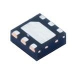
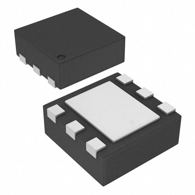
| 供应商器件封装 | 6-SON(2x2) |
| 其它名称 | 296-28951-1 |
| 包装 | 剪切带 (CT) |
| 安装类型 | 表面贴装 |
| 封装/外壳 | 6-WDFN 裸露焊盘 |
| 工作温度 | -40°C ~ 125°C |
| 标准包装 | 1 |
| 电压-跌落(典型值) | 0.28V @ 500mA |
| 电压-输入 | 2.7 V ~ 6.5 V |
| 电压-输出 | 2.85V |
| 电流-输出 | 500mA |
| 电流-限制(最小值) | 800mA |
| 稳压器拓扑 | 正,固定式 |
| 稳压器数 | 1 |


- 商务部:美国ITC正式对集成电路等产品启动337调查
- 曝三星4nm工艺存在良率问题 高通将骁龙8 Gen1或转产台积电
- 太阳诱电将投资9.5亿元在常州建新厂生产MLCC 预计2023年完工
- 英特尔发布欧洲新工厂建设计划 深化IDM 2.0 战略
- 台积电先进制程称霸业界 有大客户加持明年业绩稳了
- 达到5530亿美元!SIA预计今年全球半导体销售额将创下新高
- 英特尔拟将自动驾驶子公司Mobileye上市 估值或超500亿美元
- 三星加码芯片和SET,合并消费电子和移动部门,撤换高东真等 CEO
- 三星电子宣布重大人事变动 还合并消费电子和移动部门
- 海关总署:前11个月进口集成电路产品价值2.52万亿元 增长14.8%


PDF Datasheet 数据手册内容提取
Product Order Technical Tools & Support & Folder Now Documents Software Community TPS735 SBVS087M–JUNE2008–REVISEDJUNE2018 TPS735 500-mA, Low Quiescent Current, Low Noise, High PSRR, Low-Dropout Linear Regulator 1 Features 3 Description • InputVoltage:2.7Vto6.5V The TPS735 low-dropout (LDO), low-power linear 1 regulator offers excellent AC performance with very • 500-mALow-DropoutRegulatorWithEN low ground current. High power-supply rejection ratio • LowIQ:45μA (PSRR), low noise, fast start-up, and excellent line • MultipleOutputVoltageVersionsAvailable: and load transient responses are provided while consumingaverylow45-μA(typical)groundcurrent. – FixedOutputsof1.2Vto4.3V – AdjustableOutputsfrom1.25Vto6V The TPS735 device is stable with ceramic capacitors and uses an advanced BiCMOS fabrication process • HighPSRR:68dBat1kHz to yield a typical dropout voltage of 280 mV at 500- • LowNoise:13.2μVRMS mA output. The TPS735 device uses a precision • FastStart-UpTime:45 μs voltage reference and feedback loop to achieve overall accuracy of 2% (V > 2.2 V) over all load, • StableWithaCeramic,2.2-μF,Low-ESROutput OUT line, process, and temperature variations. This device Capacitor is fully specified from T = –40°C to +125°C and is J • ExcellentLoadandLineTransientResponse offered in a low-profile, 3 mm × 3 mm SON-8 • 2%OverallAccuracy(Load,Line,and packageanda2mm× 2mmWSON-6package. Temperature,V >2.2V) OUT DeviceInformation(1) • VeryLowDropout:280mVat500mA PARTNUMBER PACKAGE BODYSIZE(NOM) • 2-mm×2-mmWSON-6and WSON(6) 2.00mm×2.00mm 3-mm×3-mmSON-8Packages TPS735 SON(8) 3.00mm×3.00mm 2 Applications (1) For all available packages, see the orderable addendum at theendofthedatasheet. • PostDC-DCConverterRippleFiltering • IPNetworkCameras TypicalApplication • MacroBaseStations Optional input capacitor, C , to improve source IN • Thermostats impedance, noise, and PSRR VIN IN OUT VOUT TPS735 2.2 µF EN GND NR Ceramic V EN Optional bypass capacitor, C , to reduce output noise NR and increase PSRR 1 An IMPORTANT NOTICE at the end of this data sheet addresses availability, warranty, changes, use in safety-critical applications, intellectualpropertymattersandotherimportantdisclaimers.PRODUCTIONDATA.
TPS735 SBVS087M–JUNE2008–REVISEDJUNE2018 www.ti.com Table of Contents 1 Features.................................................................. 1 8 ApplicationandImplementation........................ 13 2 Applications........................................................... 1 8.1 ApplicationInformation............................................13 3 Description............................................................. 1 8.2 TypicalApplications................................................13 4 RevisionHistory..................................................... 2 9 PowerSupplyRecommendations...................... 16 5 PinConfigurationandFunctions......................... 4 10 Layout................................................................... 16 6 Specifications......................................................... 5 10.1 LayoutGuidelines.................................................16 6.1 AbsoluteMaximumRatings......................................5 10.2 LayoutExample....................................................16 6.2 ESDRatings..............................................................5 10.3 PowerDissipation.................................................17 6.3 RecommendedOperatingConditions.......................5 10.4 EstimatingJunctionTemperature.........................18 6.4 ThermalInformation..................................................6 10.5 PackageMounting................................................19 6.5 ElectricalCharacteristics...........................................7 11 DeviceandDocumentationSupport................. 20 6.6 TypicalCharacteristics..............................................8 11.1 DeviceSupport......................................................20 7 DetailedDescription............................................ 10 11.2 DocumentationSupport........................................20 7.1 Overview.................................................................10 11.3 Trademarks...........................................................20 7.2 FunctionalBlockDiagrams.....................................10 11.4 ElectrostaticDischargeCaution............................20 7.3 FeatureDescription.................................................11 11.5 Glossary................................................................20 7.4 DeviceFunctionalModes........................................12 12 Mechanical,Packaging,andOrderable Information........................................................... 20 4 Revision History NOTE:Pagenumbersforpreviousrevisionsmaydifferfrompagenumbersinthecurrentversion. ChangesfromRevisionL(January2015)toRevisionM Page • Updateddatasheettexttolatestdatasheetandtranslationstandards ............................................................................... 1 • Changed"Ultra-LowNoise"to"LowNoise"indocumenttitle ............................................................................................... 1 • ChangedLowI from46μAto45μAinFeatures,Description,andApplicationInformationsections................................. 1 Q • Changed"Standard"to"Ceramic"inFeatureslist................................................................................................................. 1 • Changed6-pinpackagefrom"SON"to"WSON"inFeatureslist ......................................................................................... 1 • Deletedprinters,WiFi®,WiMaxModules,cellularphones,smartphonesandmicroprocessorpowerfrom Applicationssection ............................................................................................................................................................... 1 • AddedpostDC/DCripplefiltering,IPnetworkcameras,macrobasestations,andthermostatstoApplicationssection.....1 • ChangedT toT inDescriptionsection ............................................................................................................................... 1 A J • Changed6-pinpackagefrom"SON"to"WSON"inDescriptionsection .............................................................................. 1 • ChangedpackageinDeviceInformationtablefromVSON(6)toWSON(6)........................................................................ 1 • Changed6-pinDRBpackagedesignatorfrom"VSON"to"SON"inPinConfigurationsandFunctionssection..................4 • Changed6-pinDRVpackagedesignatorfrom"VSON"to"WSON"inPinConfigurationsandFunctionssection ..............4 • Added"feedbackresistor"parametertoRecommendedOperatingConditionstable........................................................... 5 • ChangedDRVpackagedesignatorfrom"VSON"to"WSON"inThermalInformationtable ................................................ 6 • ChangedDRBpackagedesignatorfrom"VSON"to"SON"inThermalInformationtable ................................................... 6 • ChangedTPS735GroundPinCurrent(Disable)vsTemperatureinTypicalCharacteristicssection................................... 8 • ChangedTPS735DropoutVoltagevsOutputCurrentinTypicalCharacteristicssection..................................................... 8 • UpdatedEquation1 ............................................................................................................................................................. 14 • Changedx-axisscalefrom"10ms/div"to"10µs/div"inFigure17..................................................................................... 15 • Changedx-axisscalefrom"10ms/div"to"10µs/div"inFigure18..................................................................................... 15 • ChangedV startingvalueto0VinFigure19 ................................................................................................................ 15 OUT • UpdatedEquation2 ............................................................................................................................................................. 17 • UpdatedEquation3 ............................................................................................................................................................. 17 • ChangedDRVpackagedesignatorfrom"SON"to"WSON"inMeasuringPointsforT andT ......................................... 19 T B 2 SubmitDocumentationFeedback Copyright©2008–2018,TexasInstrumentsIncorporated ProductFolderLinks:TPS735
TPS735 www.ti.com SBVS087M–JUNE2008–REVISEDJUNE2018 Revision History (continued) • DeletedreferencestothermalinformationdocumentsinRelatedDocumentationsection ................................................ 20 ChangesfromRevisionK(August,2013)toRevisionL Page • AddedESDRatingstable,FeatureDescriptionsection,DeviceFunctionalModes,ApplicationandImplementation section,PowerSupplyRecommendationssection,Layoutsection,DeviceandDocumentationSupportsection,and Mechanical,Packaging,andOrderableInformationsections ............................................................................................... 1 • AddedfirstbulletiteminFeatureslist ................................................................................................................................... 1 • ChangedfourthbulletiteminFeatureslistto"fixedoutputsof1.2V" .................................................................................. 1 • ChangedeighthbulletiteminFeatureslist ........................................................................................................................... 1 • ChangedlastbulletinFeatureslist ....................................................................................................................................... 1 • ChangedlastApplicationslistitem........................................................................................................................................ 1 • ChangedPinConfigurationandFunctionssection;updatedtableformatandpindescriptionstomeetnewstandards .....4 • ChangedC valuenotationfrom0.01µFto10nFthroughoutElectricalCharacteristics.................................................... 7 NR • Changedfeedbackvoltageparametervaluesandmeasuredtestconditions....................................................................... 7 • Changedoutputcurrentlimitmaximumspecifiedvalue ........................................................................................................ 7 • Changedpower-supplyrejectionratiotypicalspecifiedvaluesfor100Hz,10kHz,and100kHzfrequencytest conditions............................................................................................................................................................................... 7 • Addednote(1)toFigure1 .................................................................................................................................................... 8 • Changedy-axistitleforFigure6............................................................................................................................................ 8 • Changedy-axistitleforFigure7............................................................................................................................................ 8 • ChangedfootnoteforFigure13............................................................................................................................................ 10 • Changedreferencetonoise-reductioncapacitor(C )tofeed-forwardcapacitor(C )inTransientResponse................. 11 NR FF • Changednoise-reductioncapacitortofeed-forwardcapacitorinFigure16........................................................................ 13 • Changedreferencesto"noise-reductioncapacitor"(C )to"feed-forwardcapacitor"(C )andsectiontitlefrom NR FF "FeedbackCapacitorRequirements"to"Feed-forwardCapacitorRequirements"inFeed-ForwardCapacitor Requirementssection........................................................................................................................................................... 14 • ChangedC valuenotationfrom0.01µFto10nFinOutputNoisesection...................................................................... 14 NR ChangesfromRevisionJ(May,2011)toRevisionK Page • AddedlastsentencetofirstparagraphofStartupandNoiseReductionCapacitorsection................................................ 11 ChangesfromRevisionI(April,2011)toRevisionJ Page • ReplacedtheDissipationRatingswithThermalInformation.................................................................................................. 6 • RevisedconditionsforTypicalCharacteristicstoincludestatementaboutTPS73525deviceavailability............................ 8 • AddedEstimatingJunctionTemperaturesection................................................................................................................. 18 • UpdatedPowerDissipationsection...................................................................................................................................... 19 ChangesfromRevisionH(November,2009)toRevisionI Page • CorrectedtypoinElectricalCharacteristicstableforV specification,DRVpackagetestconditions,V ≤2.2V...........7 OUT OUT ChangesfromRevisionG(March2009)toRevisionH Page • RevisedbulletpointinFeatureslisttoshowverylowdropoutof280mV............................................................................. 1 • Changeddropoutvoltagetypicalspecificationfrom250mVto280mV.................................................................................. 7 Copyright©2008–2018,TexasInstrumentsIncorporated SubmitDocumentationFeedback 3 ProductFolderLinks:TPS735
TPS735 SBVS087M–JUNE2008–REVISEDJUNE2018 www.ti.com 5 Pin Configuration and Functions DRBPackage DRVPackage 8-PinSONWithExposedThermalPad 6-PinWSONWithExposedThermalPad TopView TopView OUT 1 8 IN OUT 1 6 IN Thermal NC 2 7 NC FB,NR 2 Pad 5 NC Thermal Pad FB,NR 3 6 NC GND 3 4 EN GND 4 5 EN Not to scale NC-Nointernalconnection Not to scale PinFunctions PIN NO I/O DESCRIPTION NAME DRV DRB Inputsupply.A0.1-µFto1-µF,lowESRcapacitormustbeplacedfromthispintoground IN 6 8 I nearthedevice. GND 3 4 — Ground.ThepadmustbetiedtoGND. Drivingtheenablepin(EN)highturnsontheregulator.Drivingthispinlowputstheregulator EN 4 5 I intoshutdownmode.TheENpincanbeconnectedtotheINpinifnotused. Thispinisonlyavailableforthefixedvoltageversions.Connectinganexternalcapacitorto NR 2 3 — thispinbypassesnoisethatisgeneratedbytheinternalbandgapandallowstheoutput noisetobereducedtoverylowlevels.Themaximumrecommendedcapacitoris0.01μF. Thispinisonlyavailablefortheadjustableversion.TheFBpinistheinputtothecontrol-loop FB 2 3 I erroramplifier,andisusedtosettheoutputvoltageofthedevice.Thispinmustnotbeleft floating. Thispinistheoutputoftheregulator.Asmall,2.2-μFceramiccapacitorisrequiredfromthis OUT 1 1 O pintogroundtoassurestability.Theminimumoutputcapacitancerequiredforstabilityis2 µF. NC 5 2,6,7 — Notinternallyconnected. Thermalpad — 4 SubmitDocumentationFeedback Copyright©2008–2018,TexasInstrumentsIncorporated ProductFolderLinks:TPS735
TPS735 www.ti.com SBVS087M–JUNE2008–REVISEDJUNE2018 6 Specifications 6.1 Absolute Maximum Ratings at–40°C≤T andT ≤+125°C(unlessotherwisenoted).AllvoltagesarewithrespecttoGND.(1) J A MIN MAX UNIT V –0.3 7 V IN V –0.3 V +0.3 V EN IN Voltage V –0.3 1.6 V FB V –0.3 V +0.3 V OUT IN I Current Internallylimited A OUT P Continuoustotalpowerdissipation SeeThermalInformation D(tot) T Operatingjunctiontemperature –40 150 °C J T Storagetemperature –55 150 °C stg (1) StressesbeyondthoselistedasAbsoluteMaximumRatingsmaycausepermanentdamagetothedevice.Thesearestressratingsonly, andfunctionaloperationofthedeviceattheseoranyotherconditionsbeyondthoseindicatedasRecommendedOperatingConditions isnotimplied.Exposuretoabsolute-maximum-ratedconditionsforextendedperiodsmayaffectdevicereliability. 6.2 ESD Ratings VALUE UNIT Humanbodymodel(HBM),perANSI/ESDA/JEDECJS-001,allpins(1) ±2000 V V(ESD) Electrostaticdischarge Chargeddevicemodel(CDM),perJEDECspecificationJESD22-C101,all pins(2) ±500 V (1) JEDECdocumentJEP155statesthat500-VHBMallowssafemanufacturingwithastandardESDcontrolprocess. (2) JEDECdocumentJEP157statesthat250-VCDMallowssafemanufacturingwithastandardESDcontrolprocess. 6.3 Recommended Operating Conditions overoperatingjunctiontemperaturerange(unlessotherwisenoted) MIN NOM MAX UNIT V Inputvoltage 2.7 6.5 V IN V Outputvoltage V 6 V OUT FB I Outputcurrent(1) 0 500 mA OUT T Operatingfree-airtemperature –40 125 °C A C Inputcapacitor 1 µF IN C Outputcapacitor 2 µF OUT C Noisereductioncapacitor 10 nF NR C Feed-forwardcapacitor (2) 3 22 1000 pF FF R Feedbackresistor (2) 110 kΩ 2 (1) WhenoperatingatT near125°C,I is500μA. J OUT(min) (2) Adjustableversiononly. Copyright©2008–2018,TexasInstrumentsIncorporated SubmitDocumentationFeedback 5 ProductFolderLinks:TPS735
TPS735 SBVS087M–JUNE2008–REVISEDJUNE2018 www.ti.com 6.4 Thermal Information TPS735 (2) THERMALMETRIC(1) DRB(SON) DRV(WSON) UNIT 8PINS 6PINS R Junction-to-ambientthermalresistance (3) 52.2 65.1 °C/W θJA R Junction-to-case(top)thermalresistance (4) 59.4 85.6 °C/W θJC(top) R Junction-to-boardthermalresistance 19.3 34.7 °C/W θJB ψ Junction-to-topcharacterizationparameter (5) 2 1.6 °C/W JT ψ Junction-to-boardcharacterizationparameter (6) 19.3 35.1 °C/W JB R Junction-to-case(bottom)thermalresistance (7) 11.8 5.8 °C/W θJC(bot) (1) Formoreinformationabouttraditionalandnewthermalmetrics,seetheSemiconductorandICPackageThermalMetricsapplication report. (2) ThermaldatafortheDRB,DCQ,andDRVpackagesarederivedbythermalsimulationsbasedonJEDEC-standardmethodologyas specifiedintheJESD51series.Thefollowingassumptionsareusedinthesimulations: (a) i. DRB: The exposed pad is connected to the PCB ground layer through a 2 x 2 thermal via array. ii.DRV:TheexposedpadisconnectedtothePCBgroundlayerthrougha2x2thermalviaarray.Duetosizelimitationofthermal pad,0.8-mmpitcharrayisusedwhichisofftheJEDECstandard. (b) i.DRB:Thetopandbottomcopperlayersareassumedtohavea20%thermalconductivityofcopperrepresentinga20%copper coverage. ii DRV: The top and bottom copper layers are assumed to have a 20% thermal conductivity of copper representing a 20% copper coverage. (c)ThesedataweregeneratedwithonlyasingledeviceatthecenterofaJEDEChigh-K(2s2p)boardwith3-in×3-incopperarea.To understandtheeffectsofthecopperareaonthermalperformance,seethePowerDissipationandEstimatingJunctionTemperature sections. (3) Thejunction-to-ambientthermalresistanceundernaturalconvectionisobtainedinasimulationonaJEDEC-standard,high-Kboard,as specifiedinJESD51-7,inanenvironmentdescribedinJESD51-2a. (4) Thejunction-to-case(top)thermalresistanceisobtainedbysimulatingacoldplatetestonthetopofthepackage.NospecificJEDEC- standardtestexists,butaclosedescriptioncanbefoundintheANSISEMIstandardG30-88. (5) Thejunction-to-topcharacterizationparameter,ψ ,estimatesthejunctiontemperatureofadeviceinarealsystemandisextracted JT fromthesimulationdatatoobtainθ usingaproceduredescribedinJESD51-2a(sections6and7). JA (6) Thejunction-to-boardcharacterizationparameter,ψ ,estimatesthejunctiontemperatureofadeviceinarealsystemandisextracted JB fromthesimulationdatatoobtainθ usingaproceduredescribedinJESD51-2a(sections6and7). JA (7) Thejunction-to-case(bottom)thermalresistanceisobtainedbysimulatingacoldplatetestontheexposed(power)pad.Nospecific JEDECstandardtestexists,butaclosedescriptioncanbefoundintheANSISEMIstandardG30-88. 6 SubmitDocumentationFeedback Copyright©2008–2018,TexasInstrumentsIncorporated ProductFolderLinks:TPS735
TPS735 www.ti.com SBVS087M–JUNE2008–REVISEDJUNE2018 6.5 Electrical Characteristics overoperatingtemperaturerange(–40°C≤T ≤125°C),V =V +0.5Vor2.7V(whicheverisgreater),I =1mA, J IN OUT(nom) OUT V =V ,C =2.2μF,andC =10nF(unlessotherwisenoted).Fortheadjustableversion(TPS73501),V =3V. EN IN OUT NR OUT TypicalvaluesareatT =25°C. A PARAMETER TESTCONDITIONS MIN TYP MAX UNIT VIN Inputvoltage(1) 2.7 6.5 V Internalreference(adjustable VFB versiononly) TJ=25°C 1.196 1.208 1.220 V Outputvoltagerange VOUT (adjustableversiononly) VFB 6 V DCoutputaccuracy(1) 1mA≤IOUT≤500mA, VOUT>2.2V –2% ±1% 2% VOUT+0.5V≤VIN<6.5V VOUT≤2.2V –3% ±1% 3% ΔVOUT(ΔVIN) Lineregulation(1) VOUT(nom)+0.5V≤VIN≤6.5V 0.02 %/V ΔVOUT(ΔIOUT) Loadregulation 500µA≤IOUT≤500mA 0.005 %/mA Dropoutvoltage(2) VDO (VIN=VOUT(nom)–0.1V) IOUT=500mA 280 500 mV ILIM Outputcurrentlimit VVOINU≥T=2.07.9V×VOUT(nom),VIN=VOUT(nom)+0.9V 800 1170 1900 mA IGND Groundpincurrent 10mA≤IOUT≤500mA 45 65 μA ISHDN Shutdowncurrent VEN≤0V 0.15 1 μA Feedbackpincurrent IFB (adjustableversiononly) VOUT(nom)=1.2V –0.5 0.5 μA f=100Hz 66 PSRR Power-supplyrejectionratio VVIONU=T=3.28.585VV f=1kHz 68 dB CNR=0.01µF f=10kHz 44 IOUT=100mA f=100kHz 22 BW=10Hzto100kHz, CNR=10nF 11×VOUT Vn Outputnoisevoltage VOUT=2.8V CNR=none 95×VOUT μVRMS CNR=none 45 CNR=1nF 45 tSTR Start-uptime μs CNR=10nF 50 CNR=47nF 50 VEN(HI) Enablehigh(enabled) 1.2 V VEN(LO) Enablelow(shutdown) 0.4 V IEN(HI) Enablepincurrent,enabled VEN=VIN=6.5V 0.03 1 μA Shutdown,temperatureincreasing 165 Tsd Thermalshutdowntemperature °C Reset,temperaturedecreasing 145 UVLO Undervoltagelockout VINrising 1.9 2.2 2.65 V Vhys Hysteresis VINfalling 70 mV (1) MinimumV =V +V or2.7V,whicheverisgreater. IN OUT DO (2) V isnotmeasuredforthisfamilyofdeviceswithV <2.8VbecausetheminimumV =2.7V. DO OUT(nom) IN Copyright©2008–2018,TexasInstrumentsIncorporated SubmitDocumentationFeedback 7 ProductFolderLinks:TPS735
TPS735 SBVS087M–JUNE2008–REVISEDJUNE2018 www.ti.com 6.6 Typical Characteristics overoperatingtemperaturerange(T=–40°Cto+125°C),V =V +0.5Vor2.7V,whicheverisgreater;I =1mA, J IN OUT(nom) OUT V =V ,C =2.2μF,C =10nF.TypicalvaluesareatT =25°C,(unlessotherwisenoted). EN IN OUT NR J 0.5 0.5 T = 125°C J 0.4 0.4 T = 85°C Change in Output Voltage (%) ----0000000.......32101234 TTTTJJJ==== 20815°52C°°5CC°(1C) Change in Output Voltage (%) ----0000000.......32101234 TTTJJJJ=== –205°4C°0C°C J -0.5 TJ=–40°C -0.5 3 3.5 4 4.5 5 5.5 6 6.5 3 3.5 4 4.5 5 5.5 6 6.5 Input Voltage (V) Input Voltage (V) IOUT=100mA IOUT=100mA Figure1.TPS735LineRegulation Figure2.TPS735LineRegulation 2.86 2.55 T = 125°C T = 125°C 22..8854 TJJ= 85°C 2.54 TJJ= 85°C 2.83 TJ=–40°C 2.53 TJ= 25°C ge (V) 22..8821 ge (V) 22..5521 TTJJ== –0°4C0°C a a olt 2.8 olt 2.5 V V ut 2.79 ut 2.49 p p Out 2.78 Out 2.48 2.77 2.47 2.76 2.75 2.46 2.74 2.45 0 50 100 150 200 250 300 350 400 450 500 0 50 100 150 200 250 300 350 400 450 500 Load (mA) Load (mA) They-axisrangeis±2%of2.8V They-axisrangeis±2%of2.5V Figure3.TPS735LoadRegulation Figure4.TPS735LoadRegulation 60 500 V = 6.5 V 450 IN V = 5 V urrent on the GND Pin (A)m 54320000 TTTJJJ=== 281552°°5CC°C Ground Pin Current (nA) 433221105050500000000 VIINN= 3.3 V C 10 T = 0°C J 50 T =–40°C J 0 0 0 50 100 150 200 250 300 350 400 450 500 -40 -25 -10 5 20 35 50 65 80 95 110 125 Output Current (mA) JunctionTemperature (°C) Figure5.TPS735GroundPinCurrentvs Figure6.TPS735GroundPinCurrent(Disable)vs OutputCurrent Temperature 8 SubmitDocumentationFeedback Copyright©2008–2018,TexasInstrumentsIncorporated ProductFolderLinks:TPS735
TPS735 www.ti.com SBVS087M–JUNE2008–REVISEDJUNE2018 Typical Characteristics (continued) overoperatingtemperaturerange(T=–40°Cto+125°C),V =V +0.5Vor2.7V,whicheverisgreater;I =1mA, J IN OUT(nom) OUT V =V ,C =2.2μF,C =10nF.TypicalvaluesareatT =25°C,(unlessotherwisenoted). EN IN OUT NR J 400 90 T = +125°C 350 J 80 V) 300 TJ= +85°C 70 e (m 250 TJ= +25°C B) 60 oltag 200 R (d 50 Dropout V 115000 TJ=–4T0J°=C 0°C PSR 432000 IIIOOUUTT=== 1120 0m00A mmAA OUT 50 10 IOUT= 250 mA I = 500 mA 0 0 OUT 0 50 100 150 200 250 300 350 400 450 500 10 100 1k 10k 100k 1M 10M Output Current(mA) Frequency (Hz) V =0.4V (V –V =1V) EN IN OUT Figure7.TPS735DropoutVoltagevsOutputCurrent Figure8.Power-SupplyRippleRejectionvsFrequency 90 90 80 80 70 70 60 60 B) B) d 50 d 50 R ( R ( R 40 R 40 S S P I = 1 mA P 30 OUT 30 I = 1 mA I = 100 mA OUT OUT I = 100 mA 20 I = 200 mA 20 OUT OUT I = 200 mA I = 250 mA OUT 10 OUT 10 I = 250 mA I = 500 mA OUT OUT I = 500 mA 0 0 OUT 10 100 1k 10k 100k 1M 10M 10 100 1k 10k 100k 1M 10M Frequency (Hz) Frequency (Hz) (V –V =0.5V) (V –V =0.3V) IN OUT IN OUT Figure9.Power-SupplyRippleRejectionvsFrequency Figure10.Power-SupplyRippleRejectionvsFrequency 140 30 120 25 )S 100 )S RM RM 20 V V m 80 m se ( se ( 15 Noi 60 Noi Total 40 Total 10 20 5 0 0 0.01 0.1 1 10 0 5 10 15 20 25 Capacitance on the NR Pin (nF) Output Capacitance (mF) C =0.01µF,I =1mA NR OUT Figure11.TPS73525RMSNoisevsCNR Figure12.TPS735RMSNoisevsCOUT Copyright©2008–2018,TexasInstrumentsIncorporated SubmitDocumentationFeedback 9 ProductFolderLinks:TPS735
TPS735 SBVS087M–JUNE2008–REVISEDJUNE2018 www.ti.com 7 Detailed Description 7.1 Overview The TPS735 of low dropout (LDO) regulator combines the high performance required by radio frequency (RF) and precision analog applications with ultra-low current consumption. High PSRR is provided by a high-gain, high-bandwidth error loop with good supply rejection and very low headroom (V – V ). Fixed voltage versions IN OUT provideanoisereductionpintobypassnoisethatisgeneratedbytheband-gapreferenceandtoimprovePSRR. A quick-start circuit fast-charges this capacitor at start-up. The combination of high performance and low ground current make the TPS735 device designed for portable applications. All versions have thermal and overcurrent protectionandarespecifiedfrom –40°C ≤T ≤ +125°C. J 7.2 Functional Block Diagrams IN OUT 400W 2mA Current Limit EN Thermal Overshoot Shutdown Detect UVLO Quickstart 1.208 V (1) NR Bandgap 500 kW GND (1) The1.2-Vfixedvoltageversionhasa1-Vbandgapinsteadofa1.208-Vcircuit. Figure13. FixedVoltageVersions IN OUT 400W 3.3 MW Current Limit EN Thermal Overshoot Shutdown Detect UVLO 1.208 V FB Bandgap 500 kW GND Figure14. AdjustableVoltageVersions 10 SubmitDocumentationFeedback Copyright©2008–2018,TexasInstrumentsIncorporated ProductFolderLinks:TPS735
TPS735 www.ti.com SBVS087M–JUNE2008–REVISEDJUNE2018 7.3 Feature Description 7.3.1 InternalCurrentLimit The TPS735 internal current limit protects the regulator during fault conditions. During current limit, the output sourcesafixedamountofcurrentthatisindependentoftheoutputvoltage.Forreliableoperation,donotoperate thedeviceincurrentlimitforextendedperiodsoftime. The PMOS pass element in the TPS735 device contains a built-in body diode that conducts current when the voltage at the OUT pin exceeds the voltage at the IN pin. This current is not limited, so if extended reverse voltageoperationisexpected,externallimitingisappropriate. 7.3.2 Shutdown The enable pin (EN) is active high and is compatible with standard and low-voltage TTL-CMOS levels. When shutdowncapabilityisnotrequired,theENpincanconnecttotheINpin. 7.3.3 DropoutVoltage The TPS735 device uses a PMOS pass transistor to achieve low dropout. When (V – V ) is less than the IN OUT dropout voltage (V ), the PMOS pass device is in the linear region of operation and the input-to-output DO resistance (R ) of the PMOS pass element. V scales with the output current because the PMOS device (IN/OUT) DO operateslikearesistorindropout. Aswithanylinearregulator,PSRRandtransientresponsedegradesas(V –V )approachesdropout.Typical IN OUT Characteristicsshowsthiseffect;(seeFigure8throughFigure10). 7.3.4 Start-UpandNoiseReductionCapacitor Fixed voltage versions of the TPS735 use a quick-start circuit to charge the noise reduction (NR) capacitor (C ) NR if present (see Functional Block Diagrams). This architecture allows the combination of low output noise and fast start-up times. The NR pin is high impedance so a low-leakage C capacitor must be used. Most ceramic NR capacitors are appropriate in this configuration. A high-quality, COG-type (NPO) dielectric ceramic capacitor is recommendedforC whenusedinenvironmentswhereabruptchangesintemperaturecanoccur. NR For the fastest start-up, first apply V , then drive the enable (EN) pin high. If EN is tied to IN, start-up is slower. IN See Typical Applications . The quick-start switch closes for approximately 135 μs. To ensure that C is charged NR duringthequick-starttime,useacapacitorwithavalueofnomorethan0.01 μF. 7.3.5 TransientResponse As with any regulator, increasing the size of the output capacitor reduces overshoot and undershoot magnitude but increases the transient response duration. In the adjustable version, adding C between the OUT and FB FF pins improves stability and transient response performance. The transient response of the TPS735 device is enhanced by an active pulldown that engages when the output overshoots by approximately 5% or more when thedeviceisenabled.Thepull-downdeviceoperateslikea400-Ω resistortogroundwhenenabled. 7.3.6 UndervoltageLockout The TPS735 device uses an undervoltage lockout circuit to disable the output until the internal circuitry is operates properly. The UVLO circuit contains a deglitch feature so that the UVLO ignores undershoot transients ontheinputifthetransientsarelessthan50 μsinduration. 7.3.7 MinimumLoad The TPS735 device is stable with no output load. To meet the specified accuracy, a minimum load of 500 μA is required. If the output is below 500 µA and if the junction temperature is approximately 125°C, the output can increase enough to turn on the output pulldown. The output pulldown limits voltage drift to 5% (typically) but ground current can increase by approximately 50 μA. In most applications, the junction does not reach high temperatures at light loads because little power is dissipated. As a result, the specified ground current is valid at noloadinmostapplications. Copyright©2008–2018,TexasInstrumentsIncorporated SubmitDocumentationFeedback 11 ProductFolderLinks:TPS735
TPS735 SBVS087M–JUNE2008–REVISEDJUNE2018 www.ti.com Feature Description (continued) 7.3.8 ThermalProtection Thermal protection disables the output when the junction temperature increases to approximately 165°C, which allows the device to cool. When the junction temperature cools to approximately 145°C, the output circuitry is enabled. Depending on power dissipation, thermal resistance, and ambient temperature, the thermal protection circuit cycles on and off. This cycling limits the dissipation of the regulator and protects the regulator from damageasaresultofoverheating. Any tendency to activate the thermal protection circuit indicates excessive power dissipation or an inadequate heat sink. For reliable operation, limit junction temperature to 125°C (maximum). To estimate the thermal margin in a complete design (including heat sink), increase the ambient temperature until the thermal protection is triggered. Use worst-case loads and signal conditions. For reliable operation, trigger thermal protection at least 40°C above the maximum expected ambient condition of a particular application. This configuration produces a worst-casejunctiontemperatureof125°Catthehighestexpectedambienttemperatureandworst-caseload. The internal protection circuitry of the TPS735 protects against overload conditions. This protection circuitry is not intended to replace proper heat sinking. Continuously running the TPS735 into thermal shutdown degrades devicereliability. 7.4 Device Functional Modes 7.4.1 NormalOperation Thedeviceregulatestothenominaloutputvoltageunderthefollowingconditions: • The input voltage previously exceeded the UVLO voltage and did not decrease below the UVLO threshold minusV . hys • Theinputvoltageisgreaterthanthenominaloutputvoltagethatisaddedtothedropoutvoltage. • The enable voltage has previously exceeded the enable rising threshold voltage and has not decreased belowtheenablefallingthreshold. • Theoutputcurrentislessthanthecurrentlimit. • Thedevicejunctiontemperatureiswithinthespecifiedrange. 7.4.2 DropoutOperation If the input voltage is lower than the nominal output voltage plus the specified dropout voltage, but all other conditions are met for normal operation, the device operates in dropout mode. In this condition, the output voltage is equal to the input voltage minus the dropout voltage. The transient performance of the device degrades because the pass device is in a triode state and the LDO operates like a resistor. Line or load transientsindropoutcanresultinlargeoutputvoltagedeviations. 7.4.3 Disabled Thedeviceisdisabledunderthefollowingconditions: • TheinputvoltageislessthantheUVLOthresholdminusV ,orhasnotyetexceededtheUVLOthreshold. hys • The enable voltage is less than the enable falling threshold voltage or has not yet exceeded the enable rising threshold. • Thedevicejunctiontemperatureisgreaterthanthethermalshutdowntemperature. Table1liststheconditionsthatresultindifferentmodesofoperation. Table1.DeviceFunctionalModeComparison PARAMETER OPERATINGMODE V V I T IN EN OUT J Normalmode V >V +V andV >UVLO V >V I <I T <125°C IN OUTnom DO IN EN EN(HI) OUT LIM J Dropoutmode UVLO<V <V +V V >V — T <165°C IN OUTnom DO EN EN(HI) J Disabledmode (anytruecondition V <UVLO–V V <V — T >165°C IN hys EN EN(LO) J disablesthedevice) 12 SubmitDocumentationFeedback Copyright©2008–2018,TexasInstrumentsIncorporated ProductFolderLinks:TPS735
TPS735 www.ti.com SBVS087M–JUNE2008–REVISEDJUNE2018 8 Application and Implementation NOTE Information in the following applications sections is not part of the TI component specification, and TI does not warrant its accuracy or completeness. TI’s customers are responsible for determining suitability of components for their purposes. Customers should validateandtesttheirdesignimplementationtoconfirmsystemfunctionality. 8.1 Application Information The TPS735 LDO regulator provides a design with an ultra-low noise, high PSRR, low-dropout linear regulation withaverysmallgroundcurrent(5µA,typical). The devices are stable with ceramic capacitors and have a dropout voltage of 280 mV at the full output rating of 500 mA. The features of the TPS735 device enables the LDO regulators to be used in a wide variety of applicationswithminimaldesigncomplexity. 8.2 Typical Applications Figure 15 shows the basic circuit connections for fixed-voltage models. Figure 16 shows the connections for the adjustableoutputversion.R andR canbecalculatedforanyoutputvoltageusingtheformulainFigure16. 1 2 Optional input capacitor. May improve source impedance, noise, or PSRR. VIN IN OUT VOUT TPS735 2.2 µF EN GND NR Ceramic V EN Optional bypass capacitor to reduce output noise and increase PSRR. Figure15. TypicalApplicationCircuitforFixed-VoltageVersions Optional input capacitor. (R + R) May improve source V = 1 2 × 1.208 OUT R impedance, noise, or PSRR. 2 V IN OUT V IN OUT TPS735 R C 1 FF 2.2 µF EN GND FB Ceramic R 2 V EN Figure16. TypicalApplicationCircuitforAdjustable-VoltageVersions Copyright©2008–2018,TexasInstrumentsIncorporated SubmitDocumentationFeedback 13 ProductFolderLinks:TPS735
TPS735 SBVS087M–JUNE2008–REVISEDJUNE2018 www.ti.com Typical Applications (continued) 8.2.1 DesignRequirements 8.2.1.1 InputandOutputCapacitorRequirements Although an input capacitor is not required for stability, connecting a 0.1-μF to 1-μF low-equivalent series- resistance (ESR) capacitor across the input supply near the regulator is good analog design practice. This capacitorcounteractsreactiveinputsourcesandimprovestransientresponseandripplerejection.Ahigher-value capacitor may be required if large, fast, rise-time load transients are expected, or if the device is located several inches from the power source. If source impedance is not sufficiently low, a 0.1-μF input capacitor may be requiredtoensurestability. TheTPS735 device is designed to be stable with standard ceramic output capacitors of values 2 μF or larger. X5R- and X7R-type capacitors are best because these capacitors feature minimal variation in value and ESR over temperature. Maximum ESR of the output capacitor is < 1 Ω and, therefore, the output capacitortypemustbeceramicorconductivepolymerelectrolytic. 8.2.1.2 Feed-ForwardCapacitorRequirements The feed-forward capacitor (C ), shown in Figure 16, is required for stability. For a parallel combination of R FF 1 and R equal to 250 kΩ, any value between 3 pF to 1 nF can be used. Fixed-voltage versions have an internal 2 30-pF feed-forward capacitor that is quick-charged at start-up. Larger value capacitors improve noise slightly. TheTPS735deviceisstableinunity-gainconfigurations(theOUTpinistiedtotheFBpin)withoutC . FF 8.2.2 DetailedDesignProcedure 8.2.2.1 OutputNoise In most LDO regulators, the band gap is the dominant noise source. If a noise-reduction capacitor (C ) is used NR with the TPS735 device, the band gap does not contribute significantly to noise. Noise is dominated by the output resistor divider and the error-amplifier input. To minimize noise in a given application, use a 10-nF noise reduction capacitor. For the adjustable version, smaller value resistors in the output resistor divider reduce noise. A parallel combination that produces 2 μA of divider current has the same noise performance as a fixed voltage version with a C . To further optimize noise, set the ESR of the output capacitor to approximately 0.2 Ω. This NR configuration maximizes phase margin in the control loop, which reduces the total output noise up to 10%. TI recommendsamaximumcapacitorvalueof10nF. Equation 1 calculates the approximate integrated output noise from 10 Hz to 100 kHz with a C value of NR 10nF. V (mV )=11(mV /V)´V (V) n RMS RMS OUT (1) The TPS735adjustable version does not have the noise-reduction pin available, so ultra-low noise operation is notpossible.Noiseisminimizedaccordingtothepreviouslylistedrecommendations. 14 SubmitDocumentationFeedback Copyright©2008–2018,TexasInstrumentsIncorporated ProductFolderLinks:TPS735
TPS735 www.ti.com SBVS087M–JUNE2008–REVISEDJUNE2018 Typical Applications (continued) 8.2.3 ApplicationCurves atV =V +0.5Vor2.7V,whicheverisgreater;I =1mA,V =V ,C =2.2μF,C =10nF,and IN OUT(nom) OUT EN IN OUT NR T =25°C(unlessotherwisenoted) J 3.5 3.5 3 3 2.5 2.5 V) 2 V) 2 e ( e ( g 1.5 g 1.5 a a olt olt V 1 V 1 0.5 V ,C = 10mF 0.5 V ,C = 10mF OUT OUT OUT OUT 0 VOUT,COUT= 2.2mF 0 VOUT,COUT= 2.2mF V V EN EN -0.5 -0.5 10µs/div 10μs/div Figure17.TPS735TurnonResponse(V =V ) Figure18.TPS735TurnonResponseUsingEN IN EN 7 V COUT= 470mF OSCON OUT 200 mV/div 6 VIN= VEN COUT= 10mF 200 mV/div 5 e (V) 4 200 mV/div COUT= 2.2mF g 3 a olt V 2 1 VOUT 500 mA I 0 OUT 500 mA/div 1 mA -1 10 ms/div 10 ms/div RL=5Ω VIN=3V Figure19.TPS73525Power-UpandPower-Down Figure20.TPS735LoadTransientResponse (V =V ) IN EN COUT= 470mF OSCON 50 mV/div COUT= 10VmOFUT 50 mV/div 50 mV/div COUT= 2.2mF 4 V V OUT V IN 0.5 V/div 3 V 10 ms/div Figure21.TPS735LineTransientResponse Copyright©2008–2018,TexasInstrumentsIncorporated SubmitDocumentationFeedback 15 ProductFolderLinks:TPS735
TPS735 SBVS087M–JUNE2008–REVISEDJUNE2018 www.ti.com 9 Power Supply Recommendations Thedeviceisdesignedtooperatefromaninputvoltagesupplyrangebetween2.7Vand6.5V.Theinput voltagerangemustprovideadequateheadroomforthedevicetohavearegulatedoutput.Thisinputsupplymust bewell-regulated.Iftheinputsupplyisnoisy,additionalinputcapacitorswithlowESRcanhelpimproveoutput noise. 10 Layout 10.1 Layout Guidelines For best overall performance, place all circuit components on the same side of the circuit board and as near to the respective LDO pin connections as possible. Place ground return connections to the input and output capacitor, and to the LDO ground pin as close to each other as possible, connected by a wide, component-side, copper surface. The use of vias and long traces to create LDO component connections is strongly discouraged and negatively affects system performance. This grounding and layout scheme minimizes inductive parasitics, and as a result, reduces load-current transients, minimizes noise, and increases circuit stability. TI recommends using a ground reference plane, and is embedded in the printed circuit board (PCB) itself or located on the bottom side of the PCB opposite the components. This reference plane ensures accuracy of the output voltage, shieldstheLDOfromnoise,andoperatessimilartoathermalplanetospread(orsink)heatfromtheLDOdevice when connected to the exposed thermal pad. In most applications, this ground plane is required to meet thermal requirements. 10.1.1 BoardLayoutRecommendationstoImprovePSRRandNoisePerformance To improve AC performance (such as PSRR, output noise, and transient response), TI recommends designing the board with separate ground planes for V and V , with each ground plane connected only at the GND pin IN OUT ofthedevice.Inaddition,thegroundconnectionforthebypasscapacitormustconnectdirectlytotheGNDpinof thedevice. 10.2 Layout Example Input GND Plane V OUT CIN(1) OUT 1 8 IN V NC 2 7 NC IN COUT(1) CNR(1) ThPearmdal NR/FB 3 6 NC GND 4 5 EN Output GND Plane (1) C andC are0603capacitorsandC isa0402capacitor.Thefootprintisshowntoscalewithpackagesize. IN OUT NR Figure22. TPS735FixedVersionLayoutReferenceDiagram 16 SubmitDocumentationFeedback Copyright©2008–2018,TexasInstrumentsIncorporated ProductFolderLinks:TPS735
TPS735 www.ti.com SBVS087M–JUNE2008–REVISEDJUNE2018 10.3 Power Dissipation Theabilitytoremoveheatfromthedieisdifferentforeachpackagetype,whichpresentsdifferentconsiderations in the PCB layout. The PCB area around the device that is free of other components moves the heat from the device to the ambient air. Performance data for JEDEC low- and high-K boards are shown in the Thermal Information section. Heavier copper increases the effectiveness in removing heat from the device. The addition ofplatedthrough-holestoheat-dissipatinglayersimprovestheheatsinkeffectiveness. Power dissipation depends on input voltage and load conditions. Power dissipation can be approximated by the productoftheoutputcurrentandthevoltagedropacrosstheoutputpasselement,asEquation2 shows. P =(V - V )´I D IN OUT OUT (2) NOTE When the device is used in a condition of high input and low output voltages, P can D exceed the junction temperature rating even when the ambient temperature is at room temperature. Equation3isanexamplecalculationforthepowerdissipation(P )oftheDRBpackage. D P =(6.5V -1.2V)´500mA =2.65W D (3) Power dissipation can be minimized and greater efficiency can be achieved by using the lowest possible input voltagenecessarytoachievetherequiredoutputperformance. On the DRB package, the primary conduction path for heat is through the exposed thermal pad to the PCB. The pad can be connected to ground or left floating. The pad must be attached to an appropriate amount of copper PCB area to ensure that the device does not overheat. The maximum allowable junction-to-ambient thermal resistance depends on the maximum ambient temperature, maximum device junction temperature, and power dissipationofthedevice.Equation4calculatesthemaximumjunction-to-ambientthermalresistance. (cid:11)125qC(cid:16)T (cid:12) R A TJA P D (4) Copyright©2008–2018,TexasInstrumentsIncorporated SubmitDocumentationFeedback 17 ProductFolderLinks:TPS735
TPS735 SBVS087M–JUNE2008–REVISEDJUNE2018 www.ti.com Power Dissipation (continued) Figure23estimatesthemaximumR andtheminimumamountofPCBcopperarearequiredtoheatsink. θJA 160 DRV 140 DRB 120 W) 100 °(C/ 80 A qJ 60 40 20 0 0 1 2 3 4 5 6 7 8 9 10 Board Copper Area (in2) Note: θ valueatboardsizeof9in2(thatis,3in×3in)isaJEDECstandard. JA Figure23. θ vsBoardSize JA Figure23showsthevariationof θ asafunctionofgroundplanecopperareaintheboard.Itisintendedonlyas JA a guideline to demonstrate the effects of heat spreading in the ground plane and must not be used to estimate actualthermalperformanceinrealapplicationenvironments. NOTE When the device is mounted on an application PCB, it is strongly recommended to use Ψ and Ψ ,asexplainedintheEstimatingJunctionTemperature section. JT JB 10.4 Estimating Junction Temperature Using the thermal metrics Ψ and Ψ , as the table shows, the junction temperature can be estimated with JT JB correspondingformulas(Equation5),whicharemoreaccuratethanthevalueofT throughcalculationwithθ . J JA Y : T = T +Y ·P JT J T JT D Y : T = T +Y ·P JB J B JB D where: • P isthepowerdissipationcalculatedwithEquation2, D • T isthetemperatureatthecenter-topofthedevicepackage,and T • T isthePCBtemperaturemeasured1mmawayfromthedevicepackageonthePCBsurface(asshownin B Figure25). (5) NOTE Both T and T can be measured on actual application boards using a thermo-gun (an T B infraredthermometer). For more information about measuring T and T , see Using New Thermal Metrics, available for download at T B www.ti.com. 18 SubmitDocumentationFeedback Copyright©2008–2018,TexasInstrumentsIncorporated ProductFolderLinks:TPS735
TPS735 www.ti.com SBVS087M–JUNE2008–REVISEDJUNE2018 Estimating Junction Temperature (continued) According to Figure 24, the new thermal metrics (Ψ and Ψ ) do not depend on the copper area. Using Ψ or JT JB JT Ψ withEquation5 canestimateT bymeasuringT orT onanapplicationboard. JB J T B 35 30 W) 25 DRV Y C/ DRB JB °( 20 B YJ d 15 n a T YJ 10 DRV Y 5 DRB JT 0 0 1 2 3 4 5 6 7 8 9 10 Board Copper Area (in2) Figure24. Ψ andΨ vsBoardSize JT JB T on top ofT device TofT doenv tiocpe T on PCB T on PCB suBrface suBrface 1 mm 1 mm See note (1) (a) Example DRB (SON) Package Measurement (b) Example DRV (WSON) Package Measurement (1) Powerdissipationmaylimitoperatingrange.SeeThermalInformation. Figure25. MeasuringPointsforT andT T B 10.5 Package Mounting SolderpadfootprintrecommendationsfortheTPS735deviceisavailablefromtheTIwebsiteatwww.ti.com. Copyright©2008–2018,TexasInstrumentsIncorporated SubmitDocumentationFeedback 19 ProductFolderLinks:TPS735
TPS735 SBVS087M–JUNE2008–REVISEDJUNE2018 www.ti.com 11 Device and Documentation Support 11.1 Device Support 11.1.1 DevelopmentSupport 11.1.1.1 EvaluationModules Two evaluation modules (EVMs) are available to assist in the initial circuit performance evaluation using the TPS735. The TPS73501EVM-276 evaluation module and the TPS73525EVM-276 Evaluation Module (and related user guide) can be requested at the TI website through the product folders or purchased directly from the TIeStore. 11.1.2 DeviceNomenclature Table2.DeviceNomenclature(1) PRODUCT V OUT xx(x)isthenominaloutputvoltage.Foroutputvoltageswitharesolutionof100mV,two digitsareusedintheorderingnumber;otherwise,threedigitsareused(forexample,33= 3.3V;125=1.25V). TPS735xx(x)yyyz yyyisthepackagedesignator. zisthetapeandreelquantity(R=3000,T=250). 01istheadjustableversion. (1) ForthemostcurrentpackageandorderinginformationseethePackageOptionAddendumattheendofthisdocument,orseetheTI websiteatwww.ti.com. 11.2 Documentation Support 11.2.1 RelatedDocumentation Forrelateddocumentation,seethefollowing: • TexasInstruments,TPS735EVM-276UserGuide 11.3 Trademarks Alltrademarksarethepropertyoftheirrespectiveowners. 11.4 Electrostatic Discharge Caution This integrated circuit can be damaged by ESD. Texas Instruments recommends that all integrated circuits be handled with appropriateprecautions.Failuretoobserveproperhandlingandinstallationprocedurescancausedamage. ESDdamagecanrangefromsubtleperformancedegradationtocompletedevicefailure.Precisionintegratedcircuitsmaybemore susceptibletodamagebecauseverysmallparametricchangescouldcausethedevicenottomeetitspublishedspecifications. 11.5 Glossary SLYZ022—TIGlossary. Thisglossarylistsandexplainsterms,acronyms,anddefinitions. 12 Mechanical, Packaging, and Orderable Information The following pages include mechanical, packaging, and orderable information. This information is the most current data available for the designated devices. This data is subject to change without notice and revision of thisdocument.Forbrowser-basedversionsofthisdatasheet,refertotheleft-handnavigation. 20 SubmitDocumentationFeedback Copyright©2008–2018,TexasInstrumentsIncorporated ProductFolderLinks:TPS735
PACKAGE OPTION ADDENDUM www.ti.com 6-Feb-2020 PACKAGING INFORMATION Orderable Device Status Package Type Package Pins Package Eco Plan Lead/Ball Finish MSL Peak Temp Op Temp (°C) Device Marking Samples (1) Drawing Qty (2) (6) (3) (4/5) TPS73501DRBR ACTIVE SON DRB 8 3000 Green (RoHS NIPDAU Level-2-260C-1 YEAR -40 to 125 CBK & no Sb/Br) TPS73501DRBT ACTIVE SON DRB 8 250 Green (RoHS NIPDAU Level-2-260C-1 YEAR -40 to 125 CBK & no Sb/Br) TPS73501DRVR ACTIVE WSON DRV 6 3000 Green (RoHS NIPDAU Level-1-260C-UNLIM -40 to 125 SDR & no Sb/Br) TPS73501DRVT ACTIVE WSON DRV 6 250 Green (RoHS NIPDAU Level-1-260C-UNLIM -40 to 125 SDR & no Sb/Br) TPS73512DRBR ACTIVE SON DRB 8 3000 Green (RoHS NIPDAU Level-2-260C-1 YEAR -40 to 125 QTT & no Sb/Br) TPS73512DRBT ACTIVE SON DRB 8 250 Green (RoHS NIPDAU Level-2-260C-1 YEAR -40 to 125 QTT & no Sb/Br) TPS73515DRBR ACTIVE SON DRB 8 3000 Green (RoHS NIPDAU Level-2-260C-1 YEAR -40 to 125 QWH & no Sb/Br) TPS73515DRBT ACTIVE SON DRB 8 250 Green (RoHS NIPDAU Level-2-260C-1 YEAR -40 to 125 QWH & no Sb/Br) TPS73525DRBR ACTIVE SON DRB 8 3000 Green (RoHS NIPDAU Level-2-260C-1 YEAR -40 to 125 CBM & no Sb/Br) TPS73525DRBRG4 ACTIVE SON DRB 8 3000 Green (RoHS NIPDAU Level-2-260C-1 YEAR -40 to 125 CBM & no Sb/Br) TPS73525DRBT ACTIVE SON DRB 8 250 Green (RoHS NIPDAU Level-2-260C-1 YEAR -40 to 125 CBM & no Sb/Br) TPS73525DRVR ACTIVE WSON DRV 6 3000 Green (RoHS NIPDAU Level-1-260C-UNLIM -40 to 125 NSW & no Sb/Br) TPS73525DRVT ACTIVE WSON DRV 6 250 Green (RoHS NIPDAU Level-1-260C-UNLIM -40 to 125 NSW & no Sb/Br) TPS73527DRVR ACTIVE WSON DRV 6 3000 Green (RoHS NIPDAU Level-1-260C-UNLIM -40 to 125 RAK & no Sb/Br) TPS73527DRVT ACTIVE WSON DRV 6 250 Green (RoHS NIPDAU Level-1-260C-UNLIM -40 to 125 RAK & no Sb/Br) TPS735285DRVR ACTIVE WSON DRV 6 3000 Green (RoHS NIPDAU Level-1-260C-UNLIM -40 to 125 RAW & no Sb/Br) TPS735285DRVT ACTIVE WSON DRV 6 250 Green (RoHS NIPDAU Level-1-260C-UNLIM -40 to 125 RAW & no Sb/Br) Addendum-Page 1
PACKAGE OPTION ADDENDUM www.ti.com 6-Feb-2020 Orderable Device Status Package Type Package Pins Package Eco Plan Lead/Ball Finish MSL Peak Temp Op Temp (°C) Device Marking Samples (1) Drawing Qty (2) (6) (3) (4/5) TPS73533DRBR ACTIVE SON DRB 8 3000 Green (RoHS NIPDAU Level-2-260C-1 YEAR -40 to 125 CVY & no Sb/Br) TPS73533DRBT ACTIVE SON DRB 8 250 Green (RoHS NIPDAU Level-2-260C-1 YEAR -40 to 125 CVY & no Sb/Br) TPS73533DRVR ACTIVE WSON DRV 6 3000 Green (RoHS NIPDAU | NIPDAUAG Level-1-260C-UNLIM -40 to 125 CVY & no Sb/Br) TPS73533DRVT ACTIVE WSON DRV 6 250 Green (RoHS NIPDAU | NIPDAUAG Level-1-260C-UNLIM -40 to 125 CVY & no Sb/Br) TPS73534DRBR ACTIVE SON DRB 8 3000 Green (RoHS NIPDAU Level-2-260C-1 YEAR -40 to 125 QTU & no Sb/Br) TPS73534DRBT ACTIVE SON DRB 8 250 Green (RoHS NIPDAU Level-2-260C-1 YEAR -40 to 125 QTU & no Sb/Br) (1) The marketing status values are defined as follows: ACTIVE: Product device recommended for new designs. LIFEBUY: TI has announced that the device will be discontinued, and a lifetime-buy period is in effect. NRND: Not recommended for new designs. Device is in production to support existing customers, but TI does not recommend using this part in a new design. PREVIEW: Device has been announced but is not in production. Samples may or may not be available. OBSOLETE: TI has discontinued the production of the device. (2) RoHS: TI defines "RoHS" to mean semiconductor products that are compliant with the current EU RoHS requirements for all 10 RoHS substances, including the requirement that RoHS substance do not exceed 0.1% by weight in homogeneous materials. Where designed to be soldered at high temperatures, "RoHS" products are suitable for use in specified lead-free processes. TI may reference these types of products as "Pb-Free". RoHS Exempt: TI defines "RoHS Exempt" to mean products that contain lead but are compliant with EU RoHS pursuant to a specific EU RoHS exemption. Green: TI defines "Green" to mean the content of Chlorine (Cl) and Bromine (Br) based flame retardants meet JS709B low halogen requirements of <=1000ppm threshold. Antimony trioxide based flame retardants must also meet the <=1000ppm threshold requirement. (3) MSL, Peak Temp. - The Moisture Sensitivity Level rating according to the JEDEC industry standard classifications, and peak solder temperature. (4) There may be additional marking, which relates to the logo, the lot trace code information, or the environmental category on the device. (5) Multiple Device Markings will be inside parentheses. Only one Device Marking contained in parentheses and separated by a "~" will appear on a device. If a line is indented then it is a continuation of the previous line and the two combined represent the entire Device Marking for that device. (6) Lead/Ball Finish - Orderable Devices may have multiple material finish options. Finish options are separated by a vertical ruled line. Lead/Ball Finish values may wrap to two lines if the finish value exceeds the maximum column width. Addendum-Page 2
PACKAGE OPTION ADDENDUM www.ti.com 6-Feb-2020 Important Information and Disclaimer:The information provided on this page represents TI's knowledge and belief as of the date that it is provided. TI bases its knowledge and belief on information provided by third parties, and makes no representation or warranty as to the accuracy of such information. Efforts are underway to better integrate information from third parties. TI has taken and continues to take reasonable steps to provide representative and accurate information but may not have conducted destructive testing or chemical analysis on incoming materials and chemicals. TI and TI suppliers consider certain information to be proprietary, and thus CAS numbers and other limited information may not be available for release. In no event shall TI's liability arising out of such information exceed the total purchase price of the TI part(s) at issue in this document sold by TI to Customer on an annual basis. OTHER QUALIFIED VERSIONS OF TPS735 : •Automotive: TPS735-Q1 NOTE: Qualified Version Definitions: •Automotive - Q100 devices qualified for high-reliability automotive applications targeting zero defects Addendum-Page 3
PACKAGE MATERIALS INFORMATION www.ti.com 17-May-2020 TAPE AND REEL INFORMATION *Alldimensionsarenominal Device Package Package Pins SPQ Reel Reel A0 B0 K0 P1 W Pin1 Type Drawing Diameter Width (mm) (mm) (mm) (mm) (mm) Quadrant (mm) W1(mm) TPS73501DRBR SON DRB 8 3000 330.0 12.4 3.3 3.3 1.1 8.0 12.0 Q2 TPS73501DRBT SON DRB 8 250 180.0 12.5 3.3 3.3 1.1 8.0 12.0 Q2 TPS73501DRVR WSON DRV 6 3000 178.0 8.4 2.25 2.25 1.0 4.0 8.0 Q2 TPS73501DRVT WSON DRV 6 250 178.0 8.4 2.25 2.25 1.0 4.0 8.0 Q2 TPS73501DRVT WSON DRV 6 250 179.0 8.4 2.2 2.2 1.2 4.0 8.0 Q2 TPS73512DRBR SON DRB 8 3000 330.0 12.4 3.3 3.3 1.1 8.0 12.0 Q2 TPS73512DRBT SON DRB 8 250 180.0 12.4 3.3 3.3 1.1 8.0 12.0 Q2 TPS73515DRBR SON DRB 8 3000 330.0 12.4 3.3 3.3 1.1 8.0 12.0 Q2 TPS73515DRBT SON DRB 8 250 180.0 12.5 3.3 3.3 1.1 8.0 12.0 Q2 TPS73525DRBR SON DRB 8 3000 330.0 12.4 3.3 3.3 1.1 8.0 12.0 Q2 TPS73525DRBT SON DRB 8 250 180.0 12.5 3.3 3.3 1.1 8.0 12.0 Q2 TPS73525DRVR WSON DRV 6 3000 179.0 8.4 2.2 2.2 1.2 4.0 8.0 Q2 TPS73525DRVT WSON DRV 6 250 179.0 8.4 2.2 2.2 1.2 4.0 8.0 Q2 TPS73527DRVR WSON DRV 6 3000 179.0 8.4 2.2 2.2 1.2 4.0 8.0 Q2 TPS73527DRVR WSON DRV 6 3000 178.0 8.4 2.25 2.25 1.0 4.0 8.0 Q2 TPS73527DRVT WSON DRV 6 250 179.0 8.4 2.2 2.2 1.2 4.0 8.0 Q2 TPS735285DRVR WSON DRV 6 3000 179.0 8.4 2.2 2.2 1.2 4.0 8.0 Q2 TPS735285DRVT WSON DRV 6 250 179.0 8.4 2.2 2.2 1.2 4.0 8.0 Q2 PackMaterials-Page1
PACKAGE MATERIALS INFORMATION www.ti.com 17-May-2020 Device Package Package Pins SPQ Reel Reel A0 B0 K0 P1 W Pin1 Type Drawing Diameter Width (mm) (mm) (mm) (mm) (mm) Quadrant (mm) W1(mm) TPS73533DRBR SON DRB 8 3000 330.0 12.4 3.3 3.3 1.1 8.0 12.0 Q2 TPS73533DRBR SON DRB 8 3000 330.0 12.4 3.3 3.3 1.1 8.0 12.0 Q2 TPS73533DRBT SON DRB 8 250 180.0 12.5 3.3 3.3 1.1 8.0 12.0 Q2 TPS73533DRVR WSON DRV 6 3000 178.0 8.4 2.25 2.25 1.0 4.0 8.0 Q2 TPS73533DRVR WSON DRV 6 3000 179.0 8.4 2.2 2.2 1.2 4.0 8.0 Q2 TPS73533DRVT WSON DRV 6 250 178.0 8.4 2.25 2.25 1.0 4.0 8.0 Q2 TPS73533DRVT WSON DRV 6 250 179.0 8.4 2.2 2.2 1.2 4.0 8.0 Q2 TPS73534DRBR SON DRB 8 3000 330.0 12.4 3.3 3.3 1.1 8.0 12.0 Q2 TPS73534DRBT SON DRB 8 250 180.0 12.4 3.3 3.3 1.1 8.0 12.0 Q2 *Alldimensionsarenominal Device PackageType PackageDrawing Pins SPQ Length(mm) Width(mm) Height(mm) TPS73501DRBR SON DRB 8 3000 338.0 355.0 50.0 TPS73501DRBT SON DRB 8 250 338.0 355.0 50.0 TPS73501DRVR WSON DRV 6 3000 205.0 200.0 33.0 TPS73501DRVT WSON DRV 6 250 205.0 200.0 33.0 TPS73501DRVT WSON DRV 6 250 203.0 203.0 35.0 TPS73512DRBR SON DRB 8 3000 367.0 367.0 35.0 TPS73512DRBT SON DRB 8 250 210.0 185.0 35.0 TPS73515DRBR SON DRB 8 3000 338.0 355.0 50.0 PackMaterials-Page2
PACKAGE MATERIALS INFORMATION www.ti.com 17-May-2020 Device PackageType PackageDrawing Pins SPQ Length(mm) Width(mm) Height(mm) TPS73515DRBT SON DRB 8 250 338.0 355.0 50.0 TPS73525DRBR SON DRB 8 3000 338.0 355.0 50.0 TPS73525DRBT SON DRB 8 250 338.0 355.0 50.0 TPS73525DRVR WSON DRV 6 3000 203.0 203.0 35.0 TPS73525DRVT WSON DRV 6 250 203.0 203.0 35.0 TPS73527DRVR WSON DRV 6 3000 203.0 203.0 35.0 TPS73527DRVR WSON DRV 6 3000 205.0 200.0 33.0 TPS73527DRVT WSON DRV 6 250 203.0 203.0 35.0 TPS735285DRVR WSON DRV 6 3000 203.0 203.0 35.0 TPS735285DRVT WSON DRV 6 250 203.0 203.0 35.0 TPS73533DRBR SON DRB 8 3000 338.0 355.0 50.0 TPS73533DRBR SON DRB 8 3000 367.0 367.0 35.0 TPS73533DRBT SON DRB 8 250 338.0 355.0 50.0 TPS73533DRVR WSON DRV 6 3000 205.0 200.0 33.0 TPS73533DRVR WSON DRV 6 3000 203.0 203.0 35.0 TPS73533DRVT WSON DRV 6 250 205.0 200.0 33.0 TPS73533DRVT WSON DRV 6 250 203.0 203.0 35.0 TPS73534DRBR SON DRB 8 3000 367.0 367.0 35.0 TPS73534DRBT SON DRB 8 250 210.0 185.0 35.0 PackMaterials-Page3
GENERIC PACKAGE VIEW DRV 6 WSON - 0.8 mm max height PLASTIC SMALL OUTLINE - NO LEAD Images above are just a representation of the package family, actual package may vary. Refer to the product data sheet for package details. 4206925/F
PACKAGE OUTLINE DRV0006A WSON - 0.8 mm max height SCALE 5.500 PLASTIC SMALL OUTLINE - NO LEAD B 2.1 A 1.9 PIN 1 INDEX AREA 2.1 1.9 0.8 C 0.7 SEATING PLANE 0.08 C (0.2) TYP 1 0.1 0.05 EXPOSED 0.00 THERMAL PAD 3 4 2X 7 1.3 1.6 0.1 6 1 4X 0.65 0.35 6X PIN 1 ID 0.3 0.25 6X (OPTIONAL) 0.2 0.1 C A B 0.05 C 4222173/B 04/2018 NOTES: 1. All linear dimensions are in millimeters. Any dimensions in parenthesis are for reference only. Dimensioning and tolerancing per ASME Y14.5M. 2. This drawing is subject to change without notice. 3. The package thermal pad must be soldered to the printed circuit board for thermal and mechanical performance. www.ti.com
EXAMPLE BOARD LAYOUT DRV0006A WSON - 0.8 mm max height PLASTIC SMALL OUTLINE - NO LEAD 6X (0.45) (1) 1 7 6X (0.3) 6 SYMM (1.6) (1.1) 4X (0.65) 4 3 (R0.05) TYP SYMM ( 0.2) VIA (1.95) TYP LAND PATTERN EXAMPLE SCALE:25X 0.07 MAX 0.07 MIN ALL AROUND ALL AROUND SOLDER MASK METAL METAL UNDER SOLDER MASK OPENING SOLDER MASK OPENING NON SOLDER MASK DEFINED SOLDER MASK (PREFERRED) DEFINED SOLDER MASK DETAILS 4222173/B 04/2018 NOTES: (continued) 4. This package is designed to be soldered to a thermal pad on the board. For more information, see Texas Instruments literature number SLUA271 (www.ti.com/lit/slua271). 5. Vias are optional depending on application, refer to device data sheet. If some or all are implemented, recommended via locations are shown. www.ti.com
EXAMPLE STENCIL DESIGN DRV0006A WSON - 0.8 mm max height PLASTIC SMALL OUTLINE - NO LEAD SYMM 6X (0.45) METAL 1 7 6X (0.3) 6 (0.45) SYMM 4X (0.65) (0.7) 4 3 (R0.05) TYP (1) (1.95) SOLDER PASTE EXAMPLE BASED ON 0.125 mm THICK STENCIL EXPOSED PAD #7 88% PRINTED SOLDER COVERAGE BY AREA UNDER PACKAGE SCALE:30X 4222173/B 04/2018 NOTES: (continued) 6. Laser cutting apertures with trapezoidal walls and rounded corners may offer better paste release. IPC-7525 may have alternate design recommendations. www.ti.com
PACKAGE OUTLINE DRV0006D WSON - 0.8 mm max height SCALE 5.500 PLASTIC SMALL OUTLINE - NO LEAD B 2.1 A 1.9 PIN 1 INDEX AREA 2.1 1.9 0.8 C 0.7 SEATING PLANE 0.08 C (0.2) TYP 1 0.1 0.05 EXPOSED 0.00 THERMAL PAD 3 4 2X 7 1.3 1.6 0.1 6 1 4X 0.65 0.35 6X PIN 1 ID 0.3 0.25 6X (OPTIONAL) 0.2 0.1 C A B 0.05 C 4225563/A 12/2019 NOTES: 1. All linear dimensions are in millimeters. Any dimensions in parenthesis are for reference only. Dimensioning and tolerancing per ASME Y14.5M. 2. This drawing is subject to change without notice. 3. The package thermal pad must be soldered to the printed circuit board for thermal and mechanical performance. www.ti.com
EXAMPLE BOARD LAYOUT DRV0006D WSON - 0.8 mm max height PLASTIC SMALL OUTLINE - NO LEAD 6X (0.45) (1) 1 7 6X (0.3) 6 SYMM (1.6) (1.1) 4X (0.65) 4 3 (R0.05) TYP SYMM ( 0.2) VIA (1.95) TYP LAND PATTERN EXAMPLE EXPOSED METAL SHOWN SCALE:25X 0.07 MAX 0.07 MIN ALL AROUND ALL AROUND EXPOSED EXPOSED METAL METAL SOLDER MASK METAL METAL UNDER SOLDER MASK OPENING SOLDER MASK OPENING NON SOLDER MASK DEFINED SOLDER MASK (PREFERRED) DEFINED SOLDER MASK DETAILS 4225563/A 12/2019 NOTES: (continued) 4. This package is designed to be soldered to a thermal pad on the board. For more information, see Texas Instruments literature number SLUA271 (www.ti.com/lit/slua271). 5. Vias are optional depending on application, refer to device data sheet. If some or all are implemented, recommended via locations are shown. www.ti.com
EXAMPLE STENCIL DESIGN DRV0006D WSON - 0.8 mm max height PLASTIC SMALL OUTLINE - NO LEAD SYMM 6X (0.45) METAL 1 7 6X (0.3) 6 (0.45) SYMM 4X (0.65) (0.7) 4 3 (R0.05) TYP (1) (1.95) SOLDER PASTE EXAMPLE BASED ON 0.125 mm THICK STENCIL EXPOSED PAD #7 88% PRINTED SOLDER COVERAGE BY AREA UNDER PACKAGE SCALE:30X 4225563/A 12/2019 NOTES: (continued) 6. Laser cutting apertures with trapezoidal walls and rounded corners may offer better paste release. IPC-7525 may have alternate design recommendations. www.ti.com
None
PACKAGE OUTLINE DRB0008A VSON - 1 mm max height SCALE 4.000 PLASTIC SMALL OUTLINE - NO LEAD 3.1 B A 2.9 PIN 1 INDEX AREA 3.1 2.9 C 1 MAX SEATING PLANE 0.05 0.08 C DIM A 0.00 OPT 1 OPT 2 1.5 0.1 (0.1) (0.2) 4X (0.23) EXPOSED (DIM A) TYP THERMAL PAD 4 5 2X 1.95 1.75 0.1 8 1 6X 0.65 0.37 8X 0.25 PIN 1 ID 0.1 C A B (OPTIONAL) (0.65) 0.05 C 0.5 8X 0.3 4218875/A 01/2018 NOTES: 1. All linear dimensions are in millimeters. Any dimensions in parenthesis are for reference only. Dimensioning and tolerancing per ASME Y14.5M. 2. This drawing is subject to change without notice. 3. The package thermal pad must be soldered to the printed circuit board for thermal and mechanical performance. www.ti.com
EXAMPLE BOARD LAYOUT DRB0008A VSON - 1 mm max height PLASTIC SMALL OUTLINE - NO LEAD (1.5) (0.65) SYMM 8X (0.6) (0.825) 8X (0.31) 1 8 SYMM (1.75) (0.625) 6X (0.65) 4 5 (R0.05) TYP ( 0.2) VIA TYP (0.23) (0.5) (2.8) LAND PATTERN EXAMPLE EXPOSED METAL SHOWN SCALE:20X 0.07 MAX 0.07 MIN ALL AROUND ALL AROUND EXPOSED EXPOSED METAL METAL SOLDER MASK METAL METAL UNDER SOLDER MASK OPENING SOLDER MASK OPENING NON SOLDER MASK SOLDER MASK DEFINED DEFINED (PREFERRED) SOLDER MASK DETAILS 4218875/A 01/2018 NOTES: (continued) 4. This package is designed to be soldered to a thermal pad on the board. For more information, see Texas Instruments literature number SLUA271 (www.ti.com/lit/slua271). 5. Vias are optional depending on application, refer to device data sheet. If any vias are implemented, refer to their locations shown on this view. It is recommended that vias under paste be filled, plugged or tented. www.ti.com
EXAMPLE STENCIL DESIGN DRB0008A VSON - 1 mm max height PLASTIC SMALL OUTLINE - NO LEAD (0.65) 4X (0.23) SYMM METAL TYP 8X (0.6) 4X (0.725) 8X (0.31) 1 8 (2.674) SYMM (1.55) 6X (0.65) 4 5 (R0.05) TYP (1.34) (2.8) SOLDER PASTE EXAMPLE BASED ON 0.125 mm THICK STENCIL EXPOSED PAD 84% PRINTED SOLDER COVERAGE BY AREA SCALE:25X 4218875/A 01/2018 NOTES: (continued) 6. Laser cutting apertures with trapezoidal walls and rounded corners may offer better paste release. IPC-7525 may have alternate design recommendations. www.ti.com
IMPORTANTNOTICEANDDISCLAIMER TI PROVIDES TECHNICAL AND RELIABILITY DATA (INCLUDING DATASHEETS), DESIGN RESOURCES (INCLUDING REFERENCE DESIGNS), APPLICATION OR OTHER DESIGN ADVICE, WEB TOOLS, SAFETY INFORMATION, AND OTHER RESOURCES “AS IS” AND WITH ALL FAULTS, AND DISCLAIMS ALL WARRANTIES, EXPRESS AND IMPLIED, INCLUDING WITHOUT LIMITATION ANY IMPLIED WARRANTIES OF MERCHANTABILITY, FITNESS FOR A PARTICULAR PURPOSE OR NON-INFRINGEMENT OF THIRD PARTY INTELLECTUAL PROPERTY RIGHTS. These resources are intended for skilled developers designing with TI products. You are solely responsible for (1) selecting the appropriate TI products for your application, (2) designing, validating and testing your application, and (3) ensuring your application meets applicable standards, and any other safety, security, or other requirements. These resources are subject to change without notice. TI grants you permission to use these resources only for development of an application that uses the TI products described in the resource. Other reproduction and display of these resources is prohibited. No license is granted to any other TI intellectual property right or to any third party intellectual property right. TI disclaims responsibility for, and you will fully indemnify TI and its representatives against, any claims, damages, costs, losses, and liabilities arising out of your use of these resources. TI’s products are provided subject to TI’s Terms of Sale (www.ti.com/legal/termsofsale.html) or other applicable terms available either on ti.com or provided in conjunction with such TI products. TI’s provision of these resources does not expand or otherwise alter TI’s applicable warranties or warranty disclaimers for TI products. Mailing Address: Texas Instruments, Post Office Box 655303, Dallas, Texas 75265 Copyright © 2020, Texas Instruments Incorporated