ICGOO在线商城 > 集成电路(IC) > PMIC - 稳压器 - 线性 > TPS73201DBVR

 Datasheet下载
- 型号: TPS73201DBVR
- 制造商: Texas Instruments
- 库位|库存: xxxx|xxxx
- 要求:
| 数量阶梯 | 香港交货 | 国内含税 |
| +xxxx | $xxxx | ¥xxxx |
查看当月历史价格
查看今年历史价格
TPS73201DBVR产品简介:
ICGOO电子元器件商城为您提供TPS73201DBVR由Texas Instruments设计生产,在icgoo商城现货销售,并且可以通过原厂、代理商等渠道进行代购。 TPS73201DBVR价格参考。Texas InstrumentsTPS73201DBVR封装/规格:PMIC - 稳压器 - 线性, Linear Voltage Regulator IC Positive Adjustable 1 Output 1.2 V ~ 5.5 V 250mA SOT-23-5。您可以下载TPS73201DBVR参考资料、Datasheet数据手册功能说明书,资料中有TPS73201DBVR 详细功能的应用电路图电压和使用方法及教程。
TPS73201DBVR 是由德州仪器(Texas Instruments)生产的一款低 dropout (LDO) 线性稳压器。它属于 PMIC(电源管理集成电路)系列,主要用于为各种电子设备提供稳定且精确的电压输出。以下是 TPS73201DBVR 的一些典型应用场景:

 1. 便携式电子设备
TPS73201DBVR 具有低静态电流(Iq)和高电源抑制比(PSRR),使其非常适合用于对功耗敏感的便携式设备,如智能手机、平板电脑、可穿戴设备等。这些设备通常需要长时间保持电池续航能力,而 TPS73201DBVR 的高效能可以帮助延长电池寿命。

 2. 通信设备
在无线通信模块中,TPS73201DBVR 可以为射频(RF)前端、基带处理器和其他关键组件提供稳定的电源电压。其低噪声特性有助于减少干扰,确保通信信号的清晰度和稳定性。此外,它还可以用于路由器、调制解调器等网络设备中。

 3. 工业控制系统
TPS73201DBVR 在工业自动化领域也有广泛应用。它可以为传感器、执行器、微控制器等提供可靠的电源支持。由于其宽输入电压范围(1.5V 至 5.5V)和高精度输出(±1%),即使在复杂的工业环境中也能保持稳定的性能。

 4. 消费类电子产品
该稳压器还适用于各种消费类电子产品,如智能音箱、智能家居设备、游戏机等。它的小尺寸封装(SOT-23-5)使得它可以在紧凑的设计中轻松集成,同时其低噪声和高效率特性可以提高产品的整体性能。

 5. 医疗设备
在医疗设备中,TPS73201DBVR 可以为心脏监护仪、血糖仪、便携式超声设备等提供稳定的电源。其低功耗和小尺寸设计有助于实现更轻便、更节能的医疗设备,从而提升用户体验。

 6. 汽车电子
虽然 TPS73201DBVR 主要针对消费级市场,但它也可以用于某些汽车电子应用,如车载信息娱乐系统、传感器模块等。其宽工作温度范围(-40°C 至 +85°C)和可靠性使其能够在严苛的汽车环境中正常工作。

总之,TPS73201DBVR 凭借其低功耗、高精度、低噪声等特性,广泛应用于多种场景,尤其适合那些对电源稳定性要求较高的应用。
| 参数 | 数值 |
| 产品目录 | 集成电路 (IC)半导体 |
| 描述 | IC REG LDO ADJ 0.25A SOT23-5低压差稳压器 Cap-Free NMOS 250mA |
| DevelopmentKit | TPS73201DRBEVM-518 |
| 产品分类 | |
| 品牌 | Texas Instruments |
| 产品手册 | |
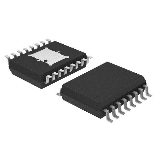
| 产品图片 |
|
| rohs | 符合RoHS无铅 / 符合限制有害物质指令(RoHS)规范要求 |
| 产品系列 | 电源管理 IC,低压差稳压器,Texas Instruments TPS73201DBVR- |
| 数据手册 | |
| 产品型号 | TPS73201DBVR |
| PCN设计/规格 | |
| 产品培训模块 | http://www.digikey.cn/PTM/IndividualPTM.page?site=cn&lang=zhs&ptm=25755 |
| 产品种类 | 低压差稳压器 |
| 供应商器件封装 | SOT-23-5 |
| 其它名称 | 296-32554-1 |
| 制造商产品页 | http://www.ti.com/general/docs/suppproductinfo.tsp?distId=10&orderablePartNumber=TPS73201DBVR |
| 包装 | 剪切带 (CT) |
| 参考电压 | 1.2 V |
| 商标 | Texas Instruments |
| 回动电压—最大值 | 150 mV at 250 mA |
| 安装类型 | 表面贴装 |
| 安装风格 | SMD/SMT |
| 封装 | Reel |
| 封装/外壳 | SC-74A,SOT-753 |
| 封装/箱体 | SOT-23-5 |
| 工作温度 | -40°C ~ 125°C |
| 工厂包装数量 | 3000 |
| 最大功率耗散 | 0.56 W |
| 最大工作温度 | + 125 C |
| 最大输入电压 | 5.5 V |
| 最小工作温度 | - 40 C |
| 最小输入电压 | + 1.7 V |
| 标准包装 | 1 |
| 电压-跌落(典型值) | 0.04V @ 250mA |
| 电压-输入 | 1.7 V ~ 5.5 V |
| 电压-输出 | 1.2 V ~ 5.5 V |
| 电压调节准确度 | 0.5 % |
| 电流-输出 | 250mA |
| 电流-限制(最小值) | 250mA |
| 稳压器拓扑 | 正,可调式 |
| 稳压器数 | 1 |
| 类型 | Low Dropout Regulator with Reverse Current Protection |
| 系列 | TPS73201 |
| 线路调整率 | 0.01 % / V |
| 设计资源 | http://www.digikey.com/product-highlights/cn/zh/texas-instruments-webench-design-center/3176 |
| 负载调节 | 0.002 % / mA |
| 输入偏压电流—最大 | 0.4 mA |
| 输出电压 | 1.2 V to 5.5 V |
| 输出电流 | 250 mA |
| 输出端数量 | 1 Output |
| 输出类型 | Adjustable |


- 商务部:美国ITC正式对集成电路等产品启动337调查
- 曝三星4nm工艺存在良率问题 高通将骁龙8 Gen1或转产台积电
- 太阳诱电将投资9.5亿元在常州建新厂生产MLCC 预计2023年完工
- 英特尔发布欧洲新工厂建设计划 深化IDM 2.0 战略
- 台积电先进制程称霸业界 有大客户加持明年业绩稳了
- 达到5530亿美元!SIA预计今年全球半导体销售额将创下新高
- 英特尔拟将自动驾驶子公司Mobileye上市 估值或超500亿美元
- 三星加码芯片和SET,合并消费电子和移动部门,撤换高东真等 CEO
- 三星电子宣布重大人事变动 还合并消费电子和移动部门
- 海关总署:前11个月进口集成电路产品价值2.52万亿元 增长14.8%


PDF Datasheet 数据手册内容提取
Product Sample & Technical Tools & Support & Folder Buy Documents Software Community TPS732 SBVS037P–AUGUST2003–REVISEDDECEMBER2015 TPS732xx Capacitor-Free, NMOS, 250-mA Low-Dropout Regulator With Reverse Current Protection 1 Features 3 Description • StablewithNoOutputCapacitororAnyValueor The TPS732 family of low-dropout (LDO) voltage 1 regulators uses an NMOS pass element in a voltage- TypeofCapacitor follower configuration. This topology is stable using • InputVoltageRange:1.7Vto5.5V output capacitors with low equivalent series • UltralowDropoutVoltage:40mVTypicalat resistance (ESR), and even allows operation without 250mA a capacitor. The device also provides high reverse blockage(lowreversecurrent)andgroundpincurrent • ExcellentLoadTransientResponse—Withor that is nearly constant over all values of output WithoutOptionalOutputCapacitor current. • NMOSTopologyProvidesLowReverseLeakage Current The TPS732 uses an advanced BiCMOS process to yield high precision while delivering very low dropout • LowNoise:30 μV Typical(10kHzto100kHz) RMS voltages and low ground pin current. Current • 0.5%InitialAccuracy consumption, when not enabled, is less than 1 μA • 1%OverallAccuracy(Line,Load,and and ideal for portable applications. The extremely low Temperature) output noise (30 μVRMS with 0.1-μF CNR) is ideal for powering VCOs. These devices are protected by • LessThan1-μAMaximumI inShutdownMode Q thermalshutdownandfoldbackcurrentlimit. • ThermalShutdownandSpecifiedMinandMax CurrentLimitProtection DeviceInformation(1) • AvailableinMultipleOutputVoltageVersions PARTNUMBER PACKAGE BODYSIZE(NOM) – FixedOutputsof1.2Vto5V SOT-23(5) 2.90mm×1.60mm – AdjustableOutputsfrom1.2Vto5.5V TPS732xx SOT-223(6) 6.50mm×3.50mm – CustomOutputsAvailable SON(8) 3.00mm×3.00mm (1) For all available packages, see the orderable addendum at 2 Applications theendofthedatasheet. • PortableandBattery-PoweredEquipment • Post-RegulationforSwitchingSupplies • Noise-SensitiveCircuitrysuchasVCOs • Point-of-LoadRegulationforDSPs,FPGAs, ASICs,andMicroprocessors TypicalApplicationCircuitforFixed-VoltageVersions Optional Optional VIN IN OUT VOUT TPS732xx EN GND NR ON OFF Optional 1 An IMPORTANT NOTICE at the end of this data sheet addresses availability, warranty, changes, use in safety-critical applications, intellectualpropertymattersandotherimportantdisclaimers.PRODUCTIONDATA.
TPS732 SBVS037P–AUGUST2003–REVISEDDECEMBER2015 www.ti.com Table of Contents 1 Features.................................................................. 1 8 ApplicationandImplementation........................ 16 2 Applications........................................................... 1 8.1 ApplicationInformation............................................16 3 Description............................................................. 1 8.2 TypicalApplications................................................16 4 RevisionHistory..................................................... 2 9 PowerSupplyRecommendations...................... 19 5 PinConfigurationandFunctions......................... 3 10 Layout................................................................... 19 6 Specifications......................................................... 4 10.1 LayoutGuidelines.................................................19 6.1 AbsoluteMaximumRatings......................................4 10.2 LayoutExamples...................................................19 6.2 ESDRatings ............................................................4 10.3 ThermalConsiderations........................................20 6.3 RecommendedOperatingConditions.......................4 11 DeviceandDocumentationSupport................. 22 6.4 ThermalInformation..................................................5 11.1 DeviceSupport......................................................22 6.5 ElectricalCharacteristics...........................................6 11.2 DocumentationSupport .......................................22 6.6 SwitchingCharacteristics..........................................6 11.3 RelatedLinks........................................................22 6.7 TypicalCharacteristics..............................................7 11.4 CommunityResources..........................................23 7 DetailedDescription............................................ 12 11.5 Trademarks...........................................................23 7.1 Overview.................................................................12 11.6 ElectrostaticDischargeCaution............................23 7.2 FunctionalBlockDiagrams.....................................12 11.7 Glossary................................................................23 7.3 FeatureDescription.................................................13 12 Mechanical,Packaging,andOrderable Information........................................................... 23 7.4 DeviceFunctionalModes........................................15 4 Revision History NOTE:Pagenumbersforpreviousrevisionsmaydifferfrompagenumbersinthecurrentversion. ChangesfromRevisionO(August2010)toRevisionP Page • ChangedFeaturesbulletaboutNMOStopology;deleted"new"............................................................................................ 1 • AddedESDRatingstable,FeatureDescriptionsection,DeviceFunctionalModes,ApplicationandImplementation section,PowerSupplyRecommendationssection,Layoutsection,DeviceandDocumentationSupportsection,and Mechanical,Packaging,andOrderableInformationsection ................................................................................................. 1 • ChangedfirstparagraphofDescriptionsection;deleteddescriptionofNMOStopologyas"new"....................................... 1 • ChangedPinConfigurationandFunctionssection;updatedtableformat ............................................................................ 3 • Changed"free-airtemperature"to"junctiontemperature"inAbsoluteMaximumRatingsconditionstatement ...................4 • ChangedThermalInformationtable;updatedthermalresistancevaluesforallpackages .................................................. 5 ChangesfromRevisionN(August,2009)toRevisionO Page • ReplacedtheDissipationRatingstablewiththeThermalInformationtable.......................................................................... 6 ChangesfromRevisionM(May,2008)toRevisionN Page • ChangedFigure10 ................................................................................................................................................................ 7 • Addedparagraphaboutrecommendedstart-upsequencetoInternalCurrentLimitsection.............................................. 14 • Addedparagraphaboutcurrentfoldbackanddevicestart-uptoEnablePinandShutdownsection.................................. 14 2 SubmitDocumentationFeedback Copyright©2003–2015,TexasInstrumentsIncorporated ProductFolderLinks:TPS732
TPS732 www.ti.com SBVS037P–AUGUST2003–REVISEDDECEMBER2015 5 Pin Configuration and Functions DBVPackage DCQPackage 5-PinSOT-23 6-PinSOT-223 TopView TopView IN 1 5 OUT 6 TAB IS GND GND 2 EN 3 4 NR/FB 1 2 3 4 5 IN GND EN OUT NR/FB DRBPackage 8-PinSONWithExposedThermalPad TopView OUT 1 8 IN N/C 2 7 N/C NR/FB 3 6 N/C GND 4 5 EN PinFunctions PIN NO. I/O DESCRIPTION NAME SOT-23 SOT-223 SON IN 1 1 8 I Inputsupply GND 2 3,6 4,Pad — Ground Drivingtheenablepin(EN)highturnsontheregulator.Drivingthispinlowputs EN 3 5 5 I theregulatorintoshutdownmode.RefertotheShutdownsectionunderFeature Descriptionformoredetails.ENcanbeconnectedtoINifnotused. Fixedvoltageversionsonly—connectinganexternalcapacitortothispinbypasses NR 4 4 3 — noisegeneratedbytheinternalbandgap,reducingoutputnoisetoverylowlevels. Adjustablevoltageversiononly—thispinistheinputtothecontrollooperror FB 4 4 3 I amplifier,andisusedtosettheoutputvoltageofthedevice. OUT 5 2 1 O Outputoftheregulator.Therearenooutputcapacitorrequirementsforstability. Copyright©2003–2015,TexasInstrumentsIncorporated SubmitDocumentationFeedback 3 ProductFolderLinks:TPS732
TPS732 SBVS037P–AUGUST2003–REVISEDDECEMBER2015 www.ti.com 6 Specifications 6.1 Absolute Maximum Ratings overoperatingjunctiontemperaturerange(unlessotherwisenoted) (1) MIN MAX UNIT V –0.3 6 IN V –0.3 6 EN Voltage V V –0.3 5.5 OUT V ,V –0.3 6 NR FB Peakoutputcurrent I Internallylimited OUT Outputshort-circuitduration Indefinite Continuoustotalpowerdissipation SeePowerDissipation Junctionrange,T –55 150 J Temperature °C Storagerange,T –65 150 stg (1) StressesbeyondthoselistedunderAbsoluteMaximumRatingsmaycausepermanentdamagetothedevice.Thesearestressratings only,whichdonotimplyfunctionaloperationofthedeviceattheseoranyotherconditionsbeyondthoseindicatedunderRecommended OperatingConditions.Exposuretoabsolute-maximum-ratedconditionsforextendedperiodsmayaffectdevicereliability. 6.2 ESD Ratings VALUE UNIT Humanbodymodel(HBM),perANSI/ESDA/JEDECJS-001,allpins(1) ±2000 V(ESD) Electrostaticdischarge Chargeddevicemodel(CDM),perJEDECspecificationJESD22-C101, V allpins(2) ±500 (1) JEDECdocumentJEP155statesthat500-VHBMallowssafemanufacturingwithastandardESDcontrolprocess. (2) JEDECdocumentJEP157statesthat250-VCDMallowssafemanufacturingwithastandardESDcontrolprocess. 6.3 Recommended Operating Conditions overoperatingjunctiontemperaturerange(unlessotherwisenoted). MIN NOM MAX UNIT V Inputsupplyvoltagerange 1.7 5.5 V IN I Outputcurrent 0 250 mA OUT T Operatingjunctiontemperature –40 125 °C J 4 SubmitDocumentationFeedback Copyright©2003–2015,TexasInstrumentsIncorporated ProductFolderLinks:TPS732
TPS732 www.ti.com SBVS037P–AUGUST2003–REVISEDDECEMBER2015 6.4 Thermal Information TPS732(3) THERMALMETRIC(1)(2) DRB[SON] DCQ DBV[SOT23] UNIT [SOT223] 8PINS 6PINS 5PINS R Junction-to-ambientthermalresistance 58.3 53.1 205.9 θJA R Junction-to-case(top)thermalresistance 93.8 35.2 119 θJC(top) R Junction-to-boardthermalresistance 72.8 7.8 35.4 θJB °C/W ψ Junction-to-topcharacterizationparameter 2.7 2.9 12.7 JT ψ Junction-to-boardcharacterizationparameter 25 7.7 34.5 JB R Junction-to-case(bottom)thermalresistance 5 N/A N/A θJC(bot) (1) Formoreinformationabouttraditionalandnewthermalmetrics,seetheICPackageThermalMetricsapplicationreport,SPRA953. (2) ForthermalestimatesofthisdevicebasedonPCBcopperarea,seetheTIPCBThermalCalculator. (3) ThermaldatafortheDRB,DCQ,andDRVpackagesarederivedbythermalsimulationsbasedonJEDEC-standardmethodologyas specifiedintheJESD51series.Thefollowingassumptionsareusedinthesimulations: (a) i. DRB: The exposed pad is connected to the PCB ground layer through a 2 × 2 thermal via array. . ii. DCQ: The exposed pad is connected to the PCB ground layer through a 3 × 2 thermal via array. .iii.DBV:ThereisnoexposedpadwiththeDBVpackage. (b) i.DRB:Thetopandbottomcopperlayersareassumedtohavea20%thermalconductivityofcopperrepresentinga20%copper coverage. . ii. DCQ: Each of top and bottom copper layers has a dedicated pattern for 20% copper coverage. .iii.DBV:Thetopandbottomcopperlayersareassumedtohavea20%thermalconductivityofcopperrepresentinga20%copper coverage. (c)ThesedataweregeneratedwithonlyasingledeviceatthecenterofaJEDEChigh-K(2s2p)boardwith3-inch×3-inchcopperarea. Tounderstandtheeffectsofthecopperareaonthermalperformance,seethePowerDissipationsectionofthisdatasheet. Copyright©2003–2015,TexasInstrumentsIncorporated SubmitDocumentationFeedback 5 ProductFolderLinks:TPS732
TPS732 SBVS037P–AUGUST2003–REVISEDDECEMBER2015 www.ti.com 6.5 Electrical Characteristics Overoperatingtemperaturerange(T =–40°Cto125°C),V =V +0.5V(1),I =10mA,V =1.7V,andC = J IN OUT(nom) OUT EN OUT 0.1μF,unlessotherwisenoted.TypicalvaluesareatT =25°C. J PARAMETER TESTCONDITIONS MIN TYP MAX UNIT V Inputvoltagerange(1) 1.7 5.5 V IN V Internalreference(TPS73201) T =25°C 1.198 1.2 1.21 V FB J Outputvoltagerange(TPS73201)(2) V 5.5–V V FB DO Nominal T =25°C –0.5% 0.5% V J OUT Accuracy(1)(3) V +0.5V≤V ≤5.5V; V ,I ,andT OUT IN –1% ±0.5% 1% IN OUT 10mA≤I ≤250mA OUT ΔV Lineregulation(1) V +0.5V≤V ≤5.5V 0.01 %/V OUT(ΔVIN) OUT(nom) IN 1mA≤I ≤250mA 0.002 %/mA OUT ΔV Loadregulation OUT(ΔIOUT) 10mA≤I ≤250mA 0.0005 %/mA OUT Dropoutvoltage(4) V I =250mA 40 150 mV DO (V =V (nom)–0.1V) OUT IN OUT Z Outputimpedanceindropout 1.7V≤V ≤V +V 0.25 Ω O(do) IN OUT DO I Outputcurrentlimit V =0.9×V 250 425 600 mA CL OUT OUT(nom) I Short-circuitcurrent V =0V 300 mA SC OUT I Reverseleakagecurrent(5)(–I ) V ≤0.5V,0V≤V ≤V 0.1 10 μA REV IN EN IN OUT I =10mA(I ) 400 550 OUT Q I GNDpincurrent μA GND I =250mA 650 950 OUT V ≤0.5V,V ≤V ≤5.5, I Shutdowncurrent(I ) EN OUT IN 0.02 1 µA SHDN GND –40°C≤T ≤100°C J I FBpincurrent(TPS73201) 0.1 0.3 μA FB Power-supplyrejectionratio f=100Hz,IOUT=250mA 58 PSRR dB (ripplerejection) f=10kHz,I =250mA 37 OUT Outputnoisevoltage COUT=10μF,NoCNR 27×VOUT V μV n BW=10Hz–100kHz C =10μF,C =0.01μF 8.5×V RMS OUT NR OUT V ENpinhigh(enabled) 1.7 V V EN(high) IN V ENpinlow(shutdown) 0 0.5 V EN(low) I ENpincurrent(enabled) V =5.5V 0.02 0.1 μA EN(high) EN Shutdown Tempincreasing 160 T Thermalshutdowntemperature °C SD Reset Tempdecreasing 140 T Operatingjunctiontemperature –40 125 °C J (1) MinimumV =V +V or1.7V,whicheverisgreater. IN OUT DO (2) TPS73201istestedatV =2.5V. OUT (3) Toleranceofexternalresistorsnotincludedinthisspecification. (4) V isnotmeasuredforfixedoutputversionswithV <1.8VbecauseminimumV =1.7V. DO OUT(nom) IN (5) Fixed-voltageversionsonly;refertoApplicationInformationsectionformoreinformation. 6.6 Switching Characteristics overoperatingfree-airtemperaturerange(unlessotherwisenoted) PARAMETER TESTCONDITIONS MIN TYP MAX UNIT V =3V,R =30Ω 600 t Start-uptime OUT L μs STR C =1μF,C =0.01μF OUT NR 6 SubmitDocumentationFeedback Copyright©2003–2015,TexasInstrumentsIncorporated ProductFolderLinks:TPS732
TPS732 www.ti.com SBVS037P–AUGUST2003–REVISEDDECEMBER2015 6.7 Typical Characteristics ForallvoltageversionsatT =25°C,V =V +0.5V,I =10mA,V =1.7V,andC =0.1μF,unlessotherwise J IN OUT(nom) OUT EN OUT noted. 0.5 0.20 0.4 ReferredtoIOUT=10mA 0.15 ReferredtoVIN=VOUT+0.5VatIOUT=10mA 0.3 -40°C (%)UT 00..21 ++21255°C°C (%)UT 00..1005 +125°C +25°C O O V V n 0 n 0 ngei -0.1 ngei -0.05 ha -0.2 ha -40°C C C -0.10 -0.3 -0.4 -0.15 -0.5 -0.20 0 50 100 150 200 250 0 0.5 1.0 1.5 2.0 2.5 3.0 3.5 4.0 4.5 IOUT(mA) VIN-VOUT(V) Figure1.LoadRegulation Figure2.LineRegulation 100 100 TPS73225DBV TPS73225DBV I =250mA OUT 80 80 +125°C V) 60 V) 60 m m V(DO 40 +25°C V(DO 40 20 20 -40°C 0 0 0 50 100 150 200 250 -50 -25 0 25 50 75 100 125 IOUT(mA) Temperature(°C) Figure3. DropoutVoltagevsOutputCurrent Figure4.DropoutVoltagevsTemperature 30 18 I =10mA I =10mA OUT OUT 16 AllVoltageVersions 25 14 %) %) ( 20 ( 12 s s Unit Unit 10 of 15 of 8 nt nt e e erc 10 erc 6 P P 4 5 2 0 0 098765432101234567890 000000000000000000000 -1.-0.-0.-0.-0.-0.-0.-0.-0.-0. 0.0.0.0.0.0.0.0.0.1. -10-9-8-7-6-5-4-3-2-1 12345678910 V Error(%) WorstCasedV /dT(ppm/°C) OUT OUT Figure5.OutputVoltageAccuracyHistogram Figure6.OutputVoltageDriftHistogram Copyright©2003–2015,TexasInstrumentsIncorporated SubmitDocumentationFeedback 7 ProductFolderLinks:TPS732
TPS732 SBVS037P–AUGUST2003–REVISEDDECEMBER2015 www.ti.com Typical Characteristics (continued) ForallvoltageversionsatT =25°C,V =V +0.5V,I =10mA,V =1.7V,andC =0.1μF,unlessotherwise J IN OUT(nom) OUT EN OUT noted. 1000 800 I =250mA 900 700 OUT 800 600 700 500 A) 600 A) m m ( 500 ( 400 D D N N G400 G I I 300 300 V =5.5V 200 VIN=5.5V 200 VIINN=4 V VIN=4 V 100 VIN=2 V 100 V =2 V IN 0 0 0 50 100 150 200 250 -50 -25 0 25 50 75 100 125 IOUT(mA) Temperature(°C) Figure7.GroundPinCurrentvsOutputCurrent Figure8. GroundPinCurrentvsTemperature 1 500 VENABLE=0.5V 450 I V =V +0.5V CL IN OUT 400 A) 350 m m(A)ND0.1 Current ( 320500 ISC IG ut 200 p ut 150 O 100 50 TPS73233 0.01 0 -50 -25 0 25 50 75 100 125 -0.5 0 0.5 1.0 1.5 2.0 2.5 3.0 3.5 Temperature(°C) Output Voltage (V) Figure9. GroundPinCurrentinShutdownvsTemperature Figure10. CurrentLimitvsVOUT(Foldback) 600 600 550 550 A) 500 A) 500 m m mit( 450 mit( 450 Li Li Current 430500 Current 430500 300 300 250 250 1.5 2.0 2.5 3.0 3.5 4.0 4.5 5.0 5.5 -50 -25 0 25 50 75 100 125 VIN(V) Temperature(°C) Figure11. CurrentLimitvsV Figure12. CurrentLimitvsTemperature IN 8 SubmitDocumentationFeedback Copyright©2003–2015,TexasInstrumentsIncorporated ProductFolderLinks:TPS732
TPS732 www.ti.com SBVS037P–AUGUST2003–REVISEDDECEMBER2015 Typical Characteristics (continued) ForallvoltageversionsatT =25°C,V =V +0.5V,I =10mA,V =1.7V,andC =0.1μF,unlessotherwise J IN OUT(nom) OUT EN OUT noted. 90 40 I =100mA I =1 mA 80 COOUUTT=Any COOUUTT=1mF 35 70 B) IOUT=1 mA 30 Rejection(d 654000 ICOOUUTT==1A mnyA COUT=10mF IO=CO10=01mmFA SRR (dB) 2250 e P 15 pl 30 Rip 20 IOUT=100mA 10 FCrOeUqTu=e n1c0y m=F 10 kHz 10 IOUT=Any COUT=10mF 5 VOUT= 2.5 V 0 VIN=VOUT+1 V COUT=0mF 0 IOUT= 100 mA 10 100 1k 10k 100k 1M 10M 0 0.2 0.4 0.6 0.8 1.0 1.2 1.4 1.6 1.8 2.0 Frequency(Hz) VIN-VOUT(V) Figure13.PSRR(RippleRejection)vsFrequency Figure14. PSRR(RippleRejection)vs(VIN–VOUT) 1 1 C =1mF OUT √Hz) COUT=0mF √Hz) COUT=1mF V/ 0.1 V/ 0.1 m C =10mF m ( OUT ( N N e e C =0mF OUT C =10mF OUT IOUT=150 mA IOUT=150 mA 0.01 0.01 10 100 1k 10k 100k 10 100 1k 10k 100k Frequency(Hz) Frequency(Hz) Figure15.NoiseSpectralDensityC =0µF Figure16.NoiseSpectralDensityC =0.01µF NR NR 60 140 V =5.0V OUT 50 120 V =5.0V OUT 100 40 MS) MS) 80 VOUT=3.3V (RN 30 VOUT=3.3V (RN 60 V V 20 40 V =1.5V V =1.5V OUT OUT 10 20 CNR=0.01mF COUT=0mF 10Hz<Frequency<100kHz 10Hz<Frequency<100kHz 0 0 0.1 1 10 1p 10p 100p 1n 10n C (mF) C (F) OUT NR Figure17. RMSNoiseVoltagevsC Figure18. RMSNoiseVoltagevsC OUT NR Copyright©2003–2015,TexasInstrumentsIncorporated SubmitDocumentationFeedback 9 ProductFolderLinks:TPS732
TPS732 SBVS037P–AUGUST2003–REVISEDDECEMBER2015 www.ti.com Typical Characteristics (continued) ForallvoltageversionsatT =25°C,V =V +0.5V,I =10mA,V =1.7V,andC =0.1μF,unlessotherwise J IN OUT(nom) OUT EN OUT noted. VIN=3.8V COUT=0mF IOUT=250mA 50mV/tick V OUT COUT=0mF 50mV/div V COUT=1mF OUT 50mV/tick V OUT 50mV/tick COUT=10mF V 50mV/div COUT=100mF V OUT OUT dV 250mA 5.5V IN=0.5V/ms dt 50mA/tick 4.5V 10mA I 1V/div VIN OUT 10ms/div 10ms/div Figure19.TPS73233LoadTransientResponse Figure20.TPS73233LineTransientResponse RCLOU=T1= k0(cid:3)WmF VOUT RCLOU=T2=0(cid:3)1W0(cid:3)(cid:3)mF 1V/div RCLOU=T2=0(cid:3)(cid:3)1W(cid:3)mF 1V/div RCLOU=T2=0(cid:3)(cid:3)1WmF RCLOU=T2=0(cid:3)(cid:3)1W0(cid:3)mF RCLOU=T1=k0WmF V OUT 2V 2V V EN 1V/div 1V/div 0V 0V V EN 100ms/div 100ms/div Figure21.TPS73233TurnonResponse Figure22.TPS73233TurnoffResponse 6 10 5 V IN 4 V OUT 1 3 A) n Volts 2 (BLE A 1 EN I 0.1 0 -1 -2 0.01 50 ms/div -50 -25 0 25 50 75 100 125 Temperature (°C) . Figure23.TPS73233PowerUpandPowerDown Figure24.IENABLEvsTemperature 10 SubmitDocumentationFeedback Copyright©2003–2015,TexasInstrumentsIncorporated ProductFolderLinks:TPS732
TPS732 www.ti.com SBVS037P–AUGUST2003–REVISEDDECEMBER2015 Typical Characteristics (continued) ForallvoltageversionsatT =25°C,V =V +0.5V,I =10mA,V =1.7V,andC =0.1μF,unlessotherwise J IN OUT(nom) OUT EN OUT noted. 60 160 55 140 50 120 45 100 V(rms)N 4305 I(nA)FB 8600 V =2.5V 30 OUT 40 C =0mF OUT 25 R1=39.2kW 20 10Hz<Frequency<100kHz 20 0 10p 100p 1n 10n -50 -25 0 25 50 75 100 125 C (F) Temperature(°C) FB Figure25.TPS73201RMSNoiseVoltagevsCFB Figure26.TPS73201IFBvsTemperature C =10nF V =2.5V FB OUT 100mV/div R1=39.2kW COUT=0mF VOUT 100mV/div COUT=0mF CFB=10nF VOUT 100mV/div COUT=10mF VOUT 100mV/div COUT=10mF VOUT 4.5V 250mA 3.5V V IN 10mA I OUT 10ms/div 5ms/div Figure27.TPS73201LoadTransient,AdjustableVersion Figure28.TPS73201LineTransient,AdjustableVersion Copyright©2003–2015,TexasInstrumentsIncorporated SubmitDocumentationFeedback 11 ProductFolderLinks:TPS732
TPS732 SBVS037P–AUGUST2003–REVISEDDECEMBER2015 www.ti.com 7 Detailed Description 7.1 Overview The TPS732 family of low-dropout linear regulators operates down to an input voltage of 1.7 V and supports output voltages down to 1.2 V while sourcing up to 500 mA of load current. This linear regulator uses an NMOS pass element with an integrated 4-MHz charge pump to provide a dropout voltage of less than 250 mV at full load current. This unique architecture also permits stable regulation over a wide range of output capacitors. In fact, the TPS732 family of devices does not require any output capacitor for stability. The increased insensitivity to the output capacitor value and type makes this family of linear regulators an ideal choice when powering a loadwheretheeffectivecapacitanceisunknown. The TPS732 family of devices also features a noise reduction (NR) pin that allows for additional reduction of the output noise. With a noise reduction capacitor of 0.01 µF connected from the NR pin to GND, the TPS73215 output noise can be as low as 12.75 µV . The low noise output featured by the TPS732 family makes the RMS devicewell-suitedforpoweringVCOsoranyothernoise-sensitiveload. 7.2 Functional Block Diagrams IN 4MHz ChargePump EN Thermal Protection Ref Servo 27kW Bandgap Error Amp Current Limit OUT 8kW GND R 1 R1+R2=80kW R2 NR Figure29. Fixed-VoltageVersion 12 SubmitDocumentationFeedback Copyright©2003–2015,TexasInstrumentsIncorporated ProductFolderLinks:TPS732
TPS732 www.ti.com SBVS037P–AUGUST2003–REVISEDDECEMBER2015 Functional Block Diagrams (continued) IN Table 1. Standard 1% Resistor Values for Common Output Voltages VO R1 R2 4MHz ChargePump 1.2V Short Open 1.5V 23.2kW 95.3kW EN Thermal 1.8V 28.0kW 56.2kW Protection Ref 2.5V 39.2kW 36.5kW Servo 2.8V 44.2kW 33.2kW 27kW 3.0V 46.4kW 30.9kW Bandgap Error 3.3V 52.3kW 30.1kW Amp OUT NOTE: VOUT= (R1+ R2)/R2´1.204; Current R1úúR2@19kWfor best Limit accuracy. GND 8kW 80kW R 1 FB R 2 Figure30. Adjustable-VoltageVersion 7.3 Feature Description 7.3.1 OutputNoise A precision band-gap reference is used to generate the internal reference voltage, V . This reference is the REF dominant noise source within the TPS732 and it generates approximately 32 µV (10 Hz to 100 kHz) at the RMS reference output (NR). The regulator control loop gains up the reference noise with the same gain as the referencevoltage,sothatthenoisevoltageoftheregulatorisapproximatelygivenby: æR +R2 ö V VN =32mVRMS´çç 1R ÷÷=32mVRMS´ VOUT è 2 ø REF (1) BecausethevalueofV is1.2V,thisrelationshipreducesto: REF æmV ö VN(mVRMS)=27ç RMS ÷´VOUT(V) è V ø (2) An internal 27-kΩ resistor in series with the noise reduction pin (NR) forms a low-pass filter for the voltage reference when an external noise reduction capacitor, C , is connected from NR to ground. For C = 10 nF, NR NR the total noise in the 10-Hz to 100-kHz bandwidth is reduced by a factor of approximately 3.2, giving the approximaterelationship: æmV ö VN(mVRMS)=8.5ç RMS ÷´VOUT(V) è V ø (3) forC =10nF. NR Copyright©2003–2015,TexasInstrumentsIncorporated SubmitDocumentationFeedback 13 ProductFolderLinks:TPS732
TPS732 SBVS037P–AUGUST2003–REVISEDDECEMBER2015 www.ti.com Feature Description (continued) This noise reduction effect is shown as RMS Noise Voltage vs C (Figure 18) in the Typical Characteristics NR section. The TPS73201 adjustable version does not have the NR pin available. However, connecting a feedback capacitor, C , from the output to the feedback pin (FB) reduces output noise and improve load transient FB performance. The TPS732 uses an internal charge pump to develop an internal supply voltage sufficient to drive the gate of the NMOS pass element above V . The charge pump generates approximately 250 μV of switching noise at OUT approximately 4 MHz; however, charge-pump noise contribution is negligible at the output of the regulator for mostvaluesofI andC . OUT OUT 7.3.2 InternalCurrentLimit The TPS732 internal current limit helps protect the regulator during fault conditions. Foldback current limit helps to protect the regulator from damage during output short-circuit conditions by reducing current limit when V OUT dropsbelow0.5V.SeeFigure10intheTypicalCharacteristicssectionforagraphofI vsV . OUT OUT Note from Figure 10 that approximately –0.2 V of V results in a current limit of 0 mA. Therefore, if OUT is OUT forced below –0.2 V before EN goes high, the device may not start up. In applications that work with both a positiveandnegativevoltagesupply,the TPS732shouldbeenabledfirst. 7.3.3 EnablePinandShutdown The enable pin (EN) is active high and is compatible with standard TTL-CMOS levels. A V below 0.5 V EN (maximum) turns the regulator off and drops the GND pin current to approximately 10 nA. When EN is used to shut down the regulator, all charge is removed from the pass transistor gate, and the output ramps back up to a regulatedV (seeFigure21). OUT When shutdown capability is not required, EN can be connected to V . However, the pass gate may not be IN discharged using this configuration, and the pass transistor may be left on (enhanced) for a significant time after V hasbeenremoved.Thisscenariocanresultinreversecurrentflow(iftheINpinislowimpedance)andfaster IN ramp times upon power up. In addition, for V ramp times slower than a few milliseconds, the output may IN overshootuponpowerup. Note that current limit foldback can prevent device start-up under some conditions. See the Internal Current Limit section. 7.3.4 DropoutVoltage TheTPS732usesanNMOSpasstransistortoachieveextremelylowdropout.When(V –V )islessthanthe IN OUT dropout voltage (V ), the NMOS pass device is in its linear region of operation and the input-to-output DO resistanceistheR oftheNMOSpasselement. DS(on) For large step changes in load current, the TPS732 requires a larger voltage drop from V to V to avoid IN OUT degraded transient response. The boundary of this transient dropout region is approximately twice the DC dropout.Valuesof(V –V )abovethislineensurenormaltransientresponse. IN OUT Operating in the transient dropout region can cause an increase in recovery time. The time required to recover from a load transient is a function of the magnitude of the change in load current rate, the rate of change in load current, and the available headroom (V to V voltage drop). Under worst-case conditions [full-scale IN OUT instantaneous load change with (V – V ) close to DC dropout levels], the TPS732 can take a couple of IN OUT hundredmicrosecondstoreturntothespecifiedregulationaccuracy. 14 SubmitDocumentationFeedback Copyright©2003–2015,TexasInstrumentsIncorporated ProductFolderLinks:TPS732
TPS732 www.ti.com SBVS037P–AUGUST2003–REVISEDDECEMBER2015 Feature Description (continued) 7.3.5 ReverseCurrent The NMOS pass element of the TPS732 provides inherent protection against current flow from the output of the regulator to the input when the gate of the pass device is pulled low. To ensure that all charge is removed from the gate of the pass element, the EN pin must be driven low before the input voltage is removed. If this is not done,thepasselementmaybeleftonduetostoredchargeonthegate. After the EN pin is driven low, no bias voltage is needed on any pin for reverse current blocking. Reverse current is specified as the current flowing out of the IN pin due to voltage applied on the OUT pin. Additional current will flowintotheOUTpinduetothe80-kΩ internalresistordividertoground(seeFigure29andFigure30). FortheTPS73201,reversecurrentmayflowwhenV ismorethan1VaboveV . FB IN 7.4 Device Functional Modes 7.4.1 NormalOperationWith1.7V ≤ V ≤5.5VandV ≥ 1.7V IN EN The TPS732 family requires an input voltage of at least 1.7 V to function properly and attempt to maintain regulation. When operating the device near 5.5 V, take care to suppress any transient spikes that may exceed the 6-V absolutemaximumvoltagerating.ThedeviceshouldneveroperateataDCvoltagegreaterthan5.5V. Copyright©2003–2015,TexasInstrumentsIncorporated SubmitDocumentationFeedback 15 ProductFolderLinks:TPS732
TPS732 SBVS037P–AUGUST2003–REVISEDDECEMBER2015 www.ti.com 8 Application and Implementation NOTE Information in the following applications sections is not part of the TI component specification, and TI does not warrant its accuracy or completeness. TI’s customers are responsible for determining suitability of components for their purposes. Customers should validateandtesttheirdesignimplementationtoconfirmsystemfunctionality. 8.1 Application Information The TPS732 device belongs to a family of LDO regulators that use an NMOS pass transistor to achieve ultra- low-dropout performance, reverse current blockage, and freedom from output capacitor constraints. These features, combined with low noise and an enable input, make the TPS732 ideal for portable applications. This regulator family offers a wide selection of fixed-output voltage versions and an adjustable-output version. All versionshavethermalandovercurrentprotection,includingfoldbackcurrentlimit. 8.2 Typical Applications Figure 31 shows the basic circuit connections for the fixed-voltage models. Figure 32 gives the connections for theadjustable-voltageversion(TPS73201). Optional input capacitor. Optional output capacitor. May improve source May improve load transient, impedance, noise, or PSRR. noise, or PSRR. VIN IN OUT VOUT TPS732xx EN GND NR ON OFF Optional bypass capacitor to reduce output noise. Figure31. TypicalApplicationCircuitforFixed-VoltageVersions Optional input capacitor. Optional output capacitor. May improve source May improve load transient, impedance, noise, or PSRR. noise, or PSRR. VIN IN OUT VOUT TPS73201 R C 1 FB EN GND FB ON R OFF 2 (R +R) Optional capacitor VOUT= 1R 2 x 1.204 reduces output noise 2 and improves transient response. Figure32. TypicalApplicationCircuitforAdjustable-VoltageVersion 16 SubmitDocumentationFeedback Copyright©2003–2015,TexasInstrumentsIncorporated ProductFolderLinks:TPS732
TPS732 www.ti.com SBVS037P–AUGUST2003–REVISEDDECEMBER2015 Typical Applications (continued) 8.2.1 DesignRequirements For best accuracy, make the parallel combination of R and R approximately equal to 19 kΩ. This 19 kΩ, in 1 2 addition to the internal 8-kΩ resistor, presents the same impedance to the error amp as the 27-kΩ bandgap referenceoutput.Thisimpedancehelpscompensateforleakagesintotheerrorampterminals. 8.2.2 DetailedDesignProcedure 8.2.2.1 InputandOutputCapacitorRequirements Although an input capacitor is not required for stability, it is good analog design practice to connect a 0.1-μF to 1-μF, low ESR capacitor across the input supply near the regulator. This capacitor counteracts reactive input sources and improves transient response, noise rejection, and ripple rejection. A higher-value capacitor may be necessary if large, fast rise-time load transients are anticipated or the device is located several inches from the powersource. The TPS732 does not require an output capacitor for stability and has maximum phase margin with no capacitor. Itisdesignedtobestableforallavailabletypesandvaluesofcapacitors.InapplicationswheremultiplelowESR capacitors are in parallel, ringing may occur when the product of C and total ESR drops below 50 nΩF. Total OUT ESR includes all parasitic resistances, including capacitor ESR and board, socket, and solder joint resistance. In mostapplications,thesumofcapacitorESRandtraceresistancemeetsthisrequirement. 8.2.2.2 TransientResponse The low open-loop output impedance provided by the NMOS pass element in a voltage follower configuration allows operation without an output capacitor for many applications. As with any regulator, the addition of a capacitor (nominal value 1 μF) from the OUT pin to ground reduces undershoot magnitude but increases its duration.Intheadjustableversion,theadditionofacapacitor,C ,fromtheOUTpintotheFBpinalsoimproves FB thetransientresponse. The TPS732 does not have active pulldown when the output is overvoltage. This feature allows applications that connect higher voltage sources, such as alternate power supplies, to the output. This feature also results in an output overshoot of several percent if the load current quickly drops to zero when a capacitor is connected to the output. The duration of overshoot can be reduced by adding a load resistor. The overshoot decays at a rate determinedbyoutputcapacitorC andtheinternal/externalloadresistance.Therateofdecayisgivenby: OUT (Fixedvoltageversions) V dV/dt = OUT C ´80kWPR OUT LOAD (4) (Adjustablevoltageversion) V dV/dt = OUT C ´80kWP(R +R )PR OUT 1 2 LOAD (5) Copyright©2003–2015,TexasInstrumentsIncorporated SubmitDocumentationFeedback 17 ProductFolderLinks:TPS732
TPS732 SBVS037P–AUGUST2003–REVISEDDECEMBER2015 www.ti.com Typical Applications (continued) 8.2.3 ApplicationCurves RCLOU=T1= k0(cid:3)WmF VOUT 50mV/tick VIN=3.8V COUT=0mF VOUT 1V/div RCLOU=T2=0(cid:3)(cid:3)1W(cid:3)mF COUT=1mF RL=20(cid:3)(cid:3)W 50mV/tick VOUT COUT=10(cid:3)mF 2V V 50mV/tick COUT=10mF V EN OUT 1V/div 250mA 0V 50mA/tick 10mA I OUT 100ms/div 10ms/div Figure33.TPS73233TurnonResponse Figure34.TPS73233LoadTransientResponse 60 C =10nF FB 55 R1=39.2kW 50 100mV/div COUT=0mF VOUT 45 (rms) 40 100mV/div COUT=10mF VOUT N V 35 V =2.5V 30 OUT C =0mF OUT 250mA 25 R1=39.2kW 10Hz<Frequency<100kHz 10mA 20 IOUT 10p 100p 1n 10n 10ms/div C (F) FB Figure35.TPS73201RMSNoiseVoltagevsCFB Figure36.TPS73201LoadTransient,AdjustableVersion 18 SubmitDocumentationFeedback Copyright©2003–2015,TexasInstrumentsIncorporated ProductFolderLinks:TPS732
TPS732 www.ti.com SBVS037P–AUGUST2003–REVISEDDECEMBER2015 9 Power Supply Recommendations These devices are designed to operate from an input voltage supply range between 1.7 V and 5.5 V. The input voltage range provides adequate headroom in order for the device to have a regulated output. This input supply mustbewellregulated.Iftheinputsupplyisnoisy,additionalinputcapacitorswithlowESRcanhelpimprovethe outputnoiseperformance. 10 Layout 10.1 Layout Guidelines To improve AC performance such as PSRR, output noise, and transient response, TI recommends designing the PCBwithseparategroundplanesforV andV ,witheachgroundplaneconnectedonlyattheGNDpinofthe IN OUT device. In addition, the ground connection for the bypass capacitor should connect directly to the GND pin of the device. Solder pad footprint recommendations for the TPS732 are presented in Application Bulletin Solder Pad RecommendationsforSurface-MountDevices(SBFA015),availablefromtheTIwebsiteatwww.ti.com. 10.2 Layout Examples GND PLANE COUT VIN TPS736xxDRB VOUT 1 8 N/C 2 7 N/C CIN NR/FB 3 6 N/C 4 5 EN CNR GND PLANE Figure37. FixedOutputVoltageOptionLayout(DRBPackage) Copyright©2003–2015,TexasInstrumentsIncorporated SubmitDocumentationFeedback 19 ProductFolderLinks:TPS732
TPS732 SBVS037P–AUGUST2003–REVISEDDECEMBER2015 www.ti.com Layout Examples (continued) GND PLANE COUT VOUT VIN TPS73601DRB 1 8 CFF R1 N/C 2 7 N/C CIN NR/FB 3 6 N/C 4 5 EN R2 GND PLANE Figure38. AdjustableOutputVoltageOptionLayout(DRBPackage) 10.3 Thermal Considerations Thermal protection disables the output when the junction temperature rises to approximately 160°C, allowing the device to cool. When the junction temperature cools to approximately 140°C, the output circuitry is again enabled. Depending on power dissipation, thermal resistance, and ambient temperature, the thermal protection circuit may cycle on and off. This limits the dissipation of the regulator, protecting it from damage due to overheating. Any tendency to activate the thermal protection circuit indicates excessive power dissipation or an inadequate heatsink. For reliable operation, junction temperature should be limited to 125°C maximum. To estimate the margin of safety in a complete design (including heatsink), increase the ambient temperature until the thermal protection is triggered; use worst-case loads and signal conditions. For good reliability, thermal protection should trigger at least 35°C above the maximum expected ambient condition of your application. This produces a worst- casejunctiontemperatureof125°Catthehighestexpectedambienttemperatureandworst-caseload. The internal protection circuitry of the TPS732 has been designed to protect against overload conditions. It was not intended to replace proper heatsinking. Continuously running the TPS732 into thermal shutdown will degrade devicereliability. 20 SubmitDocumentationFeedback Copyright©2003–2015,TexasInstrumentsIncorporated ProductFolderLinks:TPS732
TPS732 www.ti.com SBVS037P–AUGUST2003–REVISEDDECEMBER2015 Thermal Considerations (continued) 10.3.1 PowerDissipation The ability to remove heat from the die is different for each package type, presenting different considerations in the PCB layout. The PCB area around the device that is free of other components moves the heat from the device to the ambient air. Performance data for JEDEC low- and high-K boards are shown in the Thermal Information table. Using heavier copper increases the effectiveness in removing heat from the device. The additionofplatedthrough-holestoheat-dissipatinglayersalsoimprovestheheat-sinkeffectiveness. Powerdissipationdependsoninputvoltageandloadconditions.Powerdissipation(P )isequaltotheproductof D theoutputcurrenttimesthevoltagedropacrosstheoutputpasselement(V toV ): IN OUT P =(V -V )´I D IN OUT OUT (6) Power dissipation can be minimized by using the lowest possible input voltage necessary to assure the required outputvoltage. Copyright©2003–2015,TexasInstrumentsIncorporated SubmitDocumentationFeedback 21 ProductFolderLinks:TPS732
TPS732 SBVS037P–AUGUST2003–REVISEDDECEMBER2015 www.ti.com 11 Device and Documentation Support 11.1 Device Support 11.1.1 DevelopmentSupport 11.1.1.1 EvaluationModules An evaluation module (EVM) is available to assist in the initial circuit performance evaluation using the TPS732. The TPS73201DRBEVM-518 evaluation module (and related user guide) can be requested at the Texas InstrumentswebsitethroughtheproductfoldersorpurchaseddirectlyfromtheTIeStore. 11.1.1.2 SpiceModels Computer simulation of circuit performance using SPICE is often useful when analyzing the performance of analog circuits and systems. A SPICE model for the TPS732 is available through the product folders under SimulationModels. 11.1.2 DeviceNomenclature Table1.DeviceNomenclature(1) PRODUCT V OUT TPS732xxyyyz XXisthenominaloutputvoltage(forexample,25=2.5V;01=Adjustable). YYYisthepackagedesignator. Zisthetapeandreelquantity(R=3000,T=250). (1) ForthemostcurrentpackageandorderinginformationseethePackageOptionAddendumattheendofthisdocument,orseetheTI websiteatwww.ti.com. 11.2 Documentation Support 11.2.1 RelatedDocumentation • RegulatingV Below1.2VUsinganExternalReference,SLVA216 OUT • SolderPadRecommendationsforSurface-MountDevices,SBFA019 • TPS73x01DRBEVM-518User'sGuide,SBVU014 11.3 Related Links The table below lists quick access links. Categories include technical documents, support and community resources,toolsandsoftware,andquickaccesstosampleorbuy. Table2.RelatedLinks TECHNICAL TOOLS& SUPPORT& PARTS PRODUCTFOLDER SAMPLE&BUY DOCUMENTS SOFTWARE COMMUNITY TPS73201 Clickhere Clickhere Clickhere Clickhere Clickhere TPS73213 Clickhere Clickhere Clickhere Clickhere Clickhere TPS73215 Clickhere Clickhere Clickhere Clickhere Clickhere TPS73216 Clickhere Clickhere Clickhere Clickhere Clickhere TPS73218 Clickhere Clickhere Clickhere Clickhere Clickhere TPS73219 Clickhere Clickhere Clickhere Clickhere Clickhere TPS73225 Clickhere Clickhere Clickhere Clickhere Clickhere TPS73230 Clickhere Clickhere Clickhere Clickhere Clickhere TPS73233 Clickhere Clickhere Clickhere Clickhere Clickhere TPS73250 Clickhere Clickhere Clickhere Clickhere Clickhere 22 SubmitDocumentationFeedback Copyright©2003–2015,TexasInstrumentsIncorporated ProductFolderLinks:TPS732
TPS732 www.ti.com SBVS037P–AUGUST2003–REVISEDDECEMBER2015 11.4 Community Resources The following links connect to TI community resources. Linked contents are provided "AS IS" by the respective contributors. They do not constitute TI specifications and do not necessarily reflect TI's views; see TI's Terms of Use. TIE2E™OnlineCommunity TI'sEngineer-to-Engineer(E2E)Community.Createdtofostercollaboration amongengineers.Ate2e.ti.com,youcanaskquestions,shareknowledge,exploreideasandhelp solveproblemswithfellowengineers. DesignSupport TI'sDesignSupport QuicklyfindhelpfulE2Eforumsalongwithdesignsupporttoolsand contactinformationfortechnicalsupport. 11.5 Trademarks E2EisatrademarkofTexasInstruments. Allothertrademarksarethepropertyoftheirrespectiveowners. 11.6 Electrostatic Discharge Caution Thesedeviceshavelimitedbuilt-inESDprotection.Theleadsshouldbeshortedtogetherorthedeviceplacedinconductivefoam duringstorageorhandlingtopreventelectrostaticdamagetotheMOSgates. 11.7 Glossary SLYZ022—TIGlossary. Thisglossarylistsandexplainsterms,acronyms,anddefinitions. 12 Mechanical, Packaging, and Orderable Information The following pages include mechanical, packaging, and orderable information. This information is the most current data available for the designated devices. This data is subject to change without notice and revision of thisdocument.Forbrowser-basedversionsofthisdatasheet,refertotheleft-handnavigation. Copyright©2003–2015,TexasInstrumentsIncorporated SubmitDocumentationFeedback 23 ProductFolderLinks:TPS732
PACKAGE OPTION ADDENDUM www.ti.com 6-Feb-2020 PACKAGING INFORMATION Orderable Device Status Package Type Package Pins Package Eco Plan Lead/Ball Finish MSL Peak Temp Op Temp (°C) Device Marking Samples (1) Drawing Qty (2) (6) (3) (4/5) TPS73201DBVR ACTIVE SOT-23 DBV 5 3000 Green (RoHS NIPDAU Level-1-260C-UNLIM -40 to 125 PJEQ & no Sb/Br) TPS73201DBVRG4 ACTIVE SOT-23 DBV 5 3000 Green (RoHS NIPDAU Level-1-260C-UNLIM -40 to 125 PJEQ & no Sb/Br) TPS73201DBVT ACTIVE SOT-23 DBV 5 250 Green (RoHS NIPDAU Level-1-260C-UNLIM -40 to 125 PJEQ & no Sb/Br) TPS73201DBVTG4 ACTIVE SOT-23 DBV 5 250 Green (RoHS NIPDAU Level-1-260C-UNLIM -40 to 125 PJEQ & no Sb/Br) TPS73201DCQ ACTIVE SOT-223 DCQ 6 78 Green (RoHS NIPDAU Level-2-260C-1 YEAR -40 to 125 PS73201 & no Sb/Br) TPS73201DCQR ACTIVE SOT-223 DCQ 6 2500 Green (RoHS SN Level-2-260C-1 YEAR -40 to 125 PS73201 & no Sb/Br) TPS73201DRBR ACTIVE SON DRB 8 3000 Green (RoHS NIPDAU Level-2-260C-1 YEAR -40 to 125 PJEQ & no Sb/Br) TPS73201DRBRG4 ACTIVE SON DRB 8 3000 Green (RoHS NIPDAU Level-2-260C-1 YEAR -40 to 125 PJEQ & no Sb/Br) TPS73201DRBT ACTIVE SON DRB 8 250 Green (RoHS NIPDAU Level-2-260C-1 YEAR -40 to 125 PJEQ & no Sb/Br) TPS73201DRBTG4 ACTIVE SON DRB 8 250 Green (RoHS NIPDAU Level-2-260C-1 YEAR -40 to 125 PJEQ & no Sb/Br) TPS73213DBVR ACTIVE SOT-23 DBV 5 3000 Green (RoHS NIPDAU Level-1-260C-UNLIM -40 to 125 BWD & no Sb/Br) TPS73213DBVT ACTIVE SOT-23 DBV 5 250 Green (RoHS NIPDAU Level-1-260C-UNLIM -40 to 125 BWD & no Sb/Br) TPS73215DBVR ACTIVE SOT-23 DBV 5 3000 Green (RoHS NIPDAU Level-1-260C-UNLIM -40 to 125 T38 & no Sb/Br) TPS73215DBVT ACTIVE SOT-23 DBV 5 250 Green (RoHS NIPDAU Level-1-260C-UNLIM -40 to 125 T38 & no Sb/Br) TPS73215DCQ ACTIVE SOT-223 DCQ 6 78 Green (RoHS NIPDAU Level-2-260C-1 YEAR -40 to 125 PS73215 & no Sb/Br) TPS73215DCQR ACTIVE SOT-223 DCQ 6 2500 Green (RoHS NIPDAU Level-2-260C-1 YEAR -40 to 125 PS73215 & no Sb/Br) TPS73216DBVT ACTIVE SOT-23 DBV 5 250 Green (RoHS NIPDAU Level-2-260C-1 YEAR -40 to 125 T50 & no Sb/Br) Addendum-Page 1
PACKAGE OPTION ADDENDUM www.ti.com 6-Feb-2020 Orderable Device Status Package Type Package Pins Package Eco Plan Lead/Ball Finish MSL Peak Temp Op Temp (°C) Device Marking Samples (1) Drawing Qty (2) (6) (3) (4/5) TPS73216DBVTG4 ACTIVE SOT-23 DBV 5 250 Green (RoHS NIPDAU Level-2-260C-1 YEAR -40 to 125 T50 & no Sb/Br) TPS73218DBVR ACTIVE SOT-23 DBV 5 3000 Green (RoHS NIPDAU Level-1-260C-UNLIM -40 to 125 T37 & no Sb/Br) TPS73218DBVRG4 ACTIVE SOT-23 DBV 5 3000 Green (RoHS NIPDAU Level-1-260C-UNLIM -40 to 125 T37 & no Sb/Br) TPS73218DBVT ACTIVE SOT-23 DBV 5 250 Green (RoHS NIPDAU Level-1-260C-UNLIM -40 to 125 T37 & no Sb/Br) TPS73218DCQ ACTIVE SOT-223 DCQ 6 78 Green (RoHS NIPDAU Level-2-260C-1 YEAR -40 to 125 PS73218 & no Sb/Br) TPS73218DCQR ACTIVE SOT-223 DCQ 6 2500 Green (RoHS SN Level-2-260C-1 YEAR -40 to 125 PS73218 & no Sb/Br) TPS73219DBVR ACTIVE SOT-23 DBV 5 3000 Green (RoHS NIPDAU Level-1-260C-UNLIM -40 to 125 CGE & no Sb/Br) TPS73219DBVT ACTIVE SOT-23 DBV 5 250 Green (RoHS NIPDAU Level-1-260C-UNLIM -40 to 125 CGE & no Sb/Br) TPS73225DBVR ACTIVE SOT-23 DBV 5 3000 Green (RoHS NIPDAU Level-1-260C-UNLIM -40 to 125 T36 & no Sb/Br) TPS73225DBVT ACTIVE SOT-23 DBV 5 250 Green (RoHS NIPDAU Level-1-260C-UNLIM -40 to 125 T36 & no Sb/Br) TPS73225DBVTG4 ACTIVE SOT-23 DBV 5 250 Green (RoHS NIPDAU Level-1-260C-UNLIM -40 to 125 T36 & no Sb/Br) TPS73225DCQ ACTIVE SOT-223 DCQ 6 78 Green (RoHS NIPDAU Level-2-260C-1 YEAR -40 to 125 PS73225 & no Sb/Br) TPS73225DCQR ACTIVE SOT-223 DCQ 6 2500 Green (RoHS NIPDAU Level-2-260C-1 YEAR -40 to 125 PS73225 & no Sb/Br) TPS73230DBVR ACTIVE SOT-23 DBV 5 3000 Green (RoHS NIPDAU Level-1-260C-UNLIM -40 to 125 T39 & no Sb/Br) TPS73230DBVT ACTIVE SOT-23 DBV 5 250 Green (RoHS NIPDAU Level-1-260C-UNLIM -40 to 125 T39 & no Sb/Br) TPS73230DCQR ACTIVE SOT-223 DCQ 6 2500 Green (RoHS NIPDAU Level-2-260C-1 YEAR -40 to 125 PS73230 & no Sb/Br) TPS73233DBVR ACTIVE SOT-23 DBV 5 3000 Green (RoHS NIPDAU Level-1-260C-UNLIM -40 to 125 T40 & no Sb/Br) TPS73233DBVT ACTIVE SOT-23 DBV 5 250 Green (RoHS NIPDAU Level-1-260C-UNLIM -40 to 125 T40 & no Sb/Br) Addendum-Page 2
PACKAGE OPTION ADDENDUM www.ti.com 6-Feb-2020 Orderable Device Status Package Type Package Pins Package Eco Plan Lead/Ball Finish MSL Peak Temp Op Temp (°C) Device Marking Samples (1) Drawing Qty (2) (6) (3) (4/5) TPS73233DCQ ACTIVE SOT-223 DCQ 6 78 Green (RoHS NIPDAU Level-2-260C-1 YEAR -40 to 125 PS73233 & no Sb/Br) TPS73233DCQR ACTIVE SOT-223 DCQ 6 2500 Green (RoHS SN Level-2-260C-1 YEAR -40 to 125 PS73233 & no Sb/Br) TPS73250DBVR ACTIVE SOT-23 DBV 5 3000 Green (RoHS NIPDAU Level-1-260C-UNLIM -40 to 125 T41 & no Sb/Br) TPS73250DBVT ACTIVE SOT-23 DBV 5 250 Green (RoHS NIPDAU Level-1-260C-UNLIM -40 to 125 T41 & no Sb/Br) TPS73250DCQ ACTIVE SOT-223 DCQ 6 78 Green (RoHS NIPDAU Level-2-260C-1 YEAR -40 to 125 PS73250 & no Sb/Br) TPS73250DCQR ACTIVE SOT-223 DCQ 6 2500 Green (RoHS NIPDAU Level-2-260C-1 YEAR -40 to 125 PS73250 & no Sb/Br) (1) The marketing status values are defined as follows: ACTIVE: Product device recommended for new designs. LIFEBUY: TI has announced that the device will be discontinued, and a lifetime-buy period is in effect. NRND: Not recommended for new designs. Device is in production to support existing customers, but TI does not recommend using this part in a new design. PREVIEW: Device has been announced but is not in production. Samples may or may not be available. OBSOLETE: TI has discontinued the production of the device. (2) RoHS: TI defines "RoHS" to mean semiconductor products that are compliant with the current EU RoHS requirements for all 10 RoHS substances, including the requirement that RoHS substance do not exceed 0.1% by weight in homogeneous materials. Where designed to be soldered at high temperatures, "RoHS" products are suitable for use in specified lead-free processes. TI may reference these types of products as "Pb-Free". RoHS Exempt: TI defines "RoHS Exempt" to mean products that contain lead but are compliant with EU RoHS pursuant to a specific EU RoHS exemption. Green: TI defines "Green" to mean the content of Chlorine (Cl) and Bromine (Br) based flame retardants meet JS709B low halogen requirements of <=1000ppm threshold. Antimony trioxide based flame retardants must also meet the <=1000ppm threshold requirement. (3) MSL, Peak Temp. - The Moisture Sensitivity Level rating according to the JEDEC industry standard classifications, and peak solder temperature. (4) There may be additional marking, which relates to the logo, the lot trace code information, or the environmental category on the device. (5) Multiple Device Markings will be inside parentheses. Only one Device Marking contained in parentheses and separated by a "~" will appear on a device. If a line is indented then it is a continuation of the previous line and the two combined represent the entire Device Marking for that device. (6) Lead/Ball Finish - Orderable Devices may have multiple material finish options. Finish options are separated by a vertical ruled line. Lead/Ball Finish values may wrap to two lines if the finish value exceeds the maximum column width. Addendum-Page 3
PACKAGE OPTION ADDENDUM www.ti.com 6-Feb-2020 Important Information and Disclaimer:The information provided on this page represents TI's knowledge and belief as of the date that it is provided. TI bases its knowledge and belief on information provided by third parties, and makes no representation or warranty as to the accuracy of such information. Efforts are underway to better integrate information from third parties. TI has taken and continues to take reasonable steps to provide representative and accurate information but may not have conducted destructive testing or chemical analysis on incoming materials and chemicals. TI and TI suppliers consider certain information to be proprietary, and thus CAS numbers and other limited information may not be available for release. In no event shall TI's liability arising out of such information exceed the total purchase price of the TI part(s) at issue in this document sold by TI to Customer on an annual basis. OTHER QUALIFIED VERSIONS OF TPS732 : •Automotive: TPS732-Q1 NOTE: Qualified Version Definitions: •Automotive - Q100 devices qualified for high-reliability automotive applications targeting zero defects Addendum-Page 4
PACKAGE MATERIALS INFORMATION www.ti.com 24-Apr-2020 TAPE AND REEL INFORMATION *Alldimensionsarenominal Device Package Package Pins SPQ Reel Reel A0 B0 K0 P1 W Pin1 Type Drawing Diameter Width (mm) (mm) (mm) (mm) (mm) Quadrant (mm) W1(mm) TPS73201DBVR SOT-23 DBV 5 3000 178.0 9.0 3.3 3.2 1.4 4.0 8.0 Q3 TPS73201DBVR SOT-23 DBV 5 3000 180.0 8.4 3.2 3.2 1.4 4.0 8.0 Q3 TPS73201DBVT SOT-23 DBV 5 250 179.0 8.4 3.2 3.2 1.4 4.0 8.0 Q3 TPS73201DBVT SOT-23 DBV 5 250 178.0 9.0 3.23 3.17 1.37 4.0 8.0 Q3 TPS73201DCQR SOT-223 DCQ 6 2500 330.0 12.4 7.1 7.45 1.88 8.0 12.0 Q3 TPS73201DRBR SON DRB 8 3000 330.0 12.4 3.3 3.3 1.1 8.0 12.0 Q2 TPS73201DRBR SON DRB 8 3000 330.0 12.4 3.3 3.3 1.0 8.0 12.0 Q2 TPS73201DRBT SON DRB 8 250 180.0 12.4 3.3 3.3 1.1 8.0 12.0 Q2 TPS73201DRBT SON DRB 8 250 180.0 12.4 3.3 3.3 1.0 8.0 12.0 Q2 TPS73213DBVR SOT-23 DBV 5 3000 178.0 9.0 3.23 3.17 1.37 4.0 8.0 Q3 TPS73213DBVT SOT-23 DBV 5 250 178.0 9.0 3.23 3.17 1.37 4.0 8.0 Q3 TPS73215DBVR SOT-23 DBV 5 3000 178.0 9.0 3.23 3.17 1.37 4.0 8.0 Q3 TPS73215DBVT SOT-23 DBV 5 250 178.0 9.0 3.23 3.17 1.37 4.0 8.0 Q3 TPS73215DCQR SOT-223 DCQ 6 2500 330.0 12.4 7.1 7.45 1.88 8.0 12.0 Q3 TPS73216DBVT SOT-23 DBV 5 250 179.0 8.4 3.2 3.2 1.4 4.0 8.0 Q3 TPS73218DBVR SOT-23 DBV 5 3000 178.0 9.0 3.23 3.17 1.37 4.0 8.0 Q3 TPS73218DBVT SOT-23 DBV 5 250 178.0 9.0 3.23 3.17 1.37 4.0 8.0 Q3 TPS73218DCQR SOT-223 DCQ 6 2500 330.0 12.4 7.1 7.45 1.88 8.0 12.0 Q3 PackMaterials-Page1
PACKAGE MATERIALS INFORMATION www.ti.com 24-Apr-2020 Device Package Package Pins SPQ Reel Reel A0 B0 K0 P1 W Pin1 Type Drawing Diameter Width (mm) (mm) (mm) (mm) (mm) Quadrant (mm) W1(mm) TPS73219DBVR SOT-23 DBV 5 3000 178.0 9.0 3.23 3.17 1.37 4.0 8.0 Q3 TPS73219DBVT SOT-23 DBV 5 250 178.0 9.0 3.23 3.17 1.37 4.0 8.0 Q3 TPS73225DBVR SOT-23 DBV 5 3000 178.0 9.0 3.23 3.17 1.37 4.0 8.0 Q3 TPS73225DBVT SOT-23 DBV 5 250 178.0 9.0 3.23 3.17 1.37 4.0 8.0 Q3 TPS73225DCQR SOT-223 DCQ 6 2500 330.0 12.4 7.1 7.45 1.88 8.0 12.0 Q3 TPS73230DBVR SOT-23 DBV 5 3000 178.0 9.0 3.23 3.17 1.37 4.0 8.0 Q3 TPS73230DBVT SOT-23 DBV 5 250 178.0 9.0 3.23 3.17 1.37 4.0 8.0 Q3 TPS73230DCQR SOT-223 DCQ 6 2500 330.0 12.4 7.1 7.45 1.88 8.0 12.0 Q3 TPS73233DBVR SOT-23 DBV 5 3000 178.0 9.0 3.23 3.17 1.37 4.0 8.0 Q3 TPS73233DBVT SOT-23 DBV 5 250 178.0 9.0 3.23 3.17 1.37 4.0 8.0 Q3 TPS73233DCQR SOT-223 DCQ 6 2500 330.0 12.4 7.1 7.45 1.88 8.0 12.0 Q3 TPS73250DBVR SOT-23 DBV 5 3000 178.0 9.0 3.23 3.17 1.37 4.0 8.0 Q3 TPS73250DBVT SOT-23 DBV 5 250 178.0 9.0 3.23 3.17 1.37 4.0 8.0 Q3 TPS73250DCQR SOT-223 DCQ 6 2500 330.0 12.4 7.1 7.45 1.88 8.0 12.0 Q3 *Alldimensionsarenominal Device PackageType PackageDrawing Pins SPQ Length(mm) Width(mm) Height(mm) TPS73201DBVR SOT-23 DBV 5 3000 180.0 180.0 18.0 TPS73201DBVR SOT-23 DBV 5 3000 203.0 203.0 35.0 TPS73201DBVT SOT-23 DBV 5 250 203.0 203.0 35.0 PackMaterials-Page2
PACKAGE MATERIALS INFORMATION www.ti.com 24-Apr-2020 Device PackageType PackageDrawing Pins SPQ Length(mm) Width(mm) Height(mm) TPS73201DBVT SOT-23 DBV 5 250 180.0 180.0 18.0 TPS73201DCQR SOT-223 DCQ 6 2500 367.0 367.0 35.0 TPS73201DRBR SON DRB 8 3000 367.0 367.0 35.0 TPS73201DRBR SON DRB 8 3000 370.0 355.0 55.0 TPS73201DRBT SON DRB 8 250 210.0 185.0 35.0 TPS73201DRBT SON DRB 8 250 220.0 205.0 50.0 TPS73213DBVR SOT-23 DBV 5 3000 180.0 180.0 18.0 TPS73213DBVT SOT-23 DBV 5 250 180.0 180.0 18.0 TPS73215DBVR SOT-23 DBV 5 3000 180.0 180.0 18.0 TPS73215DBVT SOT-23 DBV 5 250 180.0 180.0 18.0 TPS73215DCQR SOT-223 DCQ 6 2500 346.0 346.0 41.0 TPS73216DBVT SOT-23 DBV 5 250 195.0 200.0 45.0 TPS73218DBVR SOT-23 DBV 5 3000 180.0 180.0 18.0 TPS73218DBVT SOT-23 DBV 5 250 180.0 180.0 18.0 TPS73218DCQR SOT-223 DCQ 6 2500 367.0 367.0 35.0 TPS73219DBVR SOT-23 DBV 5 3000 180.0 180.0 18.0 TPS73219DBVT SOT-23 DBV 5 250 180.0 180.0 18.0 TPS73225DBVR SOT-23 DBV 5 3000 180.0 180.0 18.0 TPS73225DBVT SOT-23 DBV 5 250 180.0 180.0 18.0 TPS73225DCQR SOT-223 DCQ 6 2500 346.0 346.0 41.0 TPS73230DBVR SOT-23 DBV 5 3000 180.0 180.0 18.0 TPS73230DBVT SOT-23 DBV 5 250 180.0 180.0 18.0 TPS73230DCQR SOT-223 DCQ 6 2500 346.0 346.0 41.0 TPS73233DBVR SOT-23 DBV 5 3000 180.0 180.0 18.0 TPS73233DBVT SOT-23 DBV 5 250 180.0 180.0 18.0 TPS73233DCQR SOT-223 DCQ 6 2500 367.0 367.0 35.0 TPS73250DBVR SOT-23 DBV 5 3000 180.0 180.0 18.0 TPS73250DBVT SOT-23 DBV 5 250 180.0 180.0 18.0 TPS73250DCQR SOT-223 DCQ 6 2500 346.0 346.0 41.0 PackMaterials-Page3
None
None
None
PACKAGE OUTLINE DRB0008A VSON - 1 mm max height SCALE 4.000 PLASTIC SMALL OUTLINE - NO LEAD 3.1 B A 2.9 PIN 1 INDEX AREA 3.1 2.9 C 1 MAX SEATING PLANE 0.05 0.08 C DIM A 0.00 OPT 1 OPT 2 1.5 0.1 (0.1) (0.2) 4X (0.23) EXPOSED (DIM A) TYP THERMAL PAD 4 5 2X 1.95 1.75 0.1 8 1 6X 0.65 0.37 8X 0.25 PIN 1 ID 0.1 C A B (OPTIONAL) (0.65) 0.05 C 0.5 8X 0.3 4218875/A 01/2018 NOTES: 1. All linear dimensions are in millimeters. Any dimensions in parenthesis are for reference only. Dimensioning and tolerancing per ASME Y14.5M. 2. This drawing is subject to change without notice. 3. The package thermal pad must be soldered to the printed circuit board for thermal and mechanical performance. www.ti.com
EXAMPLE BOARD LAYOUT DRB0008A VSON - 1 mm max height PLASTIC SMALL OUTLINE - NO LEAD (1.5) (0.65) SYMM 8X (0.6) (0.825) 8X (0.31) 1 8 SYMM (1.75) (0.625) 6X (0.65) 4 5 (R0.05) TYP ( 0.2) VIA TYP (0.23) (0.5) (2.8) LAND PATTERN EXAMPLE EXPOSED METAL SHOWN SCALE:20X 0.07 MAX 0.07 MIN ALL AROUND ALL AROUND EXPOSED EXPOSED METAL METAL SOLDER MASK METAL METAL UNDER SOLDER MASK OPENING SOLDER MASK OPENING NON SOLDER MASK SOLDER MASK DEFINED DEFINED (PREFERRED) SOLDER MASK DETAILS 4218875/A 01/2018 NOTES: (continued) 4. This package is designed to be soldered to a thermal pad on the board. For more information, see Texas Instruments literature number SLUA271 (www.ti.com/lit/slua271). 5. Vias are optional depending on application, refer to device data sheet. If any vias are implemented, refer to their locations shown on this view. It is recommended that vias under paste be filled, plugged or tented. www.ti.com
EXAMPLE STENCIL DESIGN DRB0008A VSON - 1 mm max height PLASTIC SMALL OUTLINE - NO LEAD (0.65) 4X (0.23) SYMM METAL TYP 8X (0.6) 4X (0.725) 8X (0.31) 1 8 (2.674) SYMM (1.55) 6X (0.65) 4 5 (R0.05) TYP (1.34) (2.8) SOLDER PASTE EXAMPLE BASED ON 0.125 mm THICK STENCIL EXPOSED PAD 84% PRINTED SOLDER COVERAGE BY AREA SCALE:25X 4218875/A 01/2018 NOTES: (continued) 6. Laser cutting apertures with trapezoidal walls and rounded corners may offer better paste release. IPC-7525 may have alternate design recommendations. www.ti.com
PACKAGE OUTLINE DBV0005A SOT-23 - 1.45 mm max height SCALE 4.000 SMALL OUTLINE TRANSISTOR C 3.0 2.6 0.1 C 1.75 1.45 1.45 B A 0.90 PIN 1 INDEX AREA 1 5 2X 0.95 3.05 2.75 1.9 1.9 2 4 3 0.5 5X 0.3 0.15 0.2 C A B (1.1) TYP 0.00 0.25 GAGE PLANE 0.22 TYP 0.08 8 TYP 0.6 0 0.3 TYP SEATING PLANE 4214839/E 09/2019 NOTES: 1. All linear dimensions are in millimeters. Any dimensions in parenthesis are for reference only. Dimensioning and tolerancing per ASME Y14.5M. 2. This drawing is subject to change without notice. 3. Refernce JEDEC MO-178. 4. Body dimensions do not include mold flash, protrusions, or gate burrs. Mold flash, protrusions, or gate burrs shall not exceed 0.15 mm per side. www.ti.com
EXAMPLE BOARD LAYOUT DBV0005A SOT-23 - 1.45 mm max height SMALL OUTLINE TRANSISTOR PKG 5X (1.1) 1 5 5X (0.6) SYMM (1.9) 2 2X (0.95) 3 4 (R0.05) TYP (2.6) LAND PATTERN EXAMPLE EXPOSED METAL SHOWN SCALE:15X SOLDER MASK SOLDER MASK METAL UNDER METAL OPENING OPENING SOLDER MASK EXPOSED METAL EXPOSED METAL 0.07 MAX 0.07 MIN ARROUND ARROUND NON SOLDER MASK SOLDER MASK DEFINED DEFINED (PREFERRED) SOLDER MASK DETAILS 4214839/E 09/2019 NOTES: (continued) 5. Publication IPC-7351 may have alternate designs. 6. Solder mask tolerances between and around signal pads can vary based on board fabrication site. www.ti.com
EXAMPLE STENCIL DESIGN DBV0005A SOT-23 - 1.45 mm max height SMALL OUTLINE TRANSISTOR PKG 5X (1.1) 1 5 5X (0.6) SYMM 2 (1.9) 2X(0.95) 3 4 (R0.05) TYP (2.6) SOLDER PASTE EXAMPLE BASED ON 0.125 mm THICK STENCIL SCALE:15X 4214839/E 09/2019 NOTES: (continued) 7. Laser cutting apertures with trapezoidal walls and rounded corners may offer better paste release. IPC-7525 may have alternate design recommendations. 8. Board assembly site may have different recommendations for stencil design. www.ti.com
IMPORTANTNOTICEANDDISCLAIMER TI PROVIDES TECHNICAL AND RELIABILITY DATA (INCLUDING DATASHEETS), DESIGN RESOURCES (INCLUDING REFERENCE DESIGNS), APPLICATION OR OTHER DESIGN ADVICE, WEB TOOLS, SAFETY INFORMATION, AND OTHER RESOURCES “AS IS” AND WITH ALL FAULTS, AND DISCLAIMS ALL WARRANTIES, EXPRESS AND IMPLIED, INCLUDING WITHOUT LIMITATION ANY IMPLIED WARRANTIES OF MERCHANTABILITY, FITNESS FOR A PARTICULAR PURPOSE OR NON-INFRINGEMENT OF THIRD PARTY INTELLECTUAL PROPERTY RIGHTS. These resources are intended for skilled developers designing with TI products. You are solely responsible for (1) selecting the appropriate TI products for your application, (2) designing, validating and testing your application, and (3) ensuring your application meets applicable standards, and any other safety, security, or other requirements. These resources are subject to change without notice. TI grants you permission to use these resources only for development of an application that uses the TI products described in the resource. Other reproduction and display of these resources is prohibited. No license is granted to any other TI intellectual property right or to any third party intellectual property right. TI disclaims responsibility for, and you will fully indemnify TI and its representatives against, any claims, damages, costs, losses, and liabilities arising out of your use of these resources. TI’s products are provided subject to TI’s Terms of Sale (www.ti.com/legal/termsofsale.html) or other applicable terms available either on ti.com or provided in conjunction with such TI products. TI’s provision of these resources does not expand or otherwise alter TI’s applicable warranties or warranty disclaimers for TI products. Mailing Address: Texas Instruments, Post Office Box 655303, Dallas, Texas 75265 Copyright © 2020, Texas Instruments Incorporated