ICGOO在线商城 > 集成电路(IC) > PMIC - 稳压器 - 线性 > TPS71433DCKT

 Datasheet下载
- 型号: TPS71433DCKT
- 制造商: Texas Instruments
- 库位|库存: xxxx|xxxx
- 要求:
| 数量阶梯 | 香港交货 | 国内含税 |
| +xxxx | $xxxx | ¥xxxx |
查看当月历史价格
查看今年历史价格
TPS71433DCKT产品简介:
ICGOO电子元器件商城为您提供TPS71433DCKT由Texas Instruments设计生产,在icgoo商城现货销售,并且可以通过原厂、代理商等渠道进行代购。 TPS71433DCKT价格参考。Texas InstrumentsTPS71433DCKT封装/规格:PMIC - 稳压器 - 线性, Linear Voltage Regulator IC Positive Fixed 1 Output 3.3V 80mA SC-70-5。您可以下载TPS71433DCKT参考资料、Datasheet数据手册功能说明书,资料中有TPS71433DCKT 详细功能的应用电路图电压和使用方法及教程。
TPS71433DCKT 是由 Texas Instruments(德州仪器)推出的一款 PMIC(电源管理集成电路),属于线性稳压器类别。该器件的主要应用场景包括以下方面:

 1. 便携式电子设备
   - TPS71433DCKT 的低功耗特性和小封装尺寸使其非常适合用于便携式设备,如智能手机、平板电脑、可穿戴设备(智能手表、健身追踪器)等。这些设备需要高效的电源管理以延长电池寿命。

 2. 物联网 (IoT) 设备
   - 在 IoT 领域,TPS71433DCKT 可为传感器节点、无线模块和微控制器供电。其低噪声输出特性有助于提高信号处理的精度,同时支持长时间运行的电池供电应用。

 3. 通信设备
   - 适用于无线通信模块、蓝牙设备、Wi-Fi 模块等。TPS71433DCKT 提供稳定的电压输出,确保射频电路和其他敏感电路的正常工作。

 4. 消费类电子产品
   - 包括音频设备、游戏控制器、遥控器等。其高精度的输出电压调节能力可以为音频放大器、DAC(数模转换器)等提供干净的电源。

 5. 工业自动化
   - 在工业领域,TPS71433DCKT 可用于为传感器、数据采集系统、嵌入式控制器等供电。其宽输入电压范围(1.7V 至 5.5V)和低静态电流特性使其适合各种工业环境。

 6. 医疗设备
   - 例如便携式健康监测设备、血糖仪、脉搏血氧仪等。TPS71433DCKT 的低噪声和高精度特性对医疗设备的性能至关重要。

 7. 汽车电子
   - 虽然 TPS71433DCKT 不是专门针对汽车级设计,但在某些非关键应用中(如车内娱乐系统或辅助传感器),它也可以提供稳定可靠的电源支持。

 总结
TPS71433DCKT 的主要优势在于其低功耗、高精度和低噪声性能,这使得它在需要高效电源管理和稳定电压输出的应用中表现出色。无论是消费类电子产品还是工业设备,这款线性稳压器都能满足多样化的电源需求。
| 参数 | 数值 |
| 产品目录 | 集成电路 (IC)半导体 |
| 描述 | IC REG LDO 3.3V 80MA SC70-5低压差稳压器 10V Sgl Out LDO 80mA Fixed Low Quies Crnt |
| 产品分类 | |
| 品牌 | Texas Instruments |
| 产品手册 | |
| 产品图片 |
|
| rohs | 符合RoHS无铅 / 符合限制有害物质指令(RoHS)规范要求 |
| 产品系列 | 电源管理 IC,低压差稳压器,Texas Instruments TPS71433DCKT- |
| 数据手册 | |
| 产品型号 | TPS71433DCKT |
| 产品目录页面 | |
| 产品种类 | 低压差稳压器 |
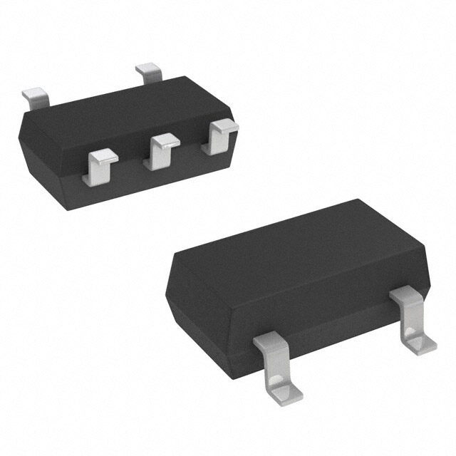
| 供应商器件封装 | SC-70-5 |
| 其它名称 | 296-24451-2 |
| 包装 | 带卷 (TR) |
| 单位重量 | 2.500 mg |
| 商标 | Texas Instruments |
| 回动电压—最大值 | 1.3 V at 80 mA |
| 安装类型 | 表面贴装 |
| 安装风格 | SMD/SMT |
| 封装 | Reel |
| 封装/外壳 | 6-TSSOP(5 引线),SC-88A,SOT-353 |
| 封装/箱体 | SC-70-5 |
| 工作温度 | -40°C ~ 125°C |
| 工厂包装数量 | 250 |
| 最大功率耗散 | 0.32 W |
| 最大工作温度 | + 125 C |
| 最大输入电压 | 10 V |
| 最小工作温度 | - 40 C |
| 最小输入电压 | + 2.5 V |
| 标准包装 | 250 |
| 电压-跌落(典型值) | 0.67V @ 80mA |
| 电压-输入 | 最高 10V |
| 电压-输出 | 3.3V |
| 电流-输出 | 80mA |
| 电流-限制(最小值) | 100mA |
| 稳压器拓扑 | 正,固定式 |
| 稳压器数 | 1 |
| 系列 | TPS71433 |
| 线路调整率 | 5 mV |
| 负载调节 | 30 mV |
| 输入偏压电流—最大 | 0.0032 mA |
| 输出电压 | 3.3 V |
| 输出电流 | 1.1 A |
| 输出端数量 | 1 Output |
| 输出类型 | Fixed |


- 商务部:美国ITC正式对集成电路等产品启动337调查
- 曝三星4nm工艺存在良率问题 高通将骁龙8 Gen1或转产台积电
- 太阳诱电将投资9.5亿元在常州建新厂生产MLCC 预计2023年完工
- 英特尔发布欧洲新工厂建设计划 深化IDM 2.0 战略
- 台积电先进制程称霸业界 有大客户加持明年业绩稳了
- 达到5530亿美元!SIA预计今年全球半导体销售额将创下新高
- 英特尔拟将自动驾驶子公司Mobileye上市 估值或超500亿美元
- 三星加码芯片和SET,合并消费电子和移动部门,撤换高东真等 CEO
- 三星电子宣布重大人事变动 还合并消费电子和移动部门
- 海关总署:前11个月进口集成电路产品价值2.52万亿元 增长14.8%


PDF Datasheet 数据手册内容提取
TPS714xx www.ti.com SBVS116C–DECEMBER2008–REVISEDMARCH2011 80mA, 10V, 3.2μA Quiescent Current LOW-DROPOUT LINEAR REGULATOR in SC70 or SON 2x2 FEATURES DESCRIPTION 1 • WideInputVoltageRange:2.5Vto10V The TPS714xx low-dropout (LDO) voltage regulators 2 offer the benefits of wide input voltage range, • LowQuiescentCurrent:3.2μAat80mA low-dropout voltage, low-power operation, and • StablewithanyCapacitor> 0.47μF miniaturized packaging. These devices, which • OutputCurrent:80mA operate over an input range of 2.5V to 10V, are stable with any capacitor ≥ 0.47μF. The 2.5V to 10V • DropoutVoltage:415mVat50mALoad input voltage range, combined with 3.2μA quiescent • AvailableinFixed3.3VorAdjustable(1.2Vto current, makes this device particularly well-suited for 8.8V)Versions two-cell alkaline, and two-cell lithium, and other low • CurrentLimit quiescent current sensitive battery applications. The low dropout voltage and low quiescent current allow • SC70-5and2mmx2mmSON-6Packages operation at extremely low power levels. Therefore, • SpecifiedJunctionTemperatureRange: the devices are ideal for power battery management –40°Cto+125°C ICs. Specifically, because the device is enabled as • ForMSP430-SpecificOutputVoltages,seethe soon as the applied voltage reaches the minimum input voltage, the output is quickly available to power TPS715xx continuously-operating,battery-chargingICs. APPLICATIONS ThetypicalPNPpasstransistorhasbeenreplacedby • Ultralow-PowerMicrocontrollers a PMOS pass element. Because the PMOS pass element behaves as a low-value resistor, the low • Industrial/AutomotiveApplications dropout voltage (typically 415mV at 50mA of load • PDAs current) is directly proportional to the load current. • Portable,Battery-PoweredEquipment The quiescent current (3.2μA, typical) is stable over the entire range of the output load current (0mA to 80mA). The TPS714xx is available in a 2mm x 2mm SON-6 package ideal for high power dissipation, or an SC70-5 package ideal for handheld and ultra-portable applications. DRV PACKAGE DCK PACKAGE TPS71433 2mm x 2mm SON SC70-5 IN OUT MSP430 (TOP VIEW) (TOP VIEW) GND IN 1 6 OUT FB/NC 1 5 OUT 9V D NC 2 N 5 NC GND 2 G GND 3 4 FB/NC NC 3 4 IN 1 Pleasebeawarethatanimportantnoticeconcerningavailability,standardwarranty,anduseincriticalapplicationsofTexas Instrumentssemiconductorproductsanddisclaimerstheretoappearsattheendofthisdatasheet. Alltrademarksarethepropertyoftheirrespectiveowners. 2 PRODUCTIONDATAinformationiscurrentasofpublicationdate. Copyright©2008–2011,TexasInstrumentsIncorporated Products conform to specifications per the terms of the Texas Instruments standard warranty. Production processing does not necessarilyincludetestingofallparameters.
TPS714xx SBVS116C–DECEMBER2008–REVISEDMARCH2011 www.ti.com This integrated circuit can be damaged by ESD. Texas Instruments recommends that all integrated circuits be handled with appropriateprecautions.Failuretoobserveproperhandlingandinstallationprocedurescancausedamage. ESDdamagecanrangefromsubtleperformancedegradationtocompletedevicefailure.Precisionintegratedcircuitsmaybemore susceptibletodamagebecauseverysmallparametricchangescouldcausethedevicenottomeetitspublishedspecifications. AVAILABLEOPTIONS(1) PRODUCT V (2) OUT XXisnominaloutputvoltage(forexample33=3.3V,01=Adjustable) TPS714xxyyyz YYYisPackageDesignator ZisPackageQuantity (1) ForthemostcurrentpackageandorderinginformationseethePackageOptionAddendumattheendofthisdocument,orseetheTI websiteatwww.ti.com. (2) Customoutputvoltagesareavailableonaquick-turnbasisforprototyping.Productionquantitiesareavailable;minimumpackageorder quantitiesapply.Contactfactoryfordetailsandavailability. ABSOLUTE MAXIMUM RATINGS Overoperatingtemperaturerange,unlessotherwisenoted.(1) PARAMETER TPS714xx UNIT V range –0.3to+24 V IN V range -0.3to+9.9 V OUT V -0.3to+4 V FBrange Peakoutputcurrent Internallylimited Continuoustotalpowerdissipation SeePowerDissipationRatingtable Junctiontemperaturerange,T –40to+125 °C J Storagetemperaturerange –65to+150 °C Humanbodymodel(HBM) 2 kV ESDrating Chargeddevicemodel(CDM) 500 V (1) StressesbeyondthoselistedunderAbsoluteMaximumRatingsmaycausepermanentdamagetothedevice.Thesearestressratings only,andfunctionaloperationofthedeviceattheseoranyotherconditionsbeyondthoseindicatedisnotimplied.Exposureto absolute-maximum-ratedconditionsforextendedperiodsmayaffectdevicereliability. POWER DISSIPATION RATING TABLE DERATINGFACTOR T ≤25°CPOWER T =+70°CPOWER T =+85°CPOWER A A A BOARD PACKAGE R °C/W ABOVET =+25°C RATING RATING RATING θJA A High-K(1) DCK 315 3.18mW/°C 320mW 175mW 100mW High-K(1) DRV 65 15.4mW/°C 1.54W 850mW 0.62W (1) TheJEDECHigh-K(2s2p)boarddesignusedtoderivethisdatawasa3inch×3inch,multilayerboardwith1-ounceinternalpowerand groundplanesand2-ouncecoppertracesontopandbottomoftheboard. 2 SubmitDocumentationFeedback Copyright©2008–2011,TexasInstrumentsIncorporated
TPS714xx www.ti.com SBVS116C–DECEMBER2008–REVISEDMARCH2011 ELECTRICAL CHARACTERISTICS Overtheoperatingjunctiontemperaturerange(T =–40°Cto+125°C),V =V +1V,I =1mA,andC =1μF, J IN OUT(NOM) OUT OUT unlessotherwisenoted.TheadjustableversionistestedwithV =2.8V.TypicalvaluesareatT =+25°C. OUT J TPS714xx PARAMETER TESTCONDITIONS MIN TYP MAX UNIT I =10mA 2.5 10 Inputvoltagerange(1) V OUT V IN I =80mA 3 10 OUT Outputvoltagerange V V V 8.8 (TPS71401) OUT FB Internalreference V V 1.12 1.20 1.24 (TPS71401) FB TPS71433 Outputvoltageaccuracy(1) overV ,I , 4.3V<V <10V,1mA≤I ≤80mA 3.135 3.3 3.465 V IN OUT IN OUT andTemp Outputvoltage lineregulation(1) ΔVOUT/ΔVIN VOUT+1V<VIN≤10V 5 mV Loadregulation ΔV /ΔI I =1mAto80mA 30 mV OUT OUT OUT Feedbackpinbiascurrent I I =0mA,V =3Vto10V,V =1.2V, 2 nA FBBIAS OUT IN OUT Dropoutvoltage V I =80mA,V =V –0.1V 670 1300 mV DO OUT IN OUT(NOM) Outputcurrentlimit I V =0V 100 1100 mA CL OUT T =–40°Cto+85°C,1mA≤I ≤80mA 3.2 4.2 J OUT Groundpincurrent I 1mA≤I ≤80mA 3.2 5.8 μA GND OUT V =10V,1mA≤I ≤80mA 7.4 IN OUT Power-supplyripple PSRR f=100kHz,C =10μF 60 dB rejection OUT BW=200Hzto100kHz, Outputnoisevoltage V 575 μVrms IN C =10μF,I =50mA OUT OUT (1) MinimumV =V +V ,orthevalueshownforInputvoltage,whicheverisgreater. IN OUT DO PIN CONFIGURATION DRVPACKAGE DCKPACKAGE SON-6 SC70-5 (TOPVIEW) (TOPVIEW) IN 1 6 OUT FB/NC 1 5 OUT D NC 2 N 5 NC G GND 2 GND 3 4 FB/NC NC 3 4 IN Table1.PinDescriptions TPS714xx DCK DRV NAME FIXED ADJ. FIXED ADJ. DESCRIPTION FB/NC - 1 - 4 Adjustableversiononly.Thispinisusedtosettheoutputvoltage. GND 2 2 3,Pad 3,Pad Ground Noconnection.Maybeleftopenortiedtogroundforimprovedthermal NC 1,3 3 2,4,5 2,5 performance. IN 4 4 1 1 Unregulatedinputvoltage. Regulatedoutputvoltage.Anyoutputcapacitor≥0.47μFcanbeusedfor OUT 5 5 6 6 stability. Copyright©2008–2011,TexasInstrumentsIncorporated SubmitDocumentationFeedback 3
TPS714xx SBVS116C–DECEMBER2008–REVISEDMARCH2011 www.ti.com FUNCTIONAL BLOCK DIAGRAMS V V IN OUT Current Sense I LIM R1 GND FB R2 V = 1.205V Bandgap REF Reference Figure1. AdjustableVoltageVersion V V IN OUT Current Sense I LIM R1 GND R2 840kW V = 1.205V Bandgap REF Reference Figure2. FixedVoltageVersion 4 SubmitDocumentationFeedback Copyright©2008–2011,TexasInstrumentsIncorporated
TPS714xx www.ti.com SBVS116C–DECEMBER2008–REVISEDMARCH2011 TYPICAL CHARACTERISTICS AtT =+25°C,unlessotherwisenoted. A TPS71433 TPS71433 TPS71433 OUTPUTVOLTAGE OUTPUTVOLTAGE QUIESCENTCURRENT vs vs vs OUTPUTCURRENT JUNCTIONTEMPERATURE JUNCTIONTEMPERATURE 3.465 3.465 4.5 3.432 VIN= 4.3V 3.432 VIN=4.3V VVIONU=T4=.33V.3V --VOutput VoltageVOUT 3333333.......333322296306309630741 --VDropout VoltagemVDO 3333333.......333322296306309630741 IOUTIO=U T80=m 1A0mA Ground -Current-AmGND 334...050 IOUT= 1mF 3.168 3.168 I 2.5 3.135 3.135 0 10 20 30 40 50 60 70 80 -40-25-10 5 20 35 50 65 80 95110125 2.0 IOUT-Output Current-mA TJ-Junction Temperature-°C -40-25-10 5 20 35 50 65 80 95110 125 TJ-Junction Temperature-°C Figure3. Figure4. Figure5. TPS71433 OUTPUTSPECTRALNOISE TPS71433 TPS71433 DENSITY OUTPUTIMPEDANCE DROPOUTVOLTAGE vs vs vs FREQUENCY FREQUENCY OUTPUTCURRENT 8 18 1000 mÖ-Output SV/Hpectral Noizse Density 1234567 IOIOUUTT==15m0AmA VVCIOONUU=TT4==. 331Vm.3FV --WZOutput ImpedanceO1111420680246 VVCTIOJIOONU=UUTI=TOT+=U4==2T.15 331m°=Vm.C3AF5V0mA --VDromVpoutVoltageDO 9876543210000000000000000000 VIN= 4.3VTJ= +2T5J°=CT-J4=0 °+C125°C 0 0 10 20 30 40 50 60 70 80 100 1k 10k 100k 10 100 1k 10k 100k 1M 10M I -OutputCurrent-mA f-Frequency-Hz f-Frequency-Hz OUT Figure6. Figure7. Figure8. Copyright©2008–2011,TexasInstrumentsIncorporated SubmitDocumentationFeedback 5
TPS714xx SBVS116C–DECEMBER2008–REVISEDMARCH2011 www.ti.com TYPICAL CHARACTERISTICS (continued) AtT =+25°C,unlessotherwisenoted. A TPS71433 TPS71433 TPS71433 POWER-SUPPLYRIPPLE DROPOUTVOLTAGE V REJECTION OUT vs vs vs JUNCTIONTEMPERATURE CURRENTLIMIT FREQUENCY 1000 3.5 100 900 VIN= 4.3V 3.0 VVIN== 43..33VV -ndB 90 VVIONU=T4=.33V.3V --VDropout VoltagemVDO 876543210000000000000000 IOUT= 80mA IOUT= 10mA --ltVOutputVoageVOUT 22110.....50505 OUT -Power Supply Ripple Rejectio 48572360000000 CTJO=UT+2=5 1°0CmIOFUT=1mAIOUT=50mA R 0 0 SR 10 -40-25-10 5 20 35 50 65 80 95110125 0 100 200 300 400 500 P 0 TJ-Junction Temperature-°C IOUT-CurrentLimit-mA 10 100 1k 10k 100k 1M 10M f-Frequency-Hz Figure9. Figure10. Figure11. TPS71433 TPS71433 TPS71433 POWER-UP/POWER-DOWN LINETRANSIENTRESPONSE LOADTRANSIENTRESPONSE --VOutput VoltageVOUT--VInput VoltageVIN 87654321 VVRCINOLOUU=TT 6==6 W31.03VmVOFUT -put VoltageV --VOutput VoltagemVOUT1-50550.0003 VICOOOUUUTTT===5 310.0m3mVAF -OutputCurmArent --ltVOutputVoagemVOUT -122500000000 VVCIOONUU=TT ==4 .313.0V3mVF n 0 0 2 4 6 8 10 12 14 16 18 20 -VIIN 4.30 50 100150200250300350400450 500 -IOUT 0-0.5 0 0.5 1.0t1-.5Tim2.e0-2m.5s3.03.5 4.0 4.5 t-Time-ms t-Time-ms Figure12. Figure13. Figure14. 6 SubmitDocumentationFeedback Copyright©2008–2011,TexasInstrumentsIncorporated
TPS714xx www.ti.com SBVS116C–DECEMBER2008–REVISEDMARCH2011 APPLICATION INFORMATION The TPS714xx family of LDO regulators has been optimized for ultralow power applications such as the MSP430 microcontroller. Its ultralow supply current maximizes efficiency at light loads, and its high input voltage range makesitsuitableforsuppliessuchasunconditionedsolarpanels. TPS71433 VIN IN OUT VOUT 0.1CmF1 GND 0.47mF Figure15. TypicalApplicationCircuit(FixedVoltageVersion) External Capacitor Requirements Although not required, a 0.047μF or larger input bypass capacitor, connected between IN and GND and located close to the device, is recommended to improve transient response and noise rejection of the power supply as a whole.Ahigher-valueinputcapacitormaybenecessaryiflarge,fast-rise-timeloadtransientsareanticipatedand ifthedeviceislocatedseveralinchesfromthepowersource. The TPS714xx requires an output capacitor connected between OUT and GND to stabilize the internal control loop. Any capacitor (including ceramic and tantalum) that is greater than or equal to 0.47μF properly stabilizes thisloop. Power Dissipation and Junction Temperature To ensure reliable operation, worst-case junction temperature should not exceed +125°C. This restriction limits the power dissipation that the regulator can manage in any given application. To ensure the junction temperature is within acceptable limits, calculate the maximum allowable dissipation, P , and the actual dissipation, P , D(MAX) D whichmustbelessthanorequaltoP . D(max) Themaximum-power-dissipationlimitisdeterminedusingEquation1: T max(cid:1)T P (cid:2) J A D(max) R (cid:1)JA Where: • Tmaxisthemaximumallowablejunctiontemperature. J • R isthethermalresistancejunction-to-ambientforthepackage(seethePowerDissipationRatingtable). θJA • T istheambienttemperature. (1) A TheregulatordissipationiscalculatedusingEquation2: PD(cid:3)(cid:4)VIN(cid:2)VOUT(cid:5)(cid:1)IOUT (2) Powerdissipationresultingfromquiescentcurrentisnegligible. Regulator Protection The TPS714xx PMOS-pass transistor has a built-in back diode that conducts reverse current when the input voltage drops below the output voltage (for example, during power-down). Current is conducted from the output to the input and is not internally limited. If extended reverse voltage operation is anticipated, external limiting mightbeappropriate. The TPS714xx features internal current limiting. During normal operation, the TPS714xx limits output current to approximately 500mA. When current limiting engages, the output voltage scales back linearly until the over-current condition ends. There is no internal thermal shutdown circuit in this device; therefore, care must be taken not to exceed the power dissipation ratings of the package during a fault condition. This device does not haveundervoltagelockout;therefore,thisconstraintshouldbetakenintoconsiderationforspecificapplications. Copyright©2008–2011,TexasInstrumentsIncorporated SubmitDocumentationFeedback 7
TPS714xx SBVS116C–DECEMBER2008–REVISEDMARCH2011 www.ti.com Programming the TPS71401 Adjustable LDO Regulator The output voltage of the TPS71401 adjustable regulator is programmed using an external resistor divider as showninFigure16.TheoutputvoltageiscalculatedusingEquation3: (cid:4) R1(cid:5) VOUT(cid:3)VREF(cid:1) 1(cid:2)R2 (3) where: V =1.20Vtyp(theinternalreferencevoltage) REF Resistors R1 and R2 should be chosen for approximately a 1.5μA divider current. Lower value resistors can be used for improved noise performance, but the solution consumes more power. Higher resistor values should be avoided because leakage current out of the FB pin across R1/R2 creates an offset voltage that artificially increases the feedback voltage and thus erroneously decreases V . The recommended design procedure is to OUT chooseR2=1MΩ tosetthedividercurrentat1.5μA,andthencalculateR1usingEquation4: (cid:4)VOUT (cid:5) R1(cid:3) (cid:2)1 (cid:1)R2 V REF (4) TPS71401 OUTPUT VOLTAGE VIN IN PROGRAMMING GUIDE 0.1mF OUTPUT VOLTAGE R1 R2 OUT VOUT 1.8V 392MW 806kW R1 2.8V 1.07MW 806kW FB 0.47mF 5.0V 2.55MW 806kW GND R2 Figure16. TPS71401AdjustableLDORegulatorProgramming 8 SubmitDocumentationFeedback Copyright©2008–2011,TexasInstrumentsIncorporated
TPS714xx www.ti.com SBVS116C–DECEMBER2008–REVISEDMARCH2011 REVISION HISTORY NOTE:Pagenumbersforpreviousrevisionsmaydifferfrompagenumbersinthecurrentversion. ChangesfromRevisionB(December,2009)toRevisionC Page • ChangedGroundpincurrentmaximumspecifications ......................................................................................................... 3 ChangesfromRevisionA(April,2009)toRevisionB Page • Changedbatterytypeshownintypicalcircuitillustration ..................................................................................................... 1 • ChangedV rangeabsolutemaximumratingfrom+11.5Vto+24V ................................................................................... 2 IN Copyright©2008–2011,TexasInstrumentsIncorporated SubmitDocumentationFeedback 9
PACKAGE OPTION ADDENDUM www.ti.com 6-Feb-2020 PACKAGING INFORMATION Orderable Device Status Package Type Package Pins Package Eco Plan Lead/Ball Finish MSL Peak Temp Op Temp (°C) Device Marking Samples (1) Drawing Qty (2) (6) (3) (4/5) TPS71401DCKR ACTIVE SC70 DCK 5 3000 Green (RoHS NIPDAUAG Level-1-260C-UNLIM -40 to 125 CVG & no Sb/Br) TPS71401DCKT ACTIVE SC70 DCK 5 250 Green (RoHS NIPDAUAG Level-1-260C-UNLIM -40 to 125 CVG & no Sb/Br) TPS71401DRVR ACTIVE WSON DRV 6 3000 Green (RoHS NIPDAU Level-1-260C-UNLIM -40 to 125 CVG & no Sb/Br) TPS71401DRVT ACTIVE WSON DRV 6 250 Green (RoHS NIPDAU Level-1-260C-UNLIM -40 to 125 CVG & no Sb/Br) TPS71433DCKR ACTIVE SC70 DCK 5 3000 Green (RoHS NIPDAUAG Level-1-260C-UNLIM -40 to 125 CVH & no Sb/Br) TPS71433DCKT ACTIVE SC70 DCK 5 250 Green (RoHS NIPDAUAG Level-1-260C-UNLIM -40 to 125 CVH & no Sb/Br) TPS71433DRVR ACTIVE WSON DRV 6 3000 Green (RoHS NIPDAU Level-1-260C-UNLIM -40 to 125 CVH & no Sb/Br) TPS71433DRVT ACTIVE WSON DRV 6 250 Green (RoHS NIPDAU Level-1-260C-UNLIM -40 to 125 CVH & no Sb/Br) (1) The marketing status values are defined as follows: ACTIVE: Product device recommended for new designs. LIFEBUY: TI has announced that the device will be discontinued, and a lifetime-buy period is in effect. NRND: Not recommended for new designs. Device is in production to support existing customers, but TI does not recommend using this part in a new design. PREVIEW: Device has been announced but is not in production. Samples may or may not be available. OBSOLETE: TI has discontinued the production of the device. (2) RoHS: TI defines "RoHS" to mean semiconductor products that are compliant with the current EU RoHS requirements for all 10 RoHS substances, including the requirement that RoHS substance do not exceed 0.1% by weight in homogeneous materials. Where designed to be soldered at high temperatures, "RoHS" products are suitable for use in specified lead-free processes. TI may reference these types of products as "Pb-Free". RoHS Exempt: TI defines "RoHS Exempt" to mean products that contain lead but are compliant with EU RoHS pursuant to a specific EU RoHS exemption. Green: TI defines "Green" to mean the content of Chlorine (Cl) and Bromine (Br) based flame retardants meet JS709B low halogen requirements of <=1000ppm threshold. Antimony trioxide based flame retardants must also meet the <=1000ppm threshold requirement. (3) MSL, Peak Temp. - The Moisture Sensitivity Level rating according to the JEDEC industry standard classifications, and peak solder temperature. (4) There may be additional marking, which relates to the logo, the lot trace code information, or the environmental category on the device. Addendum-Page 1
PACKAGE OPTION ADDENDUM www.ti.com 6-Feb-2020 (5) Multiple Device Markings will be inside parentheses. Only one Device Marking contained in parentheses and separated by a "~" will appear on a device. If a line is indented then it is a continuation of the previous line and the two combined represent the entire Device Marking for that device. (6) Lead/Ball Finish - Orderable Devices may have multiple material finish options. Finish options are separated by a vertical ruled line. Lead/Ball Finish values may wrap to two lines if the finish value exceeds the maximum column width. Important Information and Disclaimer:The information provided on this page represents TI's knowledge and belief as of the date that it is provided. TI bases its knowledge and belief on information provided by third parties, and makes no representation or warranty as to the accuracy of such information. Efforts are underway to better integrate information from third parties. TI has taken and continues to take reasonable steps to provide representative and accurate information but may not have conducted destructive testing or chemical analysis on incoming materials and chemicals. TI and TI suppliers consider certain information to be proprietary, and thus CAS numbers and other limited information may not be available for release. In no event shall TI's liability arising out of such information exceed the total purchase price of the TI part(s) at issue in this document sold by TI to Customer on an annual basis. Addendum-Page 2
PACKAGE MATERIALS INFORMATION www.ti.com 15-Feb-2018 TAPE AND REEL INFORMATION *Alldimensionsarenominal Device Package Package Pins SPQ Reel Reel A0 B0 K0 P1 W Pin1 Type Drawing Diameter Width (mm) (mm) (mm) (mm) (mm) Quadrant (mm) W1(mm) TPS71401DCKR SC70 DCK 5 3000 180.0 8.4 2.41 2.41 1.2 4.0 8.0 Q3 TPS71401DCKT SC70 DCK 5 250 180.0 8.4 2.41 2.41 1.2 4.0 8.0 Q3 TPS71401DRVR WSON DRV 6 3000 179.0 8.4 2.2 2.2 1.2 4.0 8.0 Q2 TPS71401DRVT WSON DRV 6 250 179.0 8.4 2.2 2.2 1.2 4.0 8.0 Q2 TPS71433DCKR SC70 DCK 5 3000 180.0 8.4 2.41 2.41 1.2 4.0 8.0 Q3 TPS71433DCKT SC70 DCK 5 250 180.0 8.4 2.41 2.41 1.2 4.0 8.0 Q3 TPS71433DRVR WSON DRV 6 3000 179.0 8.4 2.2 2.2 1.2 4.0 8.0 Q2 TPS71433DRVT WSON DRV 6 250 179.0 8.4 2.2 2.2 1.2 4.0 8.0 Q2 PackMaterials-Page1
PACKAGE MATERIALS INFORMATION www.ti.com 15-Feb-2018 *Alldimensionsarenominal Device PackageType PackageDrawing Pins SPQ Length(mm) Width(mm) Height(mm) TPS71401DCKR SC70 DCK 5 3000 183.0 183.0 20.0 TPS71401DCKT SC70 DCK 5 250 183.0 183.0 20.0 TPS71401DRVR WSON DRV 6 3000 203.0 203.0 35.0 TPS71401DRVT WSON DRV 6 250 203.0 203.0 35.0 TPS71433DCKR SC70 DCK 5 3000 183.0 183.0 20.0 TPS71433DCKT SC70 DCK 5 250 183.0 183.0 20.0 TPS71433DRVR WSON DRV 6 3000 203.0 203.0 35.0 TPS71433DRVT WSON DRV 6 250 203.0 203.0 35.0 PackMaterials-Page2
None
None
GENERIC PACKAGE VIEW DRV 6 WSON - 0.8 mm max height PLASTIC SMALL OUTLINE - NO LEAD Images above are just a representation of the package family, actual package may vary. Refer to the product data sheet for package details. 4206925/F
PACKAGE OUTLINE DRV0006A WSON - 0.8 mm max height SCALE 5.500 PLASTIC SMALL OUTLINE - NO LEAD B 2.1 A 1.9 PIN 1 INDEX AREA 2.1 1.9 0.8 C 0.7 SEATING PLANE 0.08 C (0.2) TYP 1 0.1 0.05 EXPOSED 0.00 THERMAL PAD 3 4 2X 7 1.3 1.6 0.1 6 1 4X 0.65 0.35 6X PIN 1 ID 0.3 0.25 6X (OPTIONAL) 0.2 0.1 C A B 0.05 C 4222173/B 04/2018 NOTES: 1. All linear dimensions are in millimeters. Any dimensions in parenthesis are for reference only. Dimensioning and tolerancing per ASME Y14.5M. 2. This drawing is subject to change without notice. 3. The package thermal pad must be soldered to the printed circuit board for thermal and mechanical performance. www.ti.com
EXAMPLE BOARD LAYOUT DRV0006A WSON - 0.8 mm max height PLASTIC SMALL OUTLINE - NO LEAD 6X (0.45) (1) 1 7 6X (0.3) 6 SYMM (1.6) (1.1) 4X (0.65) 4 3 (R0.05) TYP SYMM ( 0.2) VIA (1.95) TYP LAND PATTERN EXAMPLE SCALE:25X 0.07 MAX 0.07 MIN ALL AROUND ALL AROUND SOLDER MASK METAL METAL UNDER SOLDER MASK OPENING SOLDER MASK OPENING NON SOLDER MASK DEFINED SOLDER MASK (PREFERRED) DEFINED SOLDER MASK DETAILS 4222173/B 04/2018 NOTES: (continued) 4. This package is designed to be soldered to a thermal pad on the board. For more information, see Texas Instruments literature number SLUA271 (www.ti.com/lit/slua271). 5. Vias are optional depending on application, refer to device data sheet. If some or all are implemented, recommended via locations are shown. www.ti.com
EXAMPLE STENCIL DESIGN DRV0006A WSON - 0.8 mm max height PLASTIC SMALL OUTLINE - NO LEAD SYMM 6X (0.45) METAL 1 7 6X (0.3) 6 (0.45) SYMM 4X (0.65) (0.7) 4 3 (R0.05) TYP (1) (1.95) SOLDER PASTE EXAMPLE BASED ON 0.125 mm THICK STENCIL EXPOSED PAD #7 88% PRINTED SOLDER COVERAGE BY AREA UNDER PACKAGE SCALE:30X 4222173/B 04/2018 NOTES: (continued) 6. Laser cutting apertures with trapezoidal walls and rounded corners may offer better paste release. IPC-7525 may have alternate design recommendations. www.ti.com
PACKAGE OUTLINE DRV0006D WSON - 0.8 mm max height SCALE 5.500 PLASTIC SMALL OUTLINE - NO LEAD B 2.1 A 1.9 PIN 1 INDEX AREA 2.1 1.9 0.8 C 0.7 SEATING PLANE 0.08 C (0.2) TYP 1 0.1 0.05 EXPOSED 0.00 THERMAL PAD 3 4 2X 7 1.3 1.6 0.1 6 1 4X 0.65 0.35 6X PIN 1 ID 0.3 0.25 6X (OPTIONAL) 0.2 0.1 C A B 0.05 C 4225563/A 12/2019 NOTES: 1. All linear dimensions are in millimeters. Any dimensions in parenthesis are for reference only. Dimensioning and tolerancing per ASME Y14.5M. 2. This drawing is subject to change without notice. 3. The package thermal pad must be soldered to the printed circuit board for thermal and mechanical performance. www.ti.com
EXAMPLE BOARD LAYOUT DRV0006D WSON - 0.8 mm max height PLASTIC SMALL OUTLINE - NO LEAD 6X (0.45) (1) 1 7 6X (0.3) 6 SYMM (1.6) (1.1) 4X (0.65) 4 3 (R0.05) TYP SYMM ( 0.2) VIA (1.95) TYP LAND PATTERN EXAMPLE EXPOSED METAL SHOWN SCALE:25X 0.07 MAX 0.07 MIN ALL AROUND ALL AROUND EXPOSED EXPOSED METAL METAL SOLDER MASK METAL METAL UNDER SOLDER MASK OPENING SOLDER MASK OPENING NON SOLDER MASK DEFINED SOLDER MASK (PREFERRED) DEFINED SOLDER MASK DETAILS 4225563/A 12/2019 NOTES: (continued) 4. This package is designed to be soldered to a thermal pad on the board. For more information, see Texas Instruments literature number SLUA271 (www.ti.com/lit/slua271). 5. Vias are optional depending on application, refer to device data sheet. If some or all are implemented, recommended via locations are shown. www.ti.com
EXAMPLE STENCIL DESIGN DRV0006D WSON - 0.8 mm max height PLASTIC SMALL OUTLINE - NO LEAD SYMM 6X (0.45) METAL 1 7 6X (0.3) 6 (0.45) SYMM 4X (0.65) (0.7) 4 3 (R0.05) TYP (1) (1.95) SOLDER PASTE EXAMPLE BASED ON 0.125 mm THICK STENCIL EXPOSED PAD #7 88% PRINTED SOLDER COVERAGE BY AREA UNDER PACKAGE SCALE:30X 4225563/A 12/2019 NOTES: (continued) 6. Laser cutting apertures with trapezoidal walls and rounded corners may offer better paste release. IPC-7525 may have alternate design recommendations. www.ti.com
IMPORTANTNOTICEANDDISCLAIMER TI PROVIDES TECHNICAL AND RELIABILITY DATA (INCLUDING DATASHEETS), DESIGN RESOURCES (INCLUDING REFERENCE DESIGNS), APPLICATION OR OTHER DESIGN ADVICE, WEB TOOLS, SAFETY INFORMATION, AND OTHER RESOURCES “AS IS” AND WITH ALL FAULTS, AND DISCLAIMS ALL WARRANTIES, EXPRESS AND IMPLIED, INCLUDING WITHOUT LIMITATION ANY IMPLIED WARRANTIES OF MERCHANTABILITY, FITNESS FOR A PARTICULAR PURPOSE OR NON-INFRINGEMENT OF THIRD PARTY INTELLECTUAL PROPERTY RIGHTS. These resources are intended for skilled developers designing with TI products. You are solely responsible for (1) selecting the appropriate TI products for your application, (2) designing, validating and testing your application, and (3) ensuring your application meets applicable standards, and any other safety, security, or other requirements. These resources are subject to change without notice. TI grants you permission to use these resources only for development of an application that uses the TI products described in the resource. Other reproduction and display of these resources is prohibited. No license is granted to any other TI intellectual property right or to any third party intellectual property right. TI disclaims responsibility for, and you will fully indemnify TI and its representatives against, any claims, damages, costs, losses, and liabilities arising out of your use of these resources. TI’s products are provided subject to TI’s Terms of Sale (www.ti.com/legal/termsofsale.html) or other applicable terms available either on ti.com or provided in conjunction with such TI products. TI’s provision of these resources does not expand or otherwise alter TI’s applicable warranties or warranty disclaimers for TI products. Mailing Address: Texas Instruments, Post Office Box 655303, Dallas, Texas 75265 Copyright © 2020, Texas Instruments Incorporated