ICGOO在线商城 > 集成电路(IC) > PMIC - 稳压器 - 线性 > TPS70950DBVR
 Datasheet下载
- 型号: TPS70950DBVR
- 制造商: Texas Instruments
- 库位|库存: xxxx|xxxx
- 要求:
| 数量阶梯 | 香港交货 | 国内含税 |
| +xxxx | $xxxx | ¥xxxx |
查看当月历史价格
查看今年历史价格
TPS70950DBVR产品简介:
ICGOO电子元器件商城为您提供TPS70950DBVR由Texas Instruments设计生产,在icgoo商城现货销售,并且可以通过原厂、代理商等渠道进行代购。 TPS70950DBVR价格参考。Texas InstrumentsTPS70950DBVR封装/规格:PMIC - 稳压器 - 线性, Linear Voltage Regulator IC 1 Output 150mA SOT-23-5。您可以下载TPS70950DBVR参考资料、Datasheet数据手册功能说明书,资料中有TPS70950DBVR 详细功能的应用电路图电压和使用方法及教程。
TPS70950DBVR是Texas Instruments(德州仪器)推出的一款低压差线性稳压器(LDO),属于PMIC - 稳压器 - 线性产品类别。该器件输出电压固定为5.0V,最大输出电流可达30mA,具有超低静态电流(典型值为1.8µA),并支持宽输入电压范围(2.7V至15V),具备良好的线路和负载调节能力。

其主要应用场景包括:

1. 电池供电设备:由于其超低静态电流特性,非常适合用于对功耗敏感的便携式设备,如无线传感器、可穿戴设备和物联网(IoT)终端,有助于延长电池寿命。

2. 工业控制系统:在PLC模块、传感器信号调理电路和工业自动化设备中,TPS70950DBVR可为微控制器、ADC或其他模拟电路提供稳定可靠的5V电源。

3. 汽车电子:适用于车载信息娱乐系统、远程无钥匙进入系统等需要宽输入电压范围以应对冷启动或负载突降的应用场景。

4. 消费类电子产品:可用于小型家电、遥控器、智能仪表等设备中的电源管理单元,提供干净稳定的电压输出。

5. 电源噪声敏感系统:该LDO具有高电源抑制比(PSRR),能有效抑制输入端噪声,适合为精密模拟电路或RF模块供电。

综上所述,TPS70950DBVR凭借其低功耗、高稳定性与宽输入电压优势,广泛应用于对效率和可靠性要求较高的嵌入式系统和低功耗设计中。
| 参数 | 数值 |
| 产品目录 | 集成电路 (IC)半导体 |
| 描述 | IC REG LDO 5V 0.15A SOT23-5低压差稳压器 150mA 30V Ultra-Lo IQ Wd Input LDO Reg |
| 产品分类 | |
| 品牌 | Texas Instruments |
| 产品手册 | |
| 产品图片 |
|
| rohs | 符合RoHS无铅 / 符合限制有害物质指令(RoHS)规范要求 |
| 产品系列 | 电源管理 IC,低压差稳压器,Texas Instruments TPS70950DBVR- |
| 数据手册 | |
| 产品型号 | TPS70950DBVR |
| PSRR/纹波抑制—典型值 | 80 dB |
| 产品 | Voltage Regulators |
| 产品种类 | 低压差稳压器 |
| 供应商器件封装 | SOT-23-5 |
| 其它名称 | 296-35484-1 |
| 包装 | 剪切带 (CT) |
| 商标 | Texas Instruments |
| 安装类型 | 表面贴装 |
| 安装风格 | SMD/SMT |
| 封装 | Reel |
| 封装/外壳 | SC-74A,SOT-753 |
| 封装/箱体 | SOT-23-5 |
| 工作温度 | -40°C ~ 85°C |
| 工厂包装数量 | 3000 |
| 最大功率耗散 | - |
| 最大工作温度 | + 85 C |
| 最大输入电压 | 30 V |
| 最小工作温度 | - 40 C |
| 最小输入电压 | 2.7 V |
| 极性 | Positive |
| 标准包装 | 1 |
| 电压-跌落(典型值) | 0.69V @ 150mA |
| 电压-输入 | 最高 30V |
| 电压-输出 | 5V |
| 电流-输出 | 150mA |
| 电流-限制(最小值) | 200mA |
| 稳压器拓扑 | 正,固定式 |
| 稳压器数 | 1 |
| 类型 | Voltage Linear Regulator with Enable |
| 系列 | TPS70950 |
| 线路调整率 | 3 mV |
| 负载调节 | 20 mV |
| 输出电压 | 5 V |
| 输出电流 | 150 mA |
| 输出端数量 | 1 Output |
| 输出类型 | Fixed |


- 商务部:美国ITC正式对集成电路等产品启动337调查
- 曝三星4nm工艺存在良率问题 高通将骁龙8 Gen1或转产台积电
- 太阳诱电将投资9.5亿元在常州建新厂生产MLCC 预计2023年完工
- 英特尔发布欧洲新工厂建设计划 深化IDM 2.0 战略
- 台积电先进制程称霸业界 有大客户加持明年业绩稳了
- 达到5530亿美元!SIA预计今年全球半导体销售额将创下新高
- 英特尔拟将自动驾驶子公司Mobileye上市 估值或超500亿美元
- 三星加码芯片和SET,合并消费电子和移动部门,撤换高东真等 CEO
- 三星电子宣布重大人事变动 还合并消费电子和移动部门
- 海关总署:前11个月进口集成电路产品价值2.52万亿元 增长14.8%


PDF Datasheet 数据手册内容提取
Product Sample & Technical Tools & Support & Folder Buy Documents Software Community TPS709 SBVS186G–MARCH2012–REVISEDNOVEMBER2015 TPS709 150-mA, 30-V, 1-µA I Voltage Regulators with Enable Q 1 Features 3 Description • UltralowI :1μA The TPS709 series of linear regulators are ultralow, 1 Q quiescent current devices designed for power- • ReverseCurrentProtection sensitive applications. A precision band-gap and error • LowISHUTDOWN:150nA amplifier provides 2% accuracy over temperature. • InputVoltageRange:2.7Vto30V Quiescent current of only 1 µA makes these devices ideal solutions for battery-powered, always-on • Supports200-mAPeakOutput systems that require very little idle-state power • 2%AccuracyOverTemperature dissipation. These devices have thermal-shutdown, • AvailableinFixed-OutputVoltages: current-limit, and reverse-current protections for 1.2Vto6.5V addedsafety. • ThermalShutdownandOvercurrentProtection Shutdown mode is enabled by pulling the EN pin low. • Packages:SOT-23-5,WSON-6 The shutdown current in this mode goes down to 150 nA,typical. 2 Applications The TPS709 series is available in WSON-6 and • Zigbee™Networks SOT-23-5packages. • HomeAutomation DeviceInformation(1) • Metering PARTNUMBER PACKAGE BODYSIZE(NOM) • WeighingScales SOT-23(5) 2.90mm×1.60mm TPS709 • PortablePowerTools WSON(6) 2.00mm×2.00mm • RemoteControlDevices (1) Forallavailablepackages,seethepackageoptionaddendum • WirelessHandsets,SmartPhones,PDAs,WLAN, attheendofthedatasheet. andOtherPCAdd-OnCards • WhiteGoods TypicalApplicationCircuit GNDCurrentvsV andTemperature IN 2 VIN IN OUT VOUT 1mF 2.2mF 1.8 GND TPS709xx µA) nt ( 1.5 e EN NC urr C 1.2 n Pi d n 1 u o Gr 0.8 TA = −40°C TA = +25°C TPS70912 TA = +85°C 0.5 0 5 10 15 20 25 30 35 Input Voltage (V) G014 1 An IMPORTANT NOTICE at the end of this data sheet addresses availability, warranty, changes, use in safety-critical applications, intellectualpropertymattersandotherimportantdisclaimers.PRODUCTIONDATA.
TPS709 SBVS186G–MARCH2012–REVISEDNOVEMBER2015 www.ti.com Table of Contents 1 Features.................................................................. 1 8 ApplicationandImplementation........................ 15 2 Applications........................................................... 1 8.1 ApplicationInformation............................................15 3 Description............................................................. 1 8.2 TypicalApplication .................................................15 4 RevisionHistory..................................................... 2 9 PowerSupplyRecommendations...................... 16 5 PinConfigurationandFunctions......................... 4 9.1 PowerDissipation...................................................16 6 Specifications......................................................... 5 10 Layout................................................................... 17 6.1 AbsoluteMaximumRatings......................................5 10.1 LayoutGuidelines.................................................17 6.2 ESDRatings..............................................................5 10.2 LayoutExample....................................................17 6.3 RecommendedOperatingConditions.......................5 11 DeviceandDocumentationSupport................. 18 6.4 ThermalInformation..................................................5 11.1 DeviceSupport......................................................18 6.5 ElectricalCharacteristics...........................................6 11.2 DocumentationSupport........................................18 6.6 TypicalCharacteristics..............................................7 11.3 CommunityResources..........................................18 7 DetailedDescription............................................ 13 11.4 Trademarks...........................................................19 7.1 Overview.................................................................13 11.5 ElectrostaticDischargeCaution............................19 7.2 FunctionalBlockDiagram.......................................13 11.6 Glossary................................................................19 7.3 FeatureDescription.................................................13 12 Mechanical,Packaging,andOrderable Information........................................................... 19 7.4 DeviceFunctionalModes........................................14 4 Revision History NOTE:Pagenumbersforpreviousrevisionsmaydifferfrompagenumbersinthecurrentversion. ChangesfromRevisionF(December2014)toRevisionG Page • AddedDBVpackageforTPS709AtoPinConfigurationsandFunctionssection.................................................................. 4 • AddedDBVpackageforTPS709BtoPinConfigurationsandFunctionssection.................................................................. 4 • AddedTPS709AandTPS709BtoPinFunctionstable......................................................................................................... 4 • MovedoperatingjunctiontemperaturefromElectricalCharacteristicstoRecommendedOperatingConditions.................5 ChangesfromRevisionE(November2013)toRevisionF Page • Changedtitleformattomeetlatestdatasheetstandards...................................................................................................... 1 • AddedESDRatingtable,FeatureDescriptionsection,DeviceFunctionalModes,ApplicationandImplementation section,PowerSupplyRecommendationssection,Layoutsection,DeviceandDocumentationSupportsection,and Mechanical,Packaging,andOrderableInformationsection.................................................................................................. 1 • DeletedSOT-223-4packagefromdocument........................................................................................................................ 1 • DeletedLowDropoutFeaturesbullet .................................................................................................................................... 1 • ChangedPackagesFeaturebullet:deletedSOT-223-4andfootnote .................................................................................. 1 • DeletedSOT-223-4fromlastparagraphofDescriptionsection ........................................................................................... 1 • Deletedpinoutgraphicsfrompage1 .................................................................................................................................... 1 • DeletedDCYpackageandfootnotefromPinConfigurationssection................................................................................... 4 • ChangedPinFunctionstable:changedtitleanddeletedDCYpackage................................................................................ 4 • ChangedENpindescriptioninPinFunctionstable .............................................................................................................. 4 • Deletedtheword'range'fromthelast2rowsoftheAbsoluteMaximumRatingstable........................................................ 5 • DeletedDCYcolumnfromThermalInformationtable........................................................................................................... 5 • AddeddescriptiontexttotheenabledmodediscussionintheDeviceFunctionalModessection ..................................... 14 2 SubmitDocumentationFeedback Copyright©2012–2015,TexasInstrumentsIncorporated ProductFolderLinks:TPS709
TPS709 www.ti.com SBVS186G–MARCH2012–REVISEDNOVEMBER2015 ChangesfromRevisionD(October2013)toRevisionE Page • ChangedDRV(SON-6)packagestatusfromPreviewtoProductionData............................................................................ 1 • DeletedSON-6packagefromfootnote1inFeaturessection................................................................................................ 1 • DeletedDRVpackagefrompinoutdiagramnote................................................................................................................... 1 • DeletedDRVfrompinoutnoteinthePinConfigurationssection........................................................................................... 4 ChangesfromRevisionC(June2013)toRevisionD Page • ChangeddevicestatusfromProductionDatatoMixedStatus.............................................................................................. 1 • ChangedlastFeaturesbullet:addedfootnoteandchangeddeviceorder............................................................................. 1 • Addednotetopinoutdiagrams............................................................................................................................................... 1 • Addedproductpreviewfootnotetopinconfigurations........................................................................................................... 4 ChangesfromRevisionB(November2012)toRevisionC Page • AddedDCY(SOT-223)andDRV(SON)packagestodatasheet......................................................................................... 1 • ChangedI featurebulletvaluefrom1.35µAto1µA........................................................................................................... 1 Q • ChangedquiescentcurrentvalueinfirstparagraphofDescriptionsectionfrom1.35µAto1µA........................................ 1 • ChangedtextinsecondparagraphofDescriptionsectionfrom"leakage"to"shutdown.".................................................... 1 • Addedtypicalapplicationcircuit............................................................................................................................................. 1 • AddedDCYandDRVpackagestoPinConfigurationsection .............................................................................................. 4 • AddedDCYandDRVpackagestoPinDescriptionstable ................................................................................................... 4 • AddedDRVandDCYpackagestoThermalInformationtable.............................................................................................. 5 • ChangedgroundpincurrenttypicalvaluesforI =0-mAtestconditions........................................................................... 6 OUT ChangesfromRevisionA(October2012)toRevisionB Page • AddedPinConfigurationsection............................................................................................................................................ 4 • ChangedLineregulationandLoadregulationparametersinElectricalCharacteristicstable............................................... 6 • ChangedI parametertestconditionsinElectricalCharacteristicstable........................................................................... 6 GND • ChangedI parametertestconditionsinElectricalCharacteristicstable.................................................................. 6 SHUTDOWN • Changedfootnote4inElectricalCharacteristicstable........................................................................................................... 6 • ChangedsecondparagraphofDropoutVoltagesection..................................................................................................... 13 ChangesfromOriginal(March2012)toRevisionA Page • ChangeddevicestatusfromProductPreviewtoProductionData........................................................................................ 1 Copyright©2012–2015,TexasInstrumentsIncorporated SubmitDocumentationFeedback 3 ProductFolderLinks:TPS709
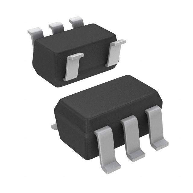
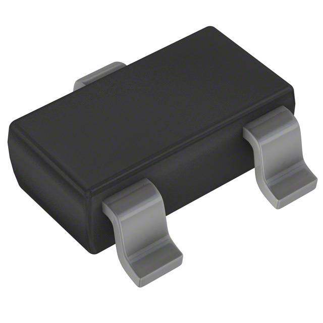
TPS709 SBVS186G–MARCH2012–REVISEDNOVEMBER2015 www.ti.com 5 Pin Configuration and Functions TPS709:DBVPackage 5-PinSOT-23 TPS709B:DBVPackage TopView 5-PinSOT-23 TopView IN 1 5 OUT GND 1 5 EN GND 2 IN 2 EN 3 4 NC OUT 3 4 NC TPS709A:DBVPackage 5-PinSOT-23 DRVPackage TopView 6-PinWSON TopView OUT 1 5 EN OUT 1 6 IN GND 2 NC 2 ND 5 NC G GND 3 4 EN IN 3 4 NC PinFunctions PIN DRV DBV I/O DESCRIPTION NAME TPS709 TPS709 TPS709A TPS709B Enablepin.Drivethispinhightoenablethedevice.Drivethispinlow toputthedeviceintolowcurrentshutdown.Thispincanbeleft EN 4 3 5 5 I floatingtoenablethedevice.Themaximumvoltagemustremain below6.5V. GND 3 2 2 1 — Ground IN 6 1 3 2 I Unregulatedinputtothedevice NC 2,5 4 4 4 — Nointernalconnection Regulatedoutputvoltage.Connectasmall2.2-µForgreaterceramic OUT 1 5 1 3 O capacitorfromthispintogroundtoassurestability. ThethermalpadiselectricallyconnectedtotheGNDnode.Connect Thermalpad — — — — thispadtotheGNDplaneforimprovedthermalperformance. 4 SubmitDocumentationFeedback Copyright©2012–2015,TexasInstrumentsIncorporated ProductFolderLinks:TPS709
TPS709 www.ti.com SBVS186G–MARCH2012–REVISEDNOVEMBER2015 6 Specifications 6.1 Absolute Maximum Ratings specifiedatT =–40°Cto125°C(unlessotherwisenoted);allvoltagesarewithrespecttoGND(1) J MIN MAX UNIT V –0.3 32 IN Voltage V –0.3 7 V EN V –0.3 7 OUT Maximumoutputcurrent I Internallylimited OUT Outputshort-circuitduration Indefinite Continuoustotalpowerdissipation P SeeThermalInformation DISS Operatingjunctiontemperature,T –55 150 °C J Storagetemperature,T –55 150 °C stg (1) StressesbeyondthoselistedunderAbsoluteMaximumRatingsmaycausepermanentdamagetothedevice.Thesearestressratings only,whichdonotimplyfunctionaloperationofthedeviceattheseoranyotherconditionsbeyondthoseindicatedunderRecommended OperatingConditions.Exposuretoabsolute-maximum-ratedconditionsforextendedperiodsmayaffectdevicereliability. 6.2 ESD Ratings VALUE UNIT Humanbodymodel(HBM),perANSI/ESDA/JEDECJS-001(1) ±2000 V Electrostaticdischarge V (ESD) Chargeddevicemodel(CDM),perJEDECspecificationJESD22-C101(2) ±500 (1) JEDECdocumentJEP155statesthat2-kVHBMallowssafemanufacturingwithastandardESDcontrolprocess. (2) JEDECdocumentJEP157statesthat500-VCDMallowssafemanufacturingwithastandardESDcontrolprocess. 6.3 Recommended Operating Conditions overoperatingjunctiontemperaturerange(unlessotherwisenoted) MIN NOM MAX UNIT V Inputvoltage 2.7 30 V IN V Outputvoltage 1.2 6.5 V OUT V Enablevoltage 0 6.5 V EN T Operatingjunctiontemperature –40 125 °C J 6.4 Thermal Information TPS709 THERMALMETRIC(1) DBV DRV UNIT 5PINS 6PINS R Junction-to-ambientthermalresistance 212.1 73.1 °C/W θJA R Junction-to-case(top)thermalresistance 78.5 97.0 °C/W θJC(top) R Junction-to-boardthermalresistance 39.5 42.6 °C/W θJB ψ Junction-to-topcharacterizationparameter 2.86 2.9 °C/W JT ψ Junction-to-boardcharacterizationparameter 38.7 42.9 °C/W JB R Junction-to-case(bottom)thermalresistance N/A 12.8 °C/W θJC(bot) (1) Formoreinformationabouttraditionalandnewthermalmetrics,seetheICPackageThermalMetricsapplicationreport,SPRA953. Copyright©2012–2015,TexasInstrumentsIncorporated SubmitDocumentationFeedback 5 ProductFolderLinks:TPS709
TPS709 SBVS186G–MARCH2012–REVISEDNOVEMBER2015 www.ti.com 6.5 Electrical Characteristics Atambienttemperature(T )=–40°Cto+85°C,V =V +1Vor2.7V(whicheverisgreater),I =1mA,V =2V, A IN OUT(typ) OUT EN andC =C =2.2-μFceramic,unlessotherwisenoted.TypicalvaluesareatT =25°C. IN OUT A PARAMETER TESTCONDITIONS MIN TYP MAX UNIT V Inputvoltagerange 2.7 30 V IN V Outputvoltagerange 1.2 6.5 V OUT V <3.3V –2% 2% OUT V DCoutputaccuracy OUT V ≥3.3V –1% 1% OUT Lineregulation (V +1V,2.7V)≤V ≤30V 3 10 OUT(nom) IN ΔVOUT Loadregulation VIN=VOUT(typ)+1.5Vor3V(whicheveris 20 50 mV greater),100µA≤I ≤150mA OUT TPS70933,I =50mA 295 650 OUT TPS70933,I =150mA 960 1400 OUT TPS70950,I =50mA 245 500 V Dropoutvoltage(1)(2) OUT mV DO TPS70950,I =150mA 690 1200 OUT TPS70965,I =50mA 180 500 OUT TPS70965,I =150mA 460 1000 OUT I Outputcurrentlimit(3) V =0.9×V 200 320 500 mA (CL) OUT OUT(nom) I =0mA,V ≤3.3V 1.3 2.05 OUT OUT I Groundpincurrent I =0mA,V >3.3V 1.4 2.25 µA GND OUT OUT I =150mA 350 OUT I Shutdowncurrent V ≤0.4V,V =2.7V 150 nA SHUTDOWN EN IN f=10Hz 80 PSRR Power-supplyrejectionratio f=100Hz 62 dB f=1kHz 52 BW=10Hzto100kHz,I =10mA, V Outputnoisevoltage OUT 190 μV n V =2.7V,V =1.2V RMS IN OUT V ≤3.3V 200 600 t Start-uptime(4) OUT(nom) µs STR V >3.3V 500 1500 OUT(nom) Enablepinhigh(enabled) 0.9 V V EN(HI) Enablepinhigh(disabled) 0 0.4 I ENpincurrent EN=1.0V,V =5.5V 300 nA EN IN Reversecurrent V =3V,V =V =0V 10 (flowingoutofINpin) OUT IN EN I nA (REV) Reversecurrent V =3V,V =V =0V 100 (flowingintoOUTpin) OUT IN EN Thermalshutdown Shutdown,temperatureincreasing 158 t °C SD temperature Reset,temperaturedecreasing 140 (1) V ismeasuredwithV =0.98×V . DO IN OUT(nom) (2) DropoutisonlyvalidwhenV ≥2.8Vbecauseoftheminimuminputvoltagelimits. OUT (3) MeasuredwithV =V +3VforV ≤2.5V.MeasuredwithV =V +2.5VforV >2.5V. IN OUT OUT IN OUT OUT (4) Startuptime=timefromENassertionto0.95×V andload=47Ω. OUT(nom) 6 SubmitDocumentationFeedback Copyright©2012–2015,TexasInstrumentsIncorporated ProductFolderLinks:TPS709
TPS709 www.ti.com SBVS186G–MARCH2012–REVISEDNOVEMBER2015 6.6 Typical Characteristics Overoperatingtemperaturerange(T =–40°Cto125°C),I =10mA,V =2V,C =2.2μF,andV =V +1Vor J OUT EN OUT IN OUT(typ) 2.7V(whicheverisgreater),unlessotherwisenoted.TypicalvaluesareatT =25°C. J 1.205 3.31 TJ = −40°C TJ = −40°C TJ = +25°C TJ = +25°C TJ = +85°C TJ = +85°C V) TJ = +125°C V) 3.305 TJ = +125°C e ( e ( g g a a olt 1.2 olt 3.3 V V ut ut p p ut ut O O 3.295 TPS70912 TPS70933 1.195 3.29 0 5 10 15 20 25 30 0 5 10 15 20 25 30 Input Voltage (V) Input Voltage (V) G001 G002 Figure1.1.2-VLineRegulationvsV andTemperature Figure2.3.3-VLineRegulationvsV andTemperature IN IN 6.51 1.205 TJ = −40°C TJ = −40°C TJ = +25°C TJ = +25°C TJ = +85°C 1.2 TJ = +85°C V) 6.505 TJ = +125°C V) TJ = +125°C ge ( ge ( 1.195 a a olt 6.5 olt V V ut ut 1.19 p p ut ut O O 6.495 1.185 TPS70965 TPS70912 6.49 1.18 5 10 15 20 25 30 0 20 40 60 80 100 120 140 160 Input Voltage (V) Output Current (mA) G003 G004 Figure3.6.5-VLineRegulationvsV andTemperature Figure4.1.2-VLoadRegulationvsI andTemperature IN OUT 3.305 6.505 TJ = −40°C TJ = −40°C 3.3 TJ = +25°C 6.5 TJ = +25°C TJ = +85°C 6.495 TJ = +85°C e (V) 3.295 TJ = +125°C e (V) 6.49 TJ = +125°C g g a a 6.485 olt 3.29 olt ut V ut V 6.48 p p ut 3.285 ut 6.475 O O 6.47 3.28 6.465 TPS70933 TPS70965 3.275 6.46 0 20 40 60 80 100 120 140 160 0 20 40 60 80 100 120 140 160 Output Current (mA) Output Current (mA) G005 G006 Figure5.3.3-VLoadRegulationvsI andTemperature Figure6.6.5-VLoadRegulationvsI andTemperature OUT OUT Copyright©2012–2015,TexasInstrumentsIncorporated SubmitDocumentationFeedback 7 ProductFolderLinks:TPS709
TPS709 SBVS186G–MARCH2012–REVISEDNOVEMBER2015 www.ti.com Typical Characteristics (continued) Overoperatingtemperaturerange(T =–40°Cto125°C),I =10mA,V =2V,C =2.2μF,andV =V +1Vor J OUT EN OUT IN OUT(typ) 2.7V(whicheverisgreater),unlessotherwisenoted.TypicalvaluesareatT =25°C. J 1.205 6.505 IOUT = 10 mA IOUT = 10 mA IOUT = 150 mA 6.5 IOUT = 150 mA 1.2 6.495 V) V) ge ( 1.195 ge ( 6.49 a a olt olt 6.485 V V put 1.19 put 6.48 ut ut O O 6.475 1.185 6.47 TPS70912 TPS70965 1.18 6.465 −50 −35 −20 −5 10 25 40 55 70 85 100 115 130 −50 −35 −20 −5 10 25 40 55 70 85 100 115 130 Junction Temperature (°C) Junction Temperature (°C) G007 G008 Figure7.V vsTemperature Figure8.V vsTemperature OUT OUT 1600 1600 TJ = −40°C TJ = −40°C 1400 TJ = +25°C 1400 TJ = +25°C TJ = +85°C TJ = +85°C V) 1200 TJ = +125°C V) 1200 TJ = +125°C m m e ( 1000 e ( 1000 g g a a olt 800 olt 800 V V out 600 out 600 p p o o Dr 400 Dr 400 200 TPS70965 200 IOUT = 150 mA TPS70965 0 0 2.5 3.5 4.5 5.5 6.5 0 20 40 60 80 100 120 140 160 Input Voltage (V) Output Current (mA) G009 G010 Figure9.DropoutVoltagevsV andTemperature Figure10.DropoutVoltagevsI andTemperature IN OUT 500 500 TJ = −40°C TJ = −40°C 450 TJ = +25°C TJ = +25°C TJ = +85°C TJ = +85°C mA) 400 TJ = +125°C mA) 450 TJ = +125°C mit ( mit ( Li 350 Li 400 nt nt e e urr 300 urr C C 350 250 TPS70912 TPS70933 200 300 3 3.5 4 4.5 5 5.5 6 6.5 7 5 5.5 6 6.5 7 7.5 8 8.5 Input Voltage (V) Input Voltage (V) G011 G012 Figure11.1.2-VCurrentLimitvsV andTemperature Figure12.3.3-VCurrentLimitvsV andTemperature IN IN 8 SubmitDocumentationFeedback Copyright©2012–2015,TexasInstrumentsIncorporated ProductFolderLinks:TPS709
TPS709 www.ti.com SBVS186G–MARCH2012–REVISEDNOVEMBER2015 Typical Characteristics (continued) Overoperatingtemperaturerange(T =–40°Cto125°C),I =10mA,V =2V,C =2.2μF,andV =V +1Vor J OUT EN OUT IN OUT(typ) 2.7V(whicheverisgreater),unlessotherwisenoted.TypicalvaluesareatT =25°C. J 500 2 TJ = −40°C TPS70965 TJ = +25°C 1.8 mA) 450 TTJJ == ++8152°5C°C nt (µA) 1.5 mit ( urre nt Li 400 Pin C 1.2 Curre 350 Ground 0.81 TA = −40°C TA = +25°C TPS70912 TA = +85°C 300 0.5 8 8.5 9 9.5 10 10.5 11 11.5 12 0 5 10 15 20 25 30 35 Input Voltage (V) Input Voltage (V) G013 G014 Figure13.6.5-VCurrentLimitvsV andTemperature Figure14.GNDCurrentvsV andTemperature IN IN 2.5 600 TA = −40°C 2.25 500 TA = +25°C A) 2 A) TA = +85°C µ µ ent ( 1.75 ent ( 400 urr urr C 1.5 C 300 n n Pi Pi d 1.25 d n n 200 u u Gro 1 TA = −40°C Gro 100 0.75 TPS70933 TA = +25°C EN = open TA = +85°C TPS70912 0.5 0 0 5 10 15 20 25 30 35 0 20 40 60 80 100 120 140 160 Input Voltage (V) Output Current (mA) G035 G015 Figure15.GNDCurrentvsV andTemperature Figure16.GNDCurrentvsI andTemperature IN OUT 0.4 100 TA = −40°C TA = +25°C A) 0.3 TA = +85°C 80 µ nt ( n Curre 0.2 RR (dB) 60 Pi S 40 d P n u Gro 0.1 20 VOUT = 2.8 V Shutdown Current VIN = 3.8 V TPS70912 COUT = 2.2 µF 0 0 0 5 10 15 20 25 30 35 10 100 1k 10k 100k 1M 10M Input Voltage (V) Frequency (Hz) G016 G017 Figure17.ShutdownCurrentvsV andTemperature Figure18.Power-SupplyRejectionRatiovsFrequency IN Copyright©2012–2015,TexasInstrumentsIncorporated SubmitDocumentationFeedback 9 ProductFolderLinks:TPS709
TPS709 SBVS186G–MARCH2012–REVISEDNOVEMBER2015 www.ti.com Typical Characteristics (continued) Overoperatingtemperaturerange(T =–40°Cto125°C),I =10mA,V =2V,C =2.2μF,andV =V +1Vor J OUT EN OUT IN OUT(typ) 2.7V(whicheverisgreater),unlessotherwisenoted.TypicalvaluesareatT =25°C. J 7 140 VOUT = 2.8 V 6 130 z ) 5 H mge ( V / 34 Time (µs) 120 a Volt 2 110 1 TPS70912 0 100 10 100 1k 10k 100k −50 −35 −20 −5 10 25 40 55 70 85 100 115 130 Frequency (Hz) Temperature (°C) G018 G019 Figure19.Noise Figure20.Start-UpTimevsTemperature Channel 2 Channel 2 (200 mV / div) (200 mV / div) Channel 2 = V Channel 2 = V OUT OUT Channel 4 = I Channel 4 = I OUT OUT V = 2.7 V V = 2.7 V IN IN Channel 4 Channel 4 (50 mA/ div) (100 mA/ div) Time (100ms / div) Time (500ms / div) G020 G021 Figure21.TPS70912LoadTransient(0mAto50mA) Figure22.TPS70912LoadTransient(1mAto150mA) Channel 2 Channel 2 (200 mV / div) (200 mV / div) Channel 2 = V Channel 2 = V OUT OUT Channel 4 = I Channel4 = I OUT OUT V = 2.7 V V = 2.7 V IN IN Channel 4 Channel 4 (50 mA/ div) (100 mA/ div) Time (10 ms / div) Time (100ms / div) G022 G023 Figure23.TPS70912LoadTransient(50mAto0mA) Figure24.TPS70912LoadTransient(50mAto150mA) 10 SubmitDocumentationFeedback Copyright©2012–2015,TexasInstrumentsIncorporated ProductFolderLinks:TPS709
TPS709 www.ti.com SBVS186G–MARCH2012–REVISEDNOVEMBER2015 Typical Characteristics (continued) Overoperatingtemperaturerange(T =–40°Cto125°C),I =10mA,V =2V,C =2.2μF,andV =V +1Vor J OUT EN OUT IN OUT(typ) 2.7V(whicheverisgreater),unlessotherwisenoted.TypicalvaluesareatT =25°C. J Channel 2 Channel 2 (200 mV / div) (200 mV / div) Channel 2 = V Channel 2 = V OUT OUT Channel 4 = I Channel 4 = I OUT OUT V = 4.3 V V = 4.3 V IN IN Channel 4 Channel 4 (50 mA/ div) (100 mA/ div) Time (100ms / div) Time (500ms / div) G024 G025 Figure25.TPS70933LoadTransient(0mAto50mA) Figure26.TPS70933LoadTransient(1mAto150mA) Channel 2 Channel 2 (200 mV / div) (200 mV / div) Channel 2 = V Channel 2 = V OUT OUT Channel 4 = I Channel 4 = I OUT OUT V = 4.3 V V = 4.3 V IN IN Channel 4 Channel 4 (50 mA/ div) (50 mA/ div) Time (10 ms / div) Time (500ms / div) G026 G027 Figure27.TPS70933LoadTransient(50mAto0mA) Figure28.TPS70933LoadTransient(50mAto150mA) Channel 2 = V Channel 2 = V OUT OUT Channel4 = V Channel4 = V IN IN I = 10 mA I = 50 mA OUT OUT Channel 2 Channel 2 (50 mV / div) (50 mV / div) Channel 4 Channel 4 (2 V / div) (2 V / div) Time (50ms / div) Time (50ms / div) G028 G029 Figure29.TPS70912LineTransient(2.7Vto3.7V) Figure30.TPS70912LineTransient(2.7Vto3.7V) Copyright©2012–2015,TexasInstrumentsIncorporated SubmitDocumentationFeedback 11 ProductFolderLinks:TPS709
TPS709 SBVS186G–MARCH2012–REVISEDNOVEMBER2015 www.ti.com Typical Characteristics (continued) Overoperatingtemperaturerange(T =–40°Cto125°C),I =10mA,V =2V,C =2.2μF,andV =V +1Vor J OUT EN OUT IN OUT(typ) 2.7V(whicheverisgreater),unlessotherwisenoted.TypicalvaluesareatT =25°C. J Channel 2 = V Channel 2 = V OUT OUT Channel4 = V Channel4 = V IN IN I = 10 mA I = 50 mA OUT OUT Channel 2 Channel 2 (50 mV / div) (50 mV / div) Channel 4 Channel 4 (2 V / div) (2 V / div) Time (50ms / div) Time (50ms / div) G030 G031 Figure31.TPS70933LineTransient(4.3Vto5.3V) Figure32.TPS70933LineTransient(4.3Vto5.3V) Channel 1 = EN Channel 2 Channel2 = V Channel 2 OUT (1 V / div) V = 4.3 V (1 V / div) IN C = 2.2mF OUT TPS70933 Channel 1 Channel 1 Channel 1 = V (500 mV / div) (1 V / div) Channel2 = V IN OUT I = 3 mA OUT TPS70933 Time (50ms / div) Time (500 ms / div) G032 G033 Figure33.Power-UpwithEnable Figure34.Power-UpandPower-DownResponse Channel 2 (1 V / div) Channel 1 (1 V / div) Channel 1 = VIN Channel2 = V OUT I = 150 mA OUT TPS70933 Time (500 ms / div) G034 Figure35.Power-UpandPower-DownResponse 12 SubmitDocumentationFeedback Copyright©2012–2015,TexasInstrumentsIncorporated ProductFolderLinks:TPS709
TPS709 www.ti.com SBVS186G–MARCH2012–REVISEDNOVEMBER2015 7 Detailed Description 7.1 Overview The TPS709 series of devices are ultralow quiescent current, low-dropout (LDO) linear regulators. The TPS709 offers reverse current protection to block any discharge current from the output into the input. The TPS709 also featurescurrentlimitandthermalshutdownforreliableoperation. 7.2 Functional Block Diagram IN OUT Current Limit Thermal Shutdown EN Bandgap Logic Device GND 7.3 Feature Description 7.3.1 InternalCurrentLimit The TPS709 internal current limit helps protect the regulator during fault conditions. During current limit, the output sources a fixed amount of current that is largely independent of output voltage. In such a case, the output voltage is not regulated, and can be measured as (V = I × R ). The PMOS pass transistor dissipates OUT LIMIT LOAD [(V – V ) × I ] until a thermal shutdown is triggered and the device turns off. When cool, the device is IN OUT LIMIT turned on by the internal thermal shutdown circuit. If the fault condition continues, the device cycles between currentlimitandthermalshutdown;seetheThermalProtectionsectionformoredetails. The TPS709 is characterized over the recommended operating output current range up to 150 mA. The internal current limit begins to limit the output current at a minimum of 200 mA of output current. The TPS709 continues tooperateforoutputcurrentsbetween150mAand200mAbutsomedatasheetparametersmaynotbemet. 7.3.2 DropoutVoltage The TPS709 use a PMOS pass transistor to achieve low dropout voltage. When (V – V ) is less than the IN OUT dropout voltage (V ), the PMOS pass device is in the linear region of operation and the input-to-output DO resistance is the R of the PMOS pass element. V approximately scales with the output current because DS(ON) DO thePMOSdevicefunctionslikearesistorindropout. The ground pin current of many linear voltage regulators increases substantially when the device is operated in dropout. This increase in ground pin current while operating in dropout can be several orders of magnitude larger than when the device is not in dropout. The TPS709 employs a special control loop that limits the increase in ground pin current while operating in dropout. This functionality allows for the most efficient operation while in dropoutconditionsthatcangreatlyincreasebatteryruntimes. Copyright©2012–2015,TexasInstrumentsIncorporated SubmitDocumentationFeedback 13 ProductFolderLinks:TPS709
TPS709 SBVS186G–MARCH2012–REVISEDNOVEMBER2015 www.ti.com Feature Description (continued) 7.3.3 UndervoltageLockout(UVLO) The TPS709 uses an undervoltage lockout (UVLO) circuit to keep the output shut off until the internal circuitry operatesproperly. 7.3.4 Reverse-CurrentProtection The TPS709 has integrated reverse-current protection. Reverse-current protection prevents the flow of current from the OUT pin to the IN pin when output voltage is higher than input voltage. The reverse-current protection circuitry places the power path in high impedance when the output voltage is higher than the input voltage. This setting reduces leakage current from the output to the input to 10 nA, typical. The reverse current protection is always active regardless of the enable pin logic state or if the OUT pin voltage is greater than 1.8 V. Reverse currentcanflowiftheoutputvoltageislessthan1.8Vandifinputvoltageislessthantheoutputvoltage. If voltage is applied to the input pin, then the maximum voltage that can be applied to the OUT pin is the lower of threetimesthenominaloutputvoltageor6.5V.Forexample,ifthe1.2-Voutputvoltageversionisused,thenthe maximum reverse bias voltage that can be applied to the OUT pin is 3.6 V. If the 5.0-V output voltage version is used,thenthemaximumreversebiasvoltagethatcanbeappliedtotheOUTpinis6.5V. 7.4 Device Functional Modes TheTPS709hasthefollowingfunctionalmodes: 1. Enabled: When the enable pin (EN) goes above 0.9 V, the device is enabled. EN is pulled high by a 300-nA currentsource;therefore,ENcanbeleftfloatingtoenablethedevice.DonotconnectENtoVIN.TheENpin is clamped by a 6.5-V Zener diode. Do not exceed the 7-V absolute maximum rating on the enable pin or excessivecurrentflowingintotheZenerclampwilldestroythedevice. 2. Disabled: When EN goes below 0.4 V, the device is disabled. During this time, OUT is high impedance and thecurrentintoIN(I )istypically150nA. (SHUTDOWN) 14 SubmitDocumentationFeedback Copyright©2012–2015,TexasInstrumentsIncorporated ProductFolderLinks:TPS709
TPS709 www.ti.com SBVS186G–MARCH2012–REVISEDNOVEMBER2015 8 Application and Implementation NOTE Information in the following applications sections is not part of the TI component specification, and TI does not warrant its accuracy or completeness. TI’s customers are responsible for determining suitability of components for their purposes. Customers should validateandtesttheirdesignimplementationtoconfirmsystemfunctionality. 8.1 Application Information The TPS709 is a series of devices that belong to a new family of next-generation voltage regulators. These devices consume low quiescent current and deliver excellent line and load transient performance. This performance, combined with low noise and very good PSRR with little (V – V ) headroom, makes these IN OUT devices ideal for RF portable applications, current limit, and thermal protection. The TPS709 is specified from –40°Cto+125°C. 8.1.1 InputandOutputCapacitor The TPS709 devices are stable with output capacitors with an effective capacitance of 2.0 μF or greater for output voltages below 1.5 V. For output voltages equal or greater than 1.5 V, the minimum effective capacitance for stability is 1.5 µF. The maximum capacitance for stability is 47 µF. The equivalent series resistance (ESR) of theoutputcapacitormustbebetween0 Ω and0.2Ω forstability. The effective capacitance is the minimum capacitance value of a capacitor after taking into account variations resulting from tolerances, temperature, and dc bias effects. X5R- and X7R-type ceramic capacitors are recommendedbecausethesecapacitorshaveminimalvariationinvalueandESRovertemperature. Although an input capacitor is not required for stability, good analog design practice is to connect a 0.1-µF to 2.2-µF capacitor from IN to GND. This capacitor counteracts reactive input sources and improves transient response, input ripple, and PSRR. An input capacitor is necessary if line transients greater than 10 V in magnitudeareanticipated. 8.1.2 TransientResponse As with any regulator, increasing the output capacitor size reduces over- and undershoot magnitude, but increasestransientresponseduration. 8.2 Typical Application VIN IN OUT VOUT 1mF 2.2mF GND TPS70933 EN NC Figure36. WideInput,3.3-V,Low-I Rail Q 8.2.1 DesignRequirements Table1summarizesthedesignrequirementsforFigure36. Table1.DesignRequirementsforaWideInput,3.3-V,Low-I RailApplication Q PARAMETER DESIGNSPECIFICATION V 5Vto20V IN V 3.3V OUT I (noload) <5µA (IN) I (max) 150mA OUT Copyright©2012–2015,TexasInstrumentsIncorporated SubmitDocumentationFeedback 15 ProductFolderLinks:TPS709
TPS709 SBVS186G–MARCH2012–REVISEDNOVEMBER2015 www.ti.com 8.2.2 DetailedDesignProcedure Select a 2.2-µF, 10-V X7R output capacitor to satisfy the minimum output capacitance requirement with a 3.3-V dcbias. Select a 1.0-µF, 25-V X7R input capacitor to provide input noise filtering and eliminate high-frequency voltage transients. 8.2.3 ApplicationCurves Channel 2 (200 mV / div) Channel 1 = EN Channel 2 Channel2 = V OUT (1 V / div) V = 4.3 V Channel 2 = V IN OUT C = 2.2mF Channel 4 = I OUT OUT TPS70933 V = 4.3 V IN Channel 1 Channel 4 (500 mV / div) (50 mA/ div) Time (500ms / div) Time (50ms / div) G027 G032 Figure37.TPS70933LoadTransient(50mAto150mA) Figure38.Power-UpwithEnable 9 Power Supply Recommendations This device is designed to operate with an input supply range of 2.7 V to 30 V. If the input supply is noisy, additionalinputcapacitorswithlowESRcanhelpimproveoutputnoiseperformance. 9.1 Power Dissipation The ability to remove heat from the die is different for each package type, presenting different considerations in the printed circuit board (PCB) layout. The PCB area around the device that is free of other components moves the heat from the device to ambient air. Performance data for JEDEC low and high-K boards are given in the Thermal Information table. Using heavier copper increases the effectiveness in removing heat from the device. Theadditionofplatedthrough-holestoheat-dissipatinglayersalsoimprovestheheatsinkeffectiveness. Powerdissipationdependsoninputvoltageandloadconditions.Powerdissipation(P )isequaltotheproduct DISS oftheoutputcurrentandthevoltagedropacrosstheoutputpasselement,asshowninEquation1: P =(V –V )×I (1) DISS IN OUT OUT 16 SubmitDocumentationFeedback Copyright©2012–2015,TexasInstrumentsIncorporated ProductFolderLinks:TPS709
TPS709 www.ti.com SBVS186G–MARCH2012–REVISEDNOVEMBER2015 10 Layout 10.1 Layout Guidelines Place input and output capacitors as close to the device pins as possible. To improve ac performance (such as PSRR, output noise, and transient response), TI recommends that the board be designed with separate ground planes for V and V , with the ground plane connected only at the GND pin of the device. In addition, the IN OUT groundconnectionfortheoutputcapacitormustbeconnecteddirectlytothedeviceGNDpin. 10.1.1 ThermalProtection Thermal protection disables the output when the junction temperature rises to approximately 165°C, allowing the device to cool. When the junction temperature cools to approximately 145°C, the output circuitry is again enabled. Depending on power dissipation, thermal resistance, and ambient temperature, the thermal protection circuit can cycle on and off. This cycling limits the dissipation of the regulator, protecting it from damage as a resultofoverheating. Any tendency to activate the thermal protection circuit indicates excessive power dissipation or an inadequate heatsink. For reliable operation, limit junction temperature to 125°C, maximum. To estimate the margin of safety in a complete design (including heatsink), increase the ambient temperature until the thermal protection is triggered; use worst-case loads and signal conditions. For good reliability, thermal protection must trigger at least 35°C above the maximum expected ambient condition of the particular application. This configuration produces a worst-casejunctiontemperatureof125°Catthehighestexpectedambienttemperatureandworst-caseload. The TPS709 internal protection circuitry is designed to protect against overload conditions. This circuitry is not intended to replace proper heatsinking. Continuously running the TPS709 into thermal shutdown degrades devicereliability. 10.2 Layout Example VIN VOUT 1 5 CIN 2 COUT 3 4 GND PLANE Represents via used for application specific connections Figure39. LayoutExampleforDBVPackage Copyright©2012–2015,TexasInstrumentsIncorporated SubmitDocumentationFeedback 17 ProductFolderLinks:TPS709
TPS709 SBVS186G–MARCH2012–REVISEDNOVEMBER2015 www.ti.com 11 Device and Documentation Support 11.1 Device Support 11.1.1 DevelopmentSupport 11.1.1.1 EvaluationModules An evaluation module (EVM) is available to assist in the initial circuit performance evaluation using the TPS709xx. The TPS70933EVM-110 evaluation module (and related user guide) can be requested at the Texas InstrumentswebsitethroughtheproductfoldersorpurchaseddirectlyfromtheTIeStore. 11.1.1.2 SpiceModels Computer simulation of circuit performance using SPICE is often useful when analyzing the performance of analog circuits and systems. A SPICE model for the TPS709 is available through the product folders under SimulationModels. 11.1.2 DeviceNomenclature Table2.DeviceNomenclature(1) PRODUCT V OUT TPS709xx(x)yyyz XX(X)isthenominaloutputvoltage.Foroutputvoltageswitharesolutionof100mV,two digitsareusedintheorderingnumber;otherwise,threedigitsareused(forexample,28= 2.8V;125=1.25V). YYYisthepackagedesignator. Zisthetapeandreelquantity(R=3000,T=250). (1) ForthemostcurrentpackageandorderinginformationseethePackageOptionAddendumattheendofthisdocument,orseetheTI websiteatwww.ti.com. 11.2 Documentation Support 11.2.1 RelatedDocumentation • TPS70933EVM-110EvaluationModuleUserGuide,SLVU689 11.3 Community Resources The following links connect to TI community resources. Linked contents are provided "AS IS" by the respective contributors. They do not constitute TI specifications and do not necessarily reflect TI's views; see TI's Terms of Use. TIE2E™OnlineCommunity TI'sEngineer-to-Engineer(E2E)Community.Createdtofostercollaboration amongengineers.Ate2e.ti.com,youcanaskquestions,shareknowledge,exploreideasandhelp solveproblemswithfellowengineers. DesignSupport TI'sDesignSupport QuicklyfindhelpfulE2Eforumsalongwithdesignsupporttoolsand contactinformationfortechnicalsupport. 18 SubmitDocumentationFeedback Copyright©2012–2015,TexasInstrumentsIncorporated ProductFolderLinks:TPS709
TPS709 www.ti.com SBVS186G–MARCH2012–REVISEDNOVEMBER2015 11.4 Trademarks E2EisatrademarkofTexasInstruments. ZigbeeisatrademarkofZigBeeAlliance. Allothertrademarksarethepropertyoftheirrespectiveowners. 11.5 Electrostatic Discharge Caution This integrated circuit can be damaged by ESD. Texas Instruments recommends that all integrated circuits be handled with appropriateprecautions.Failuretoobserveproperhandlingandinstallationprocedurescancausedamage. ESDdamagecanrangefromsubtleperformancedegradationtocompletedevicefailure.Precisionintegratedcircuitsmaybemore susceptibletodamagebecauseverysmallparametricchangescouldcausethedevicenottomeetitspublishedspecifications. 11.6 Glossary SLYZ022—TIGlossary. Thisglossarylistsandexplainsterms,acronyms,anddefinitions. 12 Mechanical, Packaging, and Orderable Information The following pages include mechanical, packaging, and orderable information. This information is the most current data available for the designated devices. This data is subject to change without notice and revision of thisdocument.Forbrowser-basedversionsofthisdatasheet,refertotheleft-handnavigation. Copyright©2012–2015,TexasInstrumentsIncorporated SubmitDocumentationFeedback 19 ProductFolderLinks:TPS709
PACKAGE OPTION ADDENDUM www.ti.com 30-Aug-2018 PACKAGING INFORMATION Orderable Device Status Package Type Package Pins Package Eco Plan Lead/Ball Finish MSL Peak Temp Op Temp (°C) Device Marking Samples (1) Drawing Qty (2) (6) (3) (4/5) TPS70912DBVR ACTIVE SOT-23 DBV 5 3000 Green (RoHS CU NIPDAU Level-1-260C-UNLIM -40 to 125 SCX & no Sb/Br) TPS70912DBVT ACTIVE SOT-23 DBV 5 250 Green (RoHS CU NIPDAU Level-1-260C-UNLIM -40 to 125 SCX & no Sb/Br) TPS70912DRVR ACTIVE WSON DRV 6 3000 Green (RoHS CU NIPDAU Level-1-260C-UNLIM -40 to 125 SCX & no Sb/Br) TPS70912DRVT ACTIVE WSON DRV 6 250 Green (RoHS CU NIPDAU Level-1-260C-UNLIM -40 to 125 SCX & no Sb/Br) TPS709135DBVR ACTIVE SOT-23 DBV 5 3000 Green (RoHS CU NIPDAU Level-1-260C-UNLIM -40 to 125 SCY & no Sb/Br) TPS709135DBVT ACTIVE SOT-23 DBV 5 250 Green (RoHS CU NIPDAU Level-1-260C-UNLIM -40 to 125 SCY & no Sb/Br) TPS70915DBVR ACTIVE SOT-23 DBV 5 3000 Green (RoHS CU NIPDAU Level-1-260C-UNLIM -40 to 125 SIM & no Sb/Br) TPS70915DBVT ACTIVE SOT-23 DBV 5 250 Green (RoHS CU NIPDAU Level-1-260C-UNLIM -40 to 125 SIM & no Sb/Br) TPS70915DRVR ACTIVE WSON DRV 6 3000 Green (RoHS CU NIPDAU Level-1-260C-UNLIM -40 to 125 SIM & no Sb/Br) TPS70915DRVT ACTIVE WSON DRV 6 250 Green (RoHS CU NIPDAU Level-1-260C-UNLIM -40 to 125 SIM & no Sb/Br) TPS70916DBVR ACTIVE SOT-23 DBV 5 3000 Green (RoHS CU NIPDAU Level-1-260C-UNLIM -40 to 125 SCZ & no Sb/Br) TPS70916DBVT ACTIVE SOT-23 DBV 5 250 Green (RoHS CU NIPDAU Level-1-260C-UNLIM -40 to 125 SCZ & no Sb/Br) TPS70918DBVR ACTIVE SOT-23 DBV 5 3000 Green (RoHS CU NIPDAU Level-1-260C-UNLIM -40 to 125 SDA & no Sb/Br) TPS70918DBVT ACTIVE SOT-23 DBV 5 250 Green (RoHS CU NIPDAU Level-1-260C-UNLIM -40 to 125 SDA & no Sb/Br) TPS70918DRVR ACTIVE WSON DRV 6 3000 Green (RoHS CU NIPDAU Level-1-260C-UNLIM -40 to 125 SDA & no Sb/Br) TPS70918DRVT ACTIVE WSON DRV 6 250 Green (RoHS CU NIPDAU Level-1-260C-UNLIM -40 to 125 SDA & no Sb/Br) TPS70919DBVR ACTIVE SOT-23 DBV 5 3000 Green (RoHS CU NIPDAU Level-1-260C-UNLIM -40 to 125 SDB & no Sb/Br) Addendum-Page 1
PACKAGE OPTION ADDENDUM www.ti.com 30-Aug-2018 Orderable Device Status Package Type Package Pins Package Eco Plan Lead/Ball Finish MSL Peak Temp Op Temp (°C) Device Marking Samples (1) Drawing Qty (2) (6) (3) (4/5) TPS70919DBVT ACTIVE SOT-23 DBV 5 250 Green (RoHS CU NIPDAU Level-1-260C-UNLIM -40 to 125 SDB & no Sb/Br) TPS70925DBVR ACTIVE SOT-23 DBV 5 3000 Green (RoHS CU NIPDAU Level-1-260C-UNLIM -40 to 125 SDC & no Sb/Br) TPS70925DBVT ACTIVE SOT-23 DBV 5 250 Green (RoHS CU NIPDAU Level-1-260C-UNLIM -40 to 125 SDC & no Sb/Br) TPS70925DRVR ACTIVE WSON DRV 6 3000 Green (RoHS CU NIPDAU Level-1-260C-UNLIM -40 to 125 SDC & no Sb/Br) TPS70925DRVT ACTIVE WSON DRV 6 250 Green (RoHS CU NIPDAU Level-1-260C-UNLIM -40 to 125 SDC & no Sb/Br) TPS70927DBVR ACTIVE SOT-23 DBV 5 3000 Green (RoHS CU NIPDAU Level-1-260C-UNLIM -40 to 125 SDD & no Sb/Br) TPS70927DBVT ACTIVE SOT-23 DBV 5 250 Green (RoHS CU NIPDAU Level-1-260C-UNLIM -40 to 125 SDD & no Sb/Br) TPS70928DBVR ACTIVE SOT-23 DBV 5 3000 Green (RoHS CU NIPDAU Level-1-260C-UNLIM -40 to 125 SDE & no Sb/Br) TPS70928DBVT ACTIVE SOT-23 DBV 5 250 Green (RoHS CU NIPDAU Level-1-260C-UNLIM -40 to 125 SDE & no Sb/Br) TPS70930DBVR ACTIVE SOT-23 DBV 5 3000 Green (RoHS CU NIPDAU Level-1-260C-UNLIM -40 to 125 SDF & no Sb/Br) TPS70930DBVT ACTIVE SOT-23 DBV 5 250 Green (RoHS CU NIPDAU Level-1-260C-UNLIM -40 to 125 SDF & no Sb/Br) TPS70930DRVR ACTIVE WSON DRV 6 3000 Green (RoHS CU NIPDAU Level-1-260C-UNLIM -40 to 125 SDF & no Sb/Br) TPS70930DRVT ACTIVE WSON DRV 6 250 Green (RoHS CU NIPDAU Level-1-260C-UNLIM -40 to 125 SDF & no Sb/Br) TPS70933DBVR ACTIVE SOT-23 DBV 5 3000 Green (RoHS CU NIPDAU Level-1-260C-UNLIM -40 to 125 SDG & no Sb/Br) TPS70933DBVT ACTIVE SOT-23 DBV 5 250 Green (RoHS CU NIPDAU Level-1-260C-UNLIM -40 to 125 SDG & no Sb/Br) TPS70933DRVR ACTIVE WSON DRV 6 3000 Green (RoHS CU NIPDAU Level-1-260C-UNLIM -40 to 125 SDG & no Sb/Br) TPS70933DRVT ACTIVE WSON DRV 6 250 Green (RoHS CU NIPDAU Level-1-260C-UNLIM -40 to 125 SDG & no Sb/Br) TPS70936DBVR ACTIVE SOT-23 DBV 5 3000 Green (RoHS CU NIPDAU Level-1-260C-UNLIM -40 to 125 SEJ & no Sb/Br) Addendum-Page 2
PACKAGE OPTION ADDENDUM www.ti.com 30-Aug-2018 Orderable Device Status Package Type Package Pins Package Eco Plan Lead/Ball Finish MSL Peak Temp Op Temp (°C) Device Marking Samples (1) Drawing Qty (2) (6) (3) (4/5) TPS70936DBVT ACTIVE SOT-23 DBV 5 250 Green (RoHS CU NIPDAU Level-1-260C-UNLIM -40 to 125 SEJ & no Sb/Br) TPS70938DBVR ACTIVE SOT-23 DBV 5 3000 Green (RoHS CU NIPDAU Level-1-260C-UNLIM -40 to 125 SIC & no Sb/Br) TPS70938DBVT ACTIVE SOT-23 DBV 5 250 Green (RoHS CU NIPDAU Level-1-260C-UNLIM -40 to 125 SIC & no Sb/Br) TPS70939DBVR ACTIVE SOT-23 DBV 5 3000 Green (RoHS CU NIPDAU Level-1-260C-UNLIM -40 to 125 SID & no Sb/Br) TPS70939DBVT ACTIVE SOT-23 DBV 5 250 Green (RoHS CU NIPDAU Level-1-260C-UNLIM -40 to 125 SID & no Sb/Br) TPS70950DBVR ACTIVE SOT-23 DBV 5 3000 Green (RoHS CU NIPDAU Level-1-260C-UNLIM -40 to 125 SDH & no Sb/Br) TPS70950DBVT ACTIVE SOT-23 DBV 5 250 Green (RoHS CU NIPDAU Level-1-260C-UNLIM -40 to 125 SDH & no Sb/Br) TPS70950DRVR ACTIVE WSON DRV 6 3000 Green (RoHS CU NIPDAU Level-1-260C-UNLIM -40 to 125 SDH & no Sb/Br) TPS70950DRVT ACTIVE WSON DRV 6 250 Green (RoHS CU NIPDAU Level-1-260C-UNLIM -40 to 125 SDH & no Sb/Br) TPS70960DBVR ACTIVE SOT-23 DBV 5 3000 Green (RoHS CU NIPDAU Level-1-260C-UNLIM -40 to 125 SIT & no Sb/Br) TPS70960DBVT ACTIVE SOT-23 DBV 5 250 Green (RoHS CU NIPDAU Level-1-260C-UNLIM -40 to 125 SIT & no Sb/Br) TPS709A30DBVR ACTIVE SOT-23 DBV 5 3000 Green (RoHS CU NIPDAU Level-1-260C-UNLIM -40 to 125 11RF & no Sb/Br) TPS709A30DBVT ACTIVE SOT-23 DBV 5 250 Green (RoHS CU NIPDAU Level-1-260C-UNLIM -40 to 125 11RF & no Sb/Br) TPS709A33DBVR ACTIVE SOT-23 DBV 5 3000 Green (RoHS CU NIPDAU Level-1-260C-UNLIM -40 to 125 11SF & no Sb/Br) TPS709A33DBVT ACTIVE SOT-23 DBV 5 250 Green (RoHS CU NIPDAU Level-1-260C-UNLIM -40 to 125 11SF & no Sb/Br) TPS709B33DBVR ACTIVE SOT-23 DBV 5 3000 Green (RoHS CU NIPDAU Level-1-260C-UNLIM -40 to 125 13C7 & no Sb/Br) TPS709B33DBVT ACTIVE SOT-23 DBV 5 250 Green (RoHS CU NIPDAU Level-1-260C-UNLIM -40 to 125 13C7 & no Sb/Br) TPS709B50DBVR ACTIVE SOT-23 DBV 5 3000 Green (RoHS CU NIPDAU Level-1-260C-UNLIM -40 to 125 13D7 & no Sb/Br) Addendum-Page 3
PACKAGE OPTION ADDENDUM www.ti.com 30-Aug-2018 Orderable Device Status Package Type Package Pins Package Eco Plan Lead/Ball Finish MSL Peak Temp Op Temp (°C) Device Marking Samples (1) Drawing Qty (2) (6) (3) (4/5) TPS709B50DBVT ACTIVE SOT-23 DBV 5 250 Green (RoHS CU NIPDAU Level-1-260C-UNLIM -40 to 125 13D7 & no Sb/Br) (1) The marketing status values are defined as follows: ACTIVE: Product device recommended for new designs. LIFEBUY: TI has announced that the device will be discontinued, and a lifetime-buy period is in effect. NRND: Not recommended for new designs. Device is in production to support existing customers, but TI does not recommend using this part in a new design. PREVIEW: Device has been announced but is not in production. Samples may or may not be available. OBSOLETE: TI has discontinued the production of the device. (2) RoHS: TI defines "RoHS" to mean semiconductor products that are compliant with the current EU RoHS requirements for all 10 RoHS substances, including the requirement that RoHS substance do not exceed 0.1% by weight in homogeneous materials. Where designed to be soldered at high temperatures, "RoHS" products are suitable for use in specified lead-free processes. TI may reference these types of products as "Pb-Free". RoHS Exempt: TI defines "RoHS Exempt" to mean products that contain lead but are compliant with EU RoHS pursuant to a specific EU RoHS exemption. Green: TI defines "Green" to mean the content of Chlorine (Cl) and Bromine (Br) based flame retardants meet JS709B low halogen requirements of <=1000ppm threshold. Antimony trioxide based flame retardants must also meet the <=1000ppm threshold requirement. (3) MSL, Peak Temp. - The Moisture Sensitivity Level rating according to the JEDEC industry standard classifications, and peak solder temperature. (4) There may be additional marking, which relates to the logo, the lot trace code information, or the environmental category on the device. (5) Multiple Device Markings will be inside parentheses. Only one Device Marking contained in parentheses and separated by a "~" will appear on a device. If a line is indented then it is a continuation of the previous line and the two combined represent the entire Device Marking for that device. (6) Lead/Ball Finish - Orderable Devices may have multiple material finish options. Finish options are separated by a vertical ruled line. Lead/Ball Finish values may wrap to two lines if the finish value exceeds the maximum column width. Important Information and Disclaimer:The information provided on this page represents TI's knowledge and belief as of the date that it is provided. TI bases its knowledge and belief on information provided by third parties, and makes no representation or warranty as to the accuracy of such information. Efforts are underway to better integrate information from third parties. TI has taken and continues to take reasonable steps to provide representative and accurate information but may not have conducted destructive testing or chemical analysis on incoming materials and chemicals. TI and TI suppliers consider certain information to be proprietary, and thus CAS numbers and other limited information may not be available for release. In no event shall TI's liability arising out of such information exceed the total purchase price of the TI part(s) at issue in this document sold by TI to Customer on an annual basis. OTHER QUALIFIED VERSIONS OF TPS709 : •Automotive: TPS709-Q1 Addendum-Page 4
PACKAGE OPTION ADDENDUM www.ti.com 30-Aug-2018 NOTE: Qualified Version Definitions: •Automotive - Q100 devices qualified for high-reliability automotive applications targeting zero defects Addendum-Page 5
PACKAGE MATERIALS INFORMATION www.ti.com 21-Jan-2018 TAPE AND REEL INFORMATION *Alldimensionsarenominal Device Package Package Pins SPQ Reel Reel A0 B0 K0 P1 W Pin1 Type Drawing Diameter Width (mm) (mm) (mm) (mm) (mm) Quadrant (mm) W1(mm) TPS70912DBVR SOT-23 DBV 5 3000 178.0 9.0 3.3 3.2 1.4 4.0 8.0 Q3 TPS70912DBVT SOT-23 DBV 5 250 178.0 9.0 3.23 3.17 1.37 4.0 8.0 Q3 TPS70912DRVR WSON DRV 6 3000 180.0 8.4 2.3 2.3 1.15 4.0 8.0 Q2 TPS70912DRVT WSON DRV 6 250 180.0 8.4 2.3 2.3 1.15 4.0 8.0 Q2 TPS709135DBVR SOT-23 DBV 5 3000 178.0 9.0 3.23 3.17 1.37 4.0 8.0 Q3 TPS709135DBVT SOT-23 DBV 5 250 178.0 9.0 3.23 3.17 1.37 4.0 8.0 Q3 TPS70915DBVR SOT-23 DBV 5 3000 178.0 9.0 3.23 3.17 1.37 4.0 8.0 Q3 TPS70915DBVT SOT-23 DBV 5 250 178.0 9.0 3.23 3.17 1.37 4.0 8.0 Q3 TPS70915DRVR WSON DRV 6 3000 179.0 8.4 2.2 2.2 1.2 4.0 8.0 Q2 TPS70915DRVR WSON DRV 6 3000 180.0 8.4 2.3 2.3 1.15 4.0 8.0 Q2 TPS70915DRVT WSON DRV 6 250 179.0 8.4 2.2 2.2 1.2 4.0 8.0 Q2 TPS70915DRVT WSON DRV 6 250 180.0 8.4 2.3 2.3 1.15 4.0 8.0 Q2 TPS70916DBVR SOT-23 DBV 5 3000 178.0 9.0 3.23 3.17 1.37 4.0 8.0 Q3 TPS70916DBVT SOT-23 DBV 5 250 178.0 9.0 3.23 3.17 1.37 4.0 8.0 Q3 TPS70918DBVR SOT-23 DBV 5 3000 178.0 9.0 3.23 3.17 1.37 4.0 8.0 Q3 TPS70918DBVT SOT-23 DBV 5 250 178.0 9.0 3.23 3.17 1.37 4.0 8.0 Q3 TPS70918DRVR WSON DRV 6 3000 180.0 8.4 2.3 2.3 1.15 4.0 8.0 Q2 TPS70918DRVT WSON DRV 6 250 180.0 8.4 2.3 2.3 1.15 4.0 8.0 Q2 PackMaterials-Page1
PACKAGE MATERIALS INFORMATION www.ti.com 21-Jan-2018 Device Package Package Pins SPQ Reel Reel A0 B0 K0 P1 W Pin1 Type Drawing Diameter Width (mm) (mm) (mm) (mm) (mm) Quadrant (mm) W1(mm) TPS70919DBVR SOT-23 DBV 5 3000 178.0 9.0 3.23 3.17 1.37 4.0 8.0 Q3 TPS70919DBVT SOT-23 DBV 5 250 178.0 9.0 3.23 3.17 1.37 4.0 8.0 Q3 TPS70925DBVR SOT-23 DBV 5 3000 178.0 9.0 3.23 3.17 1.37 4.0 8.0 Q3 TPS70925DBVT SOT-23 DBV 5 250 178.0 9.0 3.3 3.2 1.4 4.0 8.0 Q3 TPS70925DRVR WSON DRV 6 3000 180.0 8.4 2.3 2.3 1.15 4.0 8.0 Q2 TPS70925DRVT WSON DRV 6 250 180.0 8.4 2.3 2.3 1.15 4.0 8.0 Q2 TPS70927DBVR SOT-23 DBV 5 3000 178.0 9.0 3.23 3.17 1.37 4.0 8.0 Q3 TPS70927DBVT SOT-23 DBV 5 250 178.0 9.0 3.23 3.17 1.37 4.0 8.0 Q3 TPS70928DBVR SOT-23 DBV 5 3000 178.0 9.0 3.23 3.17 1.37 4.0 8.0 Q3 TPS70928DBVT SOT-23 DBV 5 250 178.0 9.0 3.23 3.17 1.37 4.0 8.0 Q3 TPS70930DBVR SOT-23 DBV 5 3000 178.0 9.0 3.23 3.17 1.37 4.0 8.0 Q3 TPS70930DBVT SOT-23 DBV 5 250 178.0 9.0 3.23 3.17 1.37 4.0 8.0 Q3 TPS70930DRVR WSON DRV 6 3000 180.0 8.4 2.3 2.3 1.15 4.0 8.0 Q2 TPS70930DRVT WSON DRV 6 250 180.0 8.4 2.3 2.3 1.15 4.0 8.0 Q2 TPS70933DBVR SOT-23 DBV 5 3000 178.0 9.0 3.3 3.2 1.4 4.0 8.0 Q3 TPS70933DBVT SOT-23 DBV 5 250 178.0 9.0 3.23 3.17 1.37 4.0 8.0 Q3 TPS70933DRVR WSON DRV 6 3000 180.0 8.4 2.3 2.3 1.15 4.0 8.0 Q2 TPS70933DRVT WSON DRV 6 250 180.0 8.4 2.3 2.3 1.15 4.0 8.0 Q2 TPS70936DBVR SOT-23 DBV 5 3000 178.0 9.0 3.3 3.2 1.4 4.0 8.0 Q3 TPS70936DBVT SOT-23 DBV 5 250 178.0 9.0 3.23 3.17 1.37 4.0 8.0 Q3 TPS70938DBVR SOT-23 DBV 5 3000 178.0 9.0 3.23 3.17 1.37 4.0 8.0 Q3 TPS70938DBVT SOT-23 DBV 5 250 178.0 9.0 3.23 3.17 1.37 4.0 8.0 Q3 TPS70939DBVR SOT-23 DBV 5 3000 178.0 9.0 3.23 3.17 1.37 4.0 8.0 Q3 TPS70939DBVT SOT-23 DBV 5 250 178.0 9.0 3.23 3.17 1.37 4.0 8.0 Q3 TPS70950DBVR SOT-23 DBV 5 3000 178.0 9.0 3.23 3.17 1.37 4.0 8.0 Q3 TPS70950DBVT SOT-23 DBV 5 250 178.0 9.0 3.23 3.17 1.37 4.0 8.0 Q3 TPS70950DRVR WSON DRV 6 3000 180.0 8.4 2.3 2.3 1.15 4.0 8.0 Q2 TPS70950DRVT WSON DRV 6 250 180.0 8.4 2.3 2.3 1.15 4.0 8.0 Q2 TPS70960DBVR SOT-23 DBV 5 3000 178.0 9.0 3.23 3.17 1.37 4.0 8.0 Q3 TPS70960DBVT SOT-23 DBV 5 250 178.0 9.0 3.23 3.17 1.37 4.0 8.0 Q3 TPS709A30DBVR SOT-23 DBV 5 3000 178.0 9.0 3.23 3.17 1.37 4.0 8.0 Q3 TPS709A30DBVT SOT-23 DBV 5 250 178.0 9.0 3.23 3.17 1.37 4.0 8.0 Q3 TPS709A33DBVR SOT-23 DBV 5 3000 178.0 9.0 3.23 3.17 1.37 4.0 8.0 Q3 TPS709A33DBVT SOT-23 DBV 5 250 178.0 9.0 3.23 3.17 1.37 4.0 8.0 Q3 TPS709B33DBVR SOT-23 DBV 5 3000 178.0 9.0 3.23 3.17 1.37 4.0 8.0 Q3 TPS709B33DBVT SOT-23 DBV 5 250 178.0 9.0 3.23 3.17 1.37 4.0 8.0 Q3 TPS709B50DBVR SOT-23 DBV 5 3000 178.0 9.0 3.23 3.17 1.37 4.0 8.0 Q3 TPS709B50DBVT SOT-23 DBV 5 250 178.0 9.0 3.23 3.17 1.37 4.0 8.0 Q3 PackMaterials-Page2
PACKAGE MATERIALS INFORMATION www.ti.com 21-Jan-2018 *Alldimensionsarenominal Device PackageType PackageDrawing Pins SPQ Length(mm) Width(mm) Height(mm) TPS70912DBVR SOT-23 DBV 5 3000 180.0 180.0 18.0 TPS70912DBVT SOT-23 DBV 5 250 180.0 180.0 18.0 TPS70912DRVR WSON DRV 6 3000 210.0 185.0 35.0 TPS70912DRVT WSON DRV 6 250 210.0 185.0 35.0 TPS709135DBVR SOT-23 DBV 5 3000 180.0 180.0 18.0 TPS709135DBVT SOT-23 DBV 5 250 180.0 180.0 18.0 TPS70915DBVR SOT-23 DBV 5 3000 180.0 180.0 18.0 TPS70915DBVT SOT-23 DBV 5 250 180.0 180.0 18.0 TPS70915DRVR WSON DRV 6 3000 203.0 203.0 35.0 TPS70915DRVR WSON DRV 6 3000 210.0 185.0 35.0 TPS70915DRVT WSON DRV 6 250 203.0 203.0 35.0 TPS70915DRVT WSON DRV 6 250 210.0 185.0 35.0 TPS70916DBVR SOT-23 DBV 5 3000 180.0 180.0 18.0 TPS70916DBVT SOT-23 DBV 5 250 180.0 180.0 18.0 TPS70918DBVR SOT-23 DBV 5 3000 180.0 180.0 18.0 TPS70918DBVT SOT-23 DBV 5 250 180.0 180.0 18.0 TPS70918DRVR WSON DRV 6 3000 210.0 185.0 35.0 TPS70918DRVT WSON DRV 6 250 210.0 185.0 35.0 TPS70919DBVR SOT-23 DBV 5 3000 180.0 180.0 18.0 TPS70919DBVT SOT-23 DBV 5 250 180.0 180.0 18.0 PackMaterials-Page3
PACKAGE MATERIALS INFORMATION www.ti.com 21-Jan-2018 Device PackageType PackageDrawing Pins SPQ Length(mm) Width(mm) Height(mm) TPS70925DBVR SOT-23 DBV 5 3000 180.0 180.0 18.0 TPS70925DBVT SOT-23 DBV 5 250 180.0 180.0 18.0 TPS70925DRVR WSON DRV 6 3000 210.0 185.0 35.0 TPS70925DRVT WSON DRV 6 250 210.0 185.0 35.0 TPS70927DBVR SOT-23 DBV 5 3000 180.0 180.0 18.0 TPS70927DBVT SOT-23 DBV 5 250 180.0 180.0 18.0 TPS70928DBVR SOT-23 DBV 5 3000 180.0 180.0 18.0 TPS70928DBVT SOT-23 DBV 5 250 180.0 180.0 18.0 TPS70930DBVR SOT-23 DBV 5 3000 180.0 180.0 18.0 TPS70930DBVT SOT-23 DBV 5 250 180.0 180.0 18.0 TPS70930DRVR WSON DRV 6 3000 210.0 185.0 35.0 TPS70930DRVT WSON DRV 6 250 210.0 185.0 35.0 TPS70933DBVR SOT-23 DBV 5 3000 180.0 180.0 18.0 TPS70933DBVT SOT-23 DBV 5 250 180.0 180.0 18.0 TPS70933DRVR WSON DRV 6 3000 210.0 185.0 35.0 TPS70933DRVT WSON DRV 6 250 210.0 185.0 35.0 TPS70936DBVR SOT-23 DBV 5 3000 180.0 180.0 18.0 TPS70936DBVT SOT-23 DBV 5 250 180.0 180.0 18.0 TPS70938DBVR SOT-23 DBV 5 3000 180.0 180.0 18.0 TPS70938DBVT SOT-23 DBV 5 250 180.0 180.0 18.0 TPS70939DBVR SOT-23 DBV 5 3000 180.0 180.0 18.0 TPS70939DBVT SOT-23 DBV 5 250 180.0 180.0 18.0 TPS70950DBVR SOT-23 DBV 5 3000 180.0 180.0 18.0 TPS70950DBVT SOT-23 DBV 5 250 180.0 180.0 18.0 TPS70950DRVR WSON DRV 6 3000 210.0 185.0 35.0 TPS70950DRVT WSON DRV 6 250 210.0 185.0 35.0 TPS70960DBVR SOT-23 DBV 5 3000 180.0 180.0 18.0 TPS70960DBVT SOT-23 DBV 5 250 180.0 180.0 18.0 TPS709A30DBVR SOT-23 DBV 5 3000 180.0 180.0 18.0 TPS709A30DBVT SOT-23 DBV 5 250 180.0 180.0 18.0 TPS709A33DBVR SOT-23 DBV 5 3000 180.0 180.0 18.0 TPS709A33DBVT SOT-23 DBV 5 250 180.0 180.0 18.0 TPS709B33DBVR SOT-23 DBV 5 3000 180.0 180.0 18.0 TPS709B33DBVT SOT-23 DBV 5 250 180.0 180.0 18.0 TPS709B50DBVR SOT-23 DBV 5 3000 180.0 180.0 18.0 TPS709B50DBVT SOT-23 DBV 5 250 180.0 180.0 18.0 PackMaterials-Page4
PACKAGE OUTLINE DBV0005A SOT-23 - 1.45 mm max height SCALE 4.000 SMALL OUTLINE TRANSISTOR C 3.0 2.6 0.1 C 1.75 1.45 B A 1.45 MAX PIN 1 INDEX AREA 1 5 2X 0.95 3.05 2.75 1.9 1.9 2 4 3 0.5 5X 0.3 0.15 0.2 C A B (1.1) TYP 0.00 0.25 GAGE PLANE 0.22 TYP 0.08 8 TYP 0.6 0 0.3 TYP SEATING PLANE 4214839/D 11/2018 NOTES: 1. All linear dimensions are in millimeters. Any dimensions in parenthesis are for reference only. Dimensioning and tolerancing per ASME Y14.5M. 2. This drawing is subject to change without notice. 3. Refernce JEDEC MO-178. 4. Body dimensions do not include mold flash, protrusions, or gate burrs. Mold flash, protrusions, or gate burrs shall not exceed 0.15 mm per side. www.ti.com
EXAMPLE BOARD LAYOUT DBV0005A SOT-23 - 1.45 mm max height SMALL OUTLINE TRANSISTOR PKG 5X (1.1) 1 5 5X (0.6) SYMM (1.9) 2 2X (0.95) 3 4 (R0.05) TYP (2.6) LAND PATTERN EXAMPLE EXPOSED METAL SHOWN SCALE:15X SOLDER MASK SOLDER MASK METAL UNDER METAL OPENING OPENING SOLDER MASK EXPOSED METAL EXPOSED METAL 0.07 MAX 0.07 MIN ARROUND ARROUND NON SOLDER MASK SOLDER MASK DEFINED DEFINED (PREFERRED) SOLDER MASK DETAILS 4214839/D 11/2018 NOTES: (continued) 5. Publication IPC-7351 may have alternate designs. 6. Solder mask tolerances between and around signal pads can vary based on board fabrication site. www.ti.com
EXAMPLE STENCIL DESIGN DBV0005A SOT-23 - 1.45 mm max height SMALL OUTLINE TRANSISTOR PKG 5X (1.1) 1 5 5X (0.6) SYMM 2 (1.9) 2X(0.95) 3 4 (R0.05) TYP (2.6) SOLDER PASTE EXAMPLE BASED ON 0.125 mm THICK STENCIL SCALE:15X 4214839/D 11/2018 NOTES: (continued) 7. Laser cutting apertures with trapezoidal walls and rounded corners may offer better paste release. IPC-7525 may have alternate design recommendations. 8. Board assembly site may have different recommendations for stencil design. www.ti.com
GENERIC PACKAGE VIEW DRV 6 WSON - 0.8 mm max height PLASTIC SMALL OUTLINE - NO LEAD Images above are just a representation of the package family, actual package may vary. Refer to the product data sheet for package details. 4206925/F
PACKAGE OUTLINE DRV0006A WSON - 0.8 mm max height SCALE 5.500 PLASTIC SMALL OUTLINE - NO LEAD B 2.1 A 1.9 PIN 1 INDEX AREA 2.1 1.9 0.8 C 0.7 SEATING PLANE 0.08 C (0.2) TYP 1 0.1 0.05 EXPOSED 0.00 THERMAL PAD 3 4 2X 7 1.3 1.6 0.1 6 1 4X 0.65 0.35 6X PIN 1 ID 0.3 0.25 6X (OPTIONAL) 0.2 0.1 C A B 0.05 C 4222173/B 04/2018 NOTES: 1. All linear dimensions are in millimeters. Any dimensions in parenthesis are for reference only. Dimensioning and tolerancing per ASME Y14.5M. 2. This drawing is subject to change without notice. 3. The package thermal pad must be soldered to the printed circuit board for thermal and mechanical performance. www.ti.com
EXAMPLE BOARD LAYOUT DRV0006A WSON - 0.8 mm max height PLASTIC SMALL OUTLINE - NO LEAD 6X (0.45) (1) 1 7 6X (0.3) 6 SYMM (1.6) (1.1) 4X (0.65) 4 3 (R0.05) TYP SYMM ( 0.2) VIA (1.95) TYP LAND PATTERN EXAMPLE SCALE:25X 0.07 MAX 0.07 MIN ALL AROUND ALL AROUND SOLDER MASK METAL METAL UNDER SOLDER MASK OPENING SOLDER MASK OPENING NON SOLDER MASK DEFINED SOLDER MASK (PREFERRED) DEFINED SOLDER MASK DETAILS 4222173/B 04/2018 NOTES: (continued) 4. This package is designed to be soldered to a thermal pad on the board. For more information, see Texas Instruments literature number SLUA271 (www.ti.com/lit/slua271). 5. Vias are optional depending on application, refer to device data sheet. If some or all are implemented, recommended via locations are shown. www.ti.com
EXAMPLE STENCIL DESIGN DRV0006A WSON - 0.8 mm max height PLASTIC SMALL OUTLINE - NO LEAD SYMM 6X (0.45) METAL 1 7 6X (0.3) 6 (0.45) SYMM 4X (0.65) (0.7) 4 3 (R0.05) TYP (1) (1.95) SOLDER PASTE EXAMPLE BASED ON 0.125 mm THICK STENCIL EXPOSED PAD #7 88% PRINTED SOLDER COVERAGE BY AREA UNDER PACKAGE SCALE:30X 4222173/B 04/2018 NOTES: (continued) 6. Laser cutting apertures with trapezoidal walls and rounded corners may offer better paste release. IPC-7525 may have alternate design recommendations. www.ti.com
IMPORTANTNOTICEANDDISCLAIMER TIPROVIDESTECHNICALANDRELIABILITYDATA(INCLUDINGDATASHEETS),DESIGNRESOURCES(INCLUDINGREFERENCE DESIGNS),APPLICATIONOROTHERDESIGNADVICE,WEBTOOLS,SAFETYINFORMATION,ANDOTHERRESOURCES“ASIS” ANDWITHALLFAULTS,ANDDISCLAIMSALLWARRANTIES,EXPRESSANDIMPLIED,INCLUDINGWITHOUTLIMITATIONANY IMPLIEDWARRANTIESOFMERCHANTABILITY,FITNESSFORAPARTICULARPURPOSEORNON-INFRINGEMENTOFTHIRD PARTYINTELLECTUALPROPERTYRIGHTS. TheseresourcesareintendedforskilleddevelopersdesigningwithTIproducts.Youaresolelyresponsiblefor(1)selectingtheappropriate TIproductsforyourapplication,(2)designing,validatingandtestingyourapplication,and(3)ensuringyourapplicationmeetsapplicable standards,andanyothersafety,security,orotherrequirements.Theseresourcesaresubjecttochangewithoutnotice.TIgrantsyou permissiontousetheseresourcesonlyfordevelopmentofanapplicationthatusestheTIproductsdescribedintheresource.Other reproductionanddisplayoftheseresourcesisprohibited.NolicenseisgrantedtoanyotherTIintellectualpropertyrightortoanythird partyintellectualpropertyright.TIdisclaimsresponsibilityfor,andyouwillfullyindemnifyTIanditsrepresentativesagainst,anyclaims, damages,costs,losses,andliabilitiesarisingoutofyouruseoftheseresources. TI’sproductsareprovidedsubjecttoTI’sTermsofSale(www.ti.com/legal/termsofsale.html)orotherapplicabletermsavailableeitheron ti.comorprovidedinconjunctionwithsuchTIproducts.TI’sprovisionoftheseresourcesdoesnotexpandorotherwisealterTI’sapplicable warrantiesorwarrantydisclaimersforTIproducts. MailingAddress:TexasInstruments,PostOfficeBox655303,Dallas,Texas75265 Copyright©2019,TexasInstrumentsIncorporated