ICGOO在线商城 > 集成电路(IC) > PMIC - 稳压器 - 线性 > TPS70448PWP
 Datasheet下载
- 型号: TPS70448PWP
- 制造商: Texas Instruments
- 库位|库存: xxxx|xxxx
- 要求:
| 数量阶梯 | 香港交货 | 国内含税 |
| +xxxx | $xxxx | ¥xxxx |
查看当月历史价格
查看今年历史价格
TPS70448PWP产品简介:
ICGOO电子元器件商城为您提供TPS70448PWP由Texas Instruments设计生产,在icgoo商城现货销售,并且可以通过原厂、代理商等渠道进行代购。 TPS70448PWP价格参考。Texas InstrumentsTPS70448PWP封装/规格:PMIC - 稳压器 - 线性, Linear Voltage Regulator IC Positive Fixed 2 Output 3.3V, 1.5V 1A, 2A 24-HTSSOP。您可以下载TPS70448PWP参考资料、Datasheet数据手册功能说明书,资料中有TPS70448PWP 详细功能的应用电路图电压和使用方法及教程。
TPS70448PWP是德州仪器(Texas Instruments)生产的一款PMIC(电源管理集成电路),具体分类为线性稳压器。这款器件主要用于需要高效、低噪声和稳定电源输出的应用场景,适用于多种电子设备。

 应用场景:

1. 通信设备:
   - TPS70448PWP广泛应用于各种通信设备中,如基站、路由器和交换机等。它能够为这些设备提供稳定的电源电压,确保信号处理和数据传输的可靠性。其低噪声特性有助于减少对敏感通信电路的干扰,提高整体性能。

2. 工业自动化:
   - 在工业控制系统中,TPS70448PWP可以为微控制器、传感器和其他关键组件提供稳定的电源。其高精度的输出电压和良好的瞬态响应能力,使得它在工业环境中表现出色,尤其是在需要长时间稳定运行的场合。

3. 医疗设备:
   - 医疗设备对电源的要求非常严格,TPS70448PWP的低噪声和高稳定性使其成为理想选择。它可以用于便携式医疗设备、监护仪、超声波设备等,确保设备在工作过程中不会受到电源波动的影响,从而保证测量结果的准确性。

4. 消费电子产品:
   - 在智能手机、平板电脑和其他便携式消费电子产品中,TPS70448PWP可以为处理器、摄像头模块和其他外围设备提供稳定的电源。其高效的电源管理功能有助于延长电池寿命,同时保持设备的高性能表现。

5. 汽车电子:
   - 汽车电子系统中,TPS70448PWP可用于车载信息娱乐系统、导航系统、传感器模块等。它能够在宽温度范围内保持稳定的输出电压,适应汽车环境中的各种工况变化,确保系统的可靠性和安全性。

6. 测试与测量仪器:
   - 测试与测量仪器如示波器、频谱分析仪等对电源的精度和稳定性要求极高。TPS70448PWP凭借其优异的性能,可以为这些精密仪器提供高质量的电源支持,确保测量结果的准确性和一致性。

总之,TPS70448PWP凭借其出色的性能和广泛的适用性,在多个领域中发挥着重要作用,特别是在需要高效、低噪声和稳定电源的应用中。
| 参数 | 数值 |
| 产品目录 | 集成电路 (IC)半导体 |
| 描述 | IC REG LDO 3.3V/1.5V 24HTSSOP低压差稳压器 Dl-output 3.3V/1.2V 1A/2A |
| 产品分类 | |
| 品牌 | Texas Instruments |
| 产品手册 | |
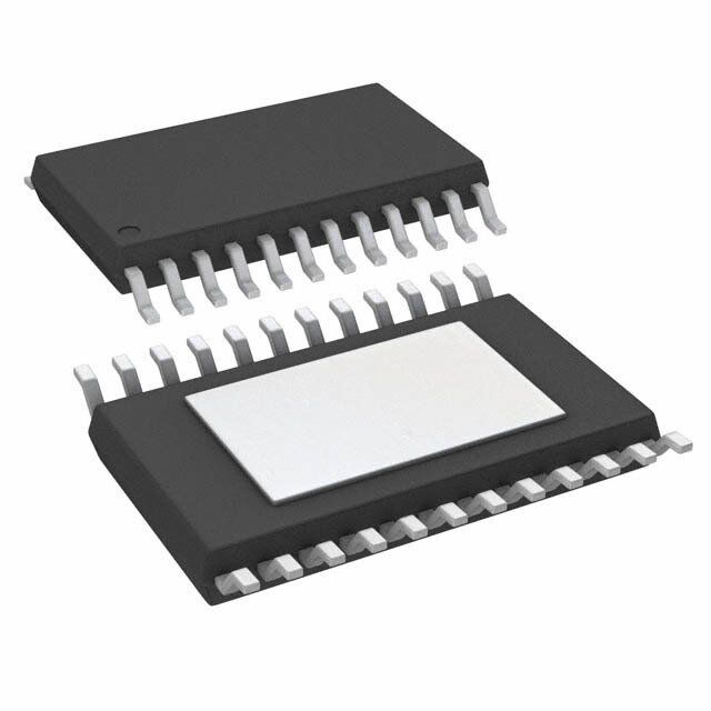
| 产品图片 |
|
| rohs | 符合RoHS无铅 / 符合限制有害物质指令(RoHS)规范要求 |
| 产品系列 | 电源管理 IC,低压差稳压器,Texas Instruments TPS70448PWP- |
| 数据手册 | |
| 产品型号 | TPS70448PWP |
| 产品目录页面 | |
| 产品种类 | 低压差稳压器 |
| 供应商器件封装 | 24-HTSSOP |
| 其它名称 | 296-8028-5 |
| 包装 | 管件 |
| 单位重量 | 98.100 mg |
| 参考电压 | 1.22 V |
| 商标 | Texas Instruments |
| 回动电压—最大值 | 250 mV at 1 A |
| 安装类型 | 表面贴装 |
| 安装风格 | SMD/SMT |
| 封装 | Tube |
| 封装/外壳 | 24-TSSOP(0.173",4.40mm 宽)裸焊盘 |
| 封装/箱体 | HTSSOP-24 |
| 工作温度 | -40°C ~ 125°C |
| 工厂包装数量 | 60 |
| 最大功率耗散 | 4.58 W |
| 最大工作温度 | + 125 C |
| 最大输入电压 | 6 V |
| 最小工作温度 | - 40 C |
| 最小输入电压 | + 2.7 V |
| 标准包装 | 60 |
| 电压-跌落(典型值) | 0.16V @ 1A,- |
| 电压-输入 | 2.7 V ~ 6 V |
| 电压-输出 | 3.3V,1.5V |
| 电压调节准确度 | 2 % |
| 电流-输出 | 1A,2A |
| 电流-限制(最小值) | - |
| 稳压器拓扑 | 正,固定式 |
| 稳压器数 | 2 |
| 系列 | TPS70448 |
| 线路调整率 | 0.01 % / V |
| 负载调节 | 1 mV |
| 输入偏压电流—最大 | 0.185 mA |
| 输出电压 | 3.3 V, 1.5 V |
| 输出电流 | 1 A |
| 输出端数量 | 2 Output |
| 输出类型 | Fixed |


PDF Datasheet 数据手册内容提取
TPS70445, TPS70448 TPS70451, TPS70458 TPS70402 www.ti.com SLVS307F–SEPTEMBER2000–REVISEDAPRIL2010 DUAL-OUTPUT, LOW DROPOUT VOLTAGE REGULATORS WITH INTEGRATED SVS FOR SPLIT VOLTAGE SYSTEMS CheckforSamples:TPS70445,TPS70448,TPS70451,TPS70458,TPS70402 FEATURES DESCRIPTION 1 • DualOutputVoltagesforSplit-Supply The TPS704xx family of devices consists of 23 Applications dual-output, low-dropout voltage regulators with • IndependentEnableFunctions(SeePart integrated SVS (RESET, POR, or power on reset) NumberTPS703xxforSequencedOutputs) and power good (PG) functions. These devices are capable of supplying 1 A and 2 A by regulator 1 and • OutputCurrentRangeof1AonRegulator1 regulator 2 respectively. Quiescent current is typically and2AonRegulator2 185 mA at full load. Differentiated features, such as • FastTransientResponse accuracy, fast transient response, SVS supervisory • VoltageOptions:3.3-V/2.5-V,3.3-V/1.8-V, circuit (power on reset), manual reset input, and independent enable functions provide a complete 3.3-V/1.5-V,3.3-V/1.2-V,andDualAdjustable systemsolution. Outputs • OpenDrainPower-OnResetwith120-msDelay PWP PACKAGE (TOP VIEW) • OpenDrainPowerGoodforRegulator1and Regulator2 GND/HEATSINK 1 24 GND/HEATSINK • Ultralow185mA(typ)QuiescentCurrent V 2 23 V IN1 OUT1 • 2mAInputCurrentDuringStandby VIN1 3 22 VOUT1 NC 4 21 V /FB1 • LowNoise:78mV WithoutBypassCapacitor SENSE1 RMS MR 5 20 NC • QuickOutputCapacitorDischargeFeature EN1 6 19 PG1 • OneManualResetInput EN2 7 18 PG2 • 2%AccuracyOverLoadandTemperature RESET 8 17 NC GND 9 16 V /FB2 • UndervoltageLockout(UVLO)Feature SENSE2 V 10 15 V IN2 OUT2 • 24-PinPowerPAD™TSSOPPackage V 11 14 V IN2 OUT2 • ThermalShutdownProtection GND/HEATSINK 12 13 GND/HEATSINK NC = No internal connection TPS70451 PWP I/O 3.3 V 5 V VIN1 VOUT1 0.22mF 22mF VSENSE1 250 kW PG1 250 kW PG1 VIN2 MR MR >2 V <0.7 V 250 kW 0.22mF RESET RESET >2 V EN1 EN1 PG2 PG2 <0.7 V >2 V EN2 EN2 VSENSE2 <0.7 V VOUT2 1.8V Core 47mF 1 Pleasebeawarethatanimportantnoticeconcerningavailability,standardwarranty,anduseincriticalapplicationsofTexas Instrumentssemiconductorproductsanddisclaimerstheretoappearsattheendofthisdatasheet. PowerPADisatrademarkofTexasInstruments. 2 Allothertrademarksarethepropertyoftheirrespectiveowners. 3 PRODUCTIONDATAinformationiscurrentasofpublicationdate. Copyright©2000–2010,TexasInstrumentsIncorporated Products conform to specifications per the terms of the Texas Instruments standard warranty. Production processing does not necessarilyincludetestingofallparameters.
TPS70445, TPS70448 TPS70451, TPS70458 TPS70402 SLVS307F–SEPTEMBER2000–REVISEDAPRIL2010 www.ti.com The TPS704xx family of voltage regulators offers very low dropout voltage and dual outputs. These devices have extremely low noise output performance without using any added filter bypass capacitors and are designed to haveafasttransientresponseandbestablewith47-mFlowESRcapacitors. These devices have fixed 3.3-V/2.5-V, 3.3-V/1.8-V, 3.3-V/1.5-V, 3.3-V/1.2-V, and adjustable voltage options. Regulator 1 can support up to 1 A, and regulator 2 can support up to 2 A. Separate voltage inputs allow the designertoconfigurethesourcepower. Because the PMOS device behaves as a low-value resistor, the dropout voltage is very low (typically 160 mV on regulator 1) and is directly proportional to the output current. Additionally, since the PMOS pass element is a voltage-driven device, the quiescent current is very low and independent of output loading (maximum of 250 mA over the full range of output current and full range of temperature). This LDO family also features a sleep mode; applying a high signal to EN1 or EN2 (enable) shuts down regulator 1 or regulator 2, respectively. When a high signal is applied to both EN1 and EN2, both regulators enter sleep mode, thereby reducing the input current to 2 mAatT =+25°C. J For each regulator, there is an internal discharge transistor to discharge the output capacitor when the regulator isturnedoff(disabled). The PG1 pin reports the voltage condition at V . The PG1 pin can be used to implement a SVS (RESET, OUT1 POR, or power on reset) for the circuitry supplied by regulator 1. The PG2 pin reports the voltage conditions at V .ThePG2pincanbeusedtoimplementaSVS(poweronreset)forthecircuitrysuppliedbyregulator2. OUT2 The TPS704xx features a RESET (SVS, POR, or power on reset). RESET is an active low, open drain output and requires a pull-up resistor for normal operation. When pulled up, RESET goes into a high impedance state (that is, logic high) after a 120-ms delay when both of the following conditions are met. First, V must be above IN1 the undervoltage condition. Second, the manual reset (MR) pin must be in a high impedance state. To monitor V , the PG1 output pin can be connected to MR. To monitor V , the PG2 output pin can be connected to OUT1 OUT2 MR. RESET can be used to drive power on reset or a low-battery indicator. If RESET is not used, it can be left floating. Internal bias voltages are powered by V and require 2.7 V for full functionality. Each regulator input has an IN1 undervoltagelockoutcircuitthatpreventseachoutputfromturningonuntiltherespectiveinputreaches2.5V. 2 SubmitDocumentationFeedback Copyright©2000–2010,TexasInstrumentsIncorporated
TPS70445, TPS70448 TPS70451, TPS70458 TPS70402 www.ti.com SLVS307F–SEPTEMBER2000–REVISEDAPRIL2010 This integrated circuit can be damaged by ESD. Texas Instruments recommends that all integrated circuits be handled with appropriateprecautions.Failuretoobserveproperhandlingandinstallationprocedurescancausedamage. ESDdamagecanrangefromsubtleperformancedegradationtocompletedevicefailure.Precisionintegratedcircuitsmaybemore susceptibletodamagebecauseverysmallparametricchangescouldcausethedevicenottomeetitspublishedspecifications. ORDERINGINFORMATION(1) VOLTAGE(V)(2) PACKAGE- SPECIFIED LEAD TEMPERATURE ORDERING TRANSPORT PRODUCT V V (DESIGNATOR) RANGE(T ) NUMBER MEDIA,QUANTITY OUT1 OUT2 J TPS70402PWP Tube,60 TPS70402 Adjustable Adjustable HTSSOP-24(PWP) –40°Cto+125°C TPS70402PWPR TapeandReel,2000 TPS70445PWP Tube,60 TPS70445 3.3V 1.2V HTSSOP-24(PWP) –40°Cto+125°C TPS70445PWPR TapeandReel,2000 TPS70448PWP Tube,60 TPS70448 3.3V 1.5V HTSSOP-24(PWP) –40°Cto+125°C TPS70448PWPR TapeandReel,2000 TPS70451PWP Tube,60 TPS70451 3.3V 1.8V HTSSOP-24(PWP) –40°Cto+125°C TPS70451PWPR TapeandReel,2000 TPS70458PWP Tube,60 TPS70458 3.3V 2.5V HTSSOP-24(PWP) –40°Cto+125°C TPS70458PWPR TapeandReel,2000 (1) Forthemostcurrentpackageandorderinginformation,seethePackageOptionAddendumattheendofthisdocument,orvisitthe deviceproductfolderatti.com. (2) Forfixed1.20Voperation,tieFBtoOUT. ABSOLUTE MAXIMUM RATINGS(1) Overoperatingfree-airtemperaturerange(unlessotherwisenoted). TPS704xx UNIT Inputvoltagerange:V ,V (2) –0.3to+7 V IN1 IN2 VoltagerangeatEN1,EN2 –0.3to+7 V Outputvoltagerange(V ,V ) 5.5 V OUT1 SENSE1 Outputvoltagerange(V ,V ) 5.5 V OUT2 SENSE2 MaximumRESET,PG1,PG2voltage 7 V MaximumMRvoltage V V IN1 Peakoutputcurrent Internallylimited — Continuoustotalpowerdissipation SeeDissipationRatingsTable — Operatingvirtualjunctiontemperaturerange,T –40to+150 °C J Storagetemperaturerange,T –65to+150 °C stg ESDrating,HBM 2 kV (1) Stressesbeyondthoselistedunderabsolutemaximumratingsmaycausepermanentdamagetothedevice.Thesearestressratings only,andfunctionaloperationofthedeviceattheseoranyotherconditionsbeyondthoseindicatedunderrecommendedoperating conditionsisnotimplied.Exposuretoabsolute-maximum-ratedconditionsforextendedperiodsmayaffectdevicereliability. (2) Allvoltagesaretiedtonetworkground. Copyright©2000–2010,TexasInstrumentsIncorporated SubmitDocumentationFeedback 3
TPS70445, TPS70448 TPS70451, TPS70458 TPS70402 SLVS307F–SEPTEMBER2000–REVISEDAPRIL2010 www.ti.com DISSIPATION RATINGS DERATING PACKAGE AIRFLOW(CFM) T ≤+25°C T =+70°C T =+85°C A FACTOR A A 0 3.067W 30.67mW/°C 1.687W 1.227W PWP(1) 250 4.115W 41.15mW/°C 2.265W 1.646W (1) Thisparameterismeasuredwiththerecommendedcopperheatsinkpatternona4-layerPCB,1oz.copperona4-inby4-inground layer.Formoreinformation,refertoTItechnicalbriefSLMA002. RECOMMENDED OPERATING CONDITIONS Overoperatingtemperaturerange(unlessotherwisenoted). MIN MAX UNIT Inputvoltage,V (1)(regulator1and2) 2.7 6 V I Outputcurrent,I (regulator1) 0 1 A O Outputcurrent,I (regulator2) 0 2 A O Outputvoltagerange(foradjustableoption) 1.22 5.5 V Operatingvirtualjunctiontemperature,T –40 +125 °C J (1) Tocalculatetheminimuminputvoltageformaximumoutputcurrent,usethefollowingequation:V =V +V . I(min) O(max) DO(maxload) 4 SubmitDocumentationFeedback Copyright©2000–2010,TexasInstrumentsIncorporated
TPS70445, TPS70448 TPS70451, TPS70458 TPS70402 www.ti.com SLVS307F–SEPTEMBER2000–REVISEDAPRIL2010 ELECTRICAL CHARACTERISTICS Overrecommendedoperatingjunctiontemperaturerange(T =–40°Cto+125°C),V orV =V +1V,I =1mA, J IN1 IN2 OUT(nom) O EN=0V,C =22mF,andC =47mF(unlessotherwisenoted). OUT1 OUT2 PARAMETER TESTCONDITIONS MIN TYP MAX UNIT 2.7V<V <6V, Reference T =+25°ICN FBconnectedtoVO 1.22 J voltage 2.7V<V <6V, FBconnectedtoV 1.196 1.244 IN O 1.2VOutput 2.7V<VIN<6V, TJ=+25°C 1.2 (VOUT2) 2.7V<VIN<6V, 1.176 1.224 1.5VOutput 2.7V<VIN<6V, TJ=+25°C 1.5 Output VO voltage (1), (VOUT2) 2.7V<VIN<6V, 1.47 1.53 V (2) 1.8VOutput 2.8V<VIN<6V, TJ=+25°C 1.8 (VOUT2) 2.8V<VIN<6V, 1.764 1.836 2.5VOutput 3.5V<VIN<6V, TJ=+25°C 2.5 (VOUT2) 3.5V<VIN<6V, 2.45 2.55 3.3VOutput 4.3V<VIN<6V, TJ=+25°C 3.3 (VOUT2) 4.3V<VIN<6V, 3.234 3.366 Quiescentcurrent(GNDcurrent)for See (2) T =+25°C 185 J regulator1andregulator2,EN1=EN2 mA =0V(1) See (2) 250 Ofourtrpeugtuvlaotlotarg1ealinnderreegguullaattoiorn2(∆(3V)O/VO) VVO++11VV<<VVIN≤≤66VV, T(1J)=+25°C(1) 0.01 0.1 %V O IN LoadregulationforV andV T =+25°C 1 mV OUT1 OUT2 J Outputnoise Regulator1 79 V voltage BW=300Hzto50kHz, C =33mF,T =+25°C mV n O J RMS (TPS70451) Regulator2 77 Regulator1 1.75 2.2 Outputcurrentlimit V =0V A OUT Regulator2 3.8 4.5 Thermalshutdownjunctiontemperature +150 °C II Standby Regulator1 EN1=VIN,EN2=VIN TJ=+25°C 1 2 mA (standby) current Regulator2 EN1=V ,EN2=V 10 IN IN Power- Regulator1 f=1kHz T =+25°C(1) 65 J supplyripple PSRR dB rejection Regulator2 f=1kHz T =+25°C(1) 60 J (TPS70451) RESETTerminal MinimuminputvoltageforvalidRESET I =300mA, V ≤0.8V 1.0 1.3 V RESET (RESET) t RESETpulseduration 80 120 160 ms (RESET) Outputlowvoltage V =3.5V, I =1mA 0.15 0.4 V IN (RESET) Leakagecurrent V =6V 1 mA (RESET) (1) Minimuminputoperatingvoltageis2.7VorV +1V,whicheverisgreater.Maximuminputvoltage=6V,minimumoutput O(typ) current=1mA. (2) I =1mAto1AforRegulator1and1mAto2AforRegulator2. O (V -2.7) Line regulation (mV) = (%/V) xV Imax x 1000 (3) IfV <1.8VthenV =6V,V =2.7V: o 100 O Imax Imin [V -(V + 1)] Line regulation (mV) = (%/V) xV Imax o x 1000 IfV >2.5VthenV =6V,V =V +1V: o 100 O Imax Imin O Copyright©2000–2010,TexasInstrumentsIncorporated SubmitDocumentationFeedback 5
TPS70445, TPS70448 TPS70451, TPS70458 TPS70402 SLVS307F–SEPTEMBER2000–REVISEDAPRIL2010 www.ti.com ELECTRICAL CHARACTERISTICS (continued) Overrecommendedoperatingjunctiontemperaturerange(T =–40°Cto+125°C),V orV =V +1V, J IN1 IN2 OUT(nom) I =1mA, O EN=0V,C =22mF,andC =47mF(unlessotherwisenoted). OUT1 OUT2 PARAMETER TESTCONDITIONS MIN TYP MAX UNIT V /V Terminal IN1 IN2 UVLOthreshold 2.4 2.65 V UVLOhysteresis 110 mV PG1/PG2Terminal MinimuminputvoltageforvalidPGx I =300mA, V ≤0.8V 1.0 1.3 V (PGx) (PGx) Tripthresholdvoltage V decreasing 92 95 98 %V O OUT Hysteresisvoltage MeasuredatV 0.5 %V O OUT t Risingedgedeglitch 30 ms r(PGx) Outputlowvoltage V =2.7V, I =1mA 0.15 0.4 V IN (PGx) Leakagecurrent V =6V 1 mA (PGx) EN1/EN2Terminal High-levelENxinputvoltage 2 V Low-levelENxinputvoltage 0.7 V Inputcurrent(ENx) –1 1 mA MRTerminal High-levelinputvoltage 2 V Low-levelinputvoltage 0.7 V Pull-upcurrentsource 6 mA V Terminal OUT1 I =1A,V =3.2V T =+25°C 160 Dropoutvoltage(4) O IN1 J mV I =1A,V =3.2V 250 O IN1 Peakoutputcurrent 2mspulsewidth 1.2 A Dischargetransistorcurrent V =1.5V 7.5 mA OUT1 V Terminal OUT2 Peakoutputcurrent 2mspulsewidth 3 A Dischargetransistorcurrent V =1.5V 7.5 mA OUT2 FBTerminal Inputcurrent:TPS70402 FB=1.8V 1 mA (4) Inputvoltage(V orV )=V –100mV.For1.5-V,1.8-V,and2.5-Vregulators,thedropoutvoltageislimitedbyinputvoltage IN1 IN2 O(typ) range.The3.3-Vregulatorinputissetto3.2Vtoperformthistest. 6 SubmitDocumentationFeedback Copyright©2000–2010,TexasInstrumentsIncorporated
TPS70445, TPS70448 TPS70451, TPS70458 TPS70402 www.ti.com SLVS307F–SEPTEMBER2000–REVISEDAPRIL2010 DEVICE INFORMATION FixedVoltageVersion VIN1 (2 Pins) VOUT1(2 Pins) UVLO1 - Comp Current 10kW Sense ENA_1 VSENSE1 2.5 V + (see Note A) - + ENA_1 GND Reference Vref Thermal Shutdown Vref PG1 VSENSE1 - Rising Edge 0.95 x Vref + Deglitch VIN1 PG1 Comp MR RESET 120 ms Delay EN1 ENA_1 PG2 PG2 Comp VSENSE2 - Rising Edge 0.95 x Vref + Deglitch ENA_2 Vref FB2 EN2 - + UVLO2 ENA_2 Comp VSENSE2 2.5 V + Current ENA_2 (see Note A) - Sense 10kW VIN2(2 Pins) VOUT2(2 Pins) A. For most applications, V and V should be externally connected to V and V , respectively, as SENSE1 SENSE2 OUT1 OUT2 close as possible to the device. For other implementations, refer to SENSE terminal connection discussion in the ApplicationInformationsection. Copyright©2000–2010,TexasInstrumentsIncorporated SubmitDocumentationFeedback 7
TPS70445, TPS70448 TPS70451, TPS70458 TPS70402 SLVS307F–SEPTEMBER2000–REVISEDAPRIL2010 www.ti.com AdjustableVoltageVersion VIN1 (2 Pins) VOUT1(2 Pins) UVLO1 Comp Current - Sense ENA_1 FB1 2.5 V + (see Note A) - + ENA_1 GND Reference Vref FB1 Thermal Shutdown Vref PG1 FB1 - Rising Edge 0.95 x Vref + Deglitch VIN1 PG1 Comp MR RESET 120 ms Delay ENA_1 EN1 PG2 PG2 Comp FB2 - Rising Edge 0.95 x Vref + Deglitch ENA_2 Vref FB2 EN2 - + UVLO2 ENA_2 Comp FB2 2.5 V + Current ENA_2 (see Note A) Sense - VIN2(2 Pins) VOUT2(2 Pins) A. For most applications, FB1 and FB2 should be externally connected to resistor dividers as close as possible to the device. For other implementations, refer to FB terminals connection discussion in the Application Information section. 8 SubmitDocumentationFeedback Copyright©2000–2010,TexasInstrumentsIncorporated
TPS70445, TPS70448 TPS70451, TPS70458 TPS70402 www.ti.com SLVS307F–SEPTEMBER2000–REVISEDAPRIL2010 RESETTimingDiagram VIN1 VUVLO VUVLO VRES VRES (see Note A) t MRInput t RESETOutput Output 120 ms 120 ms Output Undefined Delay Delay Undefined t NOTE A: V is the minimum input voltage for a valid R E S E T . The symbolV is not currently listed within EIA or JEDEC RES RES standards for semiconductor symbology. PG1TimingDiagram VIN1 VUVLO VUVLO VPG1 VPG (see Note A) t VOUT1 VIT+ Threshold (see Note B) Voltage VIT- (see Note B) t PG1 Output PG1 Output Output Undefined Undefined t NOTES A: V is the minimum input voltage for a valid PG. The symbolV is not currently listed within EIA or JEDEC PG1 PG1 standards for semiconductor symbology. NOTES B:V trip voltage is typically 5% lower than the output voltage (95%V ). V to V is the hysteresis voltage. IT- O IT- IT+ Copyright©2000–2010,TexasInstrumentsIncorporated SubmitDocumentationFeedback 9
TPS70445, TPS70448 TPS70451, TPS70458 TPS70402 SLVS307F–SEPTEMBER2000–REVISEDAPRIL2010 www.ti.com PG2TimingDiagram(assumingV alreadypoweredup) IN1 VIN2 t VOUT2 VIT+ Threshold (see Note A) Voltage VIT- (see Note A) t PG2 Output t NOTE A: V trip voltage is typically 5% lower than the output voltage (95%V ). V to V is the hysteresis voltage. IT- O IT- IT+ TERMINALFUNCTIONS TERMINAL I/O DESCRIPTION NAME NO. EN1 6 I ActivelowenableforV OUT1 EN2 7 I ActivelowenableforV OUT2 GND 9 — Ground GND/HEATSI 1,12,13,24 — Ground/heatsink NK MR 5 I Manualresetinput,activelow,pulledupinternally NC 4,17,20 — Noconnection PG1 19 O Opendrainoutput,lowwhenV voltageislessthan95%ofthenominalregulatedvoltage OUT1 PG2 18 O Opendrainoutput,lowwhenV voltageislessthan95%ofthenominalregulatedvoltage OUT2 RESET 8 O Opendrainoutput,SVS(power-onreset)signal,activelow V 2,3 I Inputvoltageofregulator1 IN1 V 10,11 I Inputvoltageofregulator2 IN2 V 22,23 O Outputvoltageofregulator1 OUT1 V 14,15 O Outputvoltageofregulator2 OUT2 V /FB1 21 I Regulator1outputvoltagesense/regulator1feedbackforadjustable SENSE1 V /FB2 16 I Regulator2outputvoltagesense/regulator2feedbackforadjustable SENSE2 10 SubmitDocumentationFeedback Copyright©2000–2010,TexasInstrumentsIncorporated
TPS70445, TPS70448 TPS70451, TPS70458 TPS70402 www.ti.com SLVS307F–SEPTEMBER2000–REVISEDAPRIL2010 Detailed Description The TPS704xx low dropout regulator family provides dual regulated output voltages with independent enable functions. These devices provide fast transient response and high accuracy with small output capacitors, while drawing low quiescent current. Other features are integrated SVS (power-on reset, RESET) and power good (PG1, PG2) that monitor output voltages and provide logic output to the system. These differentiated features provideacompletepowersolution. The TPS704xx, unlike many other LDOs, features very low quiescent current that remains virtually constant even with varying loads. Conventional LDO regulators use a PNP pass element, the base current of which is directly proportional to the load current through the regulator (I = I /b). The TPS704xx uses a PMOS transistor to pass B C current; because the gate of the PMOS is voltage-driven, operating current is low and stable over the full load range. Pin Functions Enable(EN1,EN2) The EN terminals are inputs that enable or shut down each respective regulator. If EN is at a voltage high signal, therespectiveregulatorisinshutdownmode.WhenENgoestovoltagelow,therespectiveregulatorisenabled. Power-Good(PG1,PG2) The PG terminals are open drain, active high output terminals that indicate the status of each respective regulator. When V reaches 95% of its regulated voltage, PG1 goes to a high impedance state. When V OUT1 OUT2 reaches 95% of its regulated voltage, PG2 goes to a high impedance state. Each PG goes to a low impedance state when its respective output voltage is pulled below 95% (that is, goes to an overload condition) of its regulatedvoltage.TheopendrainoutputsofthePGterminalsrequireapull-upresistor. ManualResetPin MR is an active low input terminal used to trigger a reset condition. When MR is pulled to logic low, a POR (RESET) occurs. The terminal has a 6-mA pull-up current to V ; however, it is recommended that the pin be IN1 pulledhightoV whenitisnotused. IN1 Sense(V ,V ) SENSE1 SENSE2 The sense terminals of fixed-output options must be connected to the regulator outputs, and the connection should be as short as possible. Internally, the sense terminal connects to high-impedance, wide-bandwidth amplifiersthrougharesistor-dividernetworkandnoisepickupfeedsthroughtotheregulatoroutput.Itisessential to route the sense connection in such a way as to minimize or avoid noise pickup. Adding RC networks between sense terminals and V terminals to filter noise is not recommended because these networks can cause the OUT regulatorstooscillate. Copyright©2000–2010,TexasInstrumentsIncorporated SubmitDocumentationFeedback 11
TPS70445, TPS70448 TPS70451, TPS70458 TPS70402 SLVS307F–SEPTEMBER2000–REVISEDAPRIL2010 www.ti.com FB1andFB2 FB1 and FB2 are input terminals used for adjustable-output devices and must be connected to the external feedback resistor divider. FB1 and FB2 connections should be as short as possible. It is essential to route them in such a way as to minimize or avoid noise pickup. Adding RC networks between FB terminals and V OUT terminalstofilternoiseisnotrecommendedbecausethesenetworkscancausetheregulatorstooscillate. RESETIndicator RESET is an active low, open drain output and requires a pullup resistor for normal operation. When pulled up, RESET goes into a high impedance state (that is, logic high) after a 120-ms delay when both of the following conditions are met. First, V must be above the undervoltage condition. Second, the manual reset (MR) pin IN1 must be in a high impedance state. To monitor V , the PG1 output pin can be connected to MR. To monitor OUT1 V ,thePG2outputpincanbeconnectedtoMR.IfRESETisnotused,itcanbeleftfloating. OUT2 V andV IN1 IN2 V andV areinputstoeachregulator.InternalbiasvoltagesarepoweredbyV . IN1 IN2 IN1 V andV OUT1 OUT2 V andV areoutputterminalsofeachregulator. OUT1 OUT2 12 SubmitDocumentationFeedback Copyright©2000–2010,TexasInstrumentsIncorporated
TPS70445, TPS70448 TPS70451, TPS70458 TPS70402 www.ti.com SLVS307F–SEPTEMBER2000–REVISEDAPRIL2010 TYPICAL CHARACTERISTICS TableofGraphs FIGURE vsOutputcurrent Figure1andFigure2 V Outputvoltage O vsJunctiontemperature Figure3toFigure4 Groundcurrent vsJunctiontemperature Figure5 PSRR Power-supplyrejectionratio vsFrequency Figure6toFigure9 Outputspectralnoisedensity vsFrequency Figure10toFigure13 Z Outputimpedance vsFrequency Figure14toFigure17 O vsTemperature Figure18andFigure19 Dropoutvoltage vsInputvoltage Figure20andFigure21 Loadtransientresponse Figure22andFigure23 Linetransientresponse(V ) Figure24 OUT1 Linetransientresponse(V ) Figure25 OUT2 V Outputvoltage vsTime(start-up) Figure26andFigure27 O Equivalentseriesresistance(ESR) vsOutputcurrent Figure29toFigure32 TPS70451 TPS70451 OUTPUTVOLTAGE OUTPUTVOLTAGE vs vs OUTPUTCURRENT OUTPUTCURRENT 3.33 1.815 V = 2.8 V IN2 V = 4.3 V IN1 T = 25°C 3.32 T = 25°C 1.81 J J V OUT2 V V OUT1 V e- 3.31 e- 1.805 g g a a olt olt V V ut 3.30 ut 1.8 p p ut ut O O - 3.29 - 1.795 O O V V 3.28 1.79 3.27 1.785 0 200 400 600 800 1000 0 500 1000 1500 2000 IO-Output Current-mA IO-Output Current-mA Figure1. Figure2. Copyright©2000–2010,TexasInstrumentsIncorporated SubmitDocumentationFeedback 13
TPS70445, TPS70448 TPS70451, TPS70458 TPS70402 SLVS307F–SEPTEMBER2000–REVISEDAPRIL2010 www.ti.com TYPICAL CHARACTERISTICS (continued) TPS70451 TPS70451 OUTPUTVOLTAGE OUTPUTVOLTAGE vs vs JUNCTIONTEMPERATURE JUNCTIONTEMPERATURE 1.834 3.354 VIN1= 4.3 V VIN2= 2.8 V VOUT1 VOUT2 1.824 3.334 V V 1.814 - - Voltage 3.314 IO= 1 mA Voltage 1.804 IO= 2 A Output 3.294 IO= 1 A Output 1.794 IO= 1 mA - - O 3.274 O V V 1.784 3.254 1.774 3.234 1.764 -40-25 -10 5 20 35 50 65 80 95 110 125 -40-25 -10 5 20 35 50 65 80 95 110 125 TJ-Junction Temperature-°C TJ-Junction Temperature-°C Figure3. Figure4. TPS70451 GROUNDCURRENT vs JUNCTIONTEMPERATURE 210 Regulator 1 and Regulator 2 200 I = 1 mA OUT1 I = 1 mA OUT2 A m 190 - nt e urr 180 IOUT1= 1 A C d IOUT2= 2 A n u ro 170 G 160 150 -40-25 -10 5 20 35 50 65 80 95 110 125 T -Junction Temperature-°C J Figure5. 14 SubmitDocumentationFeedback Copyright©2000–2010,TexasInstrumentsIncorporated
TPS70445, TPS70448 TPS70451, TPS70458 TPS70402 www.ti.com SLVS307F–SEPTEMBER2000–REVISEDAPRIL2010 TYPICAL CHARACTERISTICS (continued) TPS70451 TPS70451 POWER-SUPPLYREJECTIONRATIO POWER-SUPPLYREJECTIONRATIO vs vs FREQUENCY FREQUENCY -10 0 VIN1= 4.3 V VIN1= 4.3 V dB -20 VOUT1 = 3.3 V dB -10 VOUT1 = 3.3 V Ratio- -30 ICOO== 1 202 mmAF Ratio- -20 ICOO== 1 2 A2mF n n -30 o o ecti -40 ecti -40 ej ej R R y -50 y -50 pl pl p p Su -60 Su -60 er er w w -70 o o P -70 P - - -80 R R R R PS -80 PS -90 -90 -100 10 100 1 k 10 k 100 k 1M 10 100 1 k 10 k 100 k 1M f-Frequency-Hz f-Frequency-Hz Figure6. Figure7. TPS70451 TPS70451 POWER-SUPPLYREJECTIONRATIO POWER-SUPPLYREJECTIONRATIO vs vs FREQUENCY FREQUENCY 0 0 V = 2.8 V V = 2.8 V IN2 IN2 dB -10 VOUT2 = 1.8 V dB -10 VOUT2 = 1.8 V - - Ratio -20 ICOO== 1 407 mmAF Ratio -20 ICOO== 2 4 A7mF n -30 n -30 o o ecti -40 ecti -40 ej ej R R y -50 y -50 pl pl p p Su -60 Su -60 er er w -70 w -70 o o P P - -80 - -80 R R R R PS -90 PS -90 -100 -100 10 100 1 k 10 k 100 k 1M 10 100 1 k 10 k 100 k 1M f-Frequency-Hz f-Frequency-Hz Figure8. Figure9. Copyright©2000–2010,TexasInstrumentsIncorporated SubmitDocumentationFeedback 15
TPS70445, TPS70448 TPS70451, TPS70458 TPS70402 SLVS307F–SEPTEMBER2000–REVISEDAPRIL2010 www.ti.com TYPICAL CHARACTERISTICS (continued) OUTPUTSPECTRALNOISEDENSITY OUTPUTSPECTRALNOISEDENSITY vs vs FREQUENCY FREQUENCY 10 10 VIN1= 4.3 V VIN2= 2.8 V z VOUT1= 3.3 V z VOUT2= 1.8 V H H ÖV/ COUT1= 22mF ÖV/ COUT2= 47mF - m IO= 10 mA - m IO= 10 mA sity 1 TJ = 25°C sity 1 TJ = 25°C n n e e D D e e s s oi oi N N al al ctr 0.1 ctr 0.1 e e p p S S ut ut p p ut ut O O 0.01 0.01 100 1 k 10 k 100 k 100 1 k 10 k 100 k f-Frequency-Hz f-Frequency-Hz Figure10. Figure11. OUTPUTSPECTRALNOISEDENSITY OUTPUTSPECTRALNOISEDENSITY vs vs FREQUENCY FREQUENCY 10 10 VIN1= 4.3 V VIN2= 2.8 V Hz VOUT1= 3.3 V Hz VOUT2= 1.8 V ÖV/ COUT1= 22mF ÖV/ COUT2= 47mF - m IO= 1 mA - m IO= 2 A sity 1 TJ = 25°C sity 1 TJ = 25°C n n e e D D e e s s oi oi N N al al ctr 0.1 ctr 0.1 e e p p S S ut ut p p ut ut O O 0.01 0.01 100 1 k 10 k 100 k 100 1 k 10 k 100 k f-Frequency-Hz f-Frequency-Hz Figure12. Figure13. 16 SubmitDocumentationFeedback Copyright©2000–2010,TexasInstrumentsIncorporated
TPS70445, TPS70448 TPS70451, TPS70458 TPS70402 www.ti.com SLVS307F–SEPTEMBER2000–REVISEDAPRIL2010 TYPICAL CHARACTERISTICS (continued) OUTPUTIMPEDANCE OUTPUTIMPEDANCE vs vs FREQUENCY FREQUENCY V = 3.3 V V = 3.3 V OUT1 OUT1 I = 1 A I = 10 mA O O C = 22mF C = 22mF O O W 1 W 1 - - e e c c n n a a d d e e p p m 0.1 m 0.1 ut I ut I p p ut ut O O - - ZO 0.01 ZO 0.01 10 100 1 k 10 k 100 k 1M 10M 10 100 1 k 10 k 100 k 1M 10M f-Frequency-Hz f-Frequency-Hz Figure14. Figure15. OUTPUTIMPEDANCE OUTPUTIMPEDANCE vs vs FREQUENCY FREQUENCY V = 1.8 V V = 1.8 V OUT2 OUT2 I = 10 mA I = 2 A O O C = 47mF C = 47mF O O W 1 W 1 - - e e c c n n a a d d e e p p m 0.1 m 0.1 ut I ut I p p ut ut O O - - ZO 0.01 ZO 0.01 10 100 1 k 10 k 100 k 1M 10M 10 100 1 k 10 k 100 k 1M 10M f-Frequency-Hz f-Frequency-Hz Figure16. Figure17. Copyright©2000–2010,TexasInstrumentsIncorporated SubmitDocumentationFeedback 17
TPS70445, TPS70448 TPS70451, TPS70458 TPS70402 SLVS307F–SEPTEMBER2000–REVISEDAPRIL2010 www.ti.com TYPICAL CHARACTERISTICS (continued) TPS70451 TPS70451 DROPOUTVOLTAGE DROPOUTVOLTAGE vs vs TEMPERATURE TEMPERATURE 250 25 VOUT1 VOUT1 VIN1= 3.2 V VIN1= 3.2 V 200 20 I = 1 A O I = 100 mA V V O m m - - e 150 e 15 g g a a olt olt V V out 100 out 10 p p o o Dr Dr 50 5 I = 1 mA O I = 10 mA O 0 0 -40-25 -10 5 20 35 50 65 80 95 110 125 -40-25 -10 5 20 35 50 65 80 95 110 125 T-Temperature-°C T-Temperature-°C Figure18. Figure19. TPS70402 TPS70402 DROPOUTVOLTAGE DROPOUTVOLTAGE vs vs INPUTVOLTAGE INPUTVOLTAGE 300 300 VOUT1 VOUT2 IO= 1 A IO= 2 A 250 250 T = 125°C J V TJ = 125°C V m 200 m 200 - - TJ = 25°C e e ag TJ = 25°C ag olt 150 olt 150 V V ut ut o o op 100 op 100 TJ =-40°C Dr T =-40°C Dr J 50 50 0 0 2.5 3 3.5 4 4.5 5 5.5 2.5 3 3.5 4 4.5 5 5.5 V -Input Voltage-V V -Input Voltage-V I I Figure20. Figure21. 18 SubmitDocumentationFeedback Copyright©2000–2010,TexasInstrumentsIncorporated
TPS70445, TPS70448 TPS70451, TPS70458 TPS70402 www.ti.com SLVS307F–SEPTEMBER2000–REVISEDAPRIL2010 TYPICAL CHARACTERISTICS (continued) LOADTRANSIENTRESPONSE LOADTRANSIENTRESPONSE A A Current- 1 VVCIOONU1=T =21 24=. m33F .V3 V Current- 2 VICOOO=U= T2 42 A7= m1F.8 V ut 0.5 ut 1 p p ut ut O 0 O 0 - - O O I I 50 V V n m n m e i - 0 e i - 50 g e g e n g n g a a a a Ch olt -50 Ch olt 0 V V -Out -Out DV utp -100 DV utp -50 O O 0 0.2 0.4 0.6 0.8 1 1.2 1.4 1.6 1.8 2 0 0.2 0.4 0.6 0.8 1 1.2 1.4 1.6 1.8 2 t-Time-ms t-Time-ms Figure22. Figure23. LINETRANSIENTRESPONSE LINETRANSIENTRESPONSE V VOUT1= 3.3 V V VOUT2= 1.8 V - - ge 5.3 IO= 1 A ge 3.8 IO= 2 A a C = 22mF a C = 47mF olt O olt O V V ut ut p p In 4.3 In 2.8 - - VI VI V V n m n m e i - 50 e i - 100 g e g e n g n g a a a a Ch olt 0 Ch olt 0 V V -Out -Out DV utp 50 DV utp 100 O O 100 200 0 20 40 60 80 100 120 140 160 180 200 0 20 40 60 80 100 120 140 160 180 20 t-Time-ms t-Time-ms Figure24. Figure25. Copyright©2000–2010,TexasInstrumentsIncorporated SubmitDocumentationFeedback 19
TPS70445, TPS70448 TPS70451, TPS70458 TPS70402 SLVS307F–SEPTEMBER2000–REVISEDAPRIL2010 www.ti.com TYPICAL CHARACTERISTICS (continued) OUTPUTVOLTAGEANDENABLEVOLTAGE OUTPUTVOLTAGEANDENABLEVOLTAGE vs vs TIME(START-UP) TIME(START-UP) 4 V V - - Voltage 32 VIOO=U T11 A= 3.3 V Voltage 2 Output 1 CVION1= =2 24.m3F V Output 1 EN2= High - - O O V 0 V 0 V = 1.8 V OUT2 V V I = 2 A - - O Voltage 5 Voltage 5 CVEINON12== =4 7H2.im8gF hV Enable 0 Enable 0 0 0.2 0.4 0.6 0.8 1 1.2 1.4 1.6 1.8 2 0 0.2 0.4 0.6 0.8 1 1.2 1.4 1.6 1.8 2 t-Time-ms t-Time-ms Figure26. Figure27. VIN IN To Load OUT + C EN OUT RL GND ESR Figure28.TestCircuitforTypicalRegionsofStability 20 SubmitDocumentationFeedback Copyright©2000–2010,TexasInstrumentsIncorporated
TPS70445, TPS70448 TPS70451, TPS70458 TPS70402 www.ti.com SLVS307F–SEPTEMBER2000–REVISEDAPRIL2010 TYPICAL CHARACTERISTICS (continued) TYPICALREGIONOFSTABILITY TYPICALREGIONOFSTABILITY EQUIVALENTSERIESRESISTANCE(1) EQUIVALENTSERIESRESISTANCE(1) vs vs OUTPUTCURRENT OUTPUTCURRENT 10 10 VOUT1= 3.3 V VOUT1= 3.3 V W CO= 22mF W CO= 220mF - - e e c c an REGION OF INSTABILITY an REGION OF INSTABILITY st st si 1 si 1 e e R R s s e e eri eri S S nt nt e e al al quiv 0.1 50 mW quiv 0.1 E E - - R R S S E E 15 mW 0.01 0.01 0 0.1 0.2 0.3 0.4 0.5 0.6 0.7 0.8 0.9 1 0 0.1 0.2 0.3 0.4 0.5 0.6 0.7 0.8 0.9 1 IO-Output Current-A IO-Output Current-A Figure29. Figure30. TYPICALREGIONOFSTABILITY TYPICALREGIONOFSTABILITY EQUIVALENTSERIESRESISTANCE(1) EQUIVALENTSERIESRESISTANCE(1) vs vs OUTPUTCURRENT OUTPUTCURRENT 10 10 REGION OF INSTABILITY REGION OF INSTABILITY W W - - e e c c an VOUT2= 1.8 V an VOUT2= 1.8 V sist 1 CO= 47mF sist 1 CO= 680mF e e R R s s e e eri eri S S nt nt e e al al quiv 0.1 50 mW quiv 0.1 E E - - R R S S E E 15 mW 0.01 0.01 0 0.1 0.2 0.3 0.4 0.5 0.6 0.7 0.8 0.9 1 0 0.1 0.2 0.3 0.4 0.5 0.6 0.7 0.8 0.9 1 IO-Output Current-A IO-Output Current-A Figure31. Figure32. (1)Equivalentseriesresistance(ESR)referstothetotalseriesresistance,includingtheESRofthecapacitor,any seriesresistanceaddedexternally,andPWBtraceresistancetoC . O Copyright©2000–2010,TexasInstrumentsIncorporated SubmitDocumentationFeedback 21
TPS70445, TPS70448 TPS70451, TPS70458 TPS70402 SLVS307F–SEPTEMBER2000–REVISEDAPRIL2010 www.ti.com THERMAL INFORMATION Thermally-Enhanced TSSOP-24 (PWP— PowerPAD™) The thermally-enhanced PWP package is based on the 24-pin TSSOP, but includes a thermal pad [see Figure33(c)]toprovideaneffectivethermalcontactbetweentheICandtheprintedwiringboard(PWB). Traditionally, surface mount and power have been mutually exclusive terms. A variety of scaled-down TO220-type packages have leads formed as gull wings to make them applicable for surface-mount applications. These packages, however, suffer from several shortcomings: they do not address the very low profile requirements (<2 mm) of many of today’s advanced systems, and they do not offer a pin-count high enough to accommodate increasing integration. On the other hand, traditional low-power surface-mount packages require power-dissipationderatingthatseverelylimitstheusablerangeofmanyhigh-performanceanalogcircuits. The PWP package (thermally-enhanced TSSOP) combines fine-pitch surface-mount technology with thermal performancecomparabletomuchlargerpowerpackages. The PWP package is designed to optimize the heat transfer to the PWB. Because of the very small size and limited mass of a TSSOP package, thermal enhancement is achieved by improving the thermal conduction paths that remove heat from the component. The thermal pad is formed using a lead-frame design (patent pending) and manufacturing technique to provide the user with direct connection to the heat-generating IC. When this pad is soldered or otherwise coupled to an external heat dissipator, high power dissipation in the ultrathin, fine-pitch, surface-mountpackagecanbereliablyachieved. DIE SideView (a) Thermal Pad DIE End View (b) Bottom View (c) Figure33. ViewsofThermally-EnhancedPWPPackage Because the conduction path has been enhanced, power-dissipation capability is determined by the thermal considerations in the PWB design. For example, simply adding a localized copper plane (heat-sink surface), which is coupled to the thermal pad, enables the PWP package to dissipate 2.5 W in free air (reference Figure 35(a), 8 cm2 of copper heat sink and natural convection). Increasing the heat-sink size increases the power dissipation range for the component. The power dissipation limit can be further improved by adding airflow to a PWB/IC assembly (see Figure 34 and Figure 35). The line drawn at 0.3 cm2 in Figure 34 and Figure 35 indicatesperformanceattheminimumrecommendedheat-sinksize,illustratedinFigure36. 22 SubmitDocumentationFeedback Copyright©2000–2010,TexasInstrumentsIncorporated
TPS70445, TPS70448 TPS70451, TPS70458 TPS70402 www.ti.com SLVS307F–SEPTEMBER2000–REVISEDAPRIL2010 The thermal pad is directly connected to the substrate of the IC, which for the TPS704xx series is a secondary electrical connection to device ground. The heat-sink surface that is added to the PWP can be a ground plane or left electrically isolated. In TO220-type surface-mount packages, the thermal connection is also the primary electrical connection for a given terminal which is not always ground. The PWP package provides up to 24 independent leads that can be used as inputs and outputs (Note: leads 1, 12, 13, and 24 are internally connectedtothethermalpadandtheICsubstrate). THERMALRESISTANCE vsCOPPERHEATSINKAREA 150 125 NaturalConvection W 50 ft/min C/ ° - 100 ft/min e c an 100 150 ft/min st si e 200 ft/min R al m er 75 h T - A J Rq 50 250 ft/min 300 ft/min 25 0 0.3 1 2 3 4 5 6 7 8 Copper Heatsink Area-cm2 Figure34. Copyright©2000–2010,TexasInstrumentsIncorporated SubmitDocumentationFeedback 23
TPS70445, TPS70448 TPS70451, TPS70458 TPS70402 SLVS307F–SEPTEMBER2000–REVISEDAPRIL2010 www.ti.com 3.5 3.5 TA= 25°C TA= 55°C 300 ft/min 3 3 W W - 150 ft/min - mit 2.5 mit 2.5 300ft/min Li Li n n atio 2 atio 2 150 ft/min p Natural Convection p si si s s Di 1.5 Di 1.5 er er Natural Convection w w o o P 1 P 1 - - D D P P 0.5 0.5 0 0 0 2 4 6 8 0 2 4 6 8 0.3 Copper Heatsink Size-cm2 0.3 Copper Heatsink Size-cm2 (a) (b) 3.5 TA= 105°C 3 W - mit 2.5 Li n o ati 2 p si s Di 1.5 r 150 ft/min e w 300 ft/min o P 1 - D P Natural Convection 0.5 0 0 2 4 6 8 0.3 Copper Heatsink Size-cm2 (c) Figure35. PowerRatingsofthePWPPackageatAmbientTemperaturesof+25°C,+55°C,and+105°C 24 SubmitDocumentationFeedback Copyright©2000–2010,TexasInstrumentsIncorporated
TPS70445, TPS70448 TPS70451, TPS70458 TPS70402 www.ti.com SLVS307F–SEPTEMBER2000–REVISEDAPRIL2010 Figure 36 is an example of a thermally-enhanced PWB layout for use with the new PWP package. This board configuration was used in the thermal experiments that generated the power ratings shown in Figure 34 and Figure 35. As discussed earlier, copper has been added on the PWB to conduct heat away from the device. R qJA for this assembly is illustrated in Figure 34 as a function of heat-sink area. A family of curves is included to illustratetheeffectofairflowintroducedintothesystem. Heatsink Area 1ozCopper Boardthickness 62mils Board size 3.2 in´3.2 in Board material FR4 Copper trace/heat sink 1 oz Exposed pad mounting 63/67 tin/lead solder Figure36. PWBLayout(IncludingCopperHeatsinkArea)forThermally-EnhancedPWPPackage From Figure 34, R for a PWB assembly can be determined and used to calculate the maximum qJA power-dissipationlimitforthecomponent/PWBassembly,withtheequation: T -T P = Jmax A D(max) R qJA(system) where: • T isthemaximumspecifiedjunctiontemperature(+150°Cabsolutemaximumlimit,+125°Crecommended Jmax operatinglimit)andT istheambienttemperature. (1) A P should then be applied to the internal power dissipated by the TPS704xx regulator. The equation for D(max) calculatingtotalinternalpowerdissipationoftheTPS704xxis: ( ( I ( ( I P = V -V ´I + V ´ Q + V -V ´I + V ´ Q D(total) IN1 OUT1 OUT1 IN1 2 IN2 OUT2 OUT2 IN2 2 (2) Since the quiescent current of the TPS704xx is very low, the second term is negligible, further simplifying the equationto: ( ( ( ( P = V -V ´I + V -V ´I D(total) IN1 OUT1 OUT1 IN2 OUT2 OUT2 (3) For the case where T = +55°C, airflow = 200 ft/min, copper heat-sink area = 4 cm2, the maximum A power-dissipation limit can be calculated. First, from Figure 34, we find the system R is +50°C/W; therefore, qJA themaximumpower-dissipationlimitis: P = TJmax-TA =+125°C-55°C = 1.4 W D(max) R +50°C/W qJA(system) (4) If the system implements a TPS704xx regulator, where V = 5.0V, V = 2.8 V, I = 500 mA, and I = IN1 IN2 OUT1 OUT2 800mA,theinternalpowerdissipationis: ( ( ( ( P = V -V ´I + V -V ´I D(total) IN1 OUT1 OUT1 IN2 OUT2 OUT2 = (5.0-3.3)´0.5 + (2.8-1.8)´0.8 = 1.25 W (5) Copyright©2000–2010,TexasInstrumentsIncorporated SubmitDocumentationFeedback 25
TPS70445, TPS70448 TPS70451, TPS70458 TPS70402 SLVS307F–SEPTEMBER2000–REVISEDAPRIL2010 www.ti.com Comparing P with P reveals that the power dissipation in this example does not exceed the calculated D(total) D(max) limit. When it does, one of two corrective actions should be made: raising the power-dissipation limit by increasingtheairflowortheheat-sinkarea,orloweringtheinternalpowerdissipationoftheregulatorbyreducing the input voltage or the load current. In either case, the above calculations should be repeated with the new system parameters. This parameter is measured with the recommended copper heat sink pattern on a 4-layer PWB, 2 oz. copper traces on 4-in × 4-in ground layer. Simultaneous and continuous operation of both regulator outputsatfullloadmayexceedthepowerdissipationratingofthePWPpackage. Mounting Information The primary requirement is to complete the thermal contact between the thermal pad and the PWB metal. The thermal pad is a solderable surface and is fully intended to be soldered at the time the component is mounted. Althoughvoidinginthethermal-padsolder-connectionisnotdesirable,upto50%voidingisacceptable.Thedata included in Figure 34 and Figure 36 are for soldered connections with voiding between 20% and 50%. The thermalanalysisshowsnosignificantdifferenceresultingfromthevariationinvoidingpercentage. Figure 37 shows the solder-mask land pattern for the PWP package. The minimum recommended heat-sink area is also illustrated. This is simply a copper plane under the body extent of the package, including metal routed underterminals1,12,13,and24. Minimum Recommended LocationofExposed Heatsink Area Thermal Pad on PWP Package Figure37. PWPPackageLandPattern 26 SubmitDocumentationFeedback Copyright©2000–2010,TexasInstrumentsIncorporated
TPS70445, TPS70448 TPS70451, TPS70458 TPS70402 www.ti.com SLVS307F–SEPTEMBER2000–REVISEDAPRIL2010 APPLICATION INFORMATION Sequencing Timing Diagrams TPS704xxPWP (Fixed Output Option) This section provides a number of timing diagrams V VOUT1 showing how this device functions in different IN VIN1 VOUT1 configurations. 0.22mF 22mF V 250 kW Application condition: V and V are tied to the SENSE1 IN1 IN2 same fixed input voltage greater than V . PG2 is UVLO tiedtoMR. PG1 MR EN1 and EN2 are initially high; therefore, both VIN2 MR 250 kW regulators are off, and PG1 and PG2 (tied to MR) are at logic low. Since MR is at logic low, RESET is also 0.22mF RESET RESET at logic low. When EN1 is taken to logic low, V OUT1 turns on. Later, when EN2 is taken to logic low, VOUT2 PG2 PG2 turns on. When V reaches 95% of its regulated EN1 output voltage, PGO1UTg1oes to logic high. When V >2 V EN1 OUT2 reaches 95% of its regulated output voltage, PG2 <0.7 V VSENSE2 (tied to MR) goes to logic high. When VIN1 is greater EN2 than VUVLO and M R (tied to PG2) is at logic high, >2 V EN2 VOUT2 VOUT2 RESET is pulled to logic high after a 120-ms delay. <0.7 V When EN1 and EN2 are returned to logic high, both 47mF devices power down and both PG1, PG2 (tied to MR2),andRESETreturntologiclow. EN2 EN1 95% V OUT2 95% V OUT1 PG2 PG1 MR (PG2 tied toMR) RESET t 1 120 ms NOTES: A. t: Time at which V is greater than V andMRis logic high. 1 IN UVLO B. The timing diagram is not drawn to scale. Figure38. TimingWhenV IsEnabledBeforeV OUT1 OUT2 Copyright©2000–2010,TexasInstrumentsIncorporated SubmitDocumentationFeedback 27
TPS70445, TPS70448 TPS70451, TPS70458 TPS70402 SLVS307F–SEPTEMBER2000–REVISEDAPRIL2010 www.ti.com Application condition: V and V are tied to the IN1 IN2 same fixed input voltage greater than V . MR is TPS704xxPWP UVLO (Fixed Output Option) initiallylogichighbutiseventuallytoggled. VIN VOUT1 V V EN1 and EN2 are initially high; therefore, both IN1 OUT1 regulators are off, and PG1 and PG2 are at logic low. 0.22mF Since VIN1 is greater than VUVLO and MR is at logic VSENSE1 high, RESET is also at logic high. When EN2 is taken 22mF 250 kW to logic low, V turns on. Later, when EN1 is taken OUT2 250 kW to logic low, V turns on. When V reaches OUT1 OUT2 95% of its regulated output voltage, PG2 goes to V IN2 250 kW logic high. When V reaches 95% of its regulated OUT1 output voltage, PG1 goes to logic high. When MR is 0.22mF RESET RESET taken to logic low, RESET is taken low. When MR returns to logic high, RESET returns to logic high PG2 aftera120-msdelay. EN1 PG2 EN1 MR >2 V MR 2 V <0.7 V VSENSE2 0.7 V EN2 >2 V EN2 V VOUT2 <0.7 V OUT2 47mF EN2 EN1 V 95% OUT2 95% V OUT1 PG2 PG1 MR RESET t 1 120 ms NOTES: A. t: Time at which V is greater than V andMRis logic high. 1 IN UVLO B. The timing diagram is not drawn to scale. Figure39. TimingWhenMRisToggled 28 SubmitDocumentationFeedback Copyright©2000–2010,TexasInstrumentsIncorporated
TPS70445, TPS70448 TPS70451, TPS70458 TPS70402 www.ti.com SLVS307F–SEPTEMBER2000–REVISEDAPRIL2010 Application condition: V and V are tied to IN1 IN2 same fixed input voltage greater than V . PG1 is TPS704xxPWP UVLO (Fixed Output Option) tiedtoMR. V V IN OUT1 V EN1 and EN2 are initially high; therefore, both VIN1 OUT1 regulators are off, and PG1 (tied to MR) and PG2 are at logic low. Since MR is at logic low, RESET is also 0.22mF V 22mF SENSE1 at logic low. When EN2 is taken to logic low, VOUT2 250 kW turns on. Later, when EN1 is taken to logic low, V OUT1 PG1 turns on. When V reaches 95% of its regulated OUT2 output voltage, PG2 goes to logic high. When V MR OUT1 V 250 kW reaches 95% of its regulated output voltage, PG1 IN2 goes to logic high. When VIN1 is greater than VUVLO 0.22mF RESET RESET and MR (tied to PG2) is at logic high, RESET is pulled to logic high after a 120-ms delay. When a PG2 fault on VOUT1 causes it to fall below 95% of its EN1 PG2 regulated output voltage, PG1 (tied to MR) goes to EN1 >2 V logic low. Since MR is logic low, RESET goes to logic <0.7 V VSENSE2 low.V isunaffected. OUT2 EN2 EN2 V >2 V V OUT2 OUT2 <0.7 V 47mF EN2 EN1 VOUT2 95% 95% V OUT1 FAULT ON V OUT1 PG2 PG1 MR (PG1 tied toMR) RESET t 1 120 ms NOTES: A. t: Time at which V is greater than V andMRis logic high. 1 IN UVLO B. The timing diagram is not drawn to scale. Figure40. TimingWhenThereisaFaultonV OUT1 Copyright©2000–2010,TexasInstrumentsIncorporated SubmitDocumentationFeedback 29
TPS70445, TPS70448 TPS70451, TPS70458 TPS70402 SLVS307F–SEPTEMBER2000–REVISEDAPRIL2010 www.ti.com APPLICATION INFORMATION Input Capacitor For a typical application, a ceramic input bypass capacitor (0.22 mF to 1 mF) is recommended. This capacitor should be as close to the input pins as possible. Due to the impedance of the input supply, large transient currents cause the input voltage to droop. If this droop causes the input voltage to drop below the UVLO threshold, the device turns off. Therefore, it is recommended to place a larger capacitor in parallel with the ceramic bypass capacitor at the regulator input. The size of this capacitor depends on the output current, the responsetimeofthemainpowersupply,andthemainpowersupplydistancetotheregulator.Ataminimum,the capacitor should be sized to ensure that the input voltage does not drop below the minimum UVLO threshold voltageduringnormaloperatingconditions. Output Capacitor As with most LDO regulators, the TPS704xx requires an output capacitor connected between OUT and GND to stabilizetheinternalcontrolloop.TheminimumrecommendedcapacitancevalueforV is22mFandtheESR OUT1 (equivalent series resistance) must be between 50 mΩ and 800 mΩ. The minimum recommended capacitance value for V is 47 mF and the ESR must be between 50 mΩ and 2 Ω. Solid tantalum electrolytic, aluminum OUT2 electrolytic, and multilayer ceramic capacitors are all suitable, provided they meet the requirements described above. Larger capacitors provide a wider range of stability and better load transient response. Table 1 gives a partial listing of surface-mount capacitors suitable for use with the TPS704xx for fast transient response applications. This information, along with the ESR graphs, is included to assist in selection of suitable capacitance for user applications. When necessary to achieve low height requirements along with high output current and/or high load capacitance,severalhigherESRcapacitorscanbeusedinparalleltomeettheguidelinesabove. Table1.PartialListingofTPS704xx-CompatibleSurface-MountCapacitors VALUE MANUFACTURER MFRPARTNO. 680mF Kemet T510X6871004AS 470mF Sanyo 4TPB470M 150mF Sanyo 4TPC150M 220mF Sanyo 2R5TPC220M 100mF Sanyo 2R5TPC220M 68mF Sanyo 10TPC68M 68mF Kemet T495D6861006AS 47mF Kemet T495D4761010AS 33mF Kemet T495C3361016AS 22mF Kemet T495C2261010AS 30 SubmitDocumentationFeedback Copyright©2000–2010,TexasInstrumentsIncorporated
TPS70445, TPS70448 TPS70451, TPS70458 TPS70402 www.ti.com SLVS307F–SEPTEMBER2000–REVISEDAPRIL2010 Programming the TPS70402 Adjustable LDO Regulator The output voltage of the TPS70402 adjustable regulators is programmed using external resistor dividers as showninFigure41. Resistors R1 and R2 should be chosen for approximately a 50-mA divider current. Lower value resistors can be used, but offer no inherent advantage and waste more power. Higher values should be avoided as leakage currents at the sense terminal increase the output voltage error. The recommended design procedure is to chooseR2=30.1kΩ tosetthedividercurrentatapproximately50mA,andthencalculateR1usingEquation6: (V ( R1 = OUT -1 ´R2 V REF (6) where: • V =1.224Vtyp(theinternalreferencevoltage) REF OUTPUT VOLTAGE TPS70402 PROGRAMMING GUIDE OUTPUT VI IN VOLTAGE R1 R2 UNIT 0.1mF 2.5 V 31.6 30.1 kW >2.0V EN OUT VO 3.3 V 51.1 30.1 kW <0.7 V + 3.6 V 59.0 30.1 kW R1 FB GND R2 Figure41. TPS70402AdjustableLDORegulatorProgramming Regulator Protection Both TPS704xx PMOS-pass transistors have built-in back diodes that conduct reverse currents when the input voltage drops below the output voltage (for example, during power-down). Current is conducted from the output to the input and is not internally limited. When extended reverse voltage is anticipated, external limiting may be appropriate. The TPS704xx also features internal current limiting and thermal protection. During normal operation, the TPS704xx regulator 1 limits output current to approximately 1.75 A (typ) and regulator 2 limits output current to approximately 3.8 A (typ). When current limiting engages, the output voltage scales back linearly until the overcurrent condition ends. While current limiting is designed to prevent gross device failure, care should be taken not to exceed the power dissipation ratings of the package. If the temperature of the device exceeds +150°C (typ), thermal-protection circuitry shuts it down. Once the device has cooled below +130°C (typ), regulatoroperationresumes. Copyright©2000–2010,TexasInstrumentsIncorporated SubmitDocumentationFeedback 31
TPS70445, TPS70448 TPS70451, TPS70458 TPS70402 SLVS307F–SEPTEMBER2000–REVISEDAPRIL2010 www.ti.com REVISION HISTORY NOTE:Pagenumbersforpreviousrevisionsmaydifferfrompagenumbersinthecurrentversion. ChangesfromRevisionE(February2010)toRevisionF Page • ChangedTubetransportmedia,quatityvaluesfrom70to60inOrderingInformationtable .............................................. 3 ChangesfromRevisionD(December,2007)toRevisionE Page • Correctedpindescriptionforpin21inpinoutdrawing ......................................................................................................... 1 • UpdatedDissipationRatingstablevalues ............................................................................................................................ 4 • Deletedfallingedgedelayspecification................................................................................................................................ 6 • UpdatedFixedVoltageVersionblockdiagram .................................................................................................................... 7 • UpdatedAdjustableVoltageVersionblockdiagram ............................................................................................................ 8 32 SubmitDocumentationFeedback Copyright©2000–2010,TexasInstrumentsIncorporated
PACKAGE OPTION ADDENDUM www.ti.com 6-Feb-2020 PACKAGING INFORMATION Orderable Device Status Package Type Package Pins Package Eco Plan Lead/Ball Finish MSL Peak Temp Op Temp (°C) Device Marking Samples (1) Drawing Qty (2) (6) (3) (4/5) TPS70402PWP ACTIVE HTSSOP PWP 24 60 Green (RoHS NIPDAU Level-2-260C-1 YEAR -40 to 125 PT70402 & no Sb/Br) TPS70402PWPG4 ACTIVE HTSSOP PWP 24 60 Green (RoHS NIPDAU Level-2-260C-1 YEAR -40 to 125 PT70402 & no Sb/Br) TPS70402PWPR ACTIVE HTSSOP PWP 24 2000 Green (RoHS NIPDAU Level-2-260C-1 YEAR -40 to 125 PT70402 & no Sb/Br) TPS70445PWP ACTIVE HTSSOP PWP 24 60 Green (RoHS NIPDAU Level-2-260C-1 YEAR -40 to 125 PT70445 & no Sb/Br) TPS70445PWPR ACTIVE HTSSOP PWP 24 2000 Green (RoHS NIPDAU Level-2-260C-1 YEAR -40 to 125 PT70445 & no Sb/Br) TPS70448PWP ACTIVE HTSSOP PWP 24 60 Green (RoHS NIPDAU Level-2-260C-1 YEAR -40 to 125 PT70448 & no Sb/Br) TPS70448PWPR ACTIVE HTSSOP PWP 24 2000 Green (RoHS NIPDAU Level-2-260C-1 YEAR -40 to 125 PT70448 & no Sb/Br) TPS70451PWP ACTIVE HTSSOP PWP 24 60 Green (RoHS NIPDAU Level-2-260C-1 YEAR -40 to 125 PT70451 & no Sb/Br) TPS70451PWPR ACTIVE HTSSOP PWP 24 2000 Green (RoHS NIPDAU Level-2-260C-1 YEAR -40 to 125 PT70451 & no Sb/Br) TPS70458PWP ACTIVE HTSSOP PWP 24 60 Green (RoHS NIPDAU Level-2-260C-1 YEAR -40 to 125 PT70458 & no Sb/Br) TPS70458PWPR ACTIVE HTSSOP PWP 24 2000 Green (RoHS NIPDAU Level-2-260C-1 YEAR -40 to 125 PT70458 & no Sb/Br) TPS70458PWPRG4 ACTIVE HTSSOP PWP 24 2000 Green (RoHS NIPDAU Level-2-260C-1 YEAR -40 to 125 PT70458 & no Sb/Br) (1) The marketing status values are defined as follows: ACTIVE: Product device recommended for new designs. LIFEBUY: TI has announced that the device will be discontinued, and a lifetime-buy period is in effect. NRND: Not recommended for new designs. Device is in production to support existing customers, but TI does not recommend using this part in a new design. PREVIEW: Device has been announced but is not in production. Samples may or may not be available. OBSOLETE: TI has discontinued the production of the device. (2) RoHS: TI defines "RoHS" to mean semiconductor products that are compliant with the current EU RoHS requirements for all 10 RoHS substances, including the requirement that RoHS substance do not exceed 0.1% by weight in homogeneous materials. Where designed to be soldered at high temperatures, "RoHS" products are suitable for use in specified lead-free processes. TI may reference these types of products as "Pb-Free". RoHS Exempt: TI defines "RoHS Exempt" to mean products that contain lead but are compliant with EU RoHS pursuant to a specific EU RoHS exemption. Addendum-Page 1
PACKAGE OPTION ADDENDUM www.ti.com 6-Feb-2020 Green: TI defines "Green" to mean the content of Chlorine (Cl) and Bromine (Br) based flame retardants meet JS709B low halogen requirements of <=1000ppm threshold. Antimony trioxide based flame retardants must also meet the <=1000ppm threshold requirement. (3) MSL, Peak Temp. - The Moisture Sensitivity Level rating according to the JEDEC industry standard classifications, and peak solder temperature. (4) There may be additional marking, which relates to the logo, the lot trace code information, or the environmental category on the device. (5) Multiple Device Markings will be inside parentheses. Only one Device Marking contained in parentheses and separated by a "~" will appear on a device. If a line is indented then it is a continuation of the previous line and the two combined represent the entire Device Marking for that device. (6) Lead/Ball Finish - Orderable Devices may have multiple material finish options. Finish options are separated by a vertical ruled line. Lead/Ball Finish values may wrap to two lines if the finish value exceeds the maximum column width. Important Information and Disclaimer:The information provided on this page represents TI's knowledge and belief as of the date that it is provided. TI bases its knowledge and belief on information provided by third parties, and makes no representation or warranty as to the accuracy of such information. Efforts are underway to better integrate information from third parties. TI has taken and continues to take reasonable steps to provide representative and accurate information but may not have conducted destructive testing or chemical analysis on incoming materials and chemicals. TI and TI suppliers consider certain information to be proprietary, and thus CAS numbers and other limited information may not be available for release. In no event shall TI's liability arising out of such information exceed the total purchase price of the TI part(s) at issue in this document sold by TI to Customer on an annual basis. Addendum-Page 2
PACKAGE MATERIALS INFORMATION www.ti.com 20-Feb-2019 TAPE AND REEL INFORMATION *Alldimensionsarenominal Device Package Package Pins SPQ Reel Reel A0 B0 K0 P1 W Pin1 Type Drawing Diameter Width (mm) (mm) (mm) (mm) (mm) Quadrant (mm) W1(mm) TPS70402PWPR HTSSOP PWP 24 2000 330.0 16.4 6.95 8.3 1.6 8.0 16.0 Q1 TPS70445PWPR HTSSOP PWP 24 2000 330.0 16.4 6.95 8.3 1.6 8.0 16.0 Q1 TPS70448PWPR HTSSOP PWP 24 2000 330.0 16.4 6.95 8.3 1.6 8.0 16.0 Q1 TPS70451PWPR HTSSOP PWP 24 2000 330.0 16.4 6.95 8.3 1.6 8.0 16.0 Q1 TPS70458PWPR HTSSOP PWP 24 2000 330.0 16.4 6.95 8.3 1.6 8.0 16.0 Q1 PackMaterials-Page1
PACKAGE MATERIALS INFORMATION www.ti.com 20-Feb-2019 *Alldimensionsarenominal Device PackageType PackageDrawing Pins SPQ Length(mm) Width(mm) Height(mm) TPS70402PWPR HTSSOP PWP 24 2000 350.0 350.0 43.0 TPS70445PWPR HTSSOP PWP 24 2000 350.0 350.0 43.0 TPS70448PWPR HTSSOP PWP 24 2000 350.0 350.0 43.0 TPS70451PWPR HTSSOP PWP 24 2000 350.0 350.0 43.0 TPS70458PWPR HTSSOP PWP 24 2000 350.0 350.0 43.0 PackMaterials-Page2
GENERIC PACKAGE VIEW PWP 24 PowerPADTM TSSOP - 1.2 mm max height 4.4 x 7.6, 0.65 mm pitch PLASTIC SMALL OUTLINE This image is a representation of the package family, actual package may vary. Refer to the product data sheet for package details. 4224742/B www.ti.com
None
None
None
None
None
IMPORTANTNOTICEANDDISCLAIMER TI PROVIDES TECHNICAL AND RELIABILITY DATA (INCLUDING DATASHEETS), DESIGN RESOURCES (INCLUDING REFERENCE DESIGNS), APPLICATION OR OTHER DESIGN ADVICE, WEB TOOLS, SAFETY INFORMATION, AND OTHER RESOURCES “AS IS” AND WITH ALL FAULTS, AND DISCLAIMS ALL WARRANTIES, EXPRESS AND IMPLIED, INCLUDING WITHOUT LIMITATION ANY IMPLIED WARRANTIES OF MERCHANTABILITY, FITNESS FOR A PARTICULAR PURPOSE OR NON-INFRINGEMENT OF THIRD PARTY INTELLECTUAL PROPERTY RIGHTS. These resources are intended for skilled developers designing with TI products. You are solely responsible for (1) selecting the appropriate TI products for your application, (2) designing, validating and testing your application, and (3) ensuring your application meets applicable standards, and any other safety, security, or other requirements. These resources are subject to change without notice. TI grants you permission to use these resources only for development of an application that uses the TI products described in the resource. Other reproduction and display of these resources is prohibited. No license is granted to any other TI intellectual property right or to any third party intellectual property right. TI disclaims responsibility for, and you will fully indemnify TI and its representatives against, any claims, damages, costs, losses, and liabilities arising out of your use of these resources. TI’s products are provided subject to TI’s Terms of Sale (www.ti.com/legal/termsofsale.html) or other applicable terms available either on ti.com or provided in conjunction with such TI products. TI’s provision of these resources does not expand or otherwise alter TI’s applicable warranties or warranty disclaimers for TI products. Mailing Address: Texas Instruments, Post Office Box 655303, Dallas, Texas 75265 Copyright © 2020, Texas Instruments Incorporated