ICGOO在线商城 > 集成电路(IC) > PMIC - 稳压器 - DC DC 开关稳压器 > TPS65270RGER
 Datasheet下载
- 型号: TPS65270RGER
- 制造商: Texas Instruments
- 库位|库存: xxxx|xxxx
- 要求:
| 数量阶梯 | 香港交货 | 国内含税 |
| +xxxx | $xxxx | ¥xxxx |
查看当月历史价格
查看今年历史价格
TPS65270RGER产品简介:
ICGOO电子元器件商城为您提供TPS65270RGER由Texas Instruments设计生产,在icgoo商城现货销售,并且可以通过原厂、代理商等渠道进行代购。 TPS65270RGER价格参考。Texas InstrumentsTPS65270RGER封装/规格:PMIC - 稳压器 - DC DC 开关稳压器, 可调式 降压 开关稳压器 IC 正 0.8V 2 输出 2A,3A 24-VFQFN 裸露焊盘。您可以下载TPS65270RGER参考资料、Datasheet数据手册功能说明书,资料中有TPS65270RGER 详细功能的应用电路图电压和使用方法及教程。
Texas Instruments(德州仪器)的TPS65270RGER是一款高度集成的电源管理集成电路(PMIC),属于DC-DC开关稳压器类别。它专为需要高效、紧凑和多轨电源解决方案的应用而设计,广泛应用于便携式电子设备和其他对功耗敏感的产品中。

 应用场景:

1. 智能手机和平板电脑:
   - TPS65270RGER能够为这些设备提供高效的电源管理,支持多个电压轨的需求。其低静态电流和高效率特性有助于延长电池寿命,同时其紧凑的封装适合小型化设计。

2. 可穿戴设备:
   - 如智能手表、健身追踪器等,这些设备通常依赖于小容量电池,因此对电源管理的要求非常高。TPS65270RGER可以提供稳定的电源输出,并且通过优化的电源转换效率减少能量损耗,从而延长续航时间。

3. 物联网(IoT)设备:
   - 物联网设备如传感器节点、智能家居设备等,通常需要在低功耗状态下运行较长时间。TPS65270RGER的高效能和灵活性使其成为这些应用的理想选择,能够在不同负载条件下保持稳定供电。

4. 工业控制和自动化系统:
   - 在工业环境中,TPS65270RGER可以用于为微控制器、传感器和其他外围设备提供可靠的电源。其宽输入电压范围和多种保护功能(如过流保护、过温保护等)确保了系统的稳定性和可靠性。

5. 医疗设备:
   - 例如便携式医疗监测设备、血糖仪等,这些设备不仅要求高精度的电源管理,还必须具备良好的安全性和稳定性。TPS65270RGER的高性能和集成度满足了这些需求,同时其低电磁干扰(EMI)特性有助于减少对其他电路的干扰。

总之,TPS65270RGER凭借其高效、紧凑和多功能的特点,在各种便携式和低功耗应用中表现出色,能够显著提升系统的性能和可靠性。
| 参数 | 数值 |
| 产品目录 | 集成电路 (IC)半导体 |
| 描述 | IC REG BUCK SYNC ADJ DL 24VQFNPMIC 解决方案 2 Buck Cnvrtr w/ 4.5-16Vin Vltg |
| 产品分类 | |
| 品牌 | Texas Instruments |
| 产品手册 | |
| 产品图片 |
|
| rohs | 符合RoHS无铅 / 符合限制有害物质指令(RoHS)规范要求 |
| 产品系列 | 电源管理 IC,PMIC 解决方案,Texas Instruments TPS65270RGER- |
| 数据手册 | |
| 产品型号 | TPS65270RGER |
| PWM类型 | 电流模式 |
| 产品 | Power Supply Controllers |
| 产品种类 | PMIC 解决方案 |
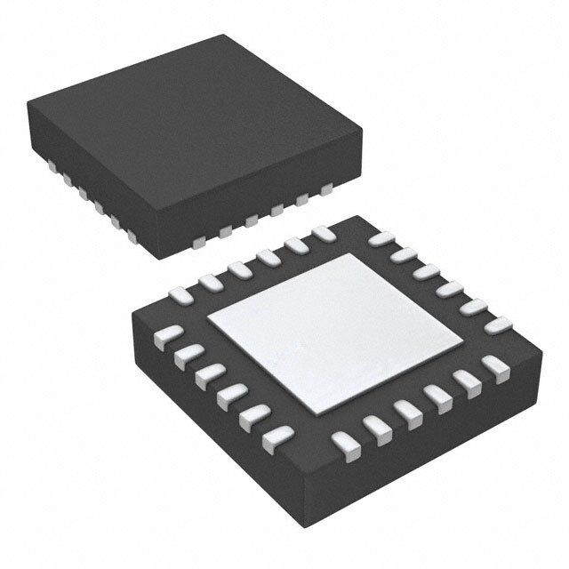
| 供应商器件封装 | 24-VQFN (4x4) |
| 其它名称 | 296-30079-6 |
| 包装 | Digi-Reel® |
| 同步整流器 | 是 |
| 商标 | Texas Instruments |
| 安装类型 | 表面贴装 |
| 安装风格 | SMD/SMT |
| 封装 | Reel |
| 封装/外壳 | 24-VFQFN 裸露焊盘 |
| 封装/箱体 | VQFN-24 |
| 工作温度 | -40°C ~ 85°C |
| 工作温度范围 | - 40 C to + 85 C |
| 工厂包装数量 | 3000 |
| 拓扑结构 | Buck (Step-Down) |
| 描述/功能 | A monolithic dual synchronous buck regulator with wide operating input voltage that can operate bus voltages and battery chemistries |
| 最大工作温度 | + 85 C |
| 最小工作温度 | - 40 C |
| 标准包装 | 1 |
| 电压-输入 | 4.5 V ~ 16 V |
| 电压-输出 | 0.8 V ~ 15 V |
| 电流-输出 | 2A,3A |
| 电源电压 | 18 V |
| 电源电流 | 1 mA |
| 类型 | 降压(降压) |
| 系列 | TPS65270 |
| 输入电压 | 18 V |
| 输出数 | 2 |
| 输出电压 | 15 V |
| 输出电流 | 3 A |
| 输出端数量 | 2 |
| 输出类型 | 可调式 |
| 配用 | /product-detail/zh/TPS65270EVM/TPS65270EVM-ND/2797922/product-detail/zh/TPS65270QEVM/TPS65270QEVM-ND/2833464 |
| 频率-开关 | 300kHz ~ 1.4MHz |


- 商务部:美国ITC正式对集成电路等产品启动337调查
- 曝三星4nm工艺存在良率问题 高通将骁龙8 Gen1或转产台积电
- 太阳诱电将投资9.5亿元在常州建新厂生产MLCC 预计2023年完工
- 英特尔发布欧洲新工厂建设计划 深化IDM 2.0 战略
- 台积电先进制程称霸业界 有大客户加持明年业绩稳了
- 达到5530亿美元!SIA预计今年全球半导体销售额将创下新高
- 英特尔拟将自动驾驶子公司Mobileye上市 估值或超500亿美元
- 三星加码芯片和SET,合并消费电子和移动部门,撤换高东真等 CEO
- 三星电子宣布重大人事变动 还合并消费电子和移动部门
- 海关总署:前11个月进口集成电路产品价值2.52万亿元 增长14.8%


PDF Datasheet 数据手册内容提取
Product Sample & Technical Tools & Support & Folder Buy Documents Software Community TPS65270 SLVSAX7E–AUGUST2011–REVISEDAUGUST2016 TPS65270 4.5-V to 18-V Input Voltage, 2-A or 3-A Output Current, Dual Synchronous Step- Down Regulator With Integrated MOSFET 1 Features 3 Description • WideInputSupplyVoltageRange:4.5Vto18V The TPS65270 is a monolithic, dual synchronous 1 buck regulator with a wide operating input voltage • 0.8V,±1%AccuracyReference that can operate in 5-V, 9-V, 12-V, or 15-V bus • Upto2-A(Buck1)and3-A(Buck2)Maximum voltages and battery chemistries. The converters are ContinuousOutputLoadingCurrent designed to simplify its application while giving the • Low-PowerPulseSkippingModetoAchieveHigh designer the option to optimize their usage according tothetargetapplication. LightLoadEfficiency • AdjustableSwitchingFrequency The TPS65270 features a precision 0.8-V reference 300kHzto1.4MHzSetbyExternalResistor and can produce output voltages up to 15 V. Each converter features an enable pin that allows • StartupWithaPrebiasedOutputVoltage dedicated control of each channel that provides • DedicatedEnableandSoftStartforEachBuck flexibility for power sequencing. Soft-start time in • PeakCurrent-ModeControlWithSimple each channel can be adjusted by choosing different CompensationCircuit external capacitors. TPS65270 is also able to start up with a prebiased output. The converter begins • Cycle-by-CycleOvercurrentProtection switching when output voltage reaches the prebiased • 180° Out-of-PhaseOperationtoReduceInput voltage. CapacitanceandPowerSupplyInducedNoise Constant frequency peak current-mode control • Availablein24-LeadThermallyEnhanced simplifies the compensation and provides fast HTSSOP(PWP)andVQFN4-mm × 4-mm(RGE) transient response. Cycle-by-cycle overcurrent Packages protection and hiccup mode operation limits MOSFET power dissipation in short-circuit or overloading fault 2 Applications conditions. Low-side reverse current protection also prevents excessive sinking current from damaging • DTV theconverter. • DSLModems • CableModems DeviceInformation(1) • Set-TopBoxes PARTNUMBER PACKAGE BODYSIZE(NOM) • CarDVDPlayers HTSSOP(24) 7.80mm×4.40mm TPS65270 • HomeGatewayandAccessPointNetworks VQFN(24) 4.00mm×4.00mm • WirelessRouters (1) For all available packages, see the orderable addendum at theendofthedatasheet. TypicalApplication EfficiencyvsOutputLoad 100 C8 ENABLE Buck1 1EN1 BST124 47nF C12059uVF 90 FB1 2FB1 VIN123 R324.b4K FB1 80 2.C23nF 1R01K 1C0n2F 34SS1 LX12212 VIN C221u0F R404.a2K C821p1F 70 COMP1 LX1 1.8V/2A (o1pC0t0i1op7nFal) C4 5LOW_P GND20 4.L71uH ncy 60 10uF 6VCC GND19 cie 50 7AGND TPS65270 GND18 Effi 40 R3 (o1pC0t0i1op6nFal) 383K 8ROSC GND17 4.L72uH 30 9 16 COMP2 LX2 1.2V/3A 20 2.C25nF 1R02K 1C0n6F 10SS2 LX215 VIN C221u4F R405.a2K C821p5F 10 VVIINN== 41.25 VV FB2 11FB2 VIN214 C13 R805.b6K FB2 0 VIN= 15 V ENABLE Buck2 12EN2 BST213 1205uVF 0 0.5 1 1.5 2 2.5 3 C12 Output Current (A) 47nF Copyright © 2016,Texas Instruments Incorporated 1 An IMPORTANT NOTICE at the end of this data sheet addresses availability, warranty, changes, use in safety-critical applications, intellectualpropertymattersandotherimportantdisclaimers.PRODUCTIONDATA.
TPS65270 SLVSAX7E–AUGUST2011–REVISEDAUGUST2016 www.ti.com Table of Contents 1 Features.................................................................. 1 8.4 DeviceFunctionalModes........................................11 2 Applications........................................................... 1 9 ApplicationandImplementation........................ 13 3 Description............................................................. 1 9.1 ApplicationInformation............................................13 4 RevisionHistory..................................................... 2 9.2 TypicalApplication..................................................13 5 Description(continued)......................................... 3 10 PowerSupplyRecommendations..................... 18 6 PinConfigurationandFunctions......................... 3 11 Layout................................................................... 18 11.1 LayoutGuidelines.................................................18 7 Specifications......................................................... 4 11.2 LayoutExample....................................................19 7.1 AbsoluteMaximumRatings......................................4 11.3 PowerDissipation.................................................19 7.2 ESDRatings..............................................................4 12 DeviceandDocumentationSupport................. 21 7.3 RecommendedOperatingConditions.......................4 7.4 ThermalInformation..................................................5 12.1 DocumentationSupport........................................21 7.5 ElectricalCharacteristics...........................................5 12.2 ReceivingNotificationofDocumentationUpdates21 7.6 TypicalCharacteristics..............................................7 12.3 CommunityResources..........................................21 12.4 Trademarks...........................................................21 8 DetailedDescription.............................................. 8 12.5 ElectrostaticDischargeCaution............................21 8.1 Overview...................................................................8 12.6 Glossary................................................................21 8.2 FunctionalBlockDiagram.........................................9 13 Mechanical,Packaging,andOrderable 8.3 FeatureDescription...................................................9 Information........................................................... 21 4 Revision History NOTE:Pagenumbersforpreviousrevisionsmaydifferfrompagenumbersinthecurrentversion. ChangesfromRevisionD(April2013)toRevisionE Page • AddedESDRatingstable,FeatureDescriptionsection,DeviceFunctionalModes,ApplicationandImplementation section,PowerSupplyRecommendationssection,Layoutsection,DeviceandDocumentationSupportsection,and Mechanical,Packaging,andOrderableInformationsection.................................................................................................. 1 • DeletedOrderingInformationtable;seePOAattheendofthedatasheet........................................................................... 1 • ChangedmaximumvalueofVoltageonVIN1,VIN2,LX1,LX2from18to20...................................................................... 4 • ChangedmaximumvalueofVoltageatLX1,LX2(maximumwithstandvoltagetransient<10ns)from18to23...............4 • ChangedmaximumvalueofOperatingvirtualjunctiontemperature,T from125to150..................................................... 4 J • ChangedAmbienttemperature(T )toJunctiontemperature(T )inRecommendedOperatingConditionstableand A J maximumvaluefrom85to125.............................................................................................................................................. 4 • UpdatedvaluesintheThermalInformationtabletoalignwithJEDECstandards................................................................. 5 • ChangedEN1andEN2pinthreshold(falling)typicalvaluetomaximumvalueinElectricalCharacteristicstable...............5 • ChangedPSMlowpowermodethreshold(falling)typicalvaluetomaximumvalueinElectricalCharacteristicstable........5 2 SubmitDocumentationFeedback Copyright©2011–2016,TexasInstrumentsIncorporated ProductFolderLinks:TPS65270
TPS65270 www.ti.com SLVSAX7E–AUGUST2011–REVISEDAUGUST2016 5 Description (continued) The switching frequency of the converters can be set from 300 KHz to 1.4 MHz with an external resistor. Two converters have 180° out-of-phase clock signals to minimize the input filter requirements and alleviate EMI and inputcapacitorrequirements. TPS65270 also features a light-load pulse skipping mode (PSM). The PSM mode allows a power loss reduction ontheinputpowersuppliedtothesystematlightloadinginordertoachievelight-loadhighefficiency. The TPS65270 is available in a 24-pin, thermally enhanced HTSSOP (PWP) package and 24-pin VQFN (RGE) package. 6 Pin Configuration and Functions PWPPackage RGEPackage 24-PinHTSSOP 24-PinVQFN TopView TopView 2 P 1 P C D _ P M S N C W M EN1 1 24 BST1 O O G C O O C R A V L C FB1 2 23 VIN1 SS1 3 22 LX1 4 3 2 1 0 9 2 2 2 2 2 1 COMP1 4 21 LX1 SS2 1 18 SS1 LOW_P 5 20 GND FB2 2 17 FB1 VCC 6 19 GND Thermal AGND 7 Pad 18 GND EN2 3 16 EN1 Thermal ROSC 8 17 GND BST2 4 Pad 15 BST1 COMP2 9 16 LX2 VIN2 5 14 VIN1 SS2 10 15 LX2 LX2 6 13 LX1 FB2 11 14 VIN2 0 1 2 7 8 9 1 1 1 EN2 12 13 BST2 Not to scale 2 D D D D 1 X N N N N X L G G G G L Not to scale PinFunctions PIN I/O DESCRIPTION NAME HTSSOP VQFN AGND 7 22 Power Analogground.ConnectallGNDpinsandpowerpadtogether. BootstrappedpowersupplytohighsidefloatinggatedriverinBuck1.Connecta47-nFceramic BST1 24 15 O capacitorfromthispintotheswitchingnodepinLX1. BootstrappedpowersupplytohighsidefloatinggatedriverinBuck2.Connecta47-nFceramic BST2 13 4 O capacitorfromthispintotheswitchingnodepinLX2. LoopcompensationpinforBuck1.ConnectaseriesRCcircuittothispintocompensatethe COMP1 4 19 O controlloopofthisconverter. LoopcompensationpinforBuck2.ConnectaseriesRCcircuittothispintocompensatethe COMP2 9 24 O controlloopofthisconverter. EnableforBuck1.LogichighenablestheBuck1;LogiclowdisablesBuck1.Ifpinisleftopena EN1 1 16 I weakinternalpulluptointernalV5Vallowsforautomaticenable;Foradelayedstart-upadda smallceramiccapacitorfromthispintoground. EnableforBuck2.LogichighenablestheBuck2.LogiclowdisablesBuck2.Ifpinisleftopena EN2 12 3 I weakinternalpulluptointernalV5Vallowsforautomaticenable;Foradelayedstart-upadda smallceramiccapacitorfromthispintoground. FeedbackvoltageforBuck1.Connectaresistordividertoset0.8Vfromtheoutputofthe FB1 2 17 I convertertoground. Copyright©2011–2016,TexasInstrumentsIncorporated SubmitDocumentationFeedback 3 ProductFolderLinks:TPS65270
TPS65270 SLVSAX7E–AUGUST2011–REVISEDAUGUST2016 www.ti.com PinFunctions(continued) PIN I/O DESCRIPTION NAME HTSSOP VQFN FeedbackvoltageforBuck2.Connectaresistordividertoset0.8Vfromtheoutputofthe FB2 11 2 I convertertoground. 17,18, 8,9,10, GND Power PowergroundforBuck1andBuck2. 19,20 11 Lowpoweroperationmode.Withactivehigh,Buck1andBuck2operateatpulseskippingmode LOW_P 5 20 I atlightload;activelowforcesbothBuck1andBuck2toPWMmode;thispincannotbeleft open. LX1 21,22 12,13 O SwitchingnodeconnectingtoinductorforBuck1. LX2 15,16 6,7 O SwitchingnodeconnectingtoinductorforBuck2. Oscillatorfrequencysetup.Connectaresistortogroundtosetthefrequencyofinternaloscillator ROSC 8 23 O clock. SoftstartinputforBuck1.Aninternal5-µAchargingcurrentissourcingtothispin.Connecta SS1 3 18 O smallceramiccapacitortothispintosettheBuck1soft-starttime. SoftstartinputforBuck2.Aninternal5-µAchargingcurrentissourcingtothispin.Connecta SS2 10 1 O smallceramiccapacitortothispintosettheBuck1soft-starttime. VCC 6 21 O Internal6.5-Vpowersupplybias.Connecta10-µFceramiccapacitorfromthispintoground. VIN1 23 14 Power InputsupplyforBuck1.Connecta10-µFceramiccapacitorclosetothispin. VIN2 14 5 Power InputsupplyforBuck2.Connecta10-µFceramiccapacitorclosetothispin. Thermal MustbesolderedtoPCBforoptimalthermalperformance.HavethermalviasonthePCBto — — — Pad enhancepowerdissipation. 7 Specifications 7.1 Absolute Maximum Ratings overoperatingfree-airtemperaturerange(unlessotherwisenoted)(1) MIN MAX UNIT VoltageatVIN1,VIN2,LX1,LX2 –0.3 20 V VoltageatLX1,LX2(maximumwithstandvoltagetransient<10ns) –1 23 V VoltageatBST1,BST2,referencedtoLX1,LX2pin –0.3 7 V VoltageatVCC,EN1,EN2,COMP1,COMP2,LOW_P –0.3 7 V VoltageatSS1,SS2,FB1,FB2,ROSC –0.3 3.6 V VoltageatAGND,GND –0.3 0.3 V Operatingvirtualjunctiontemperature,T –40 150 °C J Storagetemperature,T –55 150 °C stg (1) StressesbeyondthoselistedunderAbsoluteMaximumRatingsmaycausepermanentdamagetothedevice.Thesearestressratings only,whichdonotimplyfunctionaloperationofthedeviceattheseoranyotherconditionsbeyondthoseindicatedunderRecommended OperatingConditions.Exposuretoabsolute-maximum-ratedconditionsforextendedperiodsmayaffectdevicereliability. 7.2 ESD Ratings VALUE UNIT Human-bodymodel(HBM),perANSI/ESDA/JEDECJS-001(1) ±2000 V Electrostaticdischarge V (ESD) Charged-devicemodel(CDM),perJEDECspecificationJESD22-C101(2) ±500 (1) JEDECdocumentJEP155statesthat500-VHBMallowssafemanufacturingwithastandardESDcontrolprocess. (2) JEDECdocumentJEP157statesthat250-VCDMallowssafemanufacturingwithastandardESDcontrolprocess. 7.3 Recommended Operating Conditions overoperatingfree-airtemperaturerange(unlessotherwisenoted) MIN MAX UNIT V Inputoperatingvoltage 4.5 18 V IN T Junctiontemperature –40 125 °C J 4 SubmitDocumentationFeedback Copyright©2011–2016,TexasInstrumentsIncorporated ProductFolderLinks:TPS65270
TPS65270 www.ti.com SLVSAX7E–AUGUST2011–REVISEDAUGUST2016 7.4 Thermal Information TPS65270 THERMALMETRIC(1)(2) PWP(HTSSOP) RGE(VQFN) UNIT 24PINS 24PINS R Junction-to-ambientthermalresistance 41.3 33.8 °C/W θJA R Junction-to-case(top)thermalresistance 23.9 36.2 °C/W θJC(top) R Junction-to-boardthermalresistance 22.6 12.1 °C/W θJB ψ Junction-to-topcharacterizationparameter 0.8 0.4 °C/W JT ψ Junction-to-boardcharacterizationparameter 22.4 12.2 °C/W JB R Junction-to-case(bottom)thermalresistance 4 2.5 °C/W θJC(bot) (1) Formoreinformationabouttraditionalandnewthermalmetrics,seetheSemiconductorandICPackageThermalMetricsapplication report. (2) SeePowerPAD™ThermallyEnhancedPackage. 7.5 Electrical Characteristics T =–40°Cto125°C,V =12V,f =625kHz(unlessotherwisenoted) A IN SW PARAMETER TESTCONDITIONS MIN TYP MAX UNIT INPUTSUPPLY V InputVoltage VIN1andVIN2 4.5 18 V IN IDD Shutdown EN1=EN2=0V 10 µA SDN Nonswitchingquiescentpowersupply IDD V =V =900mV,LOW_P=high 1 mA Q_nsw current FB1 FB2 RisingV 4 4.2 4.45 IN UVLO V undervoltagelockout FallingV 3.65 3.85 4.1 V IN IN Hysteresis 0.35 V Internalbiasingsupply V loadcurrent=0A,V =12V 6.25 V CC CC IN V V LDODropoutVoltage V =5V,V loadcurrent=20mA 180 mV CC_drop CC IN CC I V currentlimit 4.5V<V <18V 200 mA VCC CC IN FEEDBACKANDERRORAMPLIFIER V =12V,V P=1.2V,T =25°C –1% 0.8 1% IN COM J V Regulatedfeedbackvoltage V FB V =12V,V =1.2V,T =–40°Cto125°C –2% 0.8 2% IN COMP J V Lineregulation:DC V =4.5Vto18V,I =1A 0.5 %/V LINEREG IN OUT V Loadregulation:DC I =10%to90%,I 0.4 %/A LOADREG OUT OUT,MAX G Erroramplifiertransconductance –2µA<I <2µA 130 µs m_EA COMP G COMPvoltagetoinductorcurrentGm ILX=0.5A 10 A/V m_SRC ENABLE,PFMMODEANDSOFTSTART Rising 1.55 V EN1andEN2pinthreshold V EN Falling 0.4 Rising 1.55 V PSMlowpowermodethreshold V PSM Falling 0.4 I SS1andSS2soft-startchargingcurrent 5 µA SS OSCILLATOR F Switchingfrequency SetbyexternalresistorROSC 0.3 1.4 MHz SW_BK ROSC=250kΩ 0.85 1 1.15 MHz F Programmablefrequency SW ROSC=500kΩ 425 500 575 kHz PROTECTION I Buck1peakinductorcurrentlimit 4.5V<V <18V 3.2 A LIMIT1 IN I Buck1lowsideMOSFETcurrentlimit 4.5V<V <18V 2 A LIMIT1_LS1 IN I Buck2peakinductorcurrentlimit 4.5V<V <18V 4.1 A LIMIT2 IN I Buck2lowsideMOSFETcurrentlimit 4.5V<V <18V 2 A LIMIT1_LS2 IN Copyright©2011–2016,TexasInstrumentsIncorporated SubmitDocumentationFeedback 5 ProductFolderLinks:TPS65270
TPS65270 SLVSAX7E–AUGUST2011–REVISEDAUGUST2016 www.ti.com Electrical Characteristics (continued) T =–40°Cto125°C,V =12V,f =625kHz(unlessotherwisenoted) A IN SW PARAMETER TESTCONDITIONS MIN TYP MAX UNIT MOSFETON-RESISTANCES R OnresistanceofhighsideFETonCH1 BST1toLX1=6.25V 120 mΩ dson_HS1 R OnresistanceoflowsideFETonCH1 V =12V 80 mΩ dson_LS1 IN R OnresistanceofhighsideFETonCH2 BST2toLX2=6.25V 95 mΩ dson_HS2 R OnresistanceoflowsideFETonCH2 V =12V 50 mΩ dson_LS2 IN T Minimumintime 80 120 ns on_min THERMALSHUTDOWN T Thermalprotectiontrippoint Risingtemperature 160 °C TRIP T Thermalprotectionhysteresis 20 °C HYST 6 SubmitDocumentationFeedback Copyright©2011–2016,TexasInstrumentsIncorporated ProductFolderLinks:TPS65270
TPS65270 www.ti.com SLVSAX7E–AUGUST2011–REVISEDAUGUST2016 7.6 Typical Characteristics T =25°C,V =12V,f =625kHz(unlessotherwisenoted) A IN SW 1.85 1.25 1.24 1.83 PWM, Vout1, Vin = 12 V 1.23 PWM, Vout2, Vin = 12 V 1.22 1.81 1.21 1.2 PSM, Vout2, Vin = 12 V PSM, Vout2, Vin = 12 V 1.79 1.19 1.18 ` 1.77 1.17 1.16 1.75 1.15 0 0.5 1 1.5 2 2.5 3 0 0.5 1 1.5 2 2.5 3 3.5 4 Buck1=1.8V 1%resistors Buck1=1.2V 1%resistors Figure1.LoadRegulation Figure2.LoadRegulation 100 95 VI= 4.5 V 90 90 80 VI=12V VI= 15 V 85 70 60 VI= 4.5 V 7850 VI= 12 V VI= 15 V 50 70 40 65 30 60 20 55 10 50 0 0 0.5 1 1.5 2 2.5 3 0 0.5 1 1.5 2 2.5 3 3.5 Buck1=3.3V Buck2=1V Figure3.Efficiency Figure4.Efficiency 100 100 Vin = 12 V Vout2 = 5 V auto PSM-PWM 90 Vin = 12 V Vout1 = 3.3 V auto PSM-PWM 90 80 80 70 70 60 60 50 50 Forced PWM Forced PWM 40 40 30 30 20 20 10 10 0 0 0 0.05 0.1 0.15 0.2 0 0.05 0.1 0.15 0.2 Buck1=3.3V Buck2=5V Figure5.Efficiency Figure6.Efficiency Copyright©2011–2016,TexasInstrumentsIncorporated SubmitDocumentationFeedback 7 ProductFolderLinks:TPS65270
TPS65270 SLVSAX7E–AUGUST2011–REVISEDAUGUST2016 www.ti.com 8 Detailed Description 8.1 Overview TPS65270 is a power management IC with two step-down buck converters. Both high-side and low-side MOSFETs are integrated to provide fully synchronous conversion with higher efficiency. TPS65270 can support 4.5-V to 18-V input supply, 2-A continuous current for Buck 1 and 3 A for Buck 2. The buck converters have an automatic PSM mode, which can improve power dissipation during light loads. Alternatively, the device implements a constant frequency mode by connecting the LOW_P pin to ground. The wide switching frequency of 300 kHz to 1.4 MHz allows for efficiency and size optimization. The switching frequency is adjustable by selecting a resistor to ground on the ROSC pin. Input ripple is reduced by 180° out-of-phase operation between Buck1andBuck2. Both buck converters have peak current mode control which simplifies the loop compensation. A traditional type II compensation network can stabilize the system and achieve fast transient response. Moreover, an optional capacitor in parallel with the upper resistor of the feedback divider provides one more zero and makes the crossover frequency over 100 kHz. Each buck converter has an individual cycle-by-cycle current limit and low sidereversecurrentlimit. The device has a built-in LDO regulator. During a standby mode, the 6.5-V LDO can be used to drive MCU and other active loads. with this LDO, system is able to turn off the two buck converters so as to reduce the power consumption and improve the standby efficiency. Each converter has its own programmable soft start that can reduce the input inrush current. The individual Enable pins for each independent control of each output voltage andpowersequence. 8 SubmitDocumentationFeedback Copyright©2011–2016,TexasInstrumentsIncorporated ProductFolderLinks:TPS65270
TPS65270 www.ti.com SLVSAX7E–AUGUST2011–REVISEDAUGUST2016 8.2 Functional Block Diagram LOW_P 5 Pre-Regulator,Voltage Reference, Logic Current Bias VCC 6 Internal 23 VIN1 VIN1 LDO ROSC 8 OSC 180o ILIM 24 BST1 SLP CS S Q 21,22 LX1 Latch VOUTBUCK1 SS1 3 COMP R Q 0.8V EA EN FB1 2 FB1 FB1 COMP1 4 19,20 GND EN1 1 EN1Logic BUCK1 12 EN2Logic EN2 17,18 9 GND COMP2 11 FB2 FB2 FB2 10 same as Buck 1 SS2 15,16 LX2 VOUTBUCK2 13 14 BST2 BUCK2 VIN2 VIN2 AGND 6 Note: Pin numbers in block diagram are for HTSSOP(PWP) 24-pin package. Copyright © 2016,Texas Instruments Incorporated 8.3 Feature Description 8.3.1 AdjustableSwitchingFrequency To select the internal switching frequency connect a resistor from ROSC to ground. Figure 7 shows the required resistanceforagivenswitchingfrequency. Copyright©2011–2016,TexasInstrumentsIncorporated SubmitDocumentationFeedback 9 ProductFolderLinks:TPS65270
TPS65270 SLVSAX7E–AUGUST2011–REVISEDAUGUST2016 www.ti.com Feature Description (continued) 900 800 700 600 W e - 500 c n a sist 400 e R 300 200 100 0 0 0.5 1 1.5 2 2.5 3 f s w - Switching Frequency - MHz Figure7. ROSCvsSwitchingFrequency R (kW)=239.13´ƒ -1.149 OSC SW (1) Foroperationat800kHz,a300-kΩ resistorisrequired. 8.3.2 Out-of-PhaseOperation To reduce input ripple current, Buck 1 and Buck 2 operate 180° out-of-phase. This enables the system having lessinputripple,thentolowercomponentcost,saveboardspaceandreduceEMI. 8.3.3 DelayedStart-Up If a delayed start-up is required on any of the buck converters fit a ceramic capacitor to the ENx pins. The delay added is approximately 0.75 ms per nF connected to the pin. The EN pins have a weak 1-MΩ pullup to the 5-V rail. 8.3.4 Soft-StartTime The device has an internal pullup current source of 5 µA that charges an external slow start capacitor to implement a slow start time. Equation 2 shows how to select a slow start capacitor based on an expected slow start time. The voltage reference (V ) is 0.8 V and the slow start charge current (I ) is 5 µA. The soft-start REF ss circuit requires 1 nF per 160 µs to be connected at the SS pin. An 800-µs soft-start time is implemented for all convertersfitting4.7nFtotherelevantpins. §C (nF)• t (ms) V (V)u¤ SS ‚ SS REF ' ISS (µA) „ (2) 8.3.5 AdjustingtheOutputVoltage The output voltage is set with a resistor divider from the output node to the FB pin. TI recommends using divider resistors of 1% tolerance or better. To improve efficiency at light load, start with 40.2 kΩ for the R1 resistor and usetheEquation3tocalculateR2. § 0.8 V • R2 R1u¤ ‚ 9 – (cid:19)(cid:17)(cid:27) 9 ' „ O (3) 10 SubmitDocumentationFeedback Copyright©2011–2016,TexasInstrumentsIncorporated ProductFolderLinks:TPS65270
TPS65270 www.ti.com SLVSAX7E–AUGUST2011–REVISEDAUGUST2016 Feature Description (continued) Vo TPS65270 R1 FB - R2 + 0.8V Figure8. VoltageDividerCircuit 8.3.6 ErrorAmplifier The device has a transconductance error amplifier. The transconductance of the error amplifier is 130 µA/V duringnormaloperation.ThefrequencycompensationnetworkisconnectedbetweentheCOMPpinandground. 8.3.7 SlopeCompensation The device has a built-in slope compensation ramp. The slope compensation can prevent subharmonic oscillationsinpeakcurrentmodecontrolwhendutycyclebecomestoolarge. 8.3.8 OvercurrentProtection Thecurrentthroughtheinternalhigh-sideMOSFETissampledandscaledthroughaninternalpilotdeviceduring the hig time. The sampled current is compared to overcurrent limit. If the peak inductor current exceeds the overcurrent limit reference level, an internal overcurrent fault counter is set to 1 and an internal flag is set. The internal power MOSFET is immediately turned off and is not turned on again until the next switching cycle. The protection circuitry continues to monitor the current and turns off the internal MOSFET as described. If the overcurrent condition persists for four sequential clock cycles, the overcurrent fault counter overflows indicating an overcurrent fault condition exists. The regulator is shut down and power good goes low. If the overcurrent condition clears before the counter reaches four consecutive cycles, the internal flag and counter are reset. The protection circuitry attempts to recover from the overcurrent condition after waiting four soft-start cycles. The internal overcurrent flag and counter are reset. A normal soft-start cycle is attempted and normal operation continues if the fault condition has cleared. If the overcurrent fault counter overflows during soft start, the convertershutsdownandthishiccupmodeoperationrepeats. 8.3.9 ThermalShutdown The device implements an internal thermal shutdown to protect itself if the junction temperature exceeds 160°C. The thermal shutdown forces the device to stop switching when the junction temperature exceeds thermal trip threshold. Once the die temperature decreases below 140°C, the device reinitiates the power up sequence. The thermalshutdownhysteresisis20°C. 8.3.10 LowPowerModeOperation By pulling the Low_P pin high all converters operate in pulse-skipping mode, greatly reducing the overall power consumption at light and no load conditions. When LOW_P is tied to low, all converters run in forced PWM mode. 8.4 Device Functional Modes 8.4.1 OperationWithMinimumV (V <4.45V) IN IN The device will operate with input voltages above the 4.45-V UVLO maximum voltage. The typical UVLO voltage is 4.2 V and the device may operate at input voltage above this point. The device may also operate with lower input voltages; the minimum UVLO voltage is 4 V (rising) and 3.65 V (falling). The device will not operate with inputvoltagesbelowtheUVLOminimumvoltage. Copyright©2011–2016,TexasInstrumentsIncorporated SubmitDocumentationFeedback 11 ProductFolderLinks:TPS65270
TPS65270 SLVSAX7E–AUGUST2011–REVISEDAUGUST2016 www.ti.com Device Functional Modes (continued) 8.4.2 OperationWithENControl The enable rising edge threshold voltage is 1.55 V (minimum) and falling edge threshold voltage is 0.4 V (maximum). With EN held below 0.4 V the device is disabled and switching is inhibited. The IC quiescent current is reduced in this state. The device becomes active when input voltage is above the UVLO threshold and the EN voltageisincreasedabove1.55V.Switchingisenabledandtheinternalsoft-startsequenceisinitiatedasshown inFigure13. 12 SubmitDocumentationFeedback Copyright©2011–2016,TexasInstrumentsIncorporated ProductFolderLinks:TPS65270
TPS65270 www.ti.com SLVSAX7E–AUGUST2011–REVISEDAUGUST2016 9 Application and Implementation NOTE Information in the following applications sections is not part of the TI component specification, and TI does not warrant its accuracy or completeness. TI’s customers are responsible for determining suitability of components for their purposes. Customers should validateandtesttheirdesignimplementationtoconfirmsystemfunctionality. 9.1 Application Information The device is a dual-synchronous, step-down DC-DC converter. It is typically used to convert a higher DC voltagetolowerDCvoltageswithcontinuousavailableoutputcurrentof2Aor3A. 9.2 Typical Application C5 R3 C3 2.2nF 383K C4 2.2nF C16 10uF C16 100pF 100pF (optional) R2 R1 (optional) 10K 10K 24 23 22 21 20 19 1C0n6F 1 COMP2 ROSC AGND VCC LOW_P COMP1 18 1C0n2F SS2 SS1 2 17 FB2 FB1 3 16 ENABLE Buck1 EN2 EN1 ENABLE Buck2 C12 TPS65270 C8 1C01u3FVIN 47nF 4 BST2 BST1 15 47nF VIN 1C0u9F 25V 25V 5 14 VIN2 VIN1 6 13 L2 LX2 LX1 L1 4.7uH 4.7uH 1.2V/3A LX2 GND GND GND GND LX1 1.8V/2A 7 8 9 10 11 12 40R.25Ka 8C21p5F C221u4F C221u0F C821p1F R404.a2K R5b R4b 80.6K 32.4K Copyright © 2016,Texas Instruments Incorporated Figure9. TypicalApplicationSchematic 9.2.1 DesignRequirements Forthisdesignexample,usetheparameterslistedinTable1astheinputparameters. Table1.DesignParameters PARAMETER EXAMPLEVALUE V 1 1.8V OUT I 1 2A OUT V 2 1.2V OUT I 2 3A OUT Transientresponse(1-Aloadstep) ±5% Inputvoltage 12V(typical),4.5Vto18V Outputvoltageripple ±1% Switchingfrequency 625kHz Copyright©2011–2016,TexasInstrumentsIncorporated SubmitDocumentationFeedback 13 ProductFolderLinks:TPS65270
TPS65270 SLVSAX7E–AUGUST2011–REVISEDAUGUST2016 www.ti.com 9.2.2 DetailedDesignProcedure 9.2.2.1 OutputInductorSelection To calculate the value of the output inductor, use Equation 4. LIR is a coefficient that represents the amount of inductor ripple current relative to the maximum output current. The inductor ripple current is filtered by the output capacitor. Therefore, choosing high inductor ripple currents impact the selection of the output capacitor since the output capacitor must have a ripple current rating equal to or greater than the inductor ripple current. In general, the inductor ripple value is at the discretion of the designer; however, LIR is normally from 0.1 to 0.3 for the majorityofapplications. V -V V L= IN max OUT ´ OUT I ´LIR V ´ƒ O IN max SW (4) For the output filter inductor, it is important that the RMS current and saturation current ratings not be exceeded. TheRMSandpeakinductorcurrentcanbefoundfromEquation6andEquation7. V -V V I = IN max OUT ´ OUT ripple L V ´ƒ IN max SW (5) æV ´(V -V )ö2 OUT IN max OUT ç ÷ ç V ´L´ƒ ÷ I = I 2+ è IN max SW ø Lrms O 12 (6) I I =I + ripple Lpeak OUT 2 (7) The current flowing through the inductor is the inductor ripple current plus the output current. During power up, faults or transient load conditions, the inductor current can increase above the calculated peak inductor current level calculated above. In transient conditions, the inductor current can increase up to the switch current limit of the device. For this reason, the most conservative approach is to specify an inductor with a saturation current ratingequaltoorgreaterthantheswitchcurrentlimitratherthanthepeakinductorcurrent. 9.2.2.2 OutputCapacitorSelection There are three primary considerations for selecting the value of the output capacitor. The output capacitor determines the modulator pole, the output voltage ripple, and how the regulator responds to a large change in loadcurrent.Theoutputcapacitanceneedstobeselectedbasedonthemoststringentofthesethreecriteria. The desired response to a large change in the load current is the first criteria. The output capacitor needs to supply the load with current when the regulator cannot. This situation would occur if there are desired hold-up times for the regulator where the output capacitor must hold the output voltage above a certain level for a specified amount of time after the input power is removed. The regulator is also temporarily not able to supply sufficient output current if there is a large, fast increase in the current needs of the load such as a transition from no load to full load. The regulator usually needs two or more clock cycles for the control loop to see the change in load current and output voltage and adjust the duty cycle to react to the change. The output capacitor must be sized to supply the extra current to the load until the control loop responds to the load change. The output capacitance must be large enough to supply the difference in current for 2 clock cycles while only allowing a tolerable amount of droop in the output voltage. Equation 8 shows the minimum output capacitance necessary to accomplishthis. 2´DI C = OUT O ƒ ´DV SW OUT where • ΔI isthechangeinoutputcurrent out • ƒ istheregulatorsswitchingfrequency sw • ΔV istheallowablechangeintheoutputvoltage. (8) out Equation9calculatestheminimumoutputcapacitanceneededtomeettheoutputvoltageripplespecification. 14 SubmitDocumentationFeedback Copyright©2011–2016,TexasInstrumentsIncorporated ProductFolderLinks:TPS65270
TPS65270 www.ti.com SLVSAX7E–AUGUST2011–REVISEDAUGUST2016 1 1 C > ´ O 8´ƒ V SW Oripple I Oripple where • ƒ istheswitchingfrequency. sw • V isthemaximumallowableoutputvoltageripple. ripple • I istheinductorripplecurrent. (9) ripple Equation 10 calculates the maximum ESR an output capacitor can have to meet the output voltage ripple specification. V R < Oripple esr I Oripple (10) Additional capacitance deratings for aging, temperature and DC bias should be factored in which increases this minimum value. Capacitors generally have limits to the amount of ripple current they can handle without failing or producing excess heat. An output capacitor that can support the inductor ripple current must be specified. Some capacitor data sheets specify the root mean square (RMS) value of the maximum ripple current. Equation 11 can beusedtocalculatetheRMSripplecurrenttheoutputcapacitorneedstosupport. V ´(V -V ) I = OUT IN max OUT Lrms 12´V ´L´ƒ IN max SW (11) 9.2.2.3 InputCapacitorSelection The TPS65265 requires a high quality ceramic, type X5R or X7R, input decoupling capacitor of at least 10 µF of effective capacitance on the PVIN input voltage pins. These capacitors must be connected as close as physically possible to the input pins of the converters. In some applications additional bulk capacitance may also be required for the PVIN input. The effective capacitance includes any DC bias effects. The voltage rating of the input capacitor must be greater than the maximum input voltage. The capacitor must also have a ripple current ratinggreaterthanthemaximuminputcurrentrippleofTheTPS65265.Theinputripplecurrentcanbecalculated usingEquation12. V (V ´V ) I =I ´ OUT ´ IN min OUT INrms OUT V V IN min IN min (12) The value of a ceramic capacitor varies significantly over temperature and the amount of DC bias applied to the capacitor. The capacitance variations due to temperature can be minimized by selecting a dielectric material that is stable over temperature. X5R and X7R ceramic dielectrics are usually selected for power regulator capacitors because they have a high capacitance to volume ratio and are fairly stable over temperature. The output capacitor must also be selected with the DC bias taken into account. The capacitance value of a capacitor decreases as the DC bias across a capacitor increases. The input capacitance value determines the input ripple voltageoftheregulator.TheinputvoltageripplecanbecalculatedusingEquation13. I ´0.25 DV = OUTmax IN C ´ƒ IN SW (13) 9.2.2.4 BootstrapCapacitorSelection The device has two integrated boot regulators and requires a small ceramic capacitor between BST and LX pins to provide the gate drive voltage for the high side MOSFET. TI recommends a ceramic capacitor of 0.047 µF. A ceramic capacitor with an X7R or X5R grade dielectric is desired because of the stable characteristics over temperatureandvoltage. 9.2.2.5 LoopCompensation TPS65270isacurrentmodecontrolDC-DCconverter.Theerroramplifierhas130-µA/Vtransconductance. Copyright©2011–2016,TexasInstrumentsIncorporated SubmitDocumentationFeedback 15 ProductFolderLinks:TPS65270
TPS65270 SLVSAX7E–AUGUST2011–REVISEDAUGUST2016 www.ti.com Vo iL Co RL Resr gm =10A/V ps Current Sense R1 Cff I/V Gain FBx Rc Vref=0.8V R2 C Cc Roll gm=130µA/V Figure10. LoopCompensation A typical compensation circuit could be type II (R and C ) to have a phase margin from 60 to 90 degrees, or C C type III (R , C and C ) to improve the converter transient response. C adds a high frequency pole to C C ff Roll attenuate high-frequency noise when required. It may also prevent noise coupling from other rails if there is possibilityofcrosscouplingbetweenrailswhenlayoutisverycompact. Tocalculatetheexternalcompensationcomponentsfollowthefollowingsteps: TYPEIICIRCUIT TYPEIIICIRCUIT Selectswitchingfrequencythatisappropriateforapplication dependingonL,Csizes,outputripple,EMIconcernsandetc. Switchingfrequenciesfrom500kHzto1MHzgivebesttradeoff UsetypeIIIcircuitforswitching — betweenperformanceandcost.WhenusingsmallerLandCs, frequencieshigherthan500kHz. switchingfrequencycanbeincreased.Tooptimizeefficiency, switchingfrequencycanbelowered. Selectcrossoverfrequency(f )tobelessthan1/5to1/10of C Suggestedf =f /10 Suggestedf =f /10 switchingfrequency. C S C S 2p´ƒ ´V ´C 2p´ƒ ´C SetandcalculateRC. RC = g ´Vcref´Ogm O RC = g ´cgm O M ps M ps CalculateC byplacingacompensationzeroatorbeforethe C converterdominantpole R ´Co R ´Co C = L C = L ƒS 1 c Rc c Rc C uR u2S O L AddC ifrequiredtoremovelargesignalcouplingtohigh Roll impedanceCOMPnode.Makesurethat Re uC Re uC ƒSRoll 2uSuR1C uCRoll CRoll sRr C O CRoll sRr C O isatleasttwicethecrossoverfrequency. CalculateC compensationzeroatlowfrequencytoboostthephase ff 1 mfreaqrguiennacytt(hfzeffcirsossmsoavlelerrftrheaqnuesnocfty.stMaratkeeqsuuivraelethnattfrtehqeuzeenrcoy(1/ — Cƒƒ (cid:21)uSuƒ]ƒƒ u5(cid:20) T ). ss 16 SubmitDocumentationFeedback Copyright©2011–2016,TexasInstrumentsIncorporated ProductFolderLinks:TPS65270
TPS65270 www.ti.com SLVSAX7E–AUGUST2011–REVISEDAUGUST2016 9.2.3 ApplicationCurves T =25°C,V =12V,f =625kHz(unlessotherwisenoted). A IN SW I =0A I =0A I =2A I =3A O1 O2 O1 O2 Figure11.Buck1andBuck2inSteadyState Figure12.Buck1andBuck2inSteadyState V =1.8V V =1.2V V =3.3V I =1Ato2A O1 O2 O1 O1 Figure13.Start-UpWithEN Figure14.Buck1LoadTransient V =1V I =1Ato2A O2 O1 Figure15.Buck2LoadTransient Figure16.Buck1andBuck2inPSMMode Copyright©2011–2016,TexasInstrumentsIncorporated SubmitDocumentationFeedback 17 ProductFolderLinks:TPS65270
TPS65270 SLVSAX7E–AUGUST2011–REVISEDAUGUST2016 www.ti.com T =25°C,V =12V,f =625kHz(unlessotherwisenoted). A IN SW Figure17.Buck2HardShortandRecover 10 Power Supply Recommendations The device is designed to operate with an input voltage supply from 4.5 V to 18 V. This input power supply must be well regulated. If the input supply is placed more than a few inches from the TPS65270 converter, bulk capacitance may be required in addition to the ceramic bypass capacitors. An electrolytic capacitor with a value of47µFisatypicalchoice. 11 Layout 11.1 Layout Guidelines LayoutisacriticalportionofPMICdesigns. • PlaceVOUT,andLXonthetoplayerandaninnerpowerplaneforVIN. • Fit also on the top layer connections for the remaining pins of the PMIC and a large top side area filled with ground. • The top layer ground area sould be connected to the bottom ground layer(s) using vias at the input bypass capacitor,theoutputfiltercpacitoranddirectlyundertheTPS65270device to provide a thermal path from the Powerpadlandtoground. • TheAGNDpinmustbetieddirectlytothepowerpadundertheICandthepowerpad. • For operation at full rated load, the top side ground area together with the bottom ground plane, must provide adequateheatdissipatingarea. • There are several signals paths that conduct fast changing currents or voltages that can interact with stray inductance or parasitic capacitance to generate noise or degrade the power supplies performance. To help eliminate these problems, the VIN pin must be bypassed to ground with a low ESR ceramic bypass capacitor with X5R or X7R dielectric. Minimize the loop area formed by the bypass capacitor connections, the VIN pins, and the ground connections. Because the LX connection is the switching node, the output inductor must be placed close to the LX pins, and the area of the PCB conductor minimized to prevent excessive capacitive coupling. • The output filter capacitor ground must use the same power ground trace as the VIN input bypass capacitor. Trytominimizethisconductorlengthwhilemaintainingadequatewidth. • The compensation must be as close as possible to the COMP pins. The COMP and OSC pins are sensitive to noise so the components associated to these pins must be placed as close as possible to the IC and routedwithminimallengthsoftrace. 18 SubmitDocumentationFeedback Copyright©2011–2016,TexasInstrumentsIncorporated ProductFolderLinks:TPS65270
TPS65270 www.ti.com SLVSAX7E–AUGUST2011–REVISEDAUGUST2016 11.2 Layout Example COMP2 ROSC AGND VCC LOW_P COMP1 SS2 SS1 FB2 FB1 EN2 EN1 VIN2 BST2 BST1 VIN1 VIN2 VIN1 LX2 LX1 X2 ND ND ND ND X1 L G G G G L VOUT2 VOUT1 0.010 in. Diameter Thermal VIAto Ground Plane VIAto Ground Plane Figure18. ExampleLayoutfortheTPS65270 11.3 Power Dissipation The total power dissipation inside TPS65270 must not exceed the maximum allowable junction temperature of 125°C to maintain reliable operation. The maximum allowable power dissipation is a function of the thermal resistanceofthepackage(R )andambienttemperature. θJA Tocalculatethetemperatureinsidethedeviceundercontinuousloadingusethefollowingprocedure. 1. Definethesetvoltageforeachconverter. 2. Definethecontinuousloadingoneachconverter.Makesuredonotexceedtheconvertermaximumloading. 3. Determine from the graphs below the expected losses in watts per converter inside the device. The losses dependontheinputsupply,theselectedswitchingfrequency,theoutputvoltageandtheconverterchosen. Copyright©2011–2016,TexasInstrumentsIncorporated SubmitDocumentationFeedback 19 ProductFolderLinks:TPS65270
TPS65270 SLVSAX7E–AUGUST2011–REVISEDAUGUST2016 www.ti.com Power Dissipation (continued) 4. TocalculatethemaximumtemperatureinsidetheICusethefollowingformula: T =T +P ´R HOT_SPOT A DIS qJA where • P isthesumoflossesinallconverters DIS • R isthejunctiontoambientthermalimpedanceofthedeviceanditisheavilydependantonboardlayout θJA (14) 1.7 1.7 1.6 1.6 1.5 1.5 1.4 1.4 1.3 1.3 1.2 1.2 1.1 1.1 1.0 1.0 0.9 0.9 0.8 0.8 0.7 0.7 0.6 0.6 0.5 0.5 0.4 0.4 0.3 0.3 0.2 0.2 1 1.2 1.4 1.6 1.8 2 2.2 2.4 2.6 2.8 3 1 1.2 1.4 1.6 1.8 2 2.2 2.4 2.6 2.8 3 I (A) I (A) V =12V f =500kHz V =12V f =1.1MHz IN SW IN SW V (fromtoptobottom)=5V,3.3V,2.5V,1.8V,1.2V V (fromtoptobottom)=5V,3.3V,2.5V,1.8V,1.2V OUT OUT Figure19.Buck1 Figure20.Buck1 1.6 1.6 1.4 1.4 1.2 1.2 1.0 1.0 0.8 0.8 0.6 0.6 0.4 0.4 0.2 0.2 1 1.2 1.4 1.6 1.8 2 2.2 2.4 2.6 2.8 3 3.2 3.4 3.6 1 1.2 1.4 1.6 1.8 2 2.2 2.4 2.6 2.8 3 3.2 3.4 3.6 I (A) I (A) VIN=12V fSW=500kHz VIN=12V fSW=1.1MHz VOUT(fromtoptobottom)=5V,3.3V,2.5V,1.8V,1.2V VOUT(fromtoptobottom)=5V,3.3V,2.5V,1.8V,1.2V Figure21.Buck2 Figure22.Buck2 20 SubmitDocumentationFeedback Copyright©2011–2016,TexasInstrumentsIncorporated ProductFolderLinks:TPS65270
TPS65270 www.ti.com SLVSAX7E–AUGUST2011–REVISEDAUGUST2016 12 Device and Documentation Support 12.1 Documentation Support 12.1.1 RelatedDocumentation Forrelateddocumentationseethefollowing: PowerPAD™ThermallyEnhancedPackage(SLMA002) 12.2 Receiving Notification of Documentation Updates To receive notification of documentation updates, navigate to the device product folder on ti.com. In the upper right corner, click on Alert me to register and receive a weekly digest of any product information that has changed.Forchangedetails,reviewtherevisionhistoryincludedinanyreviseddocument. 12.3 Community Resources The following links connect to TI community resources. Linked contents are provided "AS IS" by the respective contributors. They do not constitute TI specifications and do not necessarily reflect TI's views; see TI's Terms of Use. TIE2E™OnlineCommunity TI'sEngineer-to-Engineer(E2E)Community.Createdtofostercollaboration amongengineers.Ate2e.ti.com,youcanaskquestions,shareknowledge,exploreideasandhelp solveproblemswithfellowengineers. DesignSupport TI'sDesignSupport QuicklyfindhelpfulE2Eforumsalongwithdesignsupporttoolsand contactinformationfortechnicalsupport. 12.4 Trademarks PowerPAD,E2EaretrademarksofTexasInstruments. Allothertrademarksarethepropertyoftheirrespectiveowners. 12.5 Electrostatic Discharge Caution This integrated circuit can be damaged by ESD. Texas Instruments recommends that all integrated circuits be handled with appropriateprecautions.Failuretoobserveproperhandlingandinstallationprocedurescancausedamage. ESDdamagecanrangefromsubtleperformancedegradationtocompletedevicefailure.Precisionintegratedcircuitsmaybemore susceptibletodamagebecauseverysmallparametricchangescouldcausethedevicenottomeetitspublishedspecifications. 12.6 Glossary SLYZ022—TIGlossary. Thisglossarylistsandexplainsterms,acronyms,anddefinitions. 13 Mechanical, Packaging, and Orderable Information The following pages include mechanical, packaging, and orderable information. This information is the most current data available for the designated devices. This data is subject to change without notice and revision of thisdocument.Forbrowser-basedversionsofthisdatasheet,refertotheleft-handnavigation. Copyright©2011–2016,TexasInstrumentsIncorporated SubmitDocumentationFeedback 21 ProductFolderLinks:TPS65270
PACKAGE OPTION ADDENDUM www.ti.com 6-Feb-2020 PACKAGING INFORMATION Orderable Device Status Package Type Package Pins Package Eco Plan Lead/Ball Finish MSL Peak Temp Op Temp (°C) Device Marking Samples (1) Drawing Qty (2) (6) (3) (4/5) TPS65270PWPR ACTIVE HTSSOP PWP 24 2000 Green (RoHS NIPDAU Level-2-260C-1 YEAR -40 to 85 TPS65270 & no Sb/Br) TPS65270RGER ACTIVE VQFN RGE 24 3000 Green (RoHS NIPDAU Level-2-260C-1 YEAR -40 to 85 TPS & no Sb/Br) 65270 TPS65270RGET ACTIVE VQFN RGE 24 250 Green (RoHS NIPDAU Level-2-260C-1 YEAR -40 to 85 TPS & no Sb/Br) 65270 (1) The marketing status values are defined as follows: ACTIVE: Product device recommended for new designs. LIFEBUY: TI has announced that the device will be discontinued, and a lifetime-buy period is in effect. NRND: Not recommended for new designs. Device is in production to support existing customers, but TI does not recommend using this part in a new design. PREVIEW: Device has been announced but is not in production. Samples may or may not be available. OBSOLETE: TI has discontinued the production of the device. (2) RoHS: TI defines "RoHS" to mean semiconductor products that are compliant with the current EU RoHS requirements for all 10 RoHS substances, including the requirement that RoHS substance do not exceed 0.1% by weight in homogeneous materials. Where designed to be soldered at high temperatures, "RoHS" products are suitable for use in specified lead-free processes. TI may reference these types of products as "Pb-Free". RoHS Exempt: TI defines "RoHS Exempt" to mean products that contain lead but are compliant with EU RoHS pursuant to a specific EU RoHS exemption. Green: TI defines "Green" to mean the content of Chlorine (Cl) and Bromine (Br) based flame retardants meet JS709B low halogen requirements of <=1000ppm threshold. Antimony trioxide based flame retardants must also meet the <=1000ppm threshold requirement. (3) MSL, Peak Temp. - The Moisture Sensitivity Level rating according to the JEDEC industry standard classifications, and peak solder temperature. (4) There may be additional marking, which relates to the logo, the lot trace code information, or the environmental category on the device. (5) Multiple Device Markings will be inside parentheses. Only one Device Marking contained in parentheses and separated by a "~" will appear on a device. If a line is indented then it is a continuation of the previous line and the two combined represent the entire Device Marking for that device. (6) Lead/Ball Finish - Orderable Devices may have multiple material finish options. Finish options are separated by a vertical ruled line. Lead/Ball Finish values may wrap to two lines if the finish value exceeds the maximum column width. Important Information and Disclaimer:The information provided on this page represents TI's knowledge and belief as of the date that it is provided. TI bases its knowledge and belief on information provided by third parties, and makes no representation or warranty as to the accuracy of such information. Efforts are underway to better integrate information from third parties. TI has taken and continues to take reasonable steps to provide representative and accurate information but may not have conducted destructive testing or chemical analysis on incoming materials and chemicals. TI and TI suppliers consider certain information to be proprietary, and thus CAS numbers and other limited information may not be available for release. Addendum-Page 1
PACKAGE OPTION ADDENDUM www.ti.com 6-Feb-2020 In no event shall TI's liability arising out of such information exceed the total purchase price of the TI part(s) at issue in this document sold by TI to Customer on an annual basis. Addendum-Page 2
PACKAGE MATERIALS INFORMATION www.ti.com 13-May-2013 TAPE AND REEL INFORMATION *Alldimensionsarenominal Device Package Package Pins SPQ Reel Reel A0 B0 K0 P1 W Pin1 Type Drawing Diameter Width (mm) (mm) (mm) (mm) (mm) Quadrant (mm) W1(mm) TPS65270PWPR HTSSOP PWP 24 2000 330.0 16.4 6.95 8.3 1.6 8.0 16.0 Q1 TPS65270RGER VQFN RGE 24 3000 330.0 12.4 4.25 4.25 1.15 8.0 12.0 Q2 TPS65270RGET VQFN RGE 24 250 180.0 12.4 4.25 4.25 1.15 8.0 12.0 Q2 PackMaterials-Page1
PACKAGE MATERIALS INFORMATION www.ti.com 13-May-2013 *Alldimensionsarenominal Device PackageType PackageDrawing Pins SPQ Length(mm) Width(mm) Height(mm) TPS65270PWPR HTSSOP PWP 24 2000 367.0 367.0 38.0 TPS65270RGER VQFN RGE 24 3000 367.0 367.0 35.0 TPS65270RGET VQFN RGE 24 250 210.0 185.0 35.0 PackMaterials-Page2
GENERIC PACKAGE VIEW PWP 24 PowerPADTM TSSOP - 1.2 mm max height 4.4 x 7.6, 0.65 mm pitch PLASTIC SMALL OUTLINE This image is a representation of the package family, actual package may vary. Refer to the product data sheet for package details. 4224742/B www.ti.com
PACKAGE OUTLINE PWP0024P PowerPAD TM TSSOP - 1.2 mm max height SCALE 2.000 SMALL OUTLINE PACKAGE 6.6 C TYP 6.2 A 0.1 C PIN 1 INDEX SEATING AREA 22X 0.65 PLANE 24 1 2X 7.9 7.15 7.7 NOTE 3 12 13 0.30 4.5 24X B 0.19 4.3 0.1 C A B SEE DETAIL A (0.15) TYP 2X 1.00 MAX NOTE 5 12 13 2X 0.35 MAX NOTE 5 0.25 GAGE PLANE 1.2 MAX 2.98 25 2.08 THERMAL PAD 0.75 0.15 0 -8 0.50 0.05 DETA 20AIL A 1 24 TYPICAL 2.4 1.5 4224478/A 10/2018 PowerPAD is a trademark of Texas Instruments. NOTES: 1. All linear dimensions are in millimeters. Any dimensions in parenthesis are for reference only. Dimensioning and tolerancing per ASME Y14.5M. 2. This drawing is subject to change without notice. 3. This dimension does not include mold flash, protrusions, or gate burrs. Mold flash, protrusions, or gate burrs shall not exceed 0.15 mm per side. 4. Reference JEDEC registration MO-153. 5. Features may differ or may not be present. www.ti.com
EXAMPLE BOARD LAYOUT PWP0024P PowerPAD TM TSSOP - 1.2 mm max height SMALL OUTLINE PACKAGE (3.4) NOTE 9 (2.4) METAL COVERED SYMM 24X (1.5) BY SOLDER MASK 1 24X (0.45) 24 SEE DETAILS (R0.05) TYP 22X (0.65) (2.98) SYMM 25 (7.8) (1) TYP NOTE 9 SOLDER MASK DEFINED PAD ( 0.2) TYP VIA 12 13 (1) TYP (5.8) LAND PATTERN EXAMPLE EXPOSED METAL SHOWN SCALE: 8X SOLDER MASK METAL METAL UNDER SOLDER MASK OPENING SOLDER MASK OPENING EXPOSED METAL EXPOSED METAL 0.05 MAX 0.05 MIN ALL AROUND ALL AROUND NON-SOLDER MASK SOLDER MASK DEFINED DEFINED SOLDE15.000R MASK DETAILS 4224478/A 10/2018 NOTES: (continued) 6. Publication IPC-7351 may have alternate designs. 7. Solder mask tolerances between and around signal pads can vary based on board fabrication site. 8. This package is designed to be soldered to a thermal pad on the board. For more information, see Texas Instruments literature numbers SLMA002 (www.ti.com/lit/slma002) and SLMA004 (www.ti.com/lit/slma004). 9. Size of metal pad may vary due to creepage requirement. 10. Vias are optional depending on application, refer to device data sheet. It is recommended that vias under paste be filled, plugged or tented. www.ti.com
EXAMPLE STENCIL DESIGN PWP0024P PowerPAD TM TSSOP - 1.2 mm max height SMALL OUTLINE PACKAGE (2.4) BASED ON METAL COVERED 0.125 THICK 24X (1.5) BY SOLDER MASK STENCIL 1 24X (0.45) 24 (R0.05) TYP 22X (0.65) SYMM 25 (2.98) BASED ON 0.125 THICK STENCIL 12 13 SYMM SEE TABLE FOR DIFFERENT OPENINGS FOR OTHER STENCIL (5.8) THICKNESSES SOLDER PASTE EXAMPLE BASED ON 0.125 mm THICK STENCIL SCALE: 8X STENCIL SOLDER STENCIL THICKNESS OPENING 0.1 2.68 X 3.33 0.125 2.40 X 2.98 (SHOWN) 0.15 2.19 X 2.72 0.175 2.03 X 2.52 4224478/A 10/2018 NOTES: (continued) 11. Laser cutting apertures with trapezoidal walls and rounded corners may offer better paste release. IPC-7525 may have alternate design recommendations. 12. Board assembly site may have different recommendations for stencil design. www.ti.com
GENERIC PACKAGE VIEW RGE 24 VQFN - 1 mm max height PLASTIC QUAD FLATPACK - NO LEAD Images above are just a representation of the package family, actual package may vary. Refer to the product data sheet for package details. 4204104/H
PACKAGE OUTLINE RGE0024B VQFN - 1 mm max height SCALE 3.000 PLASTIC QUAD FLATPACK - NO LEAD A 4.1 B 3.9 0.5 0.3 PIN 1 INDEX AREA 4.1 3.9 0.3 0.2 DETAIL OPTIONAL TERMINAL TYPICAL C 1 MAX SEATING PLANE 0.05 0.00 0.08 C 2X 2.5 2.45 0.1 (0.2) TYP 7 12 EXPOSED SEE TERMINAL THERMAL PAD DETAIL 6 13 2X 25 SYMM 2.5 1 18 0.3 20X 0.5 24X 0.2 24 SYMM 19 0.1 C A B PIN 1 ID 0.05 (OPTIONAL) 0.5 24X 0.3 4219013/A 05/2017 NOTES: 1. All linear dimensions are in millimeters. Any dimensions in parenthesis are for reference only. Dimensioning and tolerancing per ASME Y14.5M. 2. This drawing is subject to change without notice. 3. The package thermal pad must be soldered to the printed circuit board for thermal and mechanical performance. www.ti.com
EXAMPLE BOARD LAYOUT RGE0024B VQFN - 1 mm max height PLASTIC QUAD FLATPACK - NO LEAD ( 2.45) SYMM 24 19 24X (0.6) 1 18 24X (0.25) (R0.05) TYP 25 SYMM (3.8) 20X (0.5) 13 6 ( 0.2) TYP VIA 7 12 (0.975) TYP (3.8) LAND PATTERN EXAMPLE EXPOSED METAL SHOWN SCALE:15X 0.07 MAX 0.07 MIN ALL AROUND ALL AROUND SOLDER MASK METAL OPENING EXPMOESTEADL SOOPLEDNEINRG MASK EXPMOESTEADL MSOELTDAEL RU NMDAESRK NON SOLDER MASK SOLDER MASK DEFINED DEFINED (PREFERRED) SOLDER MASK DETAILS 4219013/A 05/2017 NOTES: (continued) 4. This package is designed to be soldered to a thermal pad on the board. For more information, see Texas Instruments literature number SLUA271 (www.ti.com/lit/slua271). 5. Vias are optional depending on application, refer to device data sheet. If any vias are implemented, refer to their locations shown on this view. It is recommended that vias under paste be filled, plugged or tented. www.ti.com
EXAMPLE STENCIL DESIGN RGE0024B VQFN - 1 mm max height PLASTIC QUAD FLATPACK - NO LEAD 4X ( 1.08) (0.64) TYP 24 19 24X (0.6) 1 25 18 24X (0.25) (R0.05) TYP (0.64) TYP SYMM (3.8) 20X (0.5) 13 6 METAL TYP 7 12 SYMM (3.8) SOLDER PASTE EXAMPLE BASED ON 0.125 mm THICK STENCIL EXPOSED PAD 25 78% PRINTED SOLDER COVERAGE BY AREA UNDER PACKAGE SCALE:20X 4219013/A 05/2017 NOTES: (continued) 6. Laser cutting apertures with trapezoidal walls and rounded corners may offer better paste release. IPC-7525 may have alternate design recommendations. www.ti.com
IMPORTANTNOTICEANDDISCLAIMER TI PROVIDES TECHNICAL AND RELIABILITY DATA (INCLUDING DATASHEETS), DESIGN RESOURCES (INCLUDING REFERENCE DESIGNS), APPLICATION OR OTHER DESIGN ADVICE, WEB TOOLS, SAFETY INFORMATION, AND OTHER RESOURCES “AS IS” AND WITH ALL FAULTS, AND DISCLAIMS ALL WARRANTIES, EXPRESS AND IMPLIED, INCLUDING WITHOUT LIMITATION ANY IMPLIED WARRANTIES OF MERCHANTABILITY, FITNESS FOR A PARTICULAR PURPOSE OR NON-INFRINGEMENT OF THIRD PARTY INTELLECTUAL PROPERTY RIGHTS. These resources are intended for skilled developers designing with TI products. You are solely responsible for (1) selecting the appropriate TI products for your application, (2) designing, validating and testing your application, and (3) ensuring your application meets applicable standards, and any other safety, security, or other requirements. These resources are subject to change without notice. TI grants you permission to use these resources only for development of an application that uses the TI products described in the resource. Other reproduction and display of these resources is prohibited. No license is granted to any other TI intellectual property right or to any third party intellectual property right. TI disclaims responsibility for, and you will fully indemnify TI and its representatives against, any claims, damages, costs, losses, and liabilities arising out of your use of these resources. TI’s products are provided subject to TI’s Terms of Sale (www.ti.com/legal/termsofsale.html) or other applicable terms available either on ti.com or provided in conjunction with such TI products. TI’s provision of these resources does not expand or otherwise alter TI’s applicable warranties or warranty disclaimers for TI products. Mailing Address: Texas Instruments, Post Office Box 655303, Dallas, Texas 75265 Copyright © 2020, Texas Instruments Incorporated