ICGOO在线商城 > 集成电路(IC) > PMIC - 稳压器 - DC DC 开关稳压器 > TPS62110RSAR
 Datasheet下载
- 型号: TPS62110RSAR
- 制造商: Texas Instruments
- 库位|库存: xxxx|xxxx
- 要求:
| 数量阶梯 | 香港交货 | 国内含税 |
| +xxxx | $xxxx | ¥xxxx |
查看当月历史价格
查看今年历史价格
TPS62110RSAR产品简介:
ICGOO电子元器件商城为您提供TPS62110RSAR由Texas Instruments设计生产,在icgoo商城现货销售,并且可以通过原厂、代理商等渠道进行代购。 TPS62110RSAR价格参考¥询价-¥询价。Texas InstrumentsTPS62110RSAR封装/规格:PMIC - 稳压器 - DC DC 开关稳压器, 可调式 降压 开关稳压器 IC 正 1.2V 1 输出 1.5A 16-VQFN 裸露焊盘。您可以下载TPS62110RSAR参考资料、Datasheet数据手册功能说明书,资料中有TPS62110RSAR 详细功能的应用电路图电压和使用方法及教程。
TPS62110RSAR是德州仪器(Texas Instruments, TI)推出的一款高效同步降压DC-DC开关稳压器,主要应用于需要高效率、低功耗和小尺寸解决方案的场景。以下是该型号的一些典型应用场景:

 1. 便携式电子设备
TPS62110RSAR广泛应用于便携式电子设备中,如智能手机、平板电脑、可穿戴设备等。这些设备对电源管理要求极高,尤其是电池续航能力。TPS62110RSAR通过其高效的转换效率(高达95%),能够显著延长电池寿命,同时其紧凑的封装设计也节省了宝贵的电路板空间。

 2. 物联网(IoT)设备
在物联网设备中,TPS62110RSAR可以为各种传感器、微控制器和其他低功耗组件提供稳定的电源。由于物联网设备通常依赖电池供电,且需要长时间运行,因此高效的电源管理至关重要。TPS62110RSAR的低静态电流(Iq)特性使其非常适合这类应用,能够在不影响性能的前提下最大限度地减少功耗。

 3. 工业自动化与控制
在工业自动化领域,TPS62110RSAR可用于为各种嵌入式系统、PLC(可编程逻辑控制器)、传感器节点等提供电源。它能够处理较大的负载变化,并保持输出电压的稳定性,确保系统的可靠性和稳定性。此外,其宽输入电压范围(2.5V至5.5V)使得它可以适应多种不同的电源输入条件。

 4. 医疗设备
在医疗设备中,电源的稳定性和可靠性尤为重要。TPS62110RSAR可以为便携式医疗设备(如血糖仪、心率监测器等)提供稳定的电源供应,确保设备在使用过程中不会因为电源波动而出现误判或故障。其小巧的尺寸和高效的性能也使得它非常适合用于空间有限的医疗设备中。

 5. 通信设备
在通信设备中,TPS62110RSAR可以为射频模块、基带处理器等关键组件提供稳定的电源。它的快速瞬态响应能力能够应对通信设备中频繁的负载变化,确保信号传输的稳定性和可靠性。此外,其低噪声特性也有助于减少对敏感通信电路的干扰。

综上所述,TPS62110RSAR凭借其高效、低功耗、小尺寸等优势,适用于多种对电源管理有严格要求的应用场景,特别是在便携式电子设备、物联网、工业自动化、医疗设备和通信设备等领域表现尤为突出。
| 参数 | 数值 |
| 产品目录 | 集成电路 (IC)半导体 |
| 描述 | IC REG BUCK SYNC ADJ 1.5A 16QFN稳压器—开关式稳压器 Adj 1.5-A 17-V Vin Step-Down Converter |
| 产品分类 | |
| 品牌 | Texas Instruments |
| 产品手册 | http://www.ti.com/lit/gpn/tps62110 |
| 产品图片 |
|
| rohs | 符合RoHS无铅 / 符合限制有害物质指令(RoHS)规范要求 |
| 产品系列 | 电源管理 IC,稳压器—开关式稳压器,Texas Instruments TPS62110RSAR- |
| 数据手册 | |
| 产品型号 | TPS62110RSAR |
| PWM类型 | 电压模式 |
| 产品目录页面 | |
| 产品种类 | 稳压器—开关式稳压器 |
| 供应商器件封装 | 16-QFN(4x4) |
| 其它名称 | 296-24839-1 |
| 制造商产品页 | http://www.ti.com/general/docs/suppproductinfo.tsp?distId=10&orderablePartNumber=TPS62110RSAR |
| 包装 | 剪切带 (CT) |
| 单位重量 | 46 mg |
| 参考设计库 | http://www.digikey.com/rdl/4294959904/4294959903/330 |
| 同步整流器 | 是 |
| 商标 | Texas Instruments |
| 安装类型 | 表面贴装 |
| 安装风格 | SMD/SMT |
| 封装 | Reel |
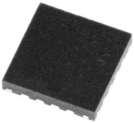
| 封装/外壳 | 16-VQFN 裸露焊盘 |
| 封装/箱体 | VQFN-16 |
| 工作温度 | -40°C ~ 85°C |
| 工作温度范围 | - 40 C to + 85 C |
| 工厂包装数量 | 3000 |
| 开关频率 | 1 MHz |
| 拓扑结构 | Buck |
| 最大工作温度 | + 85 C |
| 最大输入电压 | 17 V |
| 最小工作温度 | - 40 C |
| 最小输入电压 | 3.1 V |
| 标准包装 | 1 |
| 电压-输入 | 3.1 V ~ 17 V |
| 电压-输出 | 1.2 V ~ 16 V |
| 电流-输出 | 1.5A |
| 类型 | 降压(降压) |
| 系列 | TPS62110 |
| 输入电压 | 3.1 V to 17 V |
| 输出数 | 1 |
| 输出电压 | 1.2 V to 16 V |
| 输出电流 | 1.5 A |
| 输出端数量 | 1 Output |
| 输出类型 | 可调式 |
| 配用 | /product-detail/zh/TPS62110EVM-101/296-21163-ND/1216769/product-detail/zh/TPS62110EVM-346/296-31247-ND/2048004 |
| 频率-开关 | 1MHz |


- 商务部:美国ITC正式对集成电路等产品启动337调查
- 曝三星4nm工艺存在良率问题 高通将骁龙8 Gen1或转产台积电
- 太阳诱电将投资9.5亿元在常州建新厂生产MLCC 预计2023年完工
- 英特尔发布欧洲新工厂建设计划 深化IDM 2.0 战略
- 台积电先进制程称霸业界 有大客户加持明年业绩稳了
- 达到5530亿美元!SIA预计今年全球半导体销售额将创下新高
- 英特尔拟将自动驾驶子公司Mobileye上市 估值或超500亿美元
- 三星加码芯片和SET,合并消费电子和移动部门,撤换高东真等 CEO
- 三星电子宣布重大人事变动 还合并消费电子和移动部门
- 海关总署:前11个月进口集成电路产品价值2.52万亿元 增长14.8%


PDF Datasheet 数据手册内容提取
Product Sample & Technical Tools & Support & Folder Buy Documents Software Community TPS62110,TPS62111,TPS62112,TPS62113 SLVS585E–JULY2005–REVISEDJUNE2015 TPS6211x 17-V, 1.5-A, Synchronous Step-Down Converter 1 Features 3 Description • High-EfficiencySynchronousStep-Down The TPS6211x devices are a family of low-noise 1 synchronous step-down DC-DC converters that are ConverterWithupto95%Efficiency ideally suited for systems powered from a 2- to 4-cell • 3.1-Vto17-VOperatingInputVoltageRange Li-ionbatteryorfroma12-Vor15-Vrail. • AdjustableOutputVoltageRange:1.2Vto16V The TPS6211x devices are synchronous pulse width • FixedOutputVoltageOptionsAvailablein modulation (PWM) converters with integrated N- and 3.3Vand5V P-channel power MOSFET switches. Synchronous • SynchronizabletoExternalClock:Upto1.4MHz rectification is used to increase efficiency and to reduce external component count. To achieve highest • Upto1.5-AOutputCurrent efficiency over a wide load-current range, the • HighEfficiencyOveraWideLoad-Current converter enters a power-saving, pulse frequency RangeDuetoPFM/PWMOperationMode modulation (PFM) mode at light load currents. • 100%MaximumDutyCycleforLowestDropout Operating frequency is typically 1 MHz, allowing the use of small inductor and capacitor values. The • 20-µAQuiescentCurrent(Typical) device can be synchronized to an external clock • OvertemperatureandOvercurrentProtected signal in the range of 0.8 MHz to 1.4 MHz. For low- • Availablein16-PinVQFNPackage noise operation, the converter can be operated in PWM-only mode. In shutdown mode, the current 2 Applications consumption is reduced to less than 2 µA. The TPS6211x family of devices are available in the 16- • Point-of-LoadRegulationFrom12-VBuses pin (RSA) VQFN package, and operate over a free- • Organizers,PDAs,andHandheldPCs airtemperaturerangeof–40°Cto85°C. • HandheldScanners DeviceInformation(1) PARTNUMBER PACKAGE BODYSIZE(NOM) TPS62110 TPS62111 VQFN(16) 4.00mm×4.00mm TPS62112 TPS62113 (1) For all available packages, see the orderable addendum at theendofthedatasheet. 4 Typical Application Schematic VI= 3.8 V to 17 V TPS62111 6.8mH TPS62111 VIN SW VO= 3.3 V Efficiency vs Output Current VIN SW EN 1 MW 100 4.2 V VINA PG 90 CI=2 51 0VmF 1mF AGND LBO CO6=. 32 2VmF 80 LBI FB 70 5 V % SYNC y - 60 8.4 V c n GND GND PwPDPGNDPGND cie 50 Effi 40 12 V 30 20 VO= 3.3 V TA= 25oC 10 PFM Mode 0 0.0001 0.001 0.01 0.1 1 10 IO- Output Current-A 1 An IMPORTANT NOTICE at the end of this data sheet addresses availability, warranty, changes, use in safety-critical applications, intellectualpropertymattersandotherimportantdisclaimers.PRODUCTIONDATA.
TPS62110,TPS62111,TPS62112,TPS62113 SLVS585E–JULY2005–REVISEDJUNE2015 www.ti.com Table of Contents 1 Features.................................................................. 1 9.4 DeviceFunctionalModes........................................12 2 Applications........................................................... 1 10 ApplicationandImplementation........................ 15 3 Description............................................................. 1 10.1 ApplicationInformation..........................................15 4 TypicalApplicationSchematic............................. 1 10.2 TypicalApplications..............................................15 10.3 SystemExamples.................................................22 5 RevisionHistory..................................................... 2 11 PowerSupplyRecommendations..................... 23 6 DeviceComparisonTable..................................... 4 12 Layout................................................................... 23 7 PinConfigurationandFunctions......................... 4 12.1 LayoutGuidelines.................................................23 8 Specifications......................................................... 5 12.2 LayoutExample....................................................24 8.1 AbsoluteMaximumRatings .....................................5 13 DeviceandDocumentationSupport................. 25 8.2 ESDRatings..............................................................5 13.1 DeviceSupport......................................................25 8.3 RecommendedOperatingConditions.......................5 13.2 RelatedLinks........................................................25 8.4 ThermalInformation..................................................5 13.3 CommunityResources..........................................25 8.5 ElectricalCharacteristics...........................................6 13.4 Trademarks...........................................................25 8.6 TypicalCharacteristics..............................................8 13.5 ElectrostaticDischargeCaution............................25 9 DetailedDescription.............................................. 9 13.6 Glossary................................................................25 9.1 Overview...................................................................9 14 Mechanical,Packaging,andOrderable 9.2 FunctionalBlockDiagram.......................................10 Information........................................................... 25 9.3 FeatureDescription.................................................10 5 Revision History NOTE:Pagenumbersforpreviousrevisionsmaydifferfrompagenumbersinthecurrentversion. ChangesfromRevisionD(January2014)toRevisionE Page • AddedPinConfigurationandFunctionssection,ESDRatingstable,FeatureDescriptionsection,DeviceFunctional Modes,ApplicationandImplementationsection,PowerSupplyRecommendationssection,Layoutsection,Device andDocumentationSupportsection,andMechanical,Packaging,andOrderableInformationsection .............................. 1 ChangesfromRevisionC(October2012)toRevisionD Page • ChangedtheFUNCTIONALBLOCKDIAGRAMtoincludetheSYNCpin.......................................................................... 10 • ChangedtheRevisionHistorylist......................................................................................................................................... 22 ChangesfromRevisionB(October2012)toRevisionC Page • ChangedESD-HBMFrom:4kVTo:2kV............................................................................................................................ 5 • DeletedESD-MM.................................................................................................................................................................. 5 • ChangedESD-CDMFrom:1.5kVTo:500V....................................................................................................................... 5 • ChangedtheCONSTANT-FREQUENCYMODEOFOPERATION(SYNC=HIGH)section............................................. 13 ChangesfromRevisionA(February2009)toRevisionB Page • ChangedDescriptiontextFrom:2-cellLi-ionbatteryTo:2to4-cellLi-ionbattery................................................................ 1 • AddedtexttotheTerminalFunctionsENpindescription-Donotleavefloating.................................................................. 4 • AddedESDinformationtotheABSOLUTEMAXIMUMRATINGStable............................................................................... 5 • ChangedFrom:DissipationRatingstableTo:ThermalInformationtable............................................................................. 5 • AddedTPS62113totheOUTPUTsectionoftheElectricalCharacteristics.......................................................................... 7 • ChangedNoteAoftheFunctionalBlockDiagram............................................................................................................... 10 • ChangedtheENABLEsection............................................................................................................................................. 10 • ChangedtheLOW-BATTERYDETECTOR(StandardVersion)section............................................................................. 11 2 SubmitDocumentationFeedback Copyright©2005–2015,TexasInstrumentsIncorporated ProductFolderLinks:TPS62110 TPS62111 TPS62112 TPS62113
TPS62110,TPS62111,TPS62112,TPS62113 www.ti.com SLVS585E–JULY2005–REVISEDJUNE2015 • DeletedthePwPDpinfromFigure4, .................................................................................................................................. 11 • ChangedtheENABLE/Low-BatteryDetector(EnhancedVersion)TPS62113Onlysection............................................... 11 • ChangedthePOWER-GOODCOMPARATORsection....................................................................................................... 11 • AddedtheTHERMALSHUTDOWNsection........................................................................................................................ 12 • ChangedtheSOFTSTARTsection..................................................................................................................................... 12 • Deleted"bypullingtheSYNCpinLOW."-CONSTANT-FREQUENCYMODEOFOPERATION(SYNC=HIGH)........... 13 • Changed .............................................................................................................................................................................. 13 • ChangedPwPDtoETPadinFigure6toFigure21............................................................................................................. 15 • ChangedtheINPUT-CAPACITORSELECTIONsection..................................................................................................... 18 • ChangedFigure19andFigure20....................................................................................................................................... 21 • Addedsection:LayoutConsideration................................................................................................................................... 23 Copyright©2005–2015,TexasInstrumentsIncorporated SubmitDocumentationFeedback 3 ProductFolderLinks:TPS62110 TPS62111 TPS62112 TPS62113
TPS62110,TPS62111,TPS62112,TPS62113 SLVS585E–JULY2005–REVISEDJUNE2015 www.ti.com 6 Device Comparison Table PACKAGEDDEVICES LBI/LBO PLASTICVQFN16PIN(1)(RSA) OUTPUTVOLTAGE FUNCTIONALITY TPS62110 Adjustable1.2Vto16V Standard TPS62111 Fixed3.3V Standard TPS62112 Fixed5V Standard TPS62113 Adjustable1.2Vto16V Enhanced (1) TheRSApackageisavailableintapeandreel.AddRsuffix(TPS62110RSAR)toorderquantitiesof3000partsperreel.AddTsuffix (TPS62110RSAT)toorderquantitiesof250partsperreel. 7 Pin Configuration and Functions RSAPackage 16-PinVQFN TopView D N GW W G PS S P 16 15 14 13 PGND 1 12 GND VIN 2 Exposed 11 GND Thermal VIN 3 Pad 10 FB EN 4 9 AGND 5 6 7 8 C O BI A N B L N Y L VI S PinFunctions PIN I/O DESCRIPTION NAME NO. AGND 9 I Analogground,connecttoGNDandPGND. Enable.Alogichighenablestheconverter;logiclowforcesthedeviceintoshutdownmodereducingthe EN 4 I supplycurrenttolessthan2µA.Donotleavefloating. Feedbackpinforthefixedoutputvoltageversions.ConnecttoV forthesedevices.Forthe OUT FB 10 I adjustableversions,anexternalresistivedividerisconnectedtothispin.Theinternalvoltagedivideris disabledfortheadjustableversions. GND 11,12 I Ground LBI 7 I Low-batteryinput.Donotleavefloating. Open-drain,low-batteryoutput.ThispinispulledlowifLBIisbelowitsthreshold.Ifnotused,thepin LBO 6 O maybeleftfloatingorconnectedtoGND. Powergoodcomparatoroutput.Thisisanopen-drainoutput.Apullupresistorshouldbeconnected PG 13 O betweenPGandVOUT.Theoutputgoeshighwhentheoutputvoltageisgreaterthan98.4%ofthe nominalvalue.Ifnotused,thepinmaybeleftfloatingorconnectedtoGND. PGND 1,16 I Powerground.Connectallpowergroundstothispin. Connecttheinductortothispin.Thispinistheswitchpinandconnectedtothedrainoftheinternal SW 14,15 O powerMOSFETS. Inputforsynchronizationtoexternalclocksignal.Synchronizestheconverterswitchingfrequencytoan externalclocksignalwithCMOSlevel.Alsocontrolspowersavemodebybeingtiedhighorlow. SYNC 5 I SYNC=HIGH:Low-noisemodeenabled,fixed-frequencyPWMoperationisforced SYNC=LOW(GND):Powersavemodeenabled,PFM/PWMmodeenabled VIN 2,3 I Supplyvoltageinput(powerstage) 4 SubmitDocumentationFeedback Copyright©2005–2015,TexasInstrumentsIncorporated ProductFolderLinks:TPS62110 TPS62111 TPS62112 TPS62113
TPS62110,TPS62111,TPS62112,TPS62113 www.ti.com SLVS585E–JULY2005–REVISEDJUNE2015 PinFunctions(continued) PIN I/O DESCRIPTION NAME NO. VINA 8 I Supplyvoltageinput(supportcircuits) Exposed ConnecttoAGND.Mustbesolderedtoachieveappropriatepowerdissipationandmechanical – – ThermalPad reliability. 8 Specifications 8.1 Absolute Maximum Ratings overoperatingfree-airtemperaturerange(unlessotherwisenoted) (1) MIN MAX UNIT V SupplyvoltageatVIN,VINA –0.3 20 V CC VoltageatSW –1 20 V VoltageatEN,SYNC,LBO,PG –0.3 20 V I VoltageatLBI,FB –0.3 7 I OutputcurrentatSW 2400 mA O T Maximumjunctiontemperature 150 °C J T Operatingfree-airtemperature –40 85 °C A T Storagetemperature –65 150 °C stg (1) StressesbeyondthoselistedunderAbsoluteMaximumRatingsmaycausepermanentdamagetothedevice.Thesearestressratings onlyandfunctionaloperationofthedeviceattheseoranyotherconditionsbeyondthoseindicatedunderRecommendedOperating Conditionsisnotimplied.Exposuretoabsolute-maximum-ratedconditionsforextendedperiodsmayaffectdevicereliability. 8.2 ESD Ratings VALUE UNIT Humanbodymodel(HBM),perANSI/ESDA/JEDECJS-001(1) ±2000 V(ESD) Electrostaticdischarge Charged-devicemodel(CDM),perJEDECspecificationJESD22- V C101(2) ±500 (1) JEDECdocumentJEP155statesthat500-VHBMallowssafemanufacturingwithastandardESDcontrolprocess. (2) JEDECdocumentJEP157statesthat250-VCDMallowssafemanufacturingwithastandardESDcontrolprocess. 8.3 Recommended Operating Conditions MIN NOM MAX UNIT V SupplyvoltageatVIN,VINA 3.1 17 V CC MaximumvoltageatPG,LBO,EN,SYNC 17 V T Operatingjunctiontemperature –40 125 °C J 8.4 Thermal Information TPS6211x THERMALMETRIC(1) RSA(VQFN) UNIT 16PINS R Junction-to-ambientthermalresistance 48.2 °C/W θJA R Junction-to-case(top)thermalresistance 45.4 °C/W θJC(top) R Junction-to-boardthermalresistance 16.3 °C/W θJB ψ Junction-to-topcharacterizationparameter 0.5 °C/W JT ψ Junction-to-boardcharacterizationparameter 16.4 °C/W JB R Junction-to-case(bottom)thermalresistance 3.3 °C/W θJC(bot) (1) Formoreinformationabouttraditionalandnewthermalmetrics,seetheSemiconductorandICPackageThermalMetricsapplication report,SPRA953. Copyright©2005–2015,TexasInstrumentsIncorporated SubmitDocumentationFeedback 5 ProductFolderLinks:TPS62110 TPS62111 TPS62112 TPS62113
TPS62110,TPS62111,TPS62112,TPS62113 SLVS585E–JULY2005–REVISEDJUNE2015 www.ti.com 8.5 Electrical Characteristics V =12V,V =3.3V,I =600mA,EN=V,T =–40°Cto85°C(unlessotherwisenoted) I O O I A PARAMETER TESTCONDITIONS MIN TYP MAX UNIT SUPPLYCURRENT V Inputvoltage 3.1 17 V I I =0mA,SYNC=GND,V =7.2V, I(Q) Operatingquiescentcurrent TOA=25°C (1) I 20 µA I =0mA,SYNC=GND,V =17V (1) 23 26 O I QuiescentcurrentwithenhancedLBI I EN=V ,LBI=GND 10 µA Q(LBI) comparatorversion(TPS62113only). I EN=GND 1.5 5 I Shutdowncurrent µA (SD) EN=GND,T =25°C,V =7.2V 1.5 3 A I ENABLE V ENhigh-levelinputvoltage 1.3 V IH V ENlow-levelinputvoltage 0.3 V IL ENtrip-pointhysteresis 170 mV I ENinputleakagecurrent EN=GNDorV,V =12V 0.01 0.2 µA lkg I I I ENinputcurrent 0.6V≤V ≤4V 10 20 µA (EN) (EN) V Undervoltagelockoutthreshold Inputvoltagefalling 2.8 3 3.1 V (UVLO) Undervoltagelockouthysteresis 250 300 mV POWERSWITCH V ≥5.4V;I =350mA 165 250 I O R P-channelMOSFETON-resistance V =3.5V;I =200mA 340 mΩ DS(ON) I O V =3V;I =100mA 490 I O I P-channelMOSFETleakagecurrent V =17V 0.1 1 µA lkg DS I P-channelMOSFETcurrentlimit V =7.2V,V =3.3V 2100 2400 2600 mA LIMF I O V ≥5.4V;I =350mA 145 200 I O R N-channelMOSFETON-resistance V =3.5V;I =200mA 170 mΩ DS(ON) I O V =3V;I =100mA 200 I O I N-channelMOSFETleakagecurrent V =17V 0.1 2 µA lkg DS PGOUTPUT,LBI,LBO V Powergoodtripvoltage V –1.6% V (PG) O V rampingpositive 50 O Powergooddelaytime µs V rampingnegative 200 O V PG,LBOoutput-lowvoltage V =0.8×V nominal,I =1mA 0.3 V OL (FB) O OL I PG,LBOsinkcurrent 1 mA OL I PG,LBOoutputleakagecurrent V =V nominal,V =V 0.01 0.25 µA lkg (FB) O (LBI) I Minimumsupplyvoltageforvalidpower 3 V good,LBI,LBOsignal V LBIinputtripvoltage Inputvoltagefalling 1.256 V LBI I LBIinputleakagecurrent 10 100 nA lkg LBIinputtrip-point 1.5% accuracy V Low-batteryinputhysteresis 25 mV LBI,HYS (1) Deviceisnotswitching. 6 SubmitDocumentationFeedback Copyright©2005–2015,TexasInstrumentsIncorporated ProductFolderLinks:TPS62110 TPS62111 TPS62112 TPS62113
TPS62110,TPS62111,TPS62112,TPS62113 www.ti.com SLVS585E–JULY2005–REVISEDJUNE2015 Electrical Characteristics (continued) V =12V,V =3.3V,I =600mA,EN=V,T =–40°Cto85°C(unlessotherwisenoted) I O O I A PARAMETER TESTCONDITIONS MIN TYP MAX UNIT OSCILLATOR f Oscillatorfrequency 900 1000 1100 kHz S f Synchronizationrange CMOS-logicclocksignalonSYNCpin 800 1400 kHz (SYNC) V SYNChigh-levelinputvoltage 1.5 V IH V SYNClow-levelinputvoltage 0.3 V IL I SYNCinputleakagecurrent SYNC=GNDorVIN 0.01 0.2 µA lkg SYNCtrip-pointhysteresis 170 mV I SYNCinputleakagecurrent 0.6V≤V ≤4V 10 20 µA lkg (SYNC) Dutycycleofexternalclocksignal 30% 90% OUTPUT TPS62110 V Adjustableoutputvoltagerange 1.153 16 V O TPS62113 TPS62110 V Feedbackvoltage 1.153 V FB TPS62113 TPS62110 I FBinputleakagecurrent 10 100 nA lkg TPS62113 TPS62110 V =3.1Vto17V; Feedbackvoltagetolerance TPS62113 0ImA<I <1500mA(2) –2% 2% O V =3.8Vto17V; TPS62111 0ImA<I <1500mA(2) –3% 3% Fixedoutputvoltagetolerance(3) O V =5.5Vto17V; TPS62112 0ImA<I <1500mA(2) –3% 3% O V ≥3V(onceundervoltagelockout I 100 voltageexceeded) IO Maximumoutputcurrent VI ≥3.5V 500 mA V ≥4.3V 1200 I V ≥6V 1500 I Currentintointernalvoltagedividerfor 5 µA fixedvoltageversions V =7.2V;V =3.3V;I =600mA I O O η Efficiency 92% V =12V,V =5V,I =600mA I o o Duty-cyclerangeformainswitches at1MHz 10% 100% Minimumt timeformainswitch 100 ns on T Shutdowntemperature 145 °C SD Start-uptime I =800mA,V =12V,V =3.3V 1 ms O I o (2) Themaximumoutputcurrentdependsontheinputvoltage.Seethemaximumoutputcurrentforfurtherrestrictionsontheminimum inputvoltage. (3) TheoutputvoltageaccuracyincludeslineandloadregulationoverthefulltemperaturerangeT =–40°Cto85°C.SeeNo-Load A Operation. Copyright©2005–2015,TexasInstrumentsIncorporated SubmitDocumentationFeedback 7 ProductFolderLinks:TPS62110 TPS62111 TPS62112 TPS62113
TPS62110,TPS62111,TPS62112,TPS62113 SLVS585E–JULY2005–REVISEDJUNE2015 www.ti.com 8.6 Typical Characteristics 2000 1000 1900 VO= 12 V 11870000 990 IO= 100 mA 85oC I- Output Current - mAO 1111111645023197860000000000000000000000 witching Frequency - kHz 999999734856000000 2-450oCoC 500 S 400 920 300 200 910 100 0 900 3.2 3.6 4 4.4 4.8 5.2 5.6 6 3 4 5 6 7 8 9 10 11 12 1314 15 16 17 VI- Input Voltage- V VI- Input Voltage - V Figure1.TPS62111MaximumOutputCurrentvsInput Figure2.SwitchingFrequencyvsInputVoltage Voltage 50 45 40 A m 35 ent - 30 urr 85oC 25oC nt C 25 e sc 20 e Qui 15 -40oC 10 5 0 3 4 5 6 7 8 9 10 11 12 1314 15 16 17 VI- Input Voltage - V Figure3.QuiescentCurrentvsInputVoltage 8 SubmitDocumentationFeedback Copyright©2005–2015,TexasInstrumentsIncorporated ProductFolderLinks:TPS62110 TPS62111 TPS62112 TPS62113
TPS62110,TPS62111,TPS62112,TPS62113 www.ti.com SLVS585E–JULY2005–REVISEDJUNE2015 9 Detailed Description 9.1 Overview The TPS6211x family of devices are synchronous step-down converters that operate with a 1-MHz fixed- frequency pulse-width modulation (PWM) at moderate-to-heavy load currents, and enters the power-save mode atlightloadcurrent. During PWM operation, the converter uses a unique fast-response voltage-mode control scheme with input- voltage feedforward. Good line and load regulation is achieved with the use of small input and output ceramic capacitors. At the beginning of each clock cycle initiated by the clock signal (S), the P-channel MOSFET switch is turned on, and the inductor current ramps up until the comparator trips and the control logic turns the switch off. The switch is turned off by the current limit comparator if the current limit of the P-channel switch is exceeded. After the dead time prevents current shoot through, the N-channel MOSFET rectifier is turned on, and the inductor current ramps down. The next cycle is initiated by the clock signal turning off the N-channel rectifier, andturningontheP-channelswitch. The error amplifier as well as the input voltage determines the rise time of the sawtooth generator. Therefore, any change in input voltage or output voltage directly controls the duty cycle of the converter, giving a very good line-andload-transientregulation. Copyright©2005–2015,TexasInstrumentsIncorporated SubmitDocumentationFeedback 9 ProductFolderLinks:TPS62110 TPS62111 TPS62112 TPS62113
TPS62110,TPS62111,TPS62112,TPS62113 SLVS585E–JULY2005–REVISEDJUNE2015 www.ti.com 9.2 Functional Block Diagram SYNC VIN Current Limit Comparator Undervoltage + VINA Lockout _ REF Bias Supply Thermal Shutdown + _ IAVGComparator Soft Start REF V V(COMP) 1-MHz I Oscillator P-Channel Power MOSFET Comparator S + Driver SW R Shoot-Through Sawtooth _ Control Logic Generator Logic N-Channel Comparator High Power MOSFET Comparator Low Comparator High 2 Load Comparator + + _ _ SKIPComparator + PG _ Comparator High + _ LBO Compensation R1 Gm _ R2 + Comparator Low (See NoteA) + + _ 1.256 V _ EN VREF= 1.153 V FB LBI PGND GND Fortheadjustableversion(TPS62110andTPS62113),theinternalfeedbackdividerisdisabledandtheFBpinis directlyconnectedtotheinternalcompensationblock. 9.3 Feature Description 9.3.1 Enable A logic low on EN forces the TPS6211x devices into shutdown. In shutdown, the power switch, drivers, voltage reference, oscillator, and all other functions are turned off. The LBO pin is high impedance, while PG is held low. The supply current is reduced to less than 2 µA in the shutdown mode. When the device is in thermal shutdown, thebandgapisforcedtobeswitchedonevenifthedeviceissetintoshutdownbypullingENtoGND. 10 SubmitDocumentationFeedback Copyright©2005–2015,TexasInstrumentsIncorporated ProductFolderLinks:TPS62110 TPS62111 TPS62112 TPS62113
TPS62110,TPS62111,TPS62112,TPS62113 www.ti.com SLVS585E–JULY2005–REVISEDJUNE2015 Feature Description (continued) Ifanoutputvoltageispresentwhenthedeviceisdisabled,whichcouldbeduetoanexternalvoltagesourceora super capacitor, the reverse leakage current is specified under electrical characteristics. Pulling the enable pin high starts up the TPS6211x devices with the soft-start. If the EN pin is connected to any voltage other than V or I GND,anincreasedleakagecurrentoftypically10 µAandupto20 µAcanoccur.See TPS6211xDrivingENand SYNCPins(SLVA295)fordetails. 9.3.2 Low-BatteryDetector(StandardVersion) The low-battery output (LBO) is an open-drain type which goes low when the voltage at the low-battery input (LBI) falls below the trip point of 1.256 V ±1.5%. The voltage at which the low-battery warning is issued can be adjusted with a resistive divider as shown in Figure 4. TI recommends the sum of resistors R1 + R2 as well as the sum of resistors R5 + R6 to be in the 100-kΩ to 1-MΩ range for high efficiency at low output current. An external pullup resistor can be connected to V , or any other voltage rail in the voltage range of 0 V to 17 V. O During start-up, the LBO output signal is invalid for the first 500 µs. LBO is high-impedance when the device is disabled. If the low-battery comparator function is not used, connect LBI to ground. The low-battery detector is disabledwhenthedeviceisdisabled. When the LBI is used to supervise the battery voltage and shut down the TPS6211x devices at low-input voltages, the battery voltage rises when its current drops to zero. The implemented hysteresis on the LBI pin may not be sufficient for all types of batteries. Figure 4 shows how an additional external hysteresis can be implemented.See AddingHysteresistoLow-BatteryInputontheTPS62113 (SLVA373)fordetails. 6.8mH VI= 4.3 V to 17 V 32 VVIINN TPS62110 SSWW 1145 VO= 3.3 V R5 4 EN R3 R4 R1 Cff 8 VINA PG 13 560 kW 10 pF CI=2 51 0VmF 1mF 9 AGND LBO 6 CO6=. 32 2VmF 7 LBI FB 10 R2 R6 5 SYNC R7 300 kW GND GND PGNDPGND 11 12 1 16 Figure4. LBIWithIncreasedHysteresis 9.3.3 Enable/Low-BatteryDetector-EnhancedVersion(TPS62113Only) The TPS62113 device offers an enhanced LBI functionality to provide a precise, user-programmable undervoltage shutdown. No additional supply voltage supervisor (SVS) is needed to provide this function. When the enable (EN) pin is pulled high, only the internal bandgap voltage reference is switched on to provide a reference source for the LBI comparator. As long as the voltage at LBI is less than the LBI trip point, all other internal circuits are shut down, reducing the supply current to 10 µA. As soon as input voltage at LBI rises above theLBItrippointof1.256V,thedeviceiscompletelyenabledandstartsswitching. ThisfunctionalityistheonlydifferencebetweentheTPS62110andTPS62113devices. 9.3.4 PowerGoodComparator The power good (PG) comparator is an open-drain output capable of sinking 1 mA (typical). The PG is only active when the device is enabled (EN = high). When the device is disabled (EN = low), the PG pin is pulled to GND. The PG output is only valid after a 250-µs delay when the device is enabled and the supply voltage is greater thantheundervoltagelockoutV . (UVLO) The PG pin becomes active-high when the output voltage exceeds 98.4% (typical) of its nominal value. Leave thePGpinfloatingorgroundedwhennotused. Copyright©2005–2015,TexasInstrumentsIncorporated SubmitDocumentationFeedback 11 ProductFolderLinks:TPS62110 TPS62111 TPS62112 TPS62113
TPS62110,TPS62111,TPS62112,TPS62113 SLVS585E–JULY2005–REVISEDJUNE2015 www.ti.com Feature Description (continued) 9.3.5 UndervoltageLockout The undervoltage lockout (UVLO) circuit prevents the device from misoperation at low-input voltages. It prevents the converter from turning on the switch or rectifier MOSFET under undefined conditions. The minimum input voltagetostartuptheTPS6211xdevicesis3.4V(worstcase).Thedeviceshutsdownat2.8Vminimum. 9.3.6 Synchronization If no clock signal is applied, the converter operates with a typical switching frequency of 1 MHz. It is possible to synchronize the converter to an external clock within a frequency range from 0.8 MHz to 1.4 MHz only. The device automatically detects the rising edge of the first clock and synchronizes immediately to the external clock. If the clock signal is stopped, the converter automatically switches back to the internal clock and continues operation. The switch over is initiated if no rising edge on the SYNC pin is detected for a duration of four clock cycles. Therefore, the maximum delay time can be 6.25 µs if the internal clock has its minimum frequency of 800 kHz. If the device is synchronized to an external clock, the power save mode is disabled, and the devices stay in forcedPWMmode. Connecting the SYNC pin to the GND pin enables the power save mode. The converter operates in the PWM mode at moderate-to-heavy loads, and in the PFM mode during light loads, which maintains high efficiency over awideloadcurrentrange. 9.3.7 ThermalShutdown The junction temperature (T ) of the device is monitored by an internal temperature sensor. If T exceeds 145°C J J typical, the device goes into thermal shutdown. Both the high-side and low-side power FETs are turned off and PGgoeshighimpedance.WhenT decreasesbytypically10°C,theconverterresumesnormaloperation. J 9.4 Device Functional Modes 9.4.1 SoftStart The TPS6211x has an internal soft-start circuit that limits the inrush current during start-up. This prevents possiblevoltagedropsoftheinputvoltagewhenabatteryorahigh-impedancepowersourceisconnectedtothe inputoftheTPS6211xdevices. The soft start is implemented as a digital circuit increasing the switch current in steps of 300 mA, 600 mA, and 1200 mA for 250 µs each. Then, the switch current limit is set to 2.4 A typical. Therefore, the start-up time depends on the output capacitor and load current. Typical start-up time with a 22-µF output capacitor and 800- mAloadcurrentis1ms. The TPS6211x devices can start into a prebiased output. During monotonic prebiased start-up, the N-channel MOSFET is not allowed to turn on until the internal ramp of the device sets an output voltage greater than the prebiasvoltage. 9.4.2 Constant-FrequencyModeofOperation(Sync=High) In constant-frequency mode, the output voltage is regulated by varying the duty cycle of the PWM signal in the range of 100% to 10%. Connecting the SYNC pin to a voltage greater than 1.5 V forces the converter to operate permanently in the PWM mode even at light- or no-load currents. The advantage is that the converter operates with a fixed switching frequency that allows simple filtering of the switching frequency for noise-sensitive applications. In this mode, the efficiency is lower compared to the power-save mode during light loads. The N- MOSFET of the devices stays on even when the current into the output drops to zero. This prevents the device from going into discontinuous mode, and the device transfers unused energy back to the input. Therefore, there is no ringing at the output, which usually occurs in discontinuous mode. The duty cycle range in constant- frequencymodeis100%to10%. 12 SubmitDocumentationFeedback Copyright©2005–2015,TexasInstrumentsIncorporated ProductFolderLinks:TPS62110 TPS62111 TPS62112 TPS62113
TPS62110,TPS62111,TPS62112,TPS62113 www.ti.com SLVS585E–JULY2005–REVISEDJUNE2015 Device Functional Modes (continued) 9.4.3 PowerSaveModeofOperation(Sync=Low) As the load current decreases, the converter enters the power-save mode of operation. During power-save mode, the converter operates with reduced switching frequency in pulse-frequency modulation (PFM), and with a minimumquiescentcurrenttomaintainhighefficiency.Whenevertheaverageoutputcurrentgoesbelowtheskip threshold, the converter enters the power-save mode. The average current depends on the input voltage. It is about 200 mA at low input voltages and up to 400 mA with maximum input voltage. The average output current must be less than the threshold for at least 32 clock cycles to enter the power-save mode. During the power- save mode, the output voltage is monitored with a comparator, and the output voltage is regulated to a typical value between the nominal output voltage and 0.8% above the nominal output voltage. When the output voltage falls below the nominal output voltage, the P-channel switch turns on. The P-channel switch is turned off as the peakswitchcurrentisreached.TheN-channelrectifieristurnedon,andtheinductorcurrentrampsdown.Asthe inductor current approaches zero, the N-channel rectifier is turned off and the switch is turned on starting the next pulse. When the output voltage cannot be reached with a single pulse, the device continues to switch with its normal operating frequency until the comparator detects the output voltage to be 0.8% above the nominal output voltage. This control method reduces the quiescent current to 20 µA (typical), and reduces the switching frequency to a minimum that achieves the highest converter efficiency. Figure 5 shows the typical power save modeoperation. 1.6% 0.8% V (nominal) O –1.6% t Figure5. PowerSaveModeOutput-VoltageThresholds UseEquation1thetypicalPFM(SKIP)currentthresholdfortheTPS6211xdevices. V I » I SKIP 25W (1) Equation 1 is valid for input voltages up to 7 V. For higher voltages, the skip current threshold is not increased further. The converter enters the fixed-frequency PWM mode as soon as the output voltage falls below V – O 1.6%(nominal). 9.4.4 100%Duty-Cycle,Low-DropoutOperation The TPS6211x devices offer the lowest possible input-to-output voltage difference while still maintaining operation with the use of the 100% duty-cycle mode. In this mode, the P-channel switch is constantly turned on. This is particularly useful in battery-powered applications to achieve the longest operation time, taking full advantage of the whole battery voltage range. The minimum input voltage to maintain regulation depends on the loadcurrentandoutputvoltage,andiscalculatedusingEquation2. ( ) V(min)=V (max)+I (max)´ R (max)+R I O O DS(ON) L I (max)=Maximumoutputcurrentplusinductorripplecurrent O R (max)=MaximumP-Channelswitchresistance DS(ON) R =DCresistanceoftheinductor L V (max)=Nominaloutputvoltageplusmaximumoutputvoltagetolerance O (2) Copyright©2005–2015,TexasInstrumentsIncorporated SubmitDocumentationFeedback 13 ProductFolderLinks:TPS62110 TPS62111 TPS62112 TPS62113
TPS62110,TPS62111,TPS62112,TPS62113 SLVS585E–JULY2005–REVISEDJUNE2015 www.ti.com Device Functional Modes (continued) 9.4.5 No-LoadOperation When the converter operates in the forced PWM mode and there is no load connected to the output, the converterregulatestheoutputvoltagebyallowingtheinductorcurrenttoreverseforashorttime. 14 SubmitDocumentationFeedback Copyright©2005–2015,TexasInstrumentsIncorporated ProductFolderLinks:TPS62110 TPS62111 TPS62112 TPS62113
TPS62110,TPS62111,TPS62112,TPS62113 www.ti.com SLVS585E–JULY2005–REVISEDJUNE2015 10 Application and Implementation NOTE Information in the following applications sections is not part of the TI component specification, and TI does not warrant its accuracy or completeness. TI’s customers are responsible for determining suitability of components for their purposes. Customers should validateandtesttheirdesignimplementationtoconfirmsystemfunctionality. 10.1 Application Information The TPS6211x devices are a family of low-noise synchronous step-down DC-DC converters that are ideally suitedforsystemspoweredfroma2-to4-cellLi-ionbatteryorfroma12-Vor15-Vrail. 10.2 Typical Applications 10.2.1 StandardConnectionforAdjustableVersion TDK 6.8mH SLF7032T-6R8M1R6 Vbat TPS62110 VIN SW L1 VO VIN SW EN R3 R4 R5 open 1 MW 1 MW R1 Cff CI10TmDFK / 25 V 1CmF1 VINA PG CO22mF / 16 V C3225X5R1E106K AGND LBO C3225XT7DRK1C226M FB LBI R2 R6 261 kW SYNC VIN or GND GND GND Pad PGNDPGND Foranoutputvoltagelowerthan2.5V,TIrecommendsanoutputcapacitorof33μForgreatertoimproveload transientperformance. Figure6. StandardConnectionforAdjustableVersion 10.2.1.1 DesignRequirements The design guidelines provide a component selection to operate the device within the Recommended Operating Conditions. Table1.BillofMaterialsfortheAdjustableVersion REFERENCE PARTNUMBER VALUE MANUFACTURER Ci C3225X5R1E106K 10µF TDK Co C3225X7R1C226M 22µF TDK L1 SLF7032T-6R8M1R6 6.8µH TDK C1 TMK212B7105KG-T 1µF TaiyoYuden IC1 TPS62110 - TexasInstruments genericmetalfilmresistor;tolerance 220kΩ(dependingondesiredoutput R1 — 1% voltage) genericmetalfilmresistor;tolerance 390kΩ(dependingondesiredoutput R2 — 1% voltage) genericmetalfilmresistor;tolerance R3,R4 1MΩ — 1% genericmetalfilmresistor;tolerance R5 open — 1% genericmetalfilmresistor;tolerance R6 261kΩ — 1% Copyright©2005–2015,TexasInstrumentsIncorporated SubmitDocumentationFeedback 15 ProductFolderLinks:TPS62110 TPS62111 TPS62112 TPS62113
TPS62110,TPS62111,TPS62112,TPS62113 SLVS585E–JULY2005–REVISEDJUNE2015 www.ti.com Typical Applications (continued) Table1.BillofMaterialsfortheAdjustableVersion(continued) REFERENCE PARTNUMBER VALUE MANUFACTURER C(ff) genericceramiccapacitor;COG 10pF(dependingonoutputvoltage) — 10.2.1.2 DetailedDesignProcedure The graphs were generated using the EVM with the setup according to Figure 6, unless otherwise noted. Graphs for an output voltage of 1.5 V and 1.8 V were generated using the TPS62110 device with the output voltage dividersadjustedaccordingTable2. R1+R2 æ V ö VO = VFB´ R2 R1=R2´çVO ÷-R2 è FB ø V =1.153V (3) FB Table2.RecommendedResistors OUTPUTVOLTAGE R1 R2 NOMINALVOLTAGE TYPICALC ff 9V 680kΩ 100kΩ 8.993V 22pF 5V 510kΩ 150kΩ 5.073V 10pF 3.3V 560kΩ 300kΩ 3.305V 10pF 2.5V 390kΩ 330kΩ 2.515V 10pF 1.8V 220kΩ 390kΩ 1.803V 10pF 1.5V 100kΩ 330kΩ 1.502V 10pF 10.2.1.2.1 ExternalComponentSelection ThecontrolloopoftheTPS6211xfamilyofdevicesrequiresacertainvaluefortheoutputinductorandtheoutput capacitor for stable operation. As long as the nominal value of L × C ≥ 6.2 µH × 22 µF, the control loop has enough phase margin and the device is stable. Reducing the inductor value without increasing the output capacitor (or vice versa) may cause stability problems. There are applications where it may be useful to increase the value of the output capacitor, and so on, for a low-transient output-voltage change. From a stability point of view,theinductorvaluecouldbedecreasedtokeeptheL ×Cproductconstant.However,therearedrawbacksif the inductor value is decreased. A low inductor value causes a high inductor ripple current, and therefore reduces the maximum DC output current. Table 3 gives the advantages and disadvantages when designing the inductorandoutputcapacitor. Table3.AdvantagesandDisadvantagesWhenDesigningtheInductorandOutputCapacitor INFLUENCEONSTABILITY ADVANTAGE DISADVANTAGE Lessoutputvoltageripple IncreaseCout(>22µF) Uncritical Lessoutputvoltageovershoot/ None undershootduringloadtransient Higher-outputvoltageripple Critical High-outputvoltageovershoot/ DecreaseC (<22µF) Increaseinductorvalue>6.8µH None undershootduringload out also transient Lessgainandphasemargin Moreenergystoredinthe Lessinductorcurrentripple inductor→highervoltage overshootduringloadtransient IncreaseL(>6.8µH) Uncritical Smallercurrentrise→higher voltageundershootduringload HigherDCoutputcurrentpossibleif transient→donotdecreasethe operatedclosetothecurrentlimit valueofC duetothese out effects 16 SubmitDocumentationFeedback Copyright©2005–2015,TexasInstrumentsIncorporated ProductFolderLinks:TPS62110 TPS62111 TPS62112 TPS62113
TPS62110,TPS62111,TPS62112,TPS62113 www.ti.com SLVS585E–JULY2005–REVISEDJUNE2015 Table3.AdvantagesandDisadvantagesWhenDesigningtheInductorandOutputCapacitor(continued) INFLUENCEONSTABILITY ADVANTAGE DISADVANTAGE Critical Highinductorcurrentripple Smallvoltageovershootandundershoot DecreaseL(<6.8µH) Increaseoutputcapacitorvalue> duringloadtransient especiallyathighinputvoltage 22µFalso andlowoutputvoltage 10.2.1.2.2 InductorSelection As shown in Table 3, the inductor value can be increased to greater values. For good performance, the peak-to- peak inductor-current ripple should be less than 30% of the maximum DC output current. Especially at input voltages greater than 12 V, it makes sense to increase the inductor value to keep the inductor-current ripple low. In such applications, the inductor value can be increased to 10 µH or 22 µH. Values greater than 22 µH should beavoidedtokeepthevoltageovershootduringloadtransientinanacceptablerange. Afterchoosingtheinductorvalue,twoadditionalinductorparametersshouldbeconsidered: • Currentratingoftheinductor • DCresistance The DC resistance of the inductance directly influences the efficiency of the converter. Therefore, an inductor with lowest DC resistance should be selected for highest efficiency. To avoid saturation of the inductor, the inductor should be rated at least for the maximum output current plus the inductor ripple current which is calculatedusingEquation4. V 1- O V DI DI = V ´ I I max =I max+ L L O L´f L O 2 where • f=Switchingfrequency(1000kHztypical) • L=Inductorvalue • ΔI =Peak-to-peakinductorripplecurrent L • I (max)=Maximuminductorcurrent (4) L The highest inductor current occurs at maximum V. A more conservative approach is to select the inductor I current rating just for the maximum switch current of the TPS6211x, which is 2.4 A (typically). See Table 4 for recommendedinductors. Table4.ListofInductors MANUFACTURER PARTNO. INDUCTANCE DCRESISTANCE SATURATIONCURRENT Coilcraft MSS6132-682 6.8µH 65mΩ(maximum) 1.5A HA3808-AL 6.8µH 99mΩ(typical) 4.4A Epcos B82462G4682M 6.8µH 50mΩ(maximum) 1.5A Sumida CDRH5D28-6R2 6.2µH 33mΩ(typical) 1.8A SLF6028T-6R8M1R5 6.8µH 35mΩ(typical) 1.5A TDK SLF7032T-6R8M1R6 6.8µH 41mΩ(typical) 1.6A 7447789006 6.8µH 44mΩ(typical) 2.75A Wurth 7447779006 6.8µH 33mΩ(typical) 3.3A 744053006 6.2µH 45mΩ(typical) 1.8A 10.2.1.2.3 OutputCapacitorSelection A 22-μF (typical) output capacitor is needed with a 6.8-μH inductor. For an output voltage greater than 5 V, a 33- μF (minimum) output capacitor is required for stability. For best performance, a low-ESR ceramic output capacitorisneeded. TheRMSripplecurrentiscalculatedusingEquation5. Copyright©2005–2015,TexasInstrumentsIncorporated SubmitDocumentationFeedback 17 ProductFolderLinks:TPS62110 TPS62111 TPS62112 TPS62113
TPS62110,TPS62111,TPS62112,TPS62113 SLVS585E–JULY2005–REVISEDJUNE2015 www.ti.com V 1- O V 1 I (C )= V ´ I ´ RMS O O L´f 2´ 3 (5) The overall output ripple voltage is the sum of the voltage spike caused by the output capacitor ESR plus the voltageripplecausedbycharginganddischargingtheoutputcapacitor: V 1- O V æ 1 ö DVO = VO´ L´fI ´ç8´C ´f +RESR÷ è O ø where • thehighestoutputvoltagerippleoccursatthehighestinputvoltageV. (6) I 10.2.1.2.4 InputCapacitorSelection The nature of the buck converter is a pulsating input current; therefore, a low ESR input capacitor is required for best input voltage filtering and for minimizing the interference with other circuits caused by high input voltage spikes. The input capacitor should have a minimum value of 10 µF and can be increased without any limit for better input voltage filtering. The input capacitor should be rated for the maximum input ripple current and is calculatedusingEquation7. V æ V ö IRMS =IOmax´ VO ´ç1- VO ÷ I è I ø (7) The worst-case RMS ripple current occurs at D = 0.5 and is calculated as: I = I /2. Ceramic capacitors show RMS O a good performance because of their low ESR value, and they are less sensitive against voltage transients comparedtotantalumcapacitors.PlacetheinputcapacitorascloseaspossibletotheVINandPGNDpinsofthe ICforbestperformance. An additional 1-µF input capacitor is required from VINA to AGND. VIN and VINA must be connected to the samesource.TIdoesnotrecommendanRCfilterfromVINtoVINA. 10.2.1.2.5 FeedforwardCapacitorSelection Thefeedforwardcapacitor(C )isneededtocompensateforparasiticcapacitancefromthefeedbackpintoGND. ff Typically, a value of 4.7 pF to 22 pF is needed for an output voltage divider with a equivalent resistance (R1 in parallel with R2) in the 150-kΩ range. The value can be chosen based on best transient performance and lowest outputvoltagerippleinPFMmode. 10.2.1.2.6 RecommendedCapacitors TI recommends using only X5R or X7R ceramic capacitors as input and output capacitors. Ceramic capacitors show a DC-bias effect. This effect reduces the effective capacitance when a DC-bias voltage is applied across a ceramic capacitor, as on the output and input capacitor of a DC-DC converter. The effect may lead to a significant capacitance drop, especially for high input and output voltages and small capacitor packages. See the manufacturer's data sheet about the performance with a DC bias voltage applied. It may be necessary to choose a higher voltage rating or nominal capacitance value to get the required value at the operating point. The capacitorslistedinTable5havebeentestedwiththeTPS6211xdeviceswithgoodperformance. Table5.ListofCapacitors MANUFACTURER PARTNUMBER SIZE VOLTAGE CAPACITANCE TYPE TMK316BJ106KL 1206 25V 10µF TaiyoYuden Ceramic EMK325BJ226KM 1210 16V 22µF C3225X5R1E106M 25V 10µF 1210 TDK C3225X7R1C226M 16V 22µF Ceramic C3216X5R1E106MT 1206 25V 10µF 18 SubmitDocumentationFeedback Copyright©2005–2015,TexasInstrumentsIncorporated ProductFolderLinks:TPS62110 TPS62111 TPS62112 TPS62113
TPS62110,TPS62111,TPS62112,TPS62113 www.ti.com SLVS585E–JULY2005–REVISEDJUNE2015 10.2.1.3 ApplicationCurves 100 100 90 90 4.2 V 80 80 4.2 V 5 V 70 70 % % cy - 60 5 V 8.4 V cy - 60 8.4 V n n cie 50 cie 50 Effi 40 12 V Effi 40 12 V 30 30 20 VO= 1.8 V 20 VO= 1.8 V TA= 25oC TA= 25oC 10 PWM Mode 10 PFM Mode 0 0 0.0001 0.001 0.01 0.1 1 10 0.0001 0.001 0.01 0.1 1 10 IO- Output Current-A IO- Output Current-A Figure7.TPS62110EfficiencyvsOutputCurrent Figure8.TPS62110EfficiencyvsOutputCurrent 100 100 90 90 4.2 V 80 4.2 V 80 70 70 % % 5 V y - 60 5 V 8.4 V y - 60 c c 8.4 V n n cie 50 cie 50 Effi 40 12 V Effi 40 12 V 30 30 20 VO= 1.5 V 20 VO= 1.5 V TA= 25oC TA= 25oC 10 PWM Mode 10 PFM Mode 0 0 0.0001 0.001 0.01 0.1 1 10 0.0001 0.001 0.01 0.1 1 10 IO- Output Current-A IO- Output Current-A Figure9.TPS62110EfficiencyvsOutputCurrent Figure10.TPS62110EfficiencyvsOutputCurrent 10.2.2 StandardConnectionforFixed-VoltageVersion 6.8mH VI= 5.5 V to 17 V 32 VVIINN TPS62112 SSWW 1145 L1 VO= 5 V 4 EN R3 1 MW 8 VINA PG 13 C1 CI=2 51 0VmF 1mF 9 AGND LBO 6 CO1=0 2 V2mF 7 LBI FB 10 5 SYNC ET GND GND Pad PGNDPGND 11 12 1 16 Figure11. StandardConnectionforFixed-VoltageVersion 10.2.2.1 DesignRequirements The design guidelines provide a component selection to operate the device within the Recommended Operating Conditions. Copyright©2005–2015,TexasInstrumentsIncorporated SubmitDocumentationFeedback 19 ProductFolderLinks:TPS62110 TPS62111 TPS62112 TPS62113
TPS62110,TPS62111,TPS62112,TPS62113 SLVS585E–JULY2005–REVISEDJUNE2015 www.ti.com Table6.BillofMaterialsfortheFixedVoltageVersions REFERENCE PARTNUMBER VALUE MANUFACTURER Ci C3225X5R1E106K 10µF TDK Co C3225X7R1C226M 22µF TDK L1 SLF7032T-6R8M1R6 6.8µH TDK C1 TMK212B7105KG-T 1µF TaiyoYuden IC1 TPS62112 — TexasInstruments genericmetalfilmresistor;tolerance R3 1MΩ — 1% 10.2.2.2 DetailedDesignProcedure The graphs were generated using the EVM with the setup according to Figure 6, unless otherwise noted. Graphs for an output voltage of 5 V and 3.3 V were generated using the TPS62111 and TPS62112 devices with R1 = 0 ΩandR2=open. 10.2.2.3 ApplicationCurves 100 100 90 90 80 80 8.4 V 8.4 V 70 70 % % y - 60 y - 60 12 V nc 12 V nc cie 50 cie 50 15 V Effi 40 15 V Effi 40 30 30 2100 VTPAOW=M= 2 5M5 VooCde 2100 VTAO== 255 VoC PFM Mode 0 0 0.0001 0.001 0.01 0.1 1 10 0.0001 0.001 0.01 0.1 1 10 IO- Output Current-A IO- Output Current-A Figure12.TPS62112EfficiencyvsOutputCurrent Figure13.TPS62112EfficiencyvsOutputCurrent 100 100 4.2 V 90 90 80 80 4.2 V 5 V 70 70 % 8.4 V % y - 60 y - 60 8.4 V c 5 V c n n Efficie 4500 12 V Efficie 4500 12 V 30 30 20 VO= 3.3 V 20 VO= 3.3 V TA= 25oC TA= 25oC 10 PWM Mode 10 PFM Mode 0 0 0.0001 0.001 0.01 0.1 1 10 0.0001 0.001 0.01 0.1 1 10 IO- Output Current-A IO- Output Current-A Figure14.TPS62111EfficiencyvsOutputCurrent Figure15.TPS62111EfficiencyvsOutputCurrent 20 SubmitDocumentationFeedback Copyright©2005–2015,TexasInstrumentsIncorporated ProductFolderLinks:TPS62110 TPS62111 TPS62112 TPS62113
TPS62110,TPS62111,TPS62112,TPS62113 www.ti.com SLVS585E–JULY2005–REVISEDJUNE2015 100 VO= 3.3 V 90 SYNC = 1.4 MHz VI= 5 V/div 80 TA= 25oC PWM Mode 70 % y - 60 8.4 V nc 5 V Efficie 4500 12 V VO=50mV/div 30 VI= 7.2 V to 12 V 20 VO= 3.3 V ILOAD= 800 mA 10 TA= 25oC 0 t - Time = 2 ms/div 0.0001 0.001 0.01 0.1 1 10 IO- Output Current-A Figure16.TPS62111EfficiencyvsOutputCurrent Figure17.TPS62111LineTransient VI= 8.4 V VI= 8.4 V, VO= 3.3 V ILOAD=100mA,TA=25oC VILOOA=D 3=. 31 5V0 mAto 1350 mA VO= 20 mV/div TA= 25°C VO= 50 mV/div S5 WV/ d=iv IO= 500 mA/div t - Time = 20µs/div ICOIL= 200 mA/div t - Time = 5ms/div Figure19.TPS62111OutputRipple Figure18.TPS62111LoadTransient VI= 12 V, VO= 3.3 V ILOAD=800mA,TA=25oC EN = 10 V/div VO= 1 V/div ICOIL= 500 mA/div SW = 5 V/div t - Time = 200ms/div Figure20.TPS62111Start-upTiming Copyright©2005–2015,TexasInstrumentsIncorporated SubmitDocumentationFeedback 21 ProductFolderLinks:TPS62110 TPS62111 TPS62112 TPS62113
TPS62110,TPS62111,TPS62112,TPS62113 SLVS585E–JULY2005–REVISEDJUNE2015 www.ti.com 10.3 System Examples The TPS62110 device can be used within an adjustable output voltage range from 1.2 V to 16 V. Figure 21 showsandapplicationexamplewith9-Voutput. 6.8mH VI= 9.3 V to 17 V 2 TPS62110 15 3 VVIINN SSWW 14 VO= 9 V 4 EN 1 MW Cff 8 VINA PG 13 R1 22 pF 680 kW CI=2 51 0VmF 1mF 9 AGND LBO 6 CO1=6 3 V3mF 7 LBI FB 10 (See NoteA) R2 5 SYNC 100 kW ET GND GND Pad PGNDPGND 11 12 1 16 A. Foranoutputvoltagegreaterthan5V,anoutputcapacitorof33μFminimumisrequiredforstability. Figure21. ApplicationWith9-VOutput 22 SubmitDocumentationFeedback Copyright©2005–2015,TexasInstrumentsIncorporated ProductFolderLinks:TPS62110 TPS62111 TPS62112 TPS62113
TPS62110,TPS62111,TPS62112,TPS62113 www.ti.com SLVS585E–JULY2005–REVISEDJUNE2015 11 Power Supply Recommendations TheTPS6211xfamilyofdeviceshasnospecialrequirementsforitsinputpowersupply.Theoutputcurrentofthe input power supply must be rated according to the supply voltage, output voltage, and output current of the TPS6211xdevices. 12 Layout 12.1 Layout Guidelines A proper layout is critical for the operation of a switched-mode power supply (SMPS), even more at high switching frequencies. Therefore, the PCB layout of the TPS6211x devices demands careful attention to ensure operation and to get the performance specified. A poor layout can lead to issues like poor regulation (both line andload),stabilityandaccuracyweaknesses,increasedEMIradiation,andnoisesensitivity. Provide low inductive and resistive paths for loops with high di/dt. Therefore, paths conducting the switched load current should be as short and wide as possible. The input and output capacitance should be placed as close as possible to the IC pins and parallel wiring over long distances as well as narrow traces should be avoided. Provide low capacitive paths (with respect to all other nodes) for wires with high dv/dt. Therefore, keep the SW node small. Loops which conduct an alternating current should outline an area as small as possible, as this area isproportionaltotheenergyradiated. Sensitive nodes like FB and LBI need to be connected with short wires and not nearby high dv/dt signals (that is, SW). The FB resistors, R1 and R2, and LBI resistors, R5 and R6, should be kept close to the IC and connect directlytothosepinsandAGND.The1-µFcapacitoronVINAshouldconnectdirectlyfromVINAtoAGND. All grounds (GND, AGND, and PGND) are directly connected to the exposed thermal pad. The exposed thermal padmustbesolderedtothecircuitboardformechanicalreliabilityandtoachieveappropriatepowerdissipation. SeeFigure22fortherecommendedlayoutoftheTPS6211x. Copyright©2005–2015,TexasInstrumentsIncorporated SubmitDocumentationFeedback 23 ProductFolderLinks:TPS62110 TPS62111 TPS62112 TPS62113
TPS62110,TPS62111,TPS62112,TPS62113 SLVS585E–JULY2005–REVISEDJUNE2015 www.ti.com 12.2 Layout Example Figure22. RecommendedLayout 24 SubmitDocumentationFeedback Copyright©2005–2015,TexasInstrumentsIncorporated ProductFolderLinks:TPS62110 TPS62111 TPS62112 TPS62113
TPS62110,TPS62111,TPS62112,TPS62113 www.ti.com SLVS585E–JULY2005–REVISEDJUNE2015 13 Device and Documentation Support 13.1 Device Support TPS6211xDrivingENandSYNCPins,SLVA295 AddingHysteresistoLow-BatteryInputontheTPS62113,SLVA373 13.1.1 Third-PartyProductsDisclaimer TI'S PUBLICATION OF INFORMATION REGARDING THIRD-PARTY PRODUCTS OR SERVICES DOES NOT CONSTITUTE AN ENDORSEMENT REGARDING THE SUITABILITY OF SUCH PRODUCTS OR SERVICES OR A WARRANTY, REPRESENTATION OR ENDORSEMENT OF SUCH PRODUCTS OR SERVICES, EITHER ALONEORINCOMBINATIONWITHANYTIPRODUCTORSERVICE. 13.2 Related Links Table 7 lists quick access links. Categories include technical documents, support and community resources, toolsandsoftware,andquickaccesstosampleorbuy. Table7.RelatedLinks TECHNICAL TOOLS& SUPPORT& PARTS PRODUCTFOLDER SAMPLE&BUY DOCUMENTS SOFTWARE COMMUNITY TPS62110 Clickhere Clickhere Clickhere Clickhere Clickhere TPS62111 Clickhere Clickhere Clickhere Clickhere Clickhere TPS62112 Clickhere Clickhere Clickhere Clickhere Clickhere TPS62113 Clickhere Clickhere Clickhere Clickhere Clickhere 13.3 Community Resources The following links connect to TI community resources. Linked contents are provided "AS IS" by the respective contributors. They do not constitute TI specifications and do not necessarily reflect TI's views; see TI's Terms of Use. TIE2E™OnlineCommunity TI'sEngineer-to-Engineer(E2E)Community.Createdtofostercollaboration amongengineers.Ate2e.ti.com,youcanaskquestions,shareknowledge,exploreideasandhelp solveproblemswithfellowengineers. DesignSupport TI'sDesignSupport QuicklyfindhelpfulE2Eforumsalongwithdesignsupporttoolsand contactinformationfortechnicalsupport. 13.4 Trademarks E2EisatrademarkofTexasInstruments. Allothertrademarksarethepropertyoftheirrespectiveowners. 13.5 Electrostatic Discharge Caution Thesedeviceshavelimitedbuilt-inESDprotection.Theleadsshouldbeshortedtogetherorthedeviceplacedinconductivefoam duringstorageorhandlingtopreventelectrostaticdamagetotheMOSgates. 13.6 Glossary SLYZ022—TIGlossary. Thisglossarylistsandexplainsterms,acronyms,anddefinitions. 14 Mechanical, Packaging, and Orderable Information The following pages include mechanical, packaging, and orderable information. This information is the most current data available for the designated devices. This data is subject to change without notice and revision of thisdocument.Forbrowser-basedversionsofthisdatasheet,refertotheleft-handnavigation. Copyright©2005–2015,TexasInstrumentsIncorporated SubmitDocumentationFeedback 25 ProductFolderLinks:TPS62110 TPS62111 TPS62112 TPS62113
PACKAGE OPTION ADDENDUM www.ti.com 6-Feb-2020 PACKAGING INFORMATION Orderable Device Status Package Type Package Pins Package Eco Plan Lead/Ball Finish MSL Peak Temp Op Temp (°C) Device Marking Samples (1) Drawing Qty (2) (6) (3) (4/5) TPS62110RSAR ACTIVE QFN RSA 16 3000 Green (RoHS NIPDAU Level-2-260C-1 YEAR -40 to 85 TPS & no Sb/Br) 62110 TPS62110RSARG4 ACTIVE QFN RSA 16 3000 Green (RoHS NIPDAU Level-2-260C-1 YEAR -40 to 85 TPS & no Sb/Br) 62110 TPS62110RSAT ACTIVE QFN RSA 16 250 Green (RoHS NIPDAU Level-2-260C-1 YEAR -40 to 85 TPS & no Sb/Br) 62110 TPS62110RSATG4 ACTIVE QFN RSA 16 250 Green (RoHS NIPDAU Level-2-260C-1 YEAR -40 to 85 TPS & no Sb/Br) 62110 TPS62111RSAR ACTIVE QFN RSA 16 3000 Green (RoHS NIPDAU Level-2-260C-1 YEAR -40 to 85 TPS & no Sb/Br) 62111 TPS62111RSARG4 ACTIVE QFN RSA 16 3000 Green (RoHS NIPDAU Level-2-260C-1 YEAR -40 to 85 TPS & no Sb/Br) 62111 TPS62111RSAT ACTIVE QFN RSA 16 250 Green (RoHS NIPDAU Level-2-260C-1 YEAR -40 to 85 TPS & no Sb/Br) 62111 TPS62111RSATG4 ACTIVE QFN RSA 16 250 Green (RoHS NIPDAU Level-2-260C-1 YEAR -40 to 85 TPS & no Sb/Br) 62111 TPS62112RSAR ACTIVE QFN RSA 16 3000 Green (RoHS NIPDAU Level-2-260C-1 YEAR -40 to 85 TPS & no Sb/Br) 62112 TPS62112RSARG4 ACTIVE QFN RSA 16 3000 Green (RoHS NIPDAU Level-2-260C-1 YEAR -40 to 85 TPS & no Sb/Br) 62112 TPS62112RSAT ACTIVE QFN RSA 16 250 Green (RoHS NIPDAU Level-2-260C-1 YEAR -40 to 85 TPS & no Sb/Br) 62112 TPS62113RSAR ACTIVE QFN RSA 16 3000 Green (RoHS NIPDAU Level-2-260C-1 YEAR -40 to 85 TPS & no Sb/Br) 62113 TPS62113RSAT ACTIVE QFN RSA 16 250 Green (RoHS NIPDAU Level-2-260C-1 YEAR -40 to 85 TPS & no Sb/Br) 62113 (1) The marketing status values are defined as follows: ACTIVE: Product device recommended for new designs. LIFEBUY: TI has announced that the device will be discontinued, and a lifetime-buy period is in effect. NRND: Not recommended for new designs. Device is in production to support existing customers, but TI does not recommend using this part in a new design. PREVIEW: Device has been announced but is not in production. Samples may or may not be available. OBSOLETE: TI has discontinued the production of the device. Addendum-Page 1
PACKAGE OPTION ADDENDUM www.ti.com 6-Feb-2020 (2) RoHS: TI defines "RoHS" to mean semiconductor products that are compliant with the current EU RoHS requirements for all 10 RoHS substances, including the requirement that RoHS substance do not exceed 0.1% by weight in homogeneous materials. Where designed to be soldered at high temperatures, "RoHS" products are suitable for use in specified lead-free processes. TI may reference these types of products as "Pb-Free". RoHS Exempt: TI defines "RoHS Exempt" to mean products that contain lead but are compliant with EU RoHS pursuant to a specific EU RoHS exemption. Green: TI defines "Green" to mean the content of Chlorine (Cl) and Bromine (Br) based flame retardants meet JS709B low halogen requirements of <=1000ppm threshold. Antimony trioxide based flame retardants must also meet the <=1000ppm threshold requirement. (3) MSL, Peak Temp. - The Moisture Sensitivity Level rating according to the JEDEC industry standard classifications, and peak solder temperature. (4) There may be additional marking, which relates to the logo, the lot trace code information, or the environmental category on the device. (5) Multiple Device Markings will be inside parentheses. Only one Device Marking contained in parentheses and separated by a "~" will appear on a device. If a line is indented then it is a continuation of the previous line and the two combined represent the entire Device Marking for that device. (6) Lead/Ball Finish - Orderable Devices may have multiple material finish options. Finish options are separated by a vertical ruled line. Lead/Ball Finish values may wrap to two lines if the finish value exceeds the maximum column width. Important Information and Disclaimer:The information provided on this page represents TI's knowledge and belief as of the date that it is provided. TI bases its knowledge and belief on information provided by third parties, and makes no representation or warranty as to the accuracy of such information. Efforts are underway to better integrate information from third parties. TI has taken and continues to take reasonable steps to provide representative and accurate information but may not have conducted destructive testing or chemical analysis on incoming materials and chemicals. TI and TI suppliers consider certain information to be proprietary, and thus CAS numbers and other limited information may not be available for release. In no event shall TI's liability arising out of such information exceed the total purchase price of the TI part(s) at issue in this document sold by TI to Customer on an annual basis. OTHER QUALIFIED VERSIONS OF TPS62110, TPS62111, TPS62112 : •Automotive: TPS62110-Q1 •Enhanced Product: TPS62110-EP, TPS62111-EP, TPS62112-EP NOTE: Qualified Version Definitions: •Automotive - Q100 devices qualified for high-reliability automotive applications targeting zero defects •Enhanced Product - Supports Defense, Aerospace and Medical Applications Addendum-Page 2
PACKAGE MATERIALS INFORMATION www.ti.com 17-Mar-2015 TAPE AND REEL INFORMATION *Alldimensionsarenominal Device Package Package Pins SPQ Reel Reel A0 B0 K0 P1 W Pin1 Type Drawing Diameter Width (mm) (mm) (mm) (mm) (mm) Quadrant (mm) W1(mm) TPS62110RSAR QFN RSA 16 3000 330.0 12.4 4.25 4.25 1.15 8.0 12.0 Q2 TPS62110RSAT QFN RSA 16 250 180.0 12.4 4.25 4.25 1.15 8.0 12.0 Q2 TPS62111RSAR QFN RSA 16 3000 330.0 12.4 4.25 4.25 1.15 8.0 12.0 Q2 TPS62111RSAT QFN RSA 16 250 180.0 12.4 4.25 4.25 1.15 8.0 12.0 Q2 TPS62112RSAR QFN RSA 16 3000 330.0 12.4 4.25 4.25 1.15 8.0 12.0 Q2 TPS62112RSAT QFN RSA 16 250 180.0 12.4 4.25 4.25 1.15 8.0 12.0 Q2 TPS62113RSAR QFN RSA 16 3000 330.0 12.4 4.25 4.25 1.15 8.0 12.0 Q2 TPS62113RSAT QFN RSA 16 250 180.0 12.4 4.25 4.25 1.15 8.0 12.0 Q2 PackMaterials-Page1
PACKAGE MATERIALS INFORMATION www.ti.com 17-Mar-2015 *Alldimensionsarenominal Device PackageType PackageDrawing Pins SPQ Length(mm) Width(mm) Height(mm) TPS62110RSAR QFN RSA 16 3000 367.0 367.0 35.0 TPS62110RSAT QFN RSA 16 250 210.0 185.0 35.0 TPS62111RSAR QFN RSA 16 3000 367.0 367.0 35.0 TPS62111RSAT QFN RSA 16 250 210.0 185.0 35.0 TPS62112RSAR QFN RSA 16 3000 367.0 367.0 35.0 TPS62112RSAT QFN RSA 16 250 210.0 185.0 35.0 TPS62113RSAR QFN RSA 16 3000 367.0 367.0 35.0 TPS62113RSAT QFN RSA 16 250 210.0 185.0 35.0 PackMaterials-Page2
None
None
None
IMPORTANTNOTICEANDDISCLAIMER TI PROVIDES TECHNICAL AND RELIABILITY DATA (INCLUDING DATASHEETS), DESIGN RESOURCES (INCLUDING REFERENCE DESIGNS), APPLICATION OR OTHER DESIGN ADVICE, WEB TOOLS, SAFETY INFORMATION, AND OTHER RESOURCES “AS IS” AND WITH ALL FAULTS, AND DISCLAIMS ALL WARRANTIES, EXPRESS AND IMPLIED, INCLUDING WITHOUT LIMITATION ANY IMPLIED WARRANTIES OF MERCHANTABILITY, FITNESS FOR A PARTICULAR PURPOSE OR NON-INFRINGEMENT OF THIRD PARTY INTELLECTUAL PROPERTY RIGHTS. These resources are intended for skilled developers designing with TI products. You are solely responsible for (1) selecting the appropriate TI products for your application, (2) designing, validating and testing your application, and (3) ensuring your application meets applicable standards, and any other safety, security, or other requirements. These resources are subject to change without notice. TI grants you permission to use these resources only for development of an application that uses the TI products described in the resource. Other reproduction and display of these resources is prohibited. No license is granted to any other TI intellectual property right or to any third party intellectual property right. TI disclaims responsibility for, and you will fully indemnify TI and its representatives against, any claims, damages, costs, losses, and liabilities arising out of your use of these resources. TI’s products are provided subject to TI’s Terms of Sale (www.ti.com/legal/termsofsale.html) or other applicable terms available either on ti.com or provided in conjunction with such TI products. TI’s provision of these resources does not expand or otherwise alter TI’s applicable warranties or warranty disclaimers for TI products. Mailing Address: Texas Instruments, Post Office Box 655303, Dallas, Texas 75265 Copyright © 2020, Texas Instruments Incorporated