ICGOO在线商城 > TPS62092RGTT
 Datasheet下载
- 型号: TPS62092RGTT
- 制造商: Texas Instruments
- 库位|库存: xxxx|xxxx
- 要求:
| 数量阶梯 | 香港交货 | 国内含税 |
| +xxxx | $xxxx | ¥xxxx |
查看当月历史价格
查看今年历史价格
TPS62092RGTT产品简介:
ICGOO电子元器件商城为您提供TPS62092RGTT由Texas Instruments设计生产,在icgoo商城现货销售,并且可以通过原厂、代理商等渠道进行代购。 提供TPS62092RGTT价格参考¥7.10-¥14.42以及Texas InstrumentsTPS62092RGTT封装/规格参数等产品信息。 你可以下载TPS62092RGTT参考资料、Datasheet数据手册功能说明书, 资料中有TPS62092RGTT详细功能的应用电路图电压和使用方法及教程。
| 参数 | 数值 |
| 产品目录 | 集成电路 (IC)半导体 |
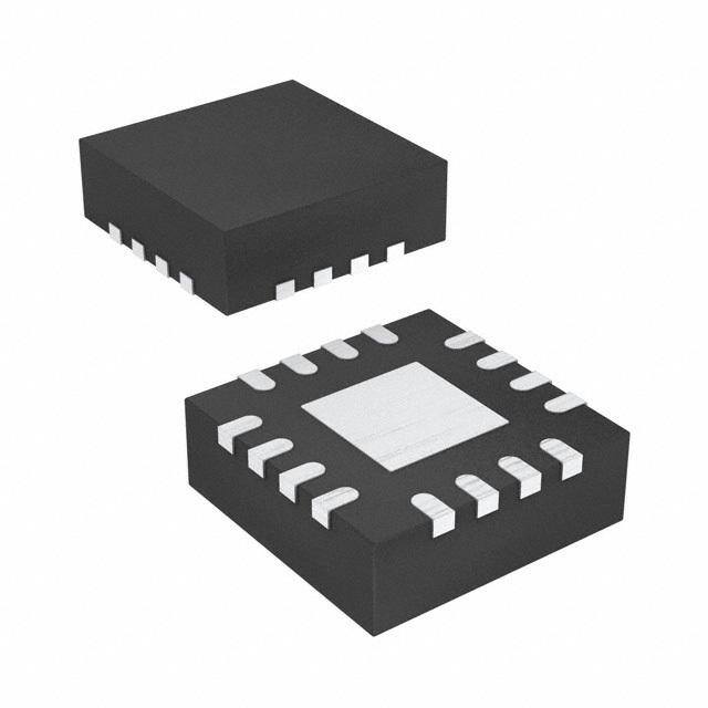
| 描述 | IC REG BUCK SYNC 2.5V 3A 16QFN稳压器—开关式稳压器 3A,2.5-6Vin,97% Eff Sync SD Converter |
| 产品分类 | |
| 品牌 | Texas Instruments |
| 产品手册 | |
| 产品图片 |
|
| rohs | 符合RoHS无铅 / 符合限制有害物质指令(RoHS)规范要求 |
| 产品系列 | 电源管理 IC,稳压器—开关式稳压器,Texas Instruments TPS62092RGTTDCS-Control™ |
| 数据手册 | |
| 产品型号 | TPS62092RGTT |
| PCN组件/产地 | |
| PWM类型 | 混合物 |
| 产品种类 | 稳压器—开关式稳压器 |
| 供应商器件封装 | 16-QFN(3x3) |
| 其它名称 | 296-30385-1 |
| 包装 | 剪切带 (CT) |
| 同步整流器 | 是 |
| 商标 | Texas Instruments |
| 安装类型 | 表面贴装 |
| 安装风格 | SMD/SMT |
| 封装 | Reel |
| 封装/外壳 | 16-VFQFN 裸露焊盘 |
| 封装/箱体 | VQFN-16 |
| 工作温度 | -40°C ~ 85°C |
| 工作温度范围 | - 40 C to + 85 C |
| 工厂包装数量 | 250 |
| 开关频率 | 2.8 MHz |
| 拓扑结构 | Buck |
| 最大工作温度 | + 85 C |
| 最大输入电压 | 6 V |
| 最小工作温度 | - 40 C |
| 最小输入电压 | 2.5 V |
| 标准包装 | 1 |
| 电压-输入 | 2.5 V ~ 6 V |
| 电压-输出 | 2.5V |
| 电流-输出 | 3A |
| 类型 | 降压(降压) |
| 系列 | TPS62092 |
| 设计资源 | http://www.digikey.com/product-highlights/cn/zh/texas-instruments-webench-design-center/3176 |
| 输入电压 | 2.5 V to 6 V |
| 输出数 | 1 |
| 输出电压 | 2.5 V |
| 输出电流 | 3 A |
| 输出端数量 | 1 Output |
| 输出类型 | 固定 |
| 频率-开关 | 2.8MHz |


.jpg)


- 商务部:美国ITC正式对集成电路等产品启动337调查
- 曝三星4nm工艺存在良率问题 高通将骁龙8 Gen1或转产台积电
- 太阳诱电将投资9.5亿元在常州建新厂生产MLCC 预计2023年完工
- 英特尔发布欧洲新工厂建设计划 深化IDM 2.0 战略
- 台积电先进制程称霸业界 有大客户加持明年业绩稳了
- 达到5530亿美元!SIA预计今年全球半导体销售额将创下新高
- 英特尔拟将自动驾驶子公司Mobileye上市 估值或超500亿美元
- 三星加码芯片和SET,合并消费电子和移动部门,撤换高东真等 CEO
- 三星电子宣布重大人事变动 还合并消费电子和移动部门
- 海关总署:前11个月进口集成电路产品价值2.52万亿元 增长14.8%


PDF Datasheet 数据手册内容提取
Product Order Technical Tools & Support & Folder Now Documents Software Community TPS62090,TPS62091,TPS62092,TPS62093 SLVSAW2C–MARCH2012–REVISEDOCTOBER2016 TPS6209x 3-A High Efficiency Synchronous Step Down Converter with DCS-Control™ 1 Features 3 Description • 2.5Vto6VInputVoltageRange The TPS6209x devices are a family of high frequency 1 synchronous step down converters optimized for • DCS-Control™ small solution size, high efficiency and suitable for • 95%ConverterEfficiency battery powered applications. To maximize efficiency, • PowerSaveMode the converters operate in pulse width modulation (PWM) mode with a nominal switching frequency of • 20µAOperatingQuiescentCurrent 2.8 MHz/1.4 MHz and automatically enter power save • 100%DutyCycleforLowestDropout mode operation at light load currents. When used in • 2.8MHz/1.4MHzTypicalSwitchingFrequency distributed power supplies and point of load regulation, the devices allow voltage tracking to other • 0.8VtoV AdjustableOutputVoltage IN voltage rails and tolerate output capacitors ranging • FixedOutputVoltageVersions from 10 µF up to 150 µF and beyond. Using the • OutputDischargeFunction DCS-Control™ topology the devices achieve • AdjustableSoftstart excellent load transient performance and accurate outputvoltageregulation. • HiccupShortCircuitProtection • OutputVoltageTracking The output voltage start-up ramp is controlled by the softstartpin,whichallowsoperationaseitherastand- • Pin-to-pincompatiblewithTPS62095 alone power supply or in tracking configurations. Power sequencing is also possible by configuring the 2 Applications enable and power good pins. In power save mode, • DistributedPowerSupplies the devices operate at typically 20 µA quiescent current. Power save mode is entered automatically • Notebook,NetbookComputers and seamlessly maintaining high efficiency over the • HardDiskDrivers(HDD) entireloadcurrentrange. • SolidStateDrives(SSD) DeviceInformation(1) • ProcessorSupply DEVICENAME PACKAGE BODYSIZE(NOM) • BatteryPoweredApplications TPS62090 TPS62091 QFN(16) 3.00mmx3.00mm TPS62092 TPS62093 (1) Forallavailablepackages,seetheorderableaddendumat theendofthedatasheet. sp sp TypicalApplicationSchematic EfficiencyvsOutputCurrent TPS62093 L1 100 Vin 470nH Vout 2.5 V to 6 V 12PVIN SW 1 1.8 V/3A 95 C1 11 PVIN SW 2 C2 90 10mF 22mF 10 AVIN VOS16 %) 85 1C03nF 1738 CCEPNN FREPFQGB 345 5PR0o30wkeΩr Good Efficiency ( 778050 C4 65 10nF 9 SP1S4GND P15GAGNDND 6 5650 VLf =O= U 20T. .8=4 M1µ.HH8z V VVVVIIIINNNN ==== 2345... 772V VVV Copyright © 2016,Texas Instruments Incorporated 50 100m 1 10 100 1k 10k I load (mA) G004 1 An IMPORTANT NOTICE at the end of this data sheet addresses availability, warranty, changes, use in safety-critical applications, intellectualpropertymattersandotherimportantdisclaimers.PRODUCTIONDATA.
TPS62090,TPS62091,TPS62092,TPS62093 SLVSAW2C–MARCH2012–REVISEDOCTOBER2016 www.ti.com Table of Contents 1 Features.................................................................. 1 8.4 DeviceFunctionalModes........................................11 2 Applications........................................................... 1 9 ApplicationandImplementation........................ 13 3 Description............................................................. 1 9.1 ApplicationInformation............................................13 4 RevisionHistory..................................................... 2 9.2 TypicalApplications................................................13 5 DeviceComparisonTable..................................... 3 10 PowerSupplyRecommendations..................... 19 6 PinConfigurationandFunctions......................... 3 11 Layout................................................................... 19 11.1 LayoutGuideline...................................................19 7 Specifications......................................................... 4 11.2 LayoutExample....................................................19 7.1 AbsoluteMaximumRatings......................................4 12 DeviceandDocumentationSupport................. 20 7.2 ESDRatings..............................................................4 7.3 RecommendedOperatingConditions.......................4 12.1 DeviceSupport ....................................................20 7.4 ThermalInformation..................................................4 12.2 RelatedLinks........................................................20 7.5 ElectricalCharacteristics...........................................5 12.3 ReceivingNotificationofDocumentationUpdates20 7.6 TypicalCharacteristics..............................................6 12.4 CommunityResources..........................................20 12.5 Trademarks...........................................................20 8 DetailedDescription.............................................. 7 12.6 ElectrostaticDischargeCaution............................20 8.1 Overview...................................................................7 12.7 Glossary................................................................20 8.2 FunctionalBlockDiagram.........................................8 13 Mechanical,Packaging,andOrderable 8.3 FeatureDescription...................................................8 Information........................................................... 21 4 Revision History NOTE:Pagenumbersforpreviousrevisionsmaydifferfrompagenumbersinthecurrentversion. ChangesfromRevisionB(April2014)toRevisionC Page • ChangedFeaturebullettextFrom"TwoLevel...."To"Hiccup...";and,deleted"WideOutputCapacitanceSelection" bullet....................................................................................................................................................................................... 1 • AddedCNandCPpinabsolutemaximumratings................................................................................................................. 4 • MovedStorageTempspectothe"AbsoluteMaximumRatings"table ................................................................................. 4 • AddedFeedbackvoltageaccuracyatT =25°C.................................................................................................................... 5 J • ChangedLegendinFigure2andFigure4toshowcorrectvoltages ................................................................................... 6 • UpdatedVoltageTracking(SS)section................................................................................................................................. 9 • AddedChargePump(CP,CN)section ............................................................................................................................... 11 • UpdatedPCBlayoutexample.............................................................................................................................................. 19 • AddedCommunityResourcessection................................................................................................................................. 20 ChangesfromRevisionA(March2012)toRevisionB Page • ChangedthedatasheettomeetthenewTIstandardFormat ............................................................................................. 1 • ChangedtheTypicalCharacteristics.MovedgraphstotheApplicationandImplementationsection................................... 6 • AddedtheLayoutsection .................................................................................................................................................... 19 ChangesfromOriginal(March2012)toRevisionA Page • ChangedtheFUNCTIONALBLOCKDIAGRAM.................................................................................................................... 8 • ChangedR1andR2valuesinFigure9............................................................................................................................... 13 2 SubmitDocumentationFeedback Copyright©2012–2016,TexasInstrumentsIncorporated ProductFolderLinks:TPS62090 TPS62091 TPS62092 TPS62093
TPS62090,TPS62091,TPS62092,TPS62093 www.ti.com SLVSAW2C–MARCH2012–REVISEDOCTOBER2016 5 Device Comparison Table DEVICENUMBER OUTPUTVOLTAGE TPS62090RGT Adjustable TPS62091RGT 3.3V TPS62092RGT 2.5V TPS62093RGT 1.8V 6 Pin Configuration and Functions RGTPackage 16-PinQFN TopView D D S N N O G G N V P P E 16 15 14 13 SW 1 12 PVIN SW 2 Exposed 11 PVIN Thermal Pad* FREQ 3 10 AVIN PG 4 9 SS 5 6 7 8 B D P N F N C C G A NOTE: *TheexposedthermalpadisconnectedtoAGND. PinFunctions PIN I/O DESCRIPTION NO. NAME 1,2 SW I/O Switchpinofthepowerstage. Thispinselectstheswitchingfrequencyofthedevice.FREQ=Lowsetsthetypicalswitchingfrequencyto2.8MHz.FREQ= 3 FREQ I Highsetsthetypicalswitchingfrequencyto1.4MHz.Thispinhasanactivepulldownresistoroftypically400kΩandcanbe leftfloatingfor2.8MHzoperation. Powergoodopendrainoutput.Thispinishighimpedanceiftheoutputvoltageiswithinregulation.Thispinispulledlowif 4 PG O theoutputisbelowitsnominalvalue.Thepullupresistorcannotbeconnectedtoanyvoltagehigherthantheinputvoltageof thedevice. Feedbackpinofthedevice. Fortheadjustableversion,connectaresistordividertosettheoutputvoltage. 5 FB I ForthefixedoutputvoltageversionsthispinmaybeconnectedtoGNDforimprovedthermalperformanceandhasapull downresistoroftypically400kΩ,whichisactivewhenENislow. 6 AGND Analogground. 7 CP I/O Internalchargepumpflyingcapacitor.Connecta10nFcapacitorbetweenCPandCN. 8 CN I/O Internalchargepumpflyingcapacitor.Connecta10nFcapacitorbetweenCPandCN. Softstartcontrolpin.Acapacitorisconnectedtothispinandsetsthesoftstarttime.Leavingthispinfloatingsetstheminimum 9 SS I start-uptime. 10 AVIN I Biassupplyinputvoltagepin. 11,12 PVIN I Powersupplyinputvoltagepin. Deviceenable.Toenablethedevicethispinneedstobepulledhigh.Pullingthispinlowdisablesthedevice.Thispinhasa 13 EN I pulldownresistoroftypically400kΩ,whichisactivewhenENislow. 14,15 PGND Powergroundconnection. 16 VOS I Outputvoltagesensepin.Thispinneedstobeconnectedtotheoutputvoltage. ExposedThermalPad – TheexposedthermalpadisconnectedtoAGND.Itmustbesolderedformechanicalreliability. Copyright©2012–2016,TexasInstrumentsIncorporated SubmitDocumentationFeedback 3 ProductFolderLinks:TPS62090 TPS62091 TPS62092 TPS62093
TPS62090,TPS62091,TPS62092,TPS62093 SLVSAW2C–MARCH2012–REVISEDOCTOBER2016 www.ti.com 7 Specifications 7.1 Absolute Maximum Ratings(1) Overoperatingfree-airtemperaturerange(unlessotherwisenoted) VALUE UNIT MIN MAX PVIN,AVIN,FB,SS,EN,FREQ,VOS –0.3 7 Voltagerange(2) SW,PG –0.3 V +0.3 V IN CN,CP -0.3 V +7.0 IN PowerGoodsinkcurrent PG 1 mA Operatingjunctiontemperature,T –40 150 °C J Storagetemperature,T –65 150 °C stg (1) Stressesbeyondthoselistedunder“absolutemaximumratings”maycausepermanentdamagetothedevice.Thesearestressratings onlyandfunctionaloperationofthedeviceattheseoranyotherconditionsbeyondthoseindicatedunder“recommendedoperating conditions”isnotimplied.Exposuretoabsolute–maximum–ratedconditionsforextendedperiodsmayaffectdevicereliability. (2) Allvoltagevaluesarewithrespecttonetworkgroundpin. 7.2 ESD Ratings VALUE UNIT Humanbodymodel(HBM)perANSI/ESDA/JEDECJS-001,allpins (1) ±2000 V Electrostatic V(ESD) discharge Cpihnasrg(2e)ddevicemodel(CDM),perJEDECspecificationJESD22-C101,all ±500 V (1) JEDECdocumentJEP155statesthat500-VHBMallowssafemanufacturingwithastandardESDcontrolprocess. (2) JEDECdocumentJEP157statesthat250-VCDMallowssafemanufacturingwithastandardESDcontrolprocess. 7.3 Recommended Operating Conditions(1) MIN TYP MAX UNIT V InputvoltagerangeV 2.5 6 V IN IN T Operatingambienttemperature –40 85 °C A T Operatingjunctiontemperature –40 125 °C J (1) Seetheapplicationsectionforfurtherinformation 7.4 Thermal Information TPS6209x THERMALMETRIC(1) UNIT QFN(16PINS) R Junction-to-ambientthermalresistance 47 °C/W θJA R Junction-to-case(top)thermalresistance 60 °C/W θJCtop R Junction-to-boardthermalresistance 20 °C/W θJB ψ Junction-to-topcharacterizationparameter 1.5 °C/W JT ψ Junction-to-boardcharacterizationparameter 20 °C/W JB R Junction-to-case(bottom)thermalresistance 5.3 °C/W θJCbot (1) Formoreinformationabouttraditionalandnewthermalmetrics,seetheSemiconductorandICPackageThermalMetricsapplication report(SPRA953). 4 SubmitDocumentationFeedback Copyright©2012–2016,TexasInstrumentsIncorporated ProductFolderLinks:TPS62090 TPS62091 TPS62092 TPS62093
TPS62090,TPS62091,TPS62092,TPS62093 www.ti.com SLVSAW2C–MARCH2012–REVISEDOCTOBER2016 7.5 Electrical Characteristics V =3.6V,T =–40°Cto85°C,typicalvaluesareatT =25°C(unlessotherwisenoted) IN A A PARAMETER TESTCONDITIONS MIN TYP MAX UNIT SUPPLY V Inputvoltagerange 2.5 6 V IN I Quiescentcurrent Notswitching,FB=FB+5%,intoPVINandAVIN 20 µA QIN I Shutdowncurrent IntoPVINandAVIN 0.6 5 µA sd Undervoltagelockoutthreshold V falling 2.1 2.2 2.3 V IN UVLO Undervoltagelockouthysteresis 200 mV Thermalshutdown Temperaturerising 150 ºC Thermalshutdownhysteresis 20 ºC ControlSIGNALSEN,FREQ V Highlevelinputvoltage V =2.5Vto6V 1 0.65 V H IN V Lowlevelinputvoltage V =2.5Vto6V 0.6 0.4 V L IN I Inputleakagecurrent EN,FREQ=GNDorV 10 100 nA lkg IN R Pulldownresistance 400 kΩ PD Softstart I Softstartcurrent 6.3 7.5 8.7 µA SS POWERGOOD Outputvoltagerising 93% 95% 97% V Powergoodthreshold th Outputvoltagefalling 88% 90% 92% V Lowlevelvoltage I =1mA 0.4 V L (sink) I PGsinkingcurrent 1 mA PG I Leakagecurrent V =3.6V 10 100 nA lkg PG POWERSWITCH HighsideFETon-resistance I =500mA 50 mΩ SW R DS(on) LowsideFETon-resistance I =500mA 40 mΩ SW HighsideFETswitchcurrent I 3.7 4.6 5.5 A LIM limit FREQ=GND,I =3A 2.8 MHz OUT f Switchingfrequency s FREQ=VIN,I =3A 1.4 MHz OUT OUTPUT V Outputvoltagerange 0.8 V V s IN R Outputdischargeresistor EN=GND,V =1.8V 200 Ω od OUT V Feedbackregulationvoltage 0.8 V FB V ≥V +1V,TPS62090adjustableoutputversion IN OUT I =1A,PWMmode,T =25°C -1% +1% OUT J Feedbackvoltage IOUT=1A,PWMmode -1.4% +1.4% VFB accuracy(1) (2)(3) I =0mA,FREQ=2.8MHz,V ≥0.8V,PFMmode -1.4% +3% OUT OUT I =0mA,FREQ=1.4MHz,V ≥1.2V,PFMmode -1.4% +3% OUT OUT I =0mA,FREQ=1.4MHz,V <1.2V,PFMmode -1.4% +3.7% OUT OUT I Feedbackinputbiascurrent V =0.8V,TPS62090adjustableoutputversion 10 100 nA FB FB V ≥V +1V,fixedoutputvoltage IN OUT V Outputvoltageaccuracy (2)(3) I =1A,PWMmode -1.4% +1.4% OUT OUT I =0mA,FREQ=HighandLow,PFMmode -1.4% +2.5% OUT Lineregulation V =1.8V,PWMoperation 0.016 %/V OUT Loadregulation V =1.8V,PWMoperation 0.04 %/A OUT (1) Foroutputvoltages<1.2V,usea2x22µFoutputcapacitancetoachieve+3%outputvoltageaccuracy. (2) Conditions:f=2.8MHz,L=0.47µH,C =22µForf=1.4MHz,L=1µH,C =22µF. OUT OUT (3) Formoreinformation,seethePowerSaveModeOperationsectionofthisdatasheet. Copyright©2012–2016,TexasInstrumentsIncorporated SubmitDocumentationFeedback 5 ProductFolderLinks:TPS62090 TPS62091 TPS62092 TPS62093
TPS62090,TPS62091,TPS62092,TPS62093 SLVSAW2C–MARCH2012–REVISEDOCTOBER2016 www.ti.com 7.6 Typical Characteristics 70 1600 1400 60 1200 :) 50 z) m kH 1000 ce ( 40 ncy ( 800 n e esista 30 Frequ 600 R 20 T8 5=(cid:131) 8C5 oC 400 A VIN = 2.8 V 10 TA2 5=(cid:131) 2C5 oC 200 VIN = 3.6 V TA-4 =0 (cid:131)-4C0 oC 0 VIN = 4.2 V 0 0 400m 800m 1.2 1.6 2 2.4 2.8 3.2 2.0 2.5 3.0 3.5 4.0 4.5 5.0 5.5 6.0 6.5 Load Current (A) G009 Input Voltage (V) C00 V =1.8V L=1µH f=1.4MHz OUT Figure1.HighSideFETOn-ResistancevsInputVoltage Figure2.SwitchingFrequencyvsLoadCurrent 2 3500 1.75 3000 1.5 Frequency (MHz) 010..72.5515 VOUT = 1.8 V Frequency (kHz) 1122050500000000 L = 1 µH 0.25 fI O=U T1 .=4 1M AHz 500 VVVIIINNN === 234...862 VVV 0 0 2 2.5 3 3.5 4 4.5 5 5.5 6 6.5 0 400m 800m 1.2 1.6 2 2.4 2.8 3.2 Voltage (V) Load Current (A) G010 G026 V =1.8V L=0.4µH f=2.8MHz OUT Figure3.SwitchingFrequencyvsInputVoltage Figure4.FrequencyvsLoadCurrent 3500 25 3000 20 2500 z) Frequency (kH 112050000000 VOUT = 1.8 V Current (µA) 1105 VL O=U 1T =µ H1.8 V TTAA == 8255 °°CC L = 0.4 µH 5 f = 1.4 MHz TA = −40 °C 500 f = 2.8 MHz IOUT = 1 A 0 0 2 2.5 3 3.5 4 4.5 5 5.5 6 6.5 2 2.5 3 3.5 4 4.5 5 5.5 6 6.5 Input Voltage (V) Voltage (V) G026 G011 Figure5.FrequencyvsInputVoltage Figure6.QuiescentCurrentvsInputVoltage 6 SubmitDocumentationFeedback Copyright©2012–2016,TexasInstrumentsIncorporated ProductFolderLinks:TPS62090 TPS62091 TPS62092 TPS62093
TPS62090,TPS62091,TPS62092,TPS62093 www.ti.com SLVSAW2C–MARCH2012–REVISEDOCTOBER2016 8 Detailed Description 8.1 Overview The TPS6209x synchronous switched mode converters are based on DCS-Control™ (direct control with seamless transition into power save mode). This is an advanced regulation topology that combines the advantagesofhystereticandvoltagemodecontrol. The DCS-Control™ topology operates in pulse width modulation (PWM) mode for medium to heavy load conditions and in power save mode at light load currents. In PWM, the converter operates with its nominal switching frequency of 2.8 MHz/1.4 MHz having a controlled frequency variation over the input voltage range. As the load current decreases, the converter enters power save mode, reducing the switching frequency and minimizing the IC quiescent current to achieve high efficiency over the entire load current range. DCS-Control™ supports both operation modes (PWM and PFM) using a single building block having a seamless transition from PWM to power save mode without effects on the output voltage. Fixed output voltage versions provide smallest solution size combined with lowest quiescent current. The TPS6209x family offers excellent DC voltage regulation and load transient regulation, combined with low output voltage ripple, minimizing interference with RF circuits. Copyright©2012–2016,TexasInstrumentsIncorporated SubmitDocumentationFeedback 7 ProductFolderLinks:TPS62090 TPS62091 TPS62092 TPS62093
TPS62090,TPS62091,TPS62092,TPS62093 SLVSAW2C–MARCH2012–REVISEDOCTOBER2016 www.ti.com 8.2 Functional Block Diagram PG CP CN PVIN PVIN Charge Pump VFB for Hiccup Gate driver current limit VREF #32 counter High Side Bandgap Current AVIN Undervoltage Sense Lockout Thermal shutdown EN M1 400kΩ(2) SW MOSFETDriver AGND Anti ShootThrough Converter Control SW Logic High=1.4 MHz FREQ Low= 2.8 MHz 400kΩ(2) M2 PGND PGND ramp Comparator Direct Control and VOS Compensation Timer R1(1) ton ErrorAmplifier Adjounsltyable FB R2(1) R3(1) Vref 400kΩ 0.8V Vin DCS-Control™ 200Ω Iss Voltage clamp Vref SS ÷1.56 Output voltage EN discharge M3 logic Copyright © 2016,Texas Instruments Incorporated (1) R1,R2,R3areimplementedinthefixedoutputvoltageversiononly. (2) Theresistorsaredisconnectedwhenthepinsarehigh. 8.3 Feature Description 8.3.1 EnableandDisable(EN) ThedeviceisenabledbysettingtheENpintoalogichigh.Accordingly,shutdownmodeisforcediftheENpinis pulled low with a shutdown current of typically 0.6 μA. In shutdown mode, the internal power switches as well as the entire control circuitry are turned off. An internal resistor of 200 Ω discharges the output through the VOS pin smoothly. An internal pull-down resistor of 400 kΩ is connected to the EN pin when the EN pin is low. The pulldownresistorisdisconnectedwhentheENpinishigh. 8 SubmitDocumentationFeedback Copyright©2012–2016,TexasInstrumentsIncorporated ProductFolderLinks:TPS62090 TPS62091 TPS62092 TPS62093
TPS62090,TPS62091,TPS62092,TPS62093 www.ti.com SLVSAW2C–MARCH2012–REVISEDOCTOBER2016 Feature Description (continued) 8.3.2 Softstart(SS)andHiccupCurrentLimitDuringStartup To minimize inrush current during start up, the device has an adjustable softstart depending on the capacitor value connected to the SS pin. The device charges the softstart capacitor with a constant current of typically 7.5 µA.Thefeedbackvoltagefollowsthisvoltagewithafractionof1.56untiltheinternalreferencevoltageof0.8Vis reached. The softstart operation is completed once the voltage at the softstart capacitor has reached typically 1.25 V. The soft-start time can be calculated using Equation 1. The larger the softstart capacitor the longer the softstarttime.TherelationbetweensoftstartvoltageandfeedbackvoltagecanbeestimatedusingEquation2. 1.25V t =C x SS SS 7.5μA (1) V V = SS FB 1.56 (2) During startup, the switch current limit is reduced to 1/3 (~1.5 A) of its typical current limit of 4.6 A. Once the output voltage exceeds typically 0.6 V, the current limit is released to its nominal value. The device provides a reduced load current of ~1.5 A when the output voltage is below typically 0.6 V. Due to this, a small or no softstart time may trigger the short circuit protection during startup especially for larger output capacitors. This is avoided by using a larger softstart capacitance to extend the softstart time. See Short Circuit Protection (Hiccup- Mode) for details of the reduced current limit during startup. Leaving the softstart pin floating sets the minimum start-uptime(around50µs). 8.3.3 VoltageTracking(SS) The SS pin is externally driven by another voltage source to achieve output voltage tracking. The application circuitisshowninFigure7.TheinternalreferencevoltagefollowsthevoltageattheSSpinwithafractionof1.56 until the internal reference voltage of 0.8 V is reached. The device achieves ratiometric or coincidental (simultaneous)outputtracking,asshowninFigure8. VOUT1 VOUT2 R1 R3 SS FB R2 R4 GND GND Copyright © 2017, Texas Instruments Incorporated Figure7. OutputVoltageTracking Copyright©2012–2016,TexasInstrumentsIncorporated SubmitDocumentationFeedback 9 ProductFolderLinks:TPS62090 TPS62091 TPS62092 TPS62093
TPS62090,TPS62091,TPS62092,TPS62093 SLVSAW2C–MARCH2012–REVISEDOCTOBER2016 www.ti.com Feature Description (continued) Voltage Voltage V V OUT1 OUT1 V V OUT2 OUT2 R3 æ R1ö 1 R3 æ R1ö 1 1+ <ç1+ ÷´ 1+ =ç1+ ÷´ R4 è R2ø 1.56 R4 è R2ø 1.56 t t a) RatiometricTracking b) CoincidentalTracking Figure8. VoltageTrackingOptions The R2 value should be set properly to achieve accurate voltage tracking by taking 7.5 μA soft startup current intoaccount.1kΩ orsmallerisasufficientvalueforR2. For decreasing the SS pin voltage, the device doesn't sink current from the output when the device is in power save mode. So the resulting decreases of the output voltage may be slower than the SS pin voltage if the load is light. When driving the SS pin with an external voltage, do not exceed the voltage rating of the SS pin which is 7 V. 8.3.4 ShortCircuitProtection(Hiccup-Mode) ThedeviceisprotectedagainsthardshortcircuitstoGNDandover-currentevents.Thisisimplementedbyatwo level short circuit protection. During start-up and when the output is shorted to GND the switch current limit is reducedto1/3ofitstypicalcurrentlimitof4.6A.Oncetheoutputvoltageexceedstypically0.6Vthecurrentlimit is released to its nominal value. The full current limit is implemented as a hiccup current limit. Once the internal current limit is triggered 32 times the device stops switching and starts a new start-up sequence after a typical delay time of 66 µs passed by. The device will go through these cycles until the high current condition is released. 8.3.5 OutputDischargeFunction To make sure the device starts up under defined conditions, the output gets discharged via the VOS pin with a typical discharge resistor of 200 Ω whenever the device shuts down. This happens when the device is disabled orifthermalshutdown,undervoltagelockoutorshortcircuithiccup-modeistriggered. 8.3.6 PowerGoodOutput(PG) Thepowergoodoutputislowwhentheoutputvoltageisbelowitsnominalvalue.Thepowergoodbecomeshigh impedance once the output is within 5% of regulation. The PG pin is an open drain output and is specified to typically sink up to 1 mA. This output requires a pull-up resistor to be monitored properly. The pull-up resistor cannot be connected to any voltage higher than the input voltage of the device. The PG output is low when the deviceisdisabled,inthermalshutdownorUVLO.ThePGoutputcanbeleftfloatingifunused. 10 SubmitDocumentationFeedback Copyright©2012–2016,TexasInstrumentsIncorporated ProductFolderLinks:TPS62090 TPS62091 TPS62092 TPS62093
TPS62090,TPS62091,TPS62092,TPS62093 www.ti.com SLVSAW2C–MARCH2012–REVISEDOCTOBER2016 Feature Description (continued) 8.3.7 FrequencySetPin(FREQ) The FREQ pin is a digital logic input which sets the nominal switching frequency. Pulling this pin to GND sets the nominal switching frequency to 2.8 MHz and pulling this pin high sets the nominal switching frequency to 1.4 MHz. Since this pin changes the switching frequency it also changes the on-time during pulse frequency modulation (PFM) mode. At 1.4 MHz the on-time is twice the on-time as operating at 2.8 MHz. This pin has an active pull-down resistor of typically 400 kΩ. For applications where efficiency is of highest importance, a lower switching frequency should be selected. A higher switching frequency allows the use of smaller external components,fasterloadtransientresponseandloweroutputvoltageripplewhenusingsameL-Cvalues. 8.3.8 UndervoltageLockout(UVLO) To avoid mis-operation of the device at low input voltages, an undervoltage lockout is included. UVLO shuts downthedeviceatinputvoltageslowerthantypically2.2Vwitha200mVhysteresis. 8.3.9 ThermalShutdown The device goes into thermal shutdown once the junction temperature exceeds typically 150°C with a 20°C hysteresis. 8.3.10 ChargePump(CP,CN) The CP and CN pins must attach to an external 10 nF capacitor to complete a charge pump for the gate driver. This capacitor must be rated for the input voltage. It is not recommended to connect any other circuits to the CP orCNpins. 8.4 Device Functional Modes 8.4.1 PulseWidthModulationOperation At medium to heavy load currents, the device operates with pulse width modulation (PWM) at a nominal switching frequency of 2.8 MHz or 1.4 MHz depending on the setting of the FREQ pin. As the load current decreases, the converter enters the power save mode operation reducing its switching frequency. The device enterspowersavemodeattheboundarytodiscontinuousconductionmode(DCM). 8.4.2 PowerSaveModeOperation As the load current decreases, the converter enters power save mode operation. During power save mode, the converter operates with reduced switching frequency maintaining high efficiency. The power save mode is based on a fixed on-time architecture following Equation 3. When operating at 1.4 MHz the on-time is twice as long as the on-time for 2.8 MHz operation. This results in larger output voltage ripple, as shown in Figure 19 and Figure 20, and slightly higher output voltage at no load, as shown in Figure 16 and Figure 17. To have the same output voltage ripple at 1.4 MHz during PFM mode, either the output capacitor or the inductor value needs to be increased. As an example, operating at 2.8 MHz using 0.47 µH inductor gives the same output voltage ripple as operatingwith1.4MHzusing1µHinductor. V OUT ton = ×360ns 2.8MHz V IN V OUT ton = ×360ns×2 1.4MHz V IN 2×I OUT f = æ V -V ö V -V ton2ç1+ IN OUT ÷ x IN OUT ç V ÷ L è OUT ø (3) In power save mode the output voltage rises slightly above the nominal output voltage in PWM mode, as shown in Figure 16 and Figure 17. This effect can be reduced by increasing the output capacitance or the inductor value. This effect can also be reduced by programming the output voltage of the TPS62090 lower than the target value. As an example, if the target output voltage is 3.3 V, then the TPS62090 can be programmed to 3.3 V – 0.8%. As a result the output voltage accuracy is now -2.2% to +2.2% instead of -1.4% to 3%. The output voltage accuracyinPFMoperationisreflectedintheelectricalspecificationtableandgivenfora22 µFoutputcapacitor. Copyright©2012–2016,TexasInstrumentsIncorporated SubmitDocumentationFeedback 11 ProductFolderLinks:TPS62090 TPS62091 TPS62092 TPS62093
TPS62090,TPS62091,TPS62092,TPS62093 SLVSAW2C–MARCH2012–REVISEDOCTOBER2016 www.ti.com Device Functional Modes (continued) 8.4.3 LowDropoutOperation(100%DutyCycle) The device offers low input to output voltage difference by entering 100% duty cycle mode. In this mode the high sideMOSFETswitchisconstantlyturnedon.Thisisparticularlyusefulinbatterypoweredapplicationstoachieve longest operation time by taking full advantage of the whole battery voltage range. The minimum input voltage wheretheoutputvoltagefallsbelowitsnominalregulationvalueisgivenby: V =V +I x(R +R ) (4) IN(min) OUT OUT DS(on) L Where: R =HighsideFETon-resistance DS(on) R =DCresistanceoftheinductor L 12 SubmitDocumentationFeedback Copyright©2012–2016,TexasInstrumentsIncorporated ProductFolderLinks:TPS62090 TPS62091 TPS62092 TPS62093
TPS62090,TPS62091,TPS62092,TPS62093 www.ti.com SLVSAW2C–MARCH2012–REVISEDOCTOBER2016 9 Application and Implementation NOTE Information in the following applications sections is not part of the TI component specification, and TI does not warrant its accuracy or completeness. TI’s customers are responsible for determining suitability of components for their purposes. Customers should validateandtesttheirdesignimplementationtoconfirmsystemfunctionality. 9.1 Application Information The TPS6209x 3 A family of devices, are high frequency synchronous step down converters optimized for small solutionsize,highefficiencyandsuitableforbatterypoweredapplications. 9.2 Typical Applications TPS62090 L1 Vin 470nH Vout 12 1 2.5 V to 6 V PVIN SW 1.2 V/3A R1 C1 11 PVIN SW 2 75 kΩ C2 10mF 22mF 10 16 AVIN VOS R2 13 EN FB 5 150 kΩ R3 C3 500 kΩ 10nF 7 4 CP PG 8 3 Power Good CN FREQ C4 10nF 9 6 SS AGND PGND PGND 14 15 Copyright © 2016,Texas Instruments Incorporated Figure9. 1.2VAdjustableVersionOperatingat2.8MHz 9.2.1 DesignRequirements The design guideline provides a component selection to operate the device within the recommended operating conditions. The design can be optimized for highest efficiency or smallest solution size and lowest output voltage ripple. For highest efficiency set the device switching frequency to 1.4 MHz (FREQ = High) and select the output filter components according to Table 3. For smallest solution size and lowest output voltage ripple set the device switching frequency to 2.8 MHz (FREQ = Low) and select the output filter components according to Table 2. For thefixedoutputvoltageoptionthefeedbackpinneedstobeconnectedtoGND. Table1showsthelistofcomponentsfortheApplicationCurves. Table1.ListofComponents REFERENCE DESCRIPTION MANUFACTURER TPS62090 Highefficiencystepdownconverter TexasInstruments CoilcraftXFL4020-102,TOKODEF252012C-R47,Coilcraft L1 Inductor:1uH,0.47uH,0.4uH XAL4020-401 C1 Ceramiccapacitor:10uF,22uF (6.3V,X5R,0603),(6.3V,X5R,0805) C2 Ceramiccapacitor:22uF (6.3V,X5R,0805) C3,C4 Ceramiccapacitor Standard R1,R2,R3 Resistor Standard Copyright©2012–2016,TexasInstrumentsIncorporated SubmitDocumentationFeedback 13 ProductFolderLinks:TPS62090 TPS62091 TPS62092 TPS62093
TPS62090,TPS62091,TPS62092,TPS62093 SLVSAW2C–MARCH2012–REVISEDOCTOBER2016 www.ti.com 9.2.2 DetailedDesignProcedure The first step is the selection of the output filter components. To simplify this process, Table 2 and Table 3 outline possible inductor and capacitor value combinations. Checked cells represent combinations that are provenforstabilitybysimulationandlab.Furthercombinationsshouldbecheckedforeachindividualapplication. Table2.OutputFilterSelection(2.8MHzOperation,FREQ=GND) OUTPUTCAPACITORVALUE[µF](2) INDUCTORVALUE[µH](1) 10 22 47 100 150 0.47 √(3) √ √ √ 1.0 √ √ √ √ √ 2.2 3.3 (1) Inductortoleranceandcurrentde-ratingisanticipated.Theeffectiveinductancecanvaryby+20%and -30%. (2) Capacitancetoleranceandbiasvoltagede-ratingisanticipated.Theeffectivecapacitancecanvaryby +20%and-50%. (3) Typicalapplicationconfiguration.Othercheckmarkindicatesalternativefiltercombinations Table3.OutputFilterSelection(1.4MHzOperation,FREQ=V ) IN OUTPUTCAPACITORVALUE[µF](2) INDUCTORVALUE[µH](1) 10 22 47 100 150 0.47 √ √ √ √ 1.0 √ √(3) √ √ √ 2.2 √ √ √ √ √ 3.3 (1) Inductortoleranceandcurrentde-ratingisanticipated.Theeffectiveinductancecanvaryby+20%and –30%. (2) Capacitancetoleranceandbiasvoltagede-ratingisanticipated.Theeffectivecapacitancecanvaryby +20%and–50%. (3) Typicalapplicationconfiguration.Othercheckmarkindicatesalternativefiltercombinations 9.2.2.1 InductorSelection The inductor selection is affected by several parameter like inductor ripple current, output voltage ripple, transitionpointintopowersavemode,andefficiency.SeeTable4fortypicalinductors. Table4.InductorSelection INDUCTORVALUE COMPONENTSUPPLIER(1) SIZE(LxWxHmm) Isat/DCR 0.6µH CoilcraftXAL4012-601 4x4x2.1 7.1A/9.5mΩ 1µH CoilcraftXAL4020-102 4x4x2.1 5.9A/13.2mΩ 1µH CoilcraftXFL4020-102 4x4x2.1 5.1A/10.8mΩ 0.47µH TOKODFE252012R47 2.5x2x1.2 3.7A/39mΩ 1µH TOKODFE2520121R0 2.5x2x1.2 3.0A/59mΩ 0.68µH TOKODFE322512R68 3.2x2.5x1.2 3.5A/37mΩ 1µH TOKODFE3225121R0 3.2x2.5x1.2 3.1A/45mΩ (1) SeeThird-PartyProductsDisclaimer In addition, the inductor has to be rated for the appropriate saturation current and DC resistance (DCR). Equation 6 calculates the maximum inductor current under static load conditions. The formula takes the converter efficiency into account. The converter efficiency can be taken from the data sheet graph`s or 80% can be used as a conservative approach. The calculation must be done for the maximum input voltage where the peakswitchcurrentishighest. 14 SubmitDocumentationFeedback Copyright©2012–2016,TexasInstrumentsIncorporated ProductFolderLinks:TPS62090 TPS62091 TPS62092 TPS62093
TPS62090,TPS62091,TPS62092,TPS62093 www.ti.com SLVSAW2C–MARCH2012–REVISEDOCTOBER2016 V æ V ö OUT x ç1 - OUT ÷ h ç V x h ÷ DI = è IN ø L f x L (5) DI I =I + L PEAK OUT 2 where: • ƒ=Converterswitchingfrequency(typical2.8MHzor1.4MHz) • L=Selectedinductorvalue • η=Estimatedconverterefficiency(usethenumberfromtheefficiencycurvesor0.80asanconservative assumption) (6) Note:Thecalculationmustbedoneforthemaximuminputvoltageoftheapplication Calculating the maximum inductor current using the actual operating conditions gives the minimum saturation current.Amarginof20%needstobeaddedtocoverforloadtransientsduringoperation. 9.2.2.2 InputandOutputCapacitorSelection For best output and input voltage filtering, low ESR (X5R or X7R) ceramic capacitors are recommended. The input capacitor minimizes input voltage ripple, suppresses input voltage spikes and provides a stable system rail for the device. A 10-μF or larger input capacitor is recommended when FREQ = Low and a 22-uF or larger when FREQ=High. The output capacitor value can range from 10 μF up to 150 μF and beyond. Load transient testing and measuring the bode plot are good ways to verify stability with larger capacitor values. The recommended typical output capacitor value is 22 μF (nominal) and can vary over a wide range as outline in the output filter selection table. For output voltages above 1.8 V, noise can cause duty cycle jitter. This does not degrade device performance.Usinganoutputcapacitorof2x22μF(nominal)foroutputvoltages >1.8Vavoidsdutycyclejitter. CeramiccapacitorhaveaDC-Biaseffect,whichhasastronginfluenceonthefinaleffectivecapacitance.Choose therightcapacitorcarefullyincombinationwithconsideringitspackagesizeandvoltagerating. 9.2.2.3 SettingtheOutputVoltage Theoutputvoltageissetbyanexternalresistordivideraccordingtothefollowingequations: æ R1ö æ R1ö VOUT =VFB ´ çè1+ R2÷ø =0.8V ´ çè1+ R2÷ø (7) V 0.8V R2= FB = » 160kΩ I 5μA FB (8) æV ö æV ö R1=R2 ´ ç OUT -1÷ =R2 ´ ç OUT - 1÷ è VFB ø è 0.8V ø (9) When sizing R2, in order to achieve low quiescent current and acceptable noise sensitivity, use a minimum of 5 µA for the feedback current I . Larger currents through R2 improve noise sensitivity and output voltage FB accuracy. Lowest current consumption and best output voltage accuracy can be achieved with the fixed output voltage versions. For the fixed output voltage versions, the FB pin can be left floating or connected to GND to improvethethermalperformance.Afeedforwardcapacitorisnotrequiredforproperoperation. Copyright©2012–2016,TexasInstrumentsIncorporated SubmitDocumentationFeedback 15 ProductFolderLinks:TPS62090 TPS62091 TPS62092 TPS62093
TPS62090,TPS62091,TPS62092,TPS62093 SLVSAW2C–MARCH2012–REVISEDOCTOBER2016 www.ti.com 9.2.2.4 ApplicationCurves 100 100 95 95 90 90 85 85 %) %) y ( 80 y ( 80 nc 75 nc 75 e e Effici 70 Effici 70 65 65 60 VOUT = 3.3 V VIN = 3.7 V 60 VOUT = 3.3 V VIN = 3.7 V 55 Lf == 11. 4µ HMHz VVIINN == 45. 2V V 55 Lf == 21. 8µ HMHz VVIINN == 45. 2V V 50 50 100m 1 10 100 1k 10k 100m 1 10 100 1k 10k I load (mA) I load (mA) G002 G001 Figure10.EfficiencyvsLoadCurrent Figure11.EfficiencyvsLoadCurrent 100 100 95 95 90 90 85 85 %) %) y ( 80 y ( 80 nc 75 nc 75 e e Effici 70 Effici 70 65 65 VIN = 2.7 V VIN = 2.7 V 60 VOUT = 1.8 V VIN = 3.7 V 60 VOUT = 1.8 V VIN = 3.7 V 55 Lf == 11. 4µ HMHz VVIINN == 45. 2V V 55 Lf == 20..84 MµHHz VVIINN == 45. 2V V 50 50 100m 1 10 100 1k 10k 100m 1 10 100 1k 10k I load (mA) I load (mA) G003 G004 Figure12.EfficiencyvsLoadCurrent Figure13.EfficiencyvsLoadCurrent 100 100 95 95 90 90 85 85 %) %) y ( 80 y ( 80 nc 75 nc 75 e e Effici 70 Effici 70 65 65 VIN = 2.7 V VIN = 2.7 V 60 VOUT = 1.05 V VIN = 3.7 V 60 VOUT = 1.05 V VIN = 3.7 V 55 Lf == 11..40 MµHHz VVIINN == 45. 2V V 55 Lf == 20..84 MµHHz VVIINN == 45. 2V V 50 50 100m 1 10 100 1k 10k 100m 1 10 100 1k 10k I load (mA) I load (mA) G005 G006 Figure14.EfficiencyvsLoadCurrent Figure15.EfficiencyvsLoadCurrent 16 SubmitDocumentationFeedback Copyright©2012–2016,TexasInstrumentsIncorporated ProductFolderLinks:TPS62090 TPS62091 TPS62092 TPS62093
TPS62090,TPS62091,TPS62092,TPS62093 www.ti.com SLVSAW2C–MARCH2012–REVISEDOCTOBER2016 1.83 1.83 VOUT = 1.8 V VIN = 5.0 V VOUT = 1.8 V VIN = 5.0 V 1.825 L = 1 µH VIN = 4.2 V 1.825 L = 0.4 µH VIN = 4.2 V f = 1.4 MHz VIN = 3.7 V f = 2.8 MHz VIN = 3.7 V 1.82 1.82 V) V) e ( 1.815 e ( 1.815 g g a a olt 1.81 olt 1.81 V V put 1.805 put 1.805 ut ut O O 1.8 1.8 1.795 1.795 1.79 1.79 100m 1 10 100 1k 10k 100m 1 10 100 1k 10k I load (mA) I load (mA) G007 G008 Figure16.OutputVoltagevsLoadCurrent Figure17.OutputVoltagevsLoadCurrent V V sw sw 2 V/div 2 V/div V V o o 20 mV/div 20 mV/div 1IinAdu/dctiovr VVf =ion= 1=1. .438 . M7V HV/3zA, L= 1 µH 500 mIinAdu/dctiovr VVf =ion =1= . 143. .8M7 VHV/z1,0 L0= m 1A µH 400 ns/div G012 1 µs/div G013 Figure18.PWMOperation Figure19.PFMOperation V o 20 mV/div V sw 2 V/div I o 1A/div V o 20 mV/div 500 mIinAdu/dctiovr VVf =ion =2= . 183. .8M7 VHV/z1,0 L0= m 0A.47 µH 500 mIinAdu/dctiovr VVf =ion =1= . 143. .8M7 VHVz, L= 1 µH 1 µs/div G014 200 µs/div G015 Figure20.PFMOperation Figure21.LoadSweep Copyright©2012–2016,TexasInstrumentsIncorporated SubmitDocumentationFeedback 17 ProductFolderLinks:TPS62090 TPS62091 TPS62092 TPS62093
TPS62090,TPS62091,TPS62092,TPS62093 SLVSAW2C–MARCH2012–REVISEDOCTOBER2016 www.ti.com V o 20 mV/div I V o EN 2A/div 2 V/div V o 1 V/div V = 3.7 V in I I inductor V = 1.8 V inductor o 500 mA/div 500 mA/div f = 2.8 MHz, L= 1 µH 200 µs/div G016 400 µs/div G017 V =1.8V/ f=2.8MHz/L= C =10nF O SS 600mA 1µH Figure22.LoadSweep Figure23.Start-Up V = 3.7 V in V = 1.8 V V o o f = 1.4 MHz, L= 1 µH 1 V/div V EN 2 V/div Io V 2A/div o 1 V/div I I inductor inductor 500 mA/div 1A/div 2 ms/div G018 40 µs/div G019 V =1.8V/No f=1.4MHz/L= O Load 1µH Figure25.HiccupShortCircuitProtection Figure24.Shutdown V o 1 V/div V o I 50 mV/div o 2A/div V = 3.7 V in V = 1.8 V o V = 3.7 V f = 1.4 MHz, L= 1 µH in V = 1.8 V, 0.3Ato 2.5A I I o inductor inductor f = 1.4 MHz, L= 1 µH 1A/div 1A/div C = 22 µF o 400 µs/div G020 40 µs/div G022 Figure26.HiccupShortCircuitProtection Figure27.LoadTransientResponse 18 SubmitDocumentationFeedback Copyright©2012–2016,TexasInstrumentsIncorporated ProductFolderLinks:TPS62090 TPS62091 TPS62092 TPS62093
TPS62090,TPS62091,TPS62092,TPS62093 www.ti.com SLVSAW2C–MARCH2012–REVISEDOCTOBER2016 V o 50 mV/div I o 1 V/div V = 3.7 V in V = 1.8 V, 20 mAto 1A I o inductor f = 1.4 MHz, L= 1 µH 500A/div C = 22 µF o 100 µs/div G023 Figure28.LoadTransientResponse 10 Power Supply Recommendations The power supply to the TPS62090 needs to have a current rating according to the supply voltage, output voltageandoutputcurrentoftheTPS62090. 11 Layout 11.1 Layout Guideline • ItisrecommendedtoplacetheinputcapacitorascloseaspossibletotheICpinsPVINandPGND. • The VOS connection is noise sensitive and needs to be routed as short and directly to the output pin of the inductor. • Theexposedthermalpadofthepackage,analogground(pin6)andpowerground(pin14,15)shouldhavea singlejointconnectionattheexposedthermalpadofthepackage.Thisminimizesswitchnodejitter. • ThechargepumpcapacitorconnectedtoCPandCNshouldbeplacedclosetotheICtominimizecouplingof switchingwaveformsintoothertracesandcircuits. • Refer to Figure 29 and the evaluation module User Guide (SLVU670) for an example of component placement,routingandthermaldesign. 11.2 Layout Example 1 L1 x R1 1 AGND L R2R2x1C5 VOUT PGFREQ SWSW C2 FB VOS AGND PGND CP PGND CN EN C4 SSAVINPVINPVIN VIN GND C1 Figure29. TPS6209xLayout Copyright©2012–2016,TexasInstrumentsIncorporated SubmitDocumentationFeedback 19 ProductFolderLinks:TPS62090 TPS62091 TPS62092 TPS62093
TPS62090,TPS62091,TPS62092,TPS62093 SLVSAW2C–MARCH2012–REVISEDOCTOBER2016 www.ti.com 12 Device and Documentation Support 12.1 Device Support 12.1.1 Third-PartyProductsDisclaimer TI'S PUBLICATION OF INFORMATION REGARDING THIRD-PARTY PRODUCTS OR SERVICES DOES NOT CONSTITUTE AN ENDORSEMENT REGARDING THE SUITABILITY OF SUCH PRODUCTS OR SERVICES OR A WARRANTY, REPRESENTATION OR ENDORSEMENT OF SUCH PRODUCTS OR SERVICES, EITHER ALONEORINCOMBINATIONWITHANYTIPRODUCTORSERVICE. 12.2 Related Links The table below lists quick access links. Categories include technical documents, support and community resources,toolsandsoftware,andquickaccesstosampleorbuy. Table5.RelatedLinks TECHNICAL TOOLS& SUPPORT& PARTS PRODUCTFOLDER SAMPLE&BUY DOCUMENTS SOFTWARE COMMUNITY TPS62090 Clickhere Clickhere Clickhere Clickhere Clickhere TPS62091 Clickhere Clickhere Clickhere Clickhere Clickhere TPS62092 Clickhere Clickhere Clickhere Clickhere Clickhere TPS62093 Clickhere Clickhere Clickhere Clickhere Clickhere 12.3 Receiving Notification of Documentation Updates To receive notification of documentation updates, navigate to the device product folder on ti.com. In the upper right corner, click on Alert me to register and receive a weekly digest of any product information that has changed.Forchangedetails,reviewtherevisionhistoryincludedinanyreviseddocument. 12.4 Community Resources The following links connect to TI community resources. Linked contents are provided "AS IS" by the respective contributors. They do not constitute TI specifications and do not necessarily reflect TI's views; see TI's Terms of Use. TIE2E™OnlineCommunity TI'sEngineer-to-Engineer(E2E)Community.Createdtofostercollaboration amongengineers.Ate2e.ti.com,youcanaskquestions,shareknowledge,exploreideasandhelp solveproblemswithfellowengineers. DesignSupport TI'sDesignSupport QuicklyfindhelpfulE2Eforumsalongwithdesignsupporttoolsand contactinformationfortechnicalsupport. 12.5 Trademarks DCS-Control,E2EaretrademarksofTexasInstruments. Allothertrademarksarethepropertyoftheirrespectiveowners. 12.6 Electrostatic Discharge Caution Thesedeviceshavelimitedbuilt-inESDprotection.Theleadsshouldbeshortedtogetherorthedeviceplacedinconductivefoam duringstorageorhandlingtopreventelectrostaticdamagetotheMOSgates. 12.7 Glossary SLYZ022—TIGlossary. Thisglossarylistsandexplainsterms,acronyms,anddefinitions. 20 SubmitDocumentationFeedback Copyright©2012–2016,TexasInstrumentsIncorporated ProductFolderLinks:TPS62090 TPS62091 TPS62092 TPS62093
TPS62090,TPS62091,TPS62092,TPS62093 www.ti.com SLVSAW2C–MARCH2012–REVISEDOCTOBER2016 13 Mechanical, Packaging, and Orderable Information The following pages include mechanical, packaging, and orderable information. This information is the most current data available for the designated devices. This data is subject to change without notice and revision of thisdocument.Forbrowser-basedversionsofthisdatasheet,refertotheleft-handnavigation. Copyright©2012–2016,TexasInstrumentsIncorporated SubmitDocumentationFeedback 21 ProductFolderLinks:TPS62090 TPS62091 TPS62092 TPS62093
PACKAGE OPTION ADDENDUM www.ti.com 6-Feb-2020 PACKAGING INFORMATION Orderable Device Status Package Type Package Pins Package Eco Plan Lead/Ball Finish MSL Peak Temp Op Temp (°C) Device Marking Samples (1) Drawing Qty (2) (6) (3) (4/5) TPS62090RGTR ACTIVE VQFN RGT 16 3000 Green (RoHS NIPDAU Level-2-260C-1 YEAR -40 to 85 SBW & no Sb/Br) TPS62090RGTT ACTIVE VQFN RGT 16 250 Green (RoHS NIPDAU Level-2-260C-1 YEAR -40 to 85 SBW & no Sb/Br) TPS62091RGTR ACTIVE VQFN RGT 16 3000 Green (RoHS NIPDAU Level-2-260C-1 YEAR -40 to 85 SBX & no Sb/Br) TPS62091RGTT ACTIVE VQFN RGT 16 250 Green (RoHS NIPDAU Level-2-260C-1 YEAR -40 to 85 SBX & no Sb/Br) TPS62092RGTR ACTIVE VQFN RGT 16 3000 Green (RoHS NIPDAU Level-2-260C-1 YEAR -40 to 85 SBY & no Sb/Br) TPS62092RGTT ACTIVE VQFN RGT 16 250 Green (RoHS NIPDAU Level-2-260C-1 YEAR -40 to 85 SBY & no Sb/Br) TPS62093RGTR ACTIVE VQFN RGT 16 3000 Green (RoHS NIPDAU Level-2-260C-1 YEAR -40 to 85 SBZ & no Sb/Br) TPS62093RGTT ACTIVE VQFN RGT 16 250 Green (RoHS NIPDAU Level-2-260C-1 YEAR -40 to 85 SBZ & no Sb/Br) (1) The marketing status values are defined as follows: ACTIVE: Product device recommended for new designs. LIFEBUY: TI has announced that the device will be discontinued, and a lifetime-buy period is in effect. NRND: Not recommended for new designs. Device is in production to support existing customers, but TI does not recommend using this part in a new design. PREVIEW: Device has been announced but is not in production. Samples may or may not be available. OBSOLETE: TI has discontinued the production of the device. (2) RoHS: TI defines "RoHS" to mean semiconductor products that are compliant with the current EU RoHS requirements for all 10 RoHS substances, including the requirement that RoHS substance do not exceed 0.1% by weight in homogeneous materials. Where designed to be soldered at high temperatures, "RoHS" products are suitable for use in specified lead-free processes. TI may reference these types of products as "Pb-Free". RoHS Exempt: TI defines "RoHS Exempt" to mean products that contain lead but are compliant with EU RoHS pursuant to a specific EU RoHS exemption. Green: TI defines "Green" to mean the content of Chlorine (Cl) and Bromine (Br) based flame retardants meet JS709B low halogen requirements of <=1000ppm threshold. Antimony trioxide based flame retardants must also meet the <=1000ppm threshold requirement. (3) MSL, Peak Temp. - The Moisture Sensitivity Level rating according to the JEDEC industry standard classifications, and peak solder temperature. (4) There may be additional marking, which relates to the logo, the lot trace code information, or the environmental category on the device. Addendum-Page 1
PACKAGE OPTION ADDENDUM www.ti.com 6-Feb-2020 (5) Multiple Device Markings will be inside parentheses. Only one Device Marking contained in parentheses and separated by a "~" will appear on a device. If a line is indented then it is a continuation of the previous line and the two combined represent the entire Device Marking for that device. (6) Lead/Ball Finish - Orderable Devices may have multiple material finish options. Finish options are separated by a vertical ruled line. Lead/Ball Finish values may wrap to two lines if the finish value exceeds the maximum column width. Important Information and Disclaimer:The information provided on this page represents TI's knowledge and belief as of the date that it is provided. TI bases its knowledge and belief on information provided by third parties, and makes no representation or warranty as to the accuracy of such information. Efforts are underway to better integrate information from third parties. TI has taken and continues to take reasonable steps to provide representative and accurate information but may not have conducted destructive testing or chemical analysis on incoming materials and chemicals. TI and TI suppliers consider certain information to be proprietary, and thus CAS numbers and other limited information may not be available for release. In no event shall TI's liability arising out of such information exceed the total purchase price of the TI part(s) at issue in this document sold by TI to Customer on an annual basis. OTHER QUALIFIED VERSIONS OF TPS62090 : •Automotive: TPS62090-Q1 NOTE: Qualified Version Definitions: •Automotive - Q100 devices qualified for high-reliability automotive applications targeting zero defects Addendum-Page 2
PACKAGE MATERIALS INFORMATION www.ti.com 20-Jul-2019 TAPE AND REEL INFORMATION *Alldimensionsarenominal Device Package Package Pins SPQ Reel Reel A0 B0 K0 P1 W Pin1 Type Drawing Diameter Width (mm) (mm) (mm) (mm) (mm) Quadrant (mm) W1(mm) TPS62090RGTR VQFN RGT 16 3000 330.0 12.4 3.3 3.3 1.1 8.0 12.0 Q2 TPS62090RGTR VQFN RGT 16 3000 330.0 12.4 3.3 3.3 1.1 8.0 12.0 Q2 TPS62090RGTT VQFN RGT 16 250 180.0 12.5 3.3 3.3 1.1 8.0 12.0 Q2 TPS62090RGTT VQFN RGT 16 250 180.0 12.4 3.3 3.3 1.1 8.0 12.0 Q2 TPS62091RGTR VQFN RGT 16 3000 330.0 12.4 3.3 3.3 1.1 8.0 12.0 Q2 TPS62091RGTT VQFN RGT 16 250 180.0 12.5 3.3 3.3 1.1 8.0 12.0 Q2 TPS62092RGTR VQFN RGT 16 3000 330.0 12.4 3.3 3.3 1.1 8.0 12.0 Q2 TPS62092RGTT VQFN RGT 16 250 180.0 12.5 3.3 3.3 1.1 8.0 12.0 Q2 TPS62093RGTR VQFN RGT 16 3000 330.0 12.4 3.3 3.3 1.1 8.0 12.0 Q2 TPS62093RGTT VQFN RGT 16 250 180.0 12.5 3.3 3.3 1.1 8.0 12.0 Q2 PackMaterials-Page1
PACKAGE MATERIALS INFORMATION www.ti.com 20-Jul-2019 *Alldimensionsarenominal Device PackageType PackageDrawing Pins SPQ Length(mm) Width(mm) Height(mm) TPS62090RGTR VQFN RGT 16 3000 367.0 367.0 35.0 TPS62090RGTR VQFN RGT 16 3000 338.0 355.0 50.0 TPS62090RGTT VQFN RGT 16 250 338.0 355.0 50.0 TPS62090RGTT VQFN RGT 16 250 210.0 185.0 35.0 TPS62091RGTR VQFN RGT 16 3000 338.0 355.0 50.0 TPS62091RGTT VQFN RGT 16 250 338.0 355.0 50.0 TPS62092RGTR VQFN RGT 16 3000 338.0 355.0 50.0 TPS62092RGTT VQFN RGT 16 250 338.0 355.0 50.0 TPS62093RGTR VQFN RGT 16 3000 338.0 355.0 50.0 TPS62093RGTT VQFN RGT 16 250 338.0 355.0 50.0 PackMaterials-Page2
None
PACKAGE OUTLINE RGT0016C VQFN - 1 mm max height SCALE 3.600 PLASTIC QUAD FLATPACK - NO LEAD A 3.1 B 2.9 PIN 1 INDEX AREA 3.1 2.9 1 MAX C SEATING PLANE 0.05 0.08 0.00 1.68 0.07 (0.2) TYP 5 8 EXPOSED THERMAL PAD 12X 0.5 4 9 4X SYMM 1.5 1 12 0.30 16X 0.18 16 13 0.1 C A B PIN 1 ID SYMM (OPTIONAL) 0.05 0.5 16X 0.3 4222419/B 11/2016 NOTES: 1. All linear dimensions are in millimeters. Any dimensions in parenthesis are for reference only. Dimensioning and tolerancing per ASME Y14.5M. 2. This drawing is subject to change without notice. 3. The package thermal pad must be soldered to the printed circuit board for thermal and mechanical performance. www.ti.com
EXAMPLE BOARD LAYOUT RGT0016C VQFN - 1 mm max height PLASTIC QUAD FLATPACK - NO LEAD ( 1.68) SYMM 16 13 16X (0.6) 1 12 16X (0.24) SYMM (2.8) (0.58) TYP 12X (0.5) 9 4 ( 0.2) TYP VIA 5 8 (R0.05) (0.58) TYP ALL PAD CORNERS (2.8) LAND PATTERN EXAMPLE SCALE:20X 0.07 MAX 0.07 MIN ALL AROUND ALL AROUND SOLDER MASK METAL OPENING SOLDER MASK METAL UNDER OPENING SOLDER MASK NON SOLDER MASK SOLDER MASK DEFINED DEFINED (PREFERRED) SOLDER MASK DETAILS 4222419/B 11/2016 NOTES: (continued) 4. This package is designed to be soldered to a thermal pad on the board. For more information, see Texas Instruments literature number SLUA271 (www.ti.com/lit/slua271). 5. Vias are optional depending on application, refer to device data sheet. If any vias are implemented, refer to their locations shown on this view. It is recommended that vias under paste be filled, plugged or tented. www.ti.com
EXAMPLE STENCIL DESIGN RGT0016C VQFN - 1 mm max height PLASTIC QUAD FLATPACK - NO LEAD ( 1.55) 16 13 16X (0.6) 1 12 16X (0.24) 17 SYMM (2.8) 12X (0.5) 9 4 METAL ALL AROUND 5 8 SYMM (R0.05) TYP (2.8) SOLDER PASTE EXAMPLE BASED ON 0.125 mm THICK STENCIL EXPOSED PAD 17: 85% PRINTED SOLDER COVERAGE BY AREA UNDER PACKAGE SCALE:25X 4222419/B 11/2016 NOTES: (continued) 6. Laser cutting apertures with trapezoidal walls and rounded corners may offer better paste release. IPC-7525 may have alternate design recommendations. www.ti.com
IMPORTANTNOTICEANDDISCLAIMER TI PROVIDES TECHNICAL AND RELIABILITY DATA (INCLUDING DATASHEETS), DESIGN RESOURCES (INCLUDING REFERENCE DESIGNS), APPLICATION OR OTHER DESIGN ADVICE, WEB TOOLS, SAFETY INFORMATION, AND OTHER RESOURCES “AS IS” AND WITH ALL FAULTS, AND DISCLAIMS ALL WARRANTIES, EXPRESS AND IMPLIED, INCLUDING WITHOUT LIMITATION ANY IMPLIED WARRANTIES OF MERCHANTABILITY, FITNESS FOR A PARTICULAR PURPOSE OR NON-INFRINGEMENT OF THIRD PARTY INTELLECTUAL PROPERTY RIGHTS. These resources are intended for skilled developers designing with TI products. You are solely responsible for (1) selecting the appropriate TI products for your application, (2) designing, validating and testing your application, and (3) ensuring your application meets applicable standards, and any other safety, security, or other requirements. These resources are subject to change without notice. TI grants you permission to use these resources only for development of an application that uses the TI products described in the resource. Other reproduction and display of these resources is prohibited. No license is granted to any other TI intellectual property right or to any third party intellectual property right. TI disclaims responsibility for, and you will fully indemnify TI and its representatives against, any claims, damages, costs, losses, and liabilities arising out of your use of these resources. TI’s products are provided subject to TI’s Terms of Sale (www.ti.com/legal/termsofsale.html) or other applicable terms available either on ti.com or provided in conjunction with such TI products. TI’s provision of these resources does not expand or otherwise alter TI’s applicable warranties or warranty disclaimers for TI products. Mailing Address: Texas Instruments, Post Office Box 655303, Dallas, Texas 75265 Copyright © 2020, Texas Instruments Incorporated