ICGOO在线商城 > 集成电路(IC) > PMIC - 稳压器 - DC DC 开关稳压器 > TPS62065DSGR
 Datasheet下载
- 型号: TPS62065DSGR
- 制造商: Texas Instruments
- 库位|库存: xxxx|xxxx
- 要求:
| 数量阶梯 | 香港交货 | 国内含税 |
| +xxxx | $xxxx | ¥xxxx |
查看当月历史价格
查看今年历史价格
TPS62065DSGR产品简介:
ICGOO电子元器件商城为您提供TPS62065DSGR由Texas Instruments设计生产,在icgoo商城现货销售,并且可以通过原厂、代理商等渠道进行代购。 TPS62065DSGR价格参考。Texas InstrumentsTPS62065DSGR封装/规格:PMIC - 稳压器 - DC DC 开关稳压器, 可调式 降压 开关稳压器 IC 正 0.8V 1 输出 2A 8-WFDFN 裸露焊盘。您可以下载TPS62065DSGR参考资料、Datasheet数据手册功能说明书,资料中有TPS62065DSGR 详细功能的应用电路图电压和使用方法及教程。
TPS62065DSGR是德州仪器(Texas Instruments)推出的一款高效、低功耗的同步降压DC-DC开关稳压器。它主要应用于需要高效率和小尺寸解决方案的便携式电子设备中,如智能手机、平板电脑、笔记本电脑、可穿戴设备等。

该器件具有以下特点:

1. 宽输入电压范围:支持2.9V至5.5V的输入电压范围,适用于单节锂离子电池供电或低压直流电源系统。
2. 高效转换:在轻载和重载条件下均能保持较高的转换效率,有助于延长电池寿命。
3. 低静态电流:典型值仅为17μA,适合对功耗要求极高的应用场合。
4. 快速瞬态响应:能够迅速响应负载变化,确保输出电压稳定,特别适合处理器、FPGA等需要快速动态响应的应用。
5. 内置补偿电路:简化了外部元件选择,减少了PCB布局复杂度。
6. 保护功能:具备过温、过流保护机制,提高了系统的可靠性。

此外,TPS62065DSGR采用小型封装(DSG, 8-bump),有助于节省空间,非常适合紧凑型设计。其固定输出电压版本提供多种预设选项(如1.8V、3.3V等),用户也可以通过外接电阻分压器来调整输出电压。

总之,TPS62065DSGR凭借其高性能和灵活性,在各种便携式电子产品中得到了广泛应用,尤其适用于那些对体积、功耗和成本有严格要求的产品。
| 参数 | 数值 |
| 产品目录 | 集成电路 (IC)半导体 |
| 描述 | IC REG BUCK SYNC ADJ 2A 8WSON稳压器—开关式稳压器 3MHz 2A Step-Down Converter |
| DevelopmentKit | TPS62065-67EVM-347 |
| 产品分类 | |
| 品牌 | Texas Instruments |
| 产品手册 | http://www.ti.com/litv/slvs833b |
| 产品图片 |
|
| rohs | 符合RoHS无铅 / 符合限制有害物质指令(RoHS)规范要求 |
| 产品系列 | 电源管理 IC,稳压器—开关式稳压器,Texas Instruments TPS62065DSGR- |
| 数据手册 | |
| 产品型号 | TPS62065DSGR |
| PCN组件/产地 | |
| PWM类型 | 电压模式 |
| 产品种类 | 稳压器—开关式稳压器 |
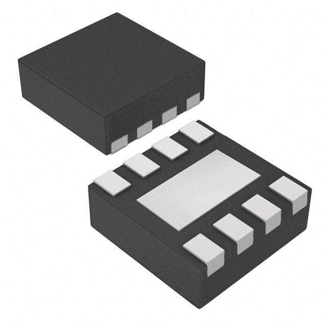
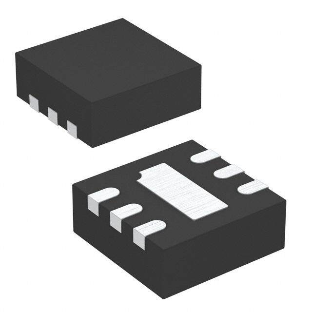
| 供应商器件封装 | 8-WSON (2x2) |
| 包装 | 带卷 (TR) |
| 同步整流器 | 是 |
| 商标 | Texas Instruments |
| 安装类型 | 表面贴装 |
| 安装风格 | SMD/SMT |
| 封装 | Reel |
| 封装/外壳 | 8-WFDFN 裸露焊盘 |
| 封装/箱体 | WSON-8 |
| 工作温度 | -40°C ~ 85°C |
| 工厂包装数量 | 3000 |
| 开关频率 | 3 MHz |
| 最大工作温度 | + 85 C |
| 最大输入电压 | 6 V |
| 最小工作温度 | - 40 C |
| 最小输入电压 | 3 V |
| 标准包装 | 3,000 |
| 电压-输入 | 3 V ~ 6 V |
| 电压-输出 | 0.8 V ~ 6 V |
| 电流-输出 | 2A |
| 类型 | Voltage Converter |
| 系列 | TPS62065 |
| 设计资源 | http://www.digikey.com/product-highlights/cn/zh/texas-instruments-webench-design-center/3176 |
| 负载调节 | - 0.5 % |
| 输出数 | 1 |
| 输出电压 | Adj |
| 输出电流 | 2 A |
| 输出类型 | 可调式 |
| 配用 | /product-detail/zh/TPS62065-67EVM-347/296-31246-ND/2353739 |
| 频率-开关 | 3MHz |


- 商务部:美国ITC正式对集成电路等产品启动337调查
- 曝三星4nm工艺存在良率问题 高通将骁龙8 Gen1或转产台积电
- 太阳诱电将投资9.5亿元在常州建新厂生产MLCC 预计2023年完工
- 英特尔发布欧洲新工厂建设计划 深化IDM 2.0 战略
- 台积电先进制程称霸业界 有大客户加持明年业绩稳了
- 达到5530亿美元!SIA预计今年全球半导体销售额将创下新高
- 英特尔拟将自动驾驶子公司Mobileye上市 估值或超500亿美元
- 三星加码芯片和SET,合并消费电子和移动部门,撤换高东真等 CEO
- 三星电子宣布重大人事变动 还合并消费电子和移动部门
- 海关总署:前11个月进口集成电路产品价值2.52万亿元 增长14.8%


PDF Datasheet 数据手册内容提取
Product Order Technical Tools & Support & Reference Folder Now Documents Software Community Design TPS62065,TPS62067 SLVS833D–MARCH2010–REVISEDNOVEMBER2016 TPS6206x 3-MHz, 2-A, Step-Down Converter in 2-mm × 2-mm SON Package 1 Features 3 Description • 3-MHzSwitchingFrequency The TPS6206x is a family of highly efficient 1 synchronous step down DC/DC converters. They • V Rangefrom2.9Vto6V IN provideupto2-Aoutputcurrent. • Upto97%Efficiency With an input voltage range of 2.9 V to 6 V, the • PowerSaveMode/3-MHzFixedPWMMode device is a perfect fit for power conversion from a 5-V • PowerGoodOutput or 3.3-V system supply rail. The TPS6206x operates • OutputVoltageAccuracyinPWMMode±1.5% at 3-MHz fixed frequency and enters power save mode operation at light load currents to maintain high • OutputCapacitorDischargeFunction efficiency over the entire load current range. The • Typical18µAQuiescentCurrent power save mode is optimized for low output voltage • 100%DutyCycleforLowestDropout ripple. For low noise applications, TPS62065 can be forced into fixed frequency PWM mode by pulling the • VoltagePositioning MODE pin high. TPS62067 provides an open drain • ClockDithering powergoodoutput. • -40°Cto125°COperatingJunctionTemperature In the shutdown mode, the current consumption is • SupportsMaximum1-mmHeightSolutions reduced to less than 1 µA and an internal circuit • Availableina2mmx2mmx0.75mmWSON dischargestheoutputcapacitor. TPS6206x family is optimized for operation with a tiny 2 Applications 1 µH inductor and a small 10-µF output capacitor to • PointofLoad(POL) achieve smallest solution size and high regulation performance. • Notebooks,PocketPCs • PortableMediaPlayers It is available in a small 2-mm × 2-mm × 0.75-mm 8- pinWSONpackage. • DSPSupply DeviceInformation(1) PARTNUMBER PACKAGE BODYSIZE(NOM) TPS62065 WSON(8) 2.00mm×2.00mm TPS62067 (1) For all available packages, see the orderable addendum at theendofthedatasheet. EfficiencyvsLoadCurrent 100 VIN= 3.7 V 95 TypicalApplicationSchematic 90 L V VIN= 4.2 V VIN= 5 V VIN= 2.9 V to 6 V 1.0mH 1.O8U VT 2A 85 PVIN SW % 80 AVIN R1 y - C10INmF AEGNND FB 3R620 kW C22ff pFC10OUmTF R10P0G kW Efficienc 7705 PGND 180 kW 65 PG L= 1.2mH (NRG4026T 1R2), 60 C = 22mF (0603 size), OUT Copyright©2016,TexasInstrumentsIncorporated VOUT= 3.3 V, 55 Mode:Auto PFM/PWM 50 0 0.25 0.5 0.75 1 1.25 1.5 1.75 2 IL- Load Current -A 1 An IMPORTANT NOTICE at the end of this data sheet addresses availability, warranty, changes, use in safety-critical applications, intellectualpropertymattersandotherimportantdisclaimers.PRODUCTIONDATA.
TPS62065,TPS62067 SLVS833D–MARCH2010–REVISEDNOVEMBER2016 www.ti.com Table of Contents 1 Features.................................................................. 1 9 ApplicationandImplementation........................ 12 2 Applications........................................................... 1 9.1 ApplicationInformation............................................12 3 Description............................................................. 1 9.2 TypicalApplication..................................................12 4 RevisionHistory..................................................... 2 9.3 SystemExample.....................................................18 5 DeviceComparisonTable..................................... 3 10 PowerSupplyRecommendations..................... 19 6 PinConfigurationandFunctions......................... 3 11 Layout................................................................... 19 11.1 LayoutGuidelines.................................................19 7 Specifications......................................................... 4 11.2 LayoutExample....................................................19 7.1 AbsoluteMaximumRatings......................................4 12 DeviceandDocumentationSupport................. 20 7.2 ESDRatings..............................................................4 7.3 RecommendedOperatingConditions.......................4 12.1 DeviceSupport......................................................20 7.4 ThermalInformation..................................................4 12.2 RelatedLinks........................................................20 7.5 ElectricalCharacteristics...........................................5 12.3 ReceivingNotificationofDocumentationUpdates20 7.6 TypicalCharacteristics..............................................6 12.4 CommunityResources..........................................20 12.5 Trademarks...........................................................20 8 DetailedDescription.............................................. 7 12.6 ElectrostaticDischargeCaution............................20 8.1 Overview...................................................................7 12.7 Glossary................................................................20 8.2 FunctionalBlockDiagram.........................................7 13 Mechanical,Packaging,andOrderable 8.3 FeatureDescription...................................................8 Information........................................................... 20 8.4 DeviceFunctionalModes..........................................9 4 Revision History NOTE:Pagenumbersforpreviousrevisionsmaydifferfrompagenumbersinthecurrentversion. ChangesfromRevisionC(September2015)toRevisionD Page • ChangedtheconditionsstatementfortheElectricalCharacteristics .................................................................................... 5 • AddedNote1totheTestconditionsofI ,I ,andI intheElectricalCharacteristics...................................................... 5 SD IN LKG • ChangedtemperaturevaluesFrom:T To:T inFigure1andFigure3 .............................................................................. 6 A J ChangesfromRevisionB(November2013)toRevisionC Page • AddedPinConfigurationandFunctionssection,ESDRatingstable,FeatureDescriptionsection,DeviceFunctional Modes,ApplicationandImplementationsection,PowerSupplyRecommendationssection,Layoutsection,Device andDocumentationSupportsection,andMechanical,Packaging,andOrderableInformationsection .............................. 1 ChangesfromRevisionA(May2010)toRevisionB Page • AddedThermalInformationtableanddeletedDissipationRatingstable.............................................................................. 5 ChangesfromOriginal(March2010)toRevisionA Page • ChangedV Rangefrom"3Vto6V"to"2.9Vto6V",throughout.......................................................................................... 1 IN • Addedequationto"OutputVoltageSetting"section............................................................................................................ 12 • Changedequationforcalculatingf ..................................................................................................................................... 12 z. • ChangedequationforcalculatingC ................................................................................................................................... 12 ff. 2 SubmitDocumentationFeedback Copyright©2010–2016,TexasInstrumentsIncorporated ProductFolderLinks:TPS62065 TPS62067
TPS62065,TPS62067 www.ti.com SLVS833D–MARCH2010–REVISEDNOVEMBER2016 5 Device Comparison Table(1) PARTNUMBER OUTPUTVOLTAGE(1) FUNCTION MAXIMUMOUTPUT MODE POWERGOOD(PG) CURRENT TPS62065 Adjustable Selectable No 2A Auto TPS62067 Adjustable Yes 2A PWM/PFM (1) Forthemostcurrentpackageandorderinginformation,seetheMechanical,Packaging,andOrderableInformationattheendofthis document,orseetheTIwebsiteatwww.ti.com. (1) ContactTIforotherfixedoutputvoltageoptions 6 Pin Configuration and Functions DSGPackage 8-PinWSON TopView PGND 1 8 PVIN D SW 2 AP 7 AVIN AGND 3 rew 6 MODE o FB 4 P 5 EN PinFunctions PIN I/O DESCRIPTION NAME NO. AGND 3 I AnalogGNDsupplypinforthecontrolcircuit. AnalogV powersupplyforthecontrolcircuit.MustbeconnectedtoPVINandinput AVIN 7 I IN capacitor. Thisistheenablepinofthedevice.Pullingthispintolowforcesthedeviceintoshutdown EN 5 I mode.Pullingthispintohighenablesthedevice.Thispinmustbeterminated Feedbackpinfortheinternalregulationloop.Connecttheexternalresistordividertothispin. FB 4 I Incaseoffixedoutputvoltageoption,connectthispindirectlytotheoutputcapacitor MODE:MODEpin=HighforcesthedevicetooperateinfixedfrequencyPWMmode. MODE I MODEpin=LowenablesthepowersavemodewithautomatictransitionfromPFMmodeto 6 fixedfrequencyPWMmode.Thispinmustbeterminated. Open- PG:PowerGoodOpen-Drainoutput.Connectanexternalpullupresistortoarailwhichis PG Drain beloworequalAV . IN PGND 1 PWR GNDsupplypinfortheoutputstage. Forgoodthermalperformance,thisPADmustbesolderedtothelandpatternonthePCB. PowerPAD™ — — ThisPADshouldbeusedasdeviceGND. PVIN 8 PWR V powersupplypinfortheoutputstage. IN ThisistheswitchpinandisconnectedtotheinternalMOSFETswitches.Connectthe SW 2 O externalinductorbetweenthisterminalandtheoutputcapacitor. Copyright©2010–2016,TexasInstrumentsIncorporated SubmitDocumentationFeedback 3 ProductFolderLinks:TPS62065 TPS62067
TPS62065,TPS62067 SLVS833D–MARCH2010–REVISEDNOVEMBER2016 www.ti.com 7 Specifications 7.1 Absolute Maximum Ratings Overoperatingfree-airtemperaturerange(unlessotherwisenoted) (1) MIN MAX UNIT AVIN,PVIN –0.3 7 Voltage(2) EN,MODE,PG,FB –0.3 V +0.3<7 V IN SW –0.3 7 Current(sink) intoPG 1 mA Current(source) Peakoutput Internallylimited A T –40 125 °C J Temperature T –65 150 °C stg (1) StressesbeyondthoselistedunderAbsoluteMaximumRatingsmaycausepermanentdamagetothedevice.Thesearestressratings onlyandfunctionaloperationofthedeviceattheseoranyotherconditionsbeyondthoseindicatedunderRecommendedOperating Conditionsisnotimplied.Exposuretoabsolute-maximum-ratedconditionsforextendedperiodsmayaffectdevicereliability. (2) Allvoltagevaluesarewithrespecttonetworkgroundterminal. 7.2 ESD Ratings VALUE UNIT Humanbodymodel(HBM),perANSI/ESDA/JEDECJS-001(1) ±2000 V(ESD) Electrostaticdischarge Charged-devicemodel(CDM),perJEDECspecificationJESD22- V C101(2) ±1000 (1) JEDECdocumentJEP155statesthat500-VHBMallowssafemanufacturingwithastandardESDcontrolprocess. (2) JEDECdocumentJEP157statesthat250-VCDMallowssafemanufacturingwithastandardESDcontrolprocess. 7.3 Recommended Operating Conditions MIN NOM MAX UNIT AV , IN Supplyvoltage 2.9 6 V PV IN Outputcurrentcapability 2000 mA Outputvoltagerangeforadjustablevoltage 0.8 V V IN L Effectiveinductance 0.7 1 1.6 µH C Effectiveoutputcapacitance 4.5 10 22 µF OUT T Operatingjunctiontemperature –40 125 °C J 7.4 Thermal Information TPS62065 TPS62067 THERMALMETRIC(1) UNIT DSG(WSON) 8PINS R Junction-to-ambientthermalresistance 65.3 °C/W θJA R Junction-to-case(top)thermalresistance 74.2 °C/W θJC(top) R Junction-to-boardthermalresistance 35.4 °C/W θJB ψ Junction-to-topcharacterizationparameter 2.2 °C/W JT ψ Junction-to-boardcharacterizationparameter 36 °C/W JB R Junction-to-case(bottom)thermalresistance 12.8 °C/W θJC(bot) (1) Formoreinformationabouttraditionalandnewthermalmetrics,seetheSemiconductorandICPackageThermalMetricsapplication report. 4 SubmitDocumentationFeedback Copyright©2010–2016,TexasInstrumentsIncorporated ProductFolderLinks:TPS62065 TPS62067
TPS62065,TPS62067 www.ti.com SLVS833D–MARCH2010–REVISEDNOVEMBER2016 7.5 Electrical Characteristics T =-40°Cto125°C,typicalvaluesareatT =25°C.Unlessotherwisenoted,specificationsapplyforconditionV =EN= J A IN 3.6V.ExternalcomponentsC =10μF0603,C =10μF0603,L=1μH,seetheparametermeasurementinformation. IN OUT PARAMETER TESTCONDITIONS MIN TYP MAX UNIT SUPPLY V Inputvoltagerange 2.9 6 V IN I =0mA,deviceoperatinginPFMmode I Operatingquiescentcurrent OUT 18 μA Q anddevicenotswitching I Shutdowncurrent EN=GND,currentintoAVINandPVIN(1) 0.1 1 μA SD Falling 1.73 1.78 1.83 V Undervoltagelockoutthreshold V UVLO Rising 1.9 1.95 1.99 ENABLE,MODE V Highlevelinputvoltage 2.9V≤V ≤6V 1 6 V IH IN V Lowlevelinputvoltage 2.9V≤V ≤6V 0 0.4 V IL IN I Inputbiascurrent EN,modetiedtoGNDorAVIN(1) 0.01 1 μA IN POWERGOODOPEN-DRAINOUTPUT Risingfeedbackvoltage 93% 95% 98% V Powergoodthresholdvoltage THPG Fallingfeedbackvoltage 87% 90% 92% I =–1mA;mustbelimitedbyexternalpullup VOL Outputlowvoltage rOeUsiTstor (1) 0.3 V VoltageappliedtoPGpinthroughexternalpullup V Outputhighvoltage V V H resistor IN I LeakagecurrentintoPGpin V =3.6V(1) 100 nA LKG (PG) t Internalpowergooddelaytime 5 µs PGDL POWERSWITCH V =3.6V (1) 120 180 IN R High-sideMOSFETon-resistance mΩ DS(on) V =5V(1) 95 150 IN V =3.6V(1) 90 130 IN R Low-sideMOSFETon-resistance mΩ DS(on) V =5V(1) 75 100 IN ForwardcurrentlimitMOSFET I 2.9V≤V ≤6V 2300 2750 3300 mA LIMF high-sideandlow-side IN Thermalshutdown Increasingjunctiontemperature 150 T °C SD Thermalshutdownhysteresis Decreasingjunctiontemperature 10 OSCILLATOR f Oscillatorfrequency 2.9V≤V ≤6V 2.6 3 3.4 MHz SW IN OUTPUT V Referencevoltage 600 mV ref PWMoperation,MODE=V , V FeedbackvoltagePWMmode IN –1.5% 0% 1.5% FB(PWM) 2.9V≤V ≤6V,0mAload IN FeedbackvoltagePFMmode, deviceinPFMmode,voltagepositioningactive(2) V 1% FB(PFM) voltagepositioning Loadregulation –0.5 %/A V FB Lineregulation 0 %/V ActivatedwithEN=GND,2.9V≤V ≤6V, R Internaldischargeresistor IN 75 200 1450 Ω (Discharge) 0.8≤V ≤3.6V OUT t Start-uptime TimefromactiveENtoreach95%ofV 500 μs START OUT (1) MaximumvalueappliesforT =85°C J (2) InPFMmode,theinternalreferencevoltageissettotyp.1.01×V .Seetheparametermeasurementinformation. ref Copyright©2010–2016,TexasInstrumentsIncorporated SubmitDocumentationFeedback 5 ProductFolderLinks:TPS62065 TPS62067
TPS62065,TPS62067 SLVS833D–MARCH2010–REVISEDNOVEMBER2016 www.ti.com 7.6 Typical Characteristics 1 25 A TJ= 85°C 20 TA= 85°C m 0.75 nt - Am TA= 25°C n Curre urrent - 15 TA= -40°C w 0.50 C hutdo esent 10 - S Qui ISHDN0.25 TJ= -40°CTJ= 25°C I- q 5 0 0 2.5 3 3.5 4 4.5 5 5.5 6 2.5 3 3.5 4 4.5 5 5.5 6 VI- Input Voltage - V VI- Input Voltage - V Figure1.ShutdownCurrentvsInputVoltageandAmbient Figure2.QuiescentCurrentvsInputVoltage Temperature 3.1 0.12 Hz 3.05 TJ= 85°C 0.1 TJ= 85°C M y - TJ= 25°C TJ= 25°C enc 3 0.08 TJ= -40°C qu W cillator Fre 2.95 TJ= -40°C R-DSON0.06 s 2.9 0.04 O - C S fO2.85 0.02 2.8 0 2.5 3 3.5 4 4.5 5 5.5 6 2.5 3 3.5 4 4.5 5 5.5 6 VI- Input Voltage - V VI- Input Voltage - V Figure3.OscillatorFrequencyvsInputVoltage Figure4.R Low-SideSwitch DSON 0.2 600 0.18 500 0.16 0.14 TJ= 85°C VO= 3.3 V 400 0.12 TJ= 25°C W W - -SON 0.1 TJ= -40°C charge300 VO= 1.8 V D s R 0.08 Di R 200 0.06 0.04 VO= 1.2 V 100 0.02 0 0 2.5 3 3.5 4 4.5 5 5.5 6 2.5 3 3.5 4 4.5 5 5.5 6 VI- Input Voltage - V VI- Input Voltage - V Figure5.RDSONHigh-SideSwitch Figure6.RdischargevsInputVoltage 6 SubmitDocumentationFeedback Copyright©2010–2016,TexasInstrumentsIncorporated ProductFolderLinks:TPS62065 TPS62067
TPS62065,TPS62067 www.ti.com SLVS833D–MARCH2010–REVISEDNOVEMBER2016 8 Detailed Description 8.1 Overview The TPS6206x step down converter operates with typically 3-MHz fixed frequency pulse width modulation (PWM) at moderate to heavy load currents. At light load currents the converter can automatically enter power savemodeandoperatestheninpulsefrequencymodulation(PFM)mode. During PWM operation the converter use a unique fast response voltage mode controller scheme with input voltage feed-forward to achieve good line and load regulation allowing the use of small ceramic input and output capacitors. At the beginning of each clock cycle initiated by the clock signal, the high-side MOSFET switch is turned on. The current flows now from the input capacitor through the high-side MOSFET switch through the inductortotheoutputcapacitorandload.Duringthisphase,thecurrentrampsupuntilthePWMcomparatortrips and the control logic will turn off the switch. The current limit comparator will also turn off the switch in case the current limit of the high-side MOSFET switch is exceeded. After a dead time preventing shoot through current, the low-side MOSFET rectifier is turned on and the inductor current ramps down. The current flows now from the inductor to the output capacitor and to the load. It returns back to the inductor through the low-side MOSFET rectifier.. The next cycle will be initiated by the clock signal again turning off the low-side MOSFET rectifier and turning on thehigh-sideMOSFETswitch. 8.2 Functional Block Diagram AVIN PVIN Current Limit Comparator Thermal Undervoltage Shutdown Lockout 1.8V Limit High Side PFM Comparator Reference 0.6V VREF FB VREF Softstart VOUTRAMP ErrorAmp. Control Gate Driver CONTROL Stage Anti VREF Shoot-Through SW Integrator FB PWM Zero-Pole Comp. AMP. Internal FB Network* Limit Low Side MODE * Sawtooth 3MHz Generator Clock PG Current MODE/ Limit Comparator FB PG VREF R Discharge PG Comparator* AGND EN PGND Copyright©2016,TexasInstrumentsIncorporated *Functiondependsondeviceoption Copyright©2010–2016,TexasInstrumentsIncorporated SubmitDocumentationFeedback 7 ProductFolderLinks:TPS62065 TPS62067
TPS62065,TPS62067 SLVS833D–MARCH2010–REVISEDNOVEMBER2016 www.ti.com 8.3 Feature Description 8.3.1 ModeSelection(TPS62065) TheMODEpinallowsmodeselectionbetweenforcedPWMmodeandpowersavemode. Connecting this pin to GND enables the power save mode with automatic transition between PWM and PFM mode. Pulling the MODE pin high forces the converter to operate in fixed frequency PWM mode even at light loadcurrents.Thisallowssimplefilteringoftheswitchingfrequencyfornoisesensitiveapplications.Inthismode, theefficiencyislowercomparedtothepowersavemodeduringlightloads. The condition of the MODE pin can be changed during operation and allows efficient power management by adjustingtheoperationmodeoftheconvertertothespecificsystemrequirements. In device options where the MODE pin is replaced with power good output, the power save mode is enabled per default. 8.3.2 PowerGoodOutput(TPS62067) This function is available in the TPS62067. The power good output is an open-drain output and requires an external pullup resistor. The circuit is active once the device is enabled and AVIN is above the undervoltage lockout threshold V . It is driven by an internal comparator connected to the FB voltage. The PG output UVLO provides a high level once the feedback voltage exceeds typically 95% of its nominal value. The PG output is driven to low level once the feedback voltage falls below typically 90% of its nominal value. The PG output is activatedwithaninternaldelayof5 µs. The PG open-drain output transistor is turned on immediately with EN = Low level and pulls the output low. The external pullup resistor can be connected to any voltage rail lower or equal the voltage applied to AVIN of the device.ThevalueofthepullupresistormustbecarefullyselectedtolimitthecurrentintothePGpintomaximum 1 mA. The external pullup resistor can be connected to VOUT or another voltage rail which does not exceed the V level. The current flowing through the pullup resistor impacts the current consumption of the application IN circuitinshutdownmode. The shutdown current of the device does not include the current through the external pullup and internal open- drainstage.ThePGsignalcanbeusedforsequencingvariousconvertersortoresetamicrocontroller. EN Startup Overload VOUT 95% Output 90% discharge tRamp tStart PG WithEN = low PG --> low Figure7. PowerGoodOutputPg 8.3.3 Enable The device is enabled by setting EN pin to high. At first, the internal reference is activated and the internal analog circuits are settled. Afterwards, the soft start is activated and the output voltage is ramped up. The output voltages reaches 95% of its nominal value within t of typically 500 µs after the device has been enabled. START The EN input can be used to control power sequencing in a system with various DC/DC converters. The EN pin can be connected to the output of another converter, to drive the EN pin high and getting a sequencing of supply rails. With EN = GND, the device enters shutdown mode. In this mode, all circuits are disabled and the SW pin is connectedtoPGNDthroughaninternalresistortodischargetheoutput. 8 SubmitDocumentationFeedback Copyright©2010–2016,TexasInstrumentsIncorporated ProductFolderLinks:TPS62065 TPS62067
TPS62065,TPS62067 www.ti.com SLVS833D–MARCH2010–REVISEDNOVEMBER2016 Feature Description (continued) 8.3.4 ClockDithering To reduce the noise level of switch frequency harmonics in the higher RF bands, the TPS6206x family has a built-in clock-dithering circuit. The oscillator frequency is slightly modulated with a sub clock causing a clock ditheroftypically6ns. 8.3.5 UndervoltageLockout The undervoltage lockout circuit prevents the device from malfunctioning at low input voltages and from excessive discharge of the battery. It disables the output stage of the converter once the falling V trips the IN undervoltage lockout threshold V . The undervoltage lockout threshold V for falling V is typically 1.78 V. UVLO UVLO IN The device starts operation once the rising V trips undervoltage lockout threshold V again at typically 1.95 IN UVLO V. 8.3.6 ThermalShutdown As soon as the junction temperature, T , exceeds 150°C (typical) the device goes into thermal shutdown. In this J mode, the high-side and low-side MOSFETs are turned off. The device continues its operation with a soft start oncethejunctiontemperaturefallsbelowthethermalshutdownhysteresis. 8.4 Device Functional Modes 8.4.1 SoftStart The TPS6206x has an internal soft start circuit that controls the ramp up of the output voltage. Once the converter is enabled and the input voltage is above the undervoltage lockout threshold V the output voltage UVLO rampsupfrom5%to95%ofitsnominalvaluewithint oftypically250µs. Ramp This limits the inrush current in the converter during start-up and prevents possible input voltage drops when a batteryorhighimpedancepowersourceisused. During soft start, the switch current limit is reduced to 1/3 of its nominal value I until the output voltage LIMF reaches 1/3 of its nominal value. Once the output voltage trips this threshold, the device operates with its nominalcurrentlimitI . LIMF 8.4.2 PowerSaveMode At TPS62065 pulling the MODE pin low enables power save mode. In TPS62067 power save mode is enabled per default. If the load current decreases, the converter enters power save mode operation automatically. During power save mode the converter skips switching and operates with reduced frequency in PFM mode with a minimum quiescent current to maintain high efficiency. The converter positions the output voltage typically +1% above the nominal output voltage. This voltage positioning feature minimizes voltage drops caused by a sudden loadstep. The transition from PWM mode to PFM mode occurs once the inductor current in the low-side MOSFET switch becomeszero,whichindicatesdiscontinuousconductionmode. During the power save mode the output voltage is monitored with a PFM comparator. As the output voltage falls belowthePFMcomparatorthresholdofV +1%,thedevicestartsaPFMcurrentpulse.Forthisthehigh- OUTnominal side MOSFET switch will turn on and the inductor current ramps up. After the on-time expires the switch will be turnedoffandthelow-sideMOSFETswitchwillbeturnedonuntiltheinductorcurrentbecomeszero. The converter effectively delivers a current to the output capacitor and the load. If the load is below the delivered current the output voltage will rise. If the output voltage is equal or higher than the PFM comparator threshold, thedevicestopsswitchingandentersasleepmodewithtypically18 µAcurrentconsumption. In case the output voltage is still below the PFM comparator threshold, further PFM current pulses will be generated until the PFM comparator threshold is reached. The converter starts switching again once the output voltagedropsbelowthePFMcomparatorthresholdduetotheloadcurrent. The PFM mode is exited and PWM mode entered in case the output current can no longer be supported in PFM mode. Copyright©2010–2016,TexasInstrumentsIncorporated SubmitDocumentationFeedback 9 ProductFolderLinks:TPS62065 TPS62067
TPS62065,TPS62067 SLVS833D–MARCH2010–REVISEDNOVEMBER2016 www.ti.com Device Functional Modes (continued) 8.4.3 DynamicVoltagePositioning This feature reduces the voltage undershoots and overshoots at load steps from light to heavy load and vice versa. It is active in power save mode and regulates the output voltage 1% higher than the nominal value. This providesmoreheadroomforboththevoltagedropataloadstep,andthevoltageincreaseataloadthrow-off. Output voltage V + 1% OUT Voltage Positioning PFM Comparator threshold Light load PFM Mode V (PWM) OUT Moderate to heavy load PWM Mode Figure8. PowerSaveModeOperationwithAutomaticModeTransition 8.4.4 100%DutyCycleLowDropoutOperation Thedevicestartstoenter100%dutycyclemodeastheinputvoltagecomesclosetothenominaloutputvoltage. Tomaintaintheoutputvoltage,thehigh-sideMOSFETswitchisturnedon100%foroneormorecycles. With further decreasing V the high-side MOSFET switch is turned on completely. In this case the converter IN offers a low input-to-output voltage difference. This is particularly useful in battery-powered applications to achievelongestoperationtimebytakingfulladvantageofthewholebatteryvoltagerange. The minimum input voltage to maintain regulation depends on the load current and output voltage, and can be calculatedas: V min=V max+I max×(R max+R ) IN O O DS(on) L where • I max=maximumoutputcurrent O • R max=maximumP-channelswitchR DS(on) DS(on) • R =DCresistanceoftheinductor L • V max=nominaloutputvoltageplusmaximumoutputvoltagetolerance (1) O 8.4.5 InternalCurrentLimitandFold-BackCurrentLimitforShortCircuitProtection During normal operation the high-side and low-side MOSFET switches are protected by its current limits I . LIMF Once the high-side MOSFET switch reaches its current limit, it is turned off and the low-side MOSFET switch is turned on. The high-side MOSFET switch can only turn on again, once the current in the low-side MOSFET switch decreases below its current limit I . The device is capable to provide peak inductor currents up to its LIMF internalcurrentlimit . ILIMF. As soon as the switch current limits are hit and the output voltage falls below 1/3 of the nominal output voltage due to overload or short circuit condition, the foldback current limit is enabled. In this case the switch current limit isreducedto1/3ofthenominalvalueI . LIMF Due to the short circuit protection is enabled during start-up, the device does not deliver more than 1/3 of its nominal current limit I until the output voltage exceeds 1/3 of the nominal output voltage. This needs to be LIMF consideredwhenaloadisconnectedtotheoutputoftheconverter,whichactsasacurrentsink. 10 SubmitDocumentationFeedback Copyright©2010–2016,TexasInstrumentsIncorporated ProductFolderLinks:TPS62065 TPS62067
TPS62065,TPS62067 www.ti.com SLVS833D–MARCH2010–REVISEDNOVEMBER2016 Device Functional Modes (continued) 8.4.6 OutputCapacitorDischarge With EN = GND, the device enters shutdown mode and all internal circuits are disabled. The SW pin is connected to PGND through an internal resistor to discharge the output capacitor. This feature ensures a startup inadischargedoutputcapacitoroncetheconverterisenabledagainandprevents"floating"chargeontheoutput capacitor.Theoutputvoltagerampsupmonotonicstartingfrom0V. Copyright©2010–2016,TexasInstrumentsIncorporated SubmitDocumentationFeedback 11 ProductFolderLinks:TPS62065 TPS62067
TPS62065,TPS62067 SLVS833D–MARCH2010–REVISEDNOVEMBER2016 www.ti.com 9 Application and Implementation NOTE Information in the following applications sections is not part of the TI component specification, and TI does not warrant its accuracy or completeness. TI’s customers are responsible for determining suitability of components for their purposes. Customers should validateandtesttheirdesignimplementationtoconfirmsystemfunctionality. 9.1 Application Information The TPS62065 and TPS62067 are highly efficient synchronous step down DC/DC converters providing up to 2-A outputcurrent. 9.2 Typical Application L V = 1.8 V OUT V = 2.9 V to 6 V 1.0mH up to 2A IN PVIN SW AVIN R1 Cff COUT 360 kΩ 22 pF 10µF EN C FB IN MODE R 2 10µF AGND 180 kΩ PGND Copyright©2016,TexasInstrumentsIncorporated Figure9. TPS620651.8-VAdjustableOutputVoltageConfiguration 9.2.1 DesignRequirements The device operates over an input voltage range from 2.9 V to 6 V. The output voltage is adjustable using an externalfeedbackdivider. 9.2.2 DetailedDesignProcedure 9.2.2.1 OutputVoltageSetting Theoutputvoltagecanbecalculatedto: æ R ö æV ö VOUT =VREF´ç1+R1÷ R1 = ç VOUT -1÷ ´ R2 è 2 ø è REF ø withaninternalreferencevoltageV typically0.6V. REF To minimize the current through the feedback divider network, R should be within the range of 120 kΩ to 360 2 kΩ. The sum of R and R should not exceed approximately 1 MΩ, to keep the network robust against noise. An 1 2 external feed-forward capacitor C is required for optimum regulation performance. Lower resistor values can be ff used.R andC placesazerointheloop.TherightvalueforC canbecalculatedas: 1 ff ff 1 f = =25kHz z 2 ´ p ´ R ´ C 1 ff 1 C = ff 2 ´ p ´ R ´ 25kHz 1 9.2.2.2 OutputFilterDesign(InductorandOutputCapacitor) TheinternalcompensationnetworkofTPS6206xisoptimizedforaLCoutputfilterwithacornerfrequencyof: 12 SubmitDocumentationFeedback Copyright©2010–2016,TexasInstrumentsIncorporated ProductFolderLinks:TPS62065 TPS62067
TPS62065,TPS62067 www.ti.com SLVS833D–MARCH2010–REVISEDNOVEMBER2016 Typical Application (continued) 1 f = =50kHz c 2´p´ (1μH ´10μF) (2) The device operates with nominal inductors of 1 µH to 1.2 µH and with 10 µF to 22 µF small X5R and X7R ceramiccapacitors.Refertothelistsofinductorsandcapacitors.Thedeviceisoptimizedfora1-µHinductorand 10-µFoutputcapacitor. 9.2.2.2.1 InductorSelection The inductor value has a direct effect on the ripple current. The selected inductor must be rated for its DC resistance and saturation current. The inductor ripple current (ΔI ) decreases with higher inductance and L increaseswithhigherV orV . IN OUT Equation 3 calculates the maximum inductor current in PWM mode under static load conditions. The saturation current of the inductor should be rated higher than the maximum inductor current as calculated with Equation 4. Thisisrecommendedbecauseduringheavyloadtransienttheinductorcurrentrisesabovethecalculatedvalue. Vout 1- DI = Vout´ Vin L L´ƒ (3) DI I =I + L Lmax outmax 2 where • f=Switchingfrequency(3MHztypical) • L=Inductorvalue • ΔI =Peak-to-peakinductorripplecurrent L • I =Maximuminductorcurrent (4) Lmax A more conservative approach is to select the inductor current rating just for the switch current limit I of the LIMF converter. The total losses of the coil have a strong impact on the efficiency of the DC/DC conversion and consist of both thelossesintheDCresistanceR andthefollowingfrequency-dependentcomponents: (DC) • Thelossesinthecorematerial(magnetichysteresisloss,especiallyathighswitchingfrequencies) • Additionallossesintheconductorfromtheskineffect(currentdisplacementathighfrequencies) • Magneticfieldlossesoftheneighboringwindings(proximityeffect) • Radiationlosses Table1.ListofInductors DIMENSIONS(mm3) INDUCTANCE(μH) INDUCTORTYPE SUPPLIER 3.2×2.5×1maximum 1 LQM32PN(MLCC) Murata 3.7×4×1.8maximum 1 LQH44(wirewound) Murata 4×4×2.6maximum 1.2 NRG4026T(wirewound) TaiyoYuden 3.5×3.7×1.8maximum 1.2 DE3518(wirewound) TOKO 9.2.2.2.2 OutputCapacitorSelection The advanced fast-response voltage mode control scheme of the TPS6206x allows the use of tiny ceramic capacitors. TI recommends ceramic capacitors with low ESR values that have the lowest output voltage ripple. The output capacitor requires either an X7R or X5R dielectric. Y5V and Z5U dielectric capacitors, aside from their wide variation in capacitance over temperature, become resistive at high frequencies and may not be used. For most applications a nominal 10-µF or 22-µF capacitor is suitable. At small ceramic capacitors, the DC-bias effect decreases the effective capacitance. Therefore a 22-µF capacitor can be used for output voltages higher than2V,seelistofcapacitors. Copyright©2010–2016,TexasInstrumentsIncorporated SubmitDocumentationFeedback 13 ProductFolderLinks:TPS62065 TPS62067
TPS62065,TPS62067 SLVS833D–MARCH2010–REVISEDNOVEMBER2016 www.ti.com IncaseadditionalceramiccapacitorsinthesuppliedsystemareconnectedtotheoutputoftheDC/DCconverter, the output capacitor C must be decreased in order not to exceed the recommended effective capacitance OUT range.Inthiscasealoopstabilityanalysismustbeperformedasdescribedlater. Atnominalloadcurrent,thedeviceoperatesinPWMmodeandtheRMSripplecurrentiscalculatedas: V 1- out V 1 I = V ´ in ´ RMSCout out L´ƒ 2´ 3 (5) 9.2.2.2.3 InputCapacitorSelection Because of the nature of the buck converter having a pulsating input current, a low ESR input capacitor is required for best input voltage filtering and minimizing the interference with other circuits caused by high input voltage spikes. For most applications, TI recommends a 10-µF ceramic capacitor. The input capacitor can be increasedwithoutanylimitforbetterinputvoltagefiltering. Takecarewhenusingonlysmallceramicinputcapacitors.Whenaceramiccapacitorisusedattheinputandthe power is being supplied through long wires, such as from a wall adapter, a load step at the output or VIN step on the input can induce ringing at the VIN pin. This ringing can couple to the output and be mistaken as loop instabilityorcouldevendamagethepartbyexceedingthemaximumratings. Table2.ListofCapacitors CAPACITANCE TYPE SIZE(mm3) SUPPLIER 10μF GRM188R60J106M 0603:1.6x0.8x0.8 Murata 22μF GRM188R60G226M 0603:1.6x0.8x0.8 Murata 22µF CL10A226MQ8NRNC 0603:1.6x0.8x0.8 Samsung 10µF CL10A106MQ8NRNC 0603:1.6x0.8x0.8 Samsung 9.2.2.3 CheckingLoopStability Thefirststepofcircuitandstabilityevaluationistolookfromasteady-stateperspectiveatthefollowingsignal • Switchingnode,SW • Inductorcurrent,I L • Outputripplevoltage,V OUT(AC) These are the basic signals that must be measured when evaluating a switching converter. When the switching waveform shows large duty cycle jitter or the output voltage or inductor current shows oscillations, the regulation loop may be unstable. This is often a result of board layout and/or wrong L-C output filter combinations. As a next step in the evaluation of the regulation loop, the load transient response is tested. The time between the applicationoftheloadtransientandtheturnonoftheP-channelMOSFET,theoutputcapacitormustsupplyallof thecurrentrequiredbytheload.V immediatelyshiftsbyanamountequalto Δ xESR,whereESRisthe OUT I(LOAD) effective series resistance of C . Δ begins to charge or discharge C generating a feedback error OUT I(LOAD) OUT signal used by the regulator to return V to its steady-state value. The results are most easily interpreted when OUT thedeviceoperatesinPWMmodeatmediumtohighloadcurrents. During this recovery time, V can be monitored for settling time, overshoot, or ringing; that helps evaluate OUT stabilityoftheconverter.Withoutanyringing,theloophasusuallymorethan45° ofphasemargin. 14 SubmitDocumentationFeedback Copyright©2010–2016,TexasInstrumentsIncorporated ProductFolderLinks:TPS62065 TPS62067
TPS62065,TPS62067 www.ti.com SLVS833D–MARCH2010–REVISEDNOVEMBER2016 9.2.3 ApplicationCurves 100 100 95 95 90 VIN= 5 V 90 VIN= 4.2 V VIN= 5 V 85 VIN= 4.2 V 85 % 80 % 80 VIN= 3 V y - VIN= 3 V y - VIN= 3.3 V enc 75 VIN= 3.3 V enc 75 VIN= 3.6 V ci ci Effi 70 VIN= 3.6 V Effi 70 65 65 L= 1.2mH (NRG4026T 1R2), L= 1.2mH (NRG4026T 1R2), 60 COUT= 10mF (0603 size), 60 COUT= 10mF (0603 size), 55 VMOoUdTe:=A 1u.2to V P,FM/PWM 55 VMOoUdTe:=A 1u.8to V P,FM/PWM 50 50 0 0.25 0.5 0.75 1 1.25 1.5 1.75 2 0 0.25 0.5 0.75 1 1.25 1.5 1.75 2 IL- Load Current -A IL- Load Current -A Figure10.VOUT=1.2V,AutoPFM/PWMMode, Figure11.VOUT=1.8V,AutoPFM/PWMMode, LinearScale LinearScale 100 100 VIN= 3.7 V Auto PFM/PWM Mode 95 90 90 80 85 VIN= 4.2 V VIN= 5 V 70 VVVIIINNN=== 334...362 VVV Efficiency - % 778050 Efficiency - % 456000 VIN= 5 V VVVVFIIIIoNNNNrc====e 3345d... 362V P VVVWM Mode 65 30 L= 1.2mH (NRG4026T 1R2), 60 COUT= 22mF (0603 size), 20 L= 1.2mH (NRG4026T 1R2), 55 VMOoUdTe:=A 3u.3to V P,FM/PWM 10 CVOOUUTT== 110.8m VF (0603 size), 50 0 0 0.25 0.5 0.75 1 1.25 1.5 1.75 2 0.001 0.01 0.1 1 10 IL- Load Current -A IL- Load Current -A Figure12.VOUT=3.3V,AutoPFM/PWMMode, Figure13.AutoPFM/PWMModevs.ForcedPWMMode, LinearScale LogarithmicScale 1.890 1.890 L= 1mH, 1.872 1.872 C = 10mF, OUT 1.854 Voltage Positioning PFM Mode 1.854 VOUT= 1.8 V, Mode: Forced PWM V V C - 1.836 C - 1.836 D D e 1.818 e 1.818 g g Output Volta11..788020 VIN=V I5N V=V I4N.2=V VI3N.6= V3.3 V PWM Mode Output Volta11..788020 VINV=IN 3=.6 3 V.3 V - O1.764 - O1.764 VIN= 4.2 V V1.746 LC= 1m=H 1,0mF, V1.746 VIN= 5 V OUT 1.728 VOUT= 1.8 V, 1.728 Mode:Auto PFM/PWM 1.710 1.710 0.001 0.01 0.1 1 10 0.001 0.01 0.1 1 10 IL- Load Current -A IL- Load Current -A Figure14.AutoPFM/PWMMode Figure15.ForcedPWMMode Copyright©2010–2016,TexasInstrumentsIncorporated SubmitDocumentationFeedback 15 ProductFolderLinks:TPS62065 TPS62067
TPS62065,TPS62067 SLVS833D–MARCH2010–REVISEDNOVEMBER2016 www.ti.com VOUT50mV/Div VOUT50mV/Div VVIOIONUUT=T= 3= 2. 610 . V8m VA MLCO=OU D1T.E2= =m 1 HG0NmFD SW 2V/Div SW 2V/Div ICOIL500mA/Div VIN= 3.6 V MODE = GND VIOOUUTT== 5 10.08 mVA LCO=U 1T.2=m 1H0mF ICOIL200mA/Div Time Base - 100ns/Div Time Base - 4ms/Div Figure16.TypicalOperation(PWMMode) Figure17.TypicalOperation(PFMMode) VIN= 3.6 V, VOUT= 1.2 V, VOUT100 mV/Div VOUT100 mV/Div IOUT= 20 mAto 250 mA SW 2V/Div SW 2V/Div ICOIL1A/Div ICOIL1A/Div VIN= 3.6 V, VOUT= 1.2 V, IOUT= 0.2Ato 1A ILOAD500 mA/Div MODE = VIN ILOAD500 mA/Div Time Base - 10µs/Div Time Base - 10µs/Div Figure18.LoadTransientResponse Figure19.LoadTransient PWMMode0.2Ato1A PFMMode20mAto250mA VIN= 3.6 V to 4.2 V, VOUT= 1.8 V, IOUT= 500 mA L=1.2mH, 200 mV/Div 500 mV/Div 2A/Div VIN= 3.6 V, 50 mV/Div VOUT= 1.8 V, L= 1.2mH 1A/Div COUT= 10mF IOUT200 mAto 1500 mA Time Base - 100ms/Div Time Base - 100ms/Div Figure21.LineTransientResponsePWMMode Figure20.LoadTransientResponse 200mAto1500mA 16 SubmitDocumentationFeedback Copyright©2010–2016,TexasInstrumentsIncorporated ProductFolderLinks:TPS62065 TPS62067
TPS62065,TPS62067 www.ti.com SLVS833D–MARCH2010–REVISEDNOVEMBER2016 2 V/Div 500 mV/Div 1 V/Div 2A/Div 500 mA/Div VIN= 3.6 V to 4.2 V, 50 mV/Div VILCOOO=UUU T1TT.=2== 5 m 110H.0 8m, mVAF,, 500 mA/Div VVLoIONaUd=T =3= . 261R .V82, V,LCO=U 1T.2=m 1H0,mF Time Base - 100ms/Div Time Base - 100ms/Div Figure22.LineTransientPFMMode Figure23.StartupIntoLoad–V 1.8V OUT EN 1 V/Div VIN= 3.6 V, VOUT= 1.8 V, COUT= 10mF, No Load 2 V/Div SW 2 V/Div 2 V/Div VOUT 1A/Div 1 V/Div VIN= 4.2 V, VOUT= 3.3 V, Load = 2R2 2 V/Div PG Pullup resistor 10 kW Time Base - 100ms/Div Time Base - 2ms/Div Figure25.OutputDischarge Figure24.Start-upTPS62067Into2.2-ΩLoadWithPower Good VIN= 4.2 V, VOUT= 3.3 V, Load = no load PG Pullup resistor 10 kW 2 V/Div 2 V/Div 5 V/Div Time Base - 1 ms/Div Figure26.ShutdownTPS62067 Copyright©2010–2016,TexasInstrumentsIncorporated SubmitDocumentationFeedback 17 ProductFolderLinks:TPS62065 TPS62067
TPS62065,TPS62067 SLVS833D–MARCH2010–REVISEDNOVEMBER2016 www.ti.com 9.3 System Example TheTPS62067providesanopen-drainpowergoodoutput,refertoPowerGoodOutput(TPS62067). 9.3.1 TPS62067Adjustable1.8-VOutput L V V = 2.9 V to 6 V OUT IN 1.0 mH 1.8 V 2A PVIN SW R AVIN 1 R C EN 360 kW Cff COUT PG IN FB 22 pF 10 mF 100 kW 10 mF AGND R2 PGND 180 kW PG Copyright©2016,TexasInstrumentsIncorporated Figure27. TPS62067Adjustable1.8-VOutput 18 SubmitDocumentationFeedback Copyright©2010–2016,TexasInstrumentsIncorporated ProductFolderLinks:TPS62065 TPS62067
TPS62065,TPS62067 www.ti.com SLVS833D–MARCH2010–REVISEDNOVEMBER2016 10 Power Supply Recommendations The power supply to the TPS6206x must have a current rating according to the supply voltage, output voltage, andoutputcurrentoftheTPS6206x. 11 Layout 11.1 Layout Guidelines Take care in board layout to get the specified performance. If the layout is not carefully done, the regulator could showpoorlineand/orloadregulation,stabilityissuesaswellasEMIandthermalproblems.Itiscriticaltoprovide a low inductance, impedance ground path. Therefore, use wide and short traces for the main current paths. The inputcapacitorshouldbeplacedascloseaspossibletotheICpinsaswellastheinductorandoutputcapacitor. Connect the AGND and PGND pins of the device to the PowerPAD™ land of the PCB and use this pad as a star point. Use a common power PGND node and a different node for the signal AGND to minimize the effects of ground noise. The FB divider network should be connected right to the output capacitor and the FB line must be routedawayfromnoisycomponentsandtraces(forexample,SWline). Due to the small package of this converter and the overall small solution size the thermal performance of the PCB layout is important. To get a good thermal performance, TI recommends a four or more Layer PCB design. The PowerPAD™ of the IC must be soldered on the power pad area on the PCB to get a proper thermal connection.Forgoodthermalperformancethe PowerPAD™onthePCBneedstobeconnectedtoaninnerGND planewithsufficientviaconnections.Refertothedocumentationoftheevaluationkit. 11.2 Layout Example G P e e/bl da on ME V GND IN V C C IN OUT OUT L R2 R1 C FF D N G Figure28. PCBLayout Copyright©2010–2016,TexasInstrumentsIncorporated SubmitDocumentationFeedback 19 ProductFolderLinks:TPS62065 TPS62067
TPS62065,TPS62067 SLVS833D–MARCH2010–REVISEDNOVEMBER2016 www.ti.com 12 Device and Documentation Support 12.1 Device Support 12.1.1 Third-PartyProductsDisclaimer TI'S PUBLICATION OF INFORMATION REGARDING THIRD-PARTY PRODUCTS OR SERVICES DOES NOT CONSTITUTE AN ENDORSEMENT REGARDING THE SUITABILITY OF SUCH PRODUCTS OR SERVICES OR A WARRANTY, REPRESENTATION OR ENDORSEMENT OF SUCH PRODUCTS OR SERVICES, EITHER ALONEORINCOMBINATIONWITHANYTIPRODUCTORSERVICE. 12.2 Related Links The table below lists quick access links. Categories include technical documents, support and community resources,toolsandsoftware,andquickaccesstosampleorbuy. Table3.RelatedLinks TECHNICAL TOOLS& SUPPORT& PARTS PRODUCTFOLDER SAMPLE&BUY DOCUMENTS SOFTWARE COMMUNITY TPS62065 Clickhere Clickhere Clickhere Clickhere Clickhere TPS62067 Clickhere Clickhere Clickhere Clickhere Clickhere 12.3 Receiving Notification of Documentation Updates To receive notification of documentation updates, navigate to the device product folder on ti.com. In the upper right corner, click on Alert me to register and receive a weekly digest of any product information that has changed.Forchangedetails,reviewtherevisionhistoryincludedinanyreviseddocument. 12.4 Community Resources The following links connect to TI community resources. Linked contents are provided "AS IS" by the respective contributors. They do not constitute TI specifications and do not necessarily reflect TI's views; see TI's Terms of Use. TIE2E™OnlineCommunity TI'sEngineer-to-Engineer(E2E)Community.Createdtofostercollaboration amongengineers.Ate2e.ti.com,youcanaskquestions,shareknowledge,exploreideasandhelp solveproblemswithfellowengineers. DesignSupport TI'sDesignSupport QuicklyfindhelpfulE2Eforumsalongwithdesignsupporttoolsand contactinformationfortechnicalsupport. 12.5 Trademarks PowerPAD,E2EaretrademarksofTexasInstruments. Allothertrademarksarethepropertyoftheirrespectiveowners. 12.6 Electrostatic Discharge Caution Thesedeviceshavelimitedbuilt-inESDprotection.Theleadsshouldbeshortedtogetherorthedeviceplacedinconductivefoam duringstorageorhandlingtopreventelectrostaticdamagetotheMOSgates. 12.7 Glossary SLYZ022—TIGlossary. Thisglossarylistsandexplainsterms,acronyms,anddefinitions. 13 Mechanical, Packaging, and Orderable Information The following pages include mechanical, packaging, and orderable information. This information is the most current data available for the designated devices. This data is subject to change without notice and revision of thisdocument.Forbrowser-basedversionsofthisdatasheet,refertotheleft-handnavigation. 20 SubmitDocumentationFeedback Copyright©2010–2016,TexasInstrumentsIncorporated ProductFolderLinks:TPS62065 TPS62067
PACKAGE OPTION ADDENDUM www.ti.com 6-Dec-2016 PACKAGING INFORMATION Orderable Device Status Package Type Package Pins Package Eco Plan Lead/Ball Finish MSL Peak Temp Op Temp (°C) Device Marking Samples (1) Drawing Qty (2) (6) (3) (4/5) TPS62065DSGR ACTIVE WSON DSG 8 3000 Green (RoHS CU NIPDAU Level-2-260C-1 YEAR -40 to 125 OFA & no Sb/Br) TPS62065DSGT ACTIVE WSON DSG 8 250 Green (RoHS CU NIPDAU Level-2-260C-1 YEAR -40 to 125 OFA & no Sb/Br) TPS62067DSGR ACTIVE WSON DSG 8 3000 Green (RoHS CU NIPDAU Level-2-260C-1 YEAR -40 to 125 ODH & no Sb/Br) TPS62067DSGT ACTIVE WSON DSG 8 250 Green (RoHS CU NIPDAU Level-2-260C-1 YEAR -40 to 125 ODH & no Sb/Br) (1) The marketing status values are defined as follows: ACTIVE: Product device recommended for new designs. LIFEBUY: TI has announced that the device will be discontinued, and a lifetime-buy period is in effect. NRND: Not recommended for new designs. Device is in production to support existing customers, but TI does not recommend using this part in a new design. PREVIEW: Device has been announced but is not in production. Samples may or may not be available. OBSOLETE: TI has discontinued the production of the device. (2) Eco Plan - The planned eco-friendly classification: Pb-Free (RoHS), Pb-Free (RoHS Exempt), or Green (RoHS & no Sb/Br) - please check http://www.ti.com/productcontent for the latest availability information and additional product content details. TBD: The Pb-Free/Green conversion plan has not been defined. Pb-Free (RoHS): TI's terms "Lead-Free" or "Pb-Free" mean semiconductor products that are compatible with the current RoHS requirements for all 6 substances, including the requirement that lead not exceed 0.1% by weight in homogeneous materials. Where designed to be soldered at high temperatures, TI Pb-Free products are suitable for use in specified lead-free processes. Pb-Free (RoHS Exempt): This component has a RoHS exemption for either 1) lead-based flip-chip solder bumps used between the die and package, or 2) lead-based die adhesive used between the die and leadframe. The component is otherwise considered Pb-Free (RoHS compatible) as defined above. Green (RoHS & no Sb/Br): TI defines "Green" to mean Pb-Free (RoHS compatible), and free of Bromine (Br) and Antimony (Sb) based flame retardants (Br or Sb do not exceed 0.1% by weight in homogeneous material) (3) MSL, Peak Temp. - The Moisture Sensitivity Level rating according to the JEDEC industry standard classifications, and peak solder temperature. (4) There may be additional marking, which relates to the logo, the lot trace code information, or the environmental category on the device. (5) Multiple Device Markings will be inside parentheses. Only one Device Marking contained in parentheses and separated by a "~" will appear on a device. If a line is indented then it is a continuation of the previous line and the two combined represent the entire Device Marking for that device. (6) Lead/Ball Finish - Orderable Devices may have multiple material finish options. Finish options are separated by a vertical ruled line. Lead/Ball Finish values may wrap to two lines if the finish value exceeds the maximum column width. Addendum-Page 1
PACKAGE OPTION ADDENDUM www.ti.com 6-Dec-2016 Important Information and Disclaimer:The information provided on this page represents TI's knowledge and belief as of the date that it is provided. TI bases its knowledge and belief on information provided by third parties, and makes no representation or warranty as to the accuracy of such information. Efforts are underway to better integrate information from third parties. TI has taken and continues to take reasonable steps to provide representative and accurate information but may not have conducted destructive testing or chemical analysis on incoming materials and chemicals. TI and TI suppliers consider certain information to be proprietary, and thus CAS numbers and other limited information may not be available for release. In no event shall TI's liability arising out of such information exceed the total purchase price of the TI part(s) at issue in this document sold by TI to Customer on an annual basis. OTHER QUALIFIED VERSIONS OF TPS62065, TPS62067 : •Automotive: TPS62065-Q1, TPS62067-Q1 NOTE: Qualified Version Definitions: •Automotive - Q100 devices qualified for high-reliability automotive applications targeting zero defects Addendum-Page 2
PACKAGE MATERIALS INFORMATION www.ti.com 18-May-2019 TAPE AND REEL INFORMATION *Alldimensionsarenominal Device Package Package Pins SPQ Reel Reel A0 B0 K0 P1 W Pin1 Type Drawing Diameter Width (mm) (mm) (mm) (mm) (mm) Quadrant (mm) W1(mm) TPS62065DSGR WSON DSG 8 3000 180.0 8.4 2.3 2.3 1.15 4.0 8.0 Q2 TPS62065DSGT WSON DSG 8 250 180.0 8.4 2.3 2.3 1.15 4.0 8.0 Q2 TPS62067DSGR WSON DSG 8 3000 180.0 8.4 2.3 2.3 1.15 4.0 8.0 Q2 TPS62067DSGT WSON DSG 8 250 180.0 8.4 2.3 2.3 1.15 4.0 8.0 Q2 PackMaterials-Page1
PACKAGE MATERIALS INFORMATION www.ti.com 18-May-2019 *Alldimensionsarenominal Device PackageType PackageDrawing Pins SPQ Length(mm) Width(mm) Height(mm) TPS62065DSGR WSON DSG 8 3000 210.0 185.0 35.0 TPS62065DSGT WSON DSG 8 250 210.0 185.0 35.0 TPS62067DSGR WSON DSG 8 3000 210.0 185.0 35.0 TPS62067DSGT WSON DSG 8 250 210.0 185.0 35.0 PackMaterials-Page2
GENERIC PACKAGE VIEW DSG 8 WSON - 0.8 mm max height 2 x 2, 0.5 mm pitch PLASTIC SMALL OUTLINE - NO LEAD This image is a representation of the package family, actual package may vary. Refer to the product data sheet for package details. 4224783/A www.ti.com
PACKAGE OUTLINE DSG0008A WSON - 0.8 mm max height SCALE 5.500 PLASTIC SMALL OUTLINE - NO LEAD 2.1 B A 1.9 PIN 1 INDEX AREA 2.1 1.9 0.32 0.18 0.4 0.2 OPTIONAL TERMINAL TYPICAL 0.8 MAX C SEATING PLANE 0.05 0.08 C 0.00 EXPOSED THERMAL PAD 0.9 0.1 (0.2) TYP 5 4 6X 0.5 2X 9 1.5 1.6 0.1 8 1 SEE OPTIONAL TERMINAL 0.32 8X PIN 1 ID 8X 0.4 0.18 0.2 0.1 C A B 0.05 C 4218900/C 04/2019 NOTES: 1. All linear dimensions are in millimeters. Any dimensions in parenthesis are for reference only. Dimensioning and tolerancing per ASME Y14.5M. 2. This drawing is subject to change without notice. 3. The package thermal pad must be soldered to the printed circuit board for thermal and mechanical performance. www.ti.com
EXAMPLE BOARD LAYOUT DSG0008A WSON - 0.8 mm max height PLASTIC SMALL OUTLINE - NO LEAD (0.9) ( 0.2) VIA 8X (0.5) TYP 1 8 8X (0.25) (0.55) SYMM 9 (1.6) 6X (0.5) 5 4 (R0.05) TYP SYMM (1.9) LAND PATTERN EXAMPLE SCALE:20X 0.07 MAX 0.07 MIN ALL AROUND ALL AROUND SOLDER MASK METAL METAL UNDER SOLDER MASK OPENING SOLDER MASK OPENING NON SOLDER MASK SOLDER MASK DEFINED DEFINED (PREFERRED) SOLDER MASK DETAILS 4218900/C 04/2019 NOTES: (continued) 4. This package is designed to be soldered to a thermal pad on the board. For more information, see Texas Instruments literature number SLUA271 (www.ti.com/lit/slua271). 5. Vias are optional depending on application, refer to device data sheet. If any vias are implemented, refer to their locations shown on this view. It is recommended that vias under paste be filled, plugged or tented. www.ti.com
EXAMPLE STENCIL DESIGN DSG0008A WSON - 0.8 mm max height PLASTIC SMALL OUTLINE - NO LEAD 8X (0.5) SYMM METAL 1 8 8X (0.25) (0.45) SYMM 9 (0.7) 6X (0.5) 5 4 (R0.05) TYP (0.9) (1.9) SOLDER PASTE EXAMPLE BASED ON 0.125 mm THICK STENCIL EXPOSED PAD 9: 87% PRINTED SOLDER COVERAGE BY AREA UNDER PACKAGE SCALE:25X 4218900/C 04/2019 NOTES: (continued) 6. Laser cutting apertures with trapezoidal walls and rounded corners may offer better paste release. IPC-7525 may have alternate design recommendations. www.ti.com
IMPORTANTNOTICEANDDISCLAIMER TIPROVIDESTECHNICALANDRELIABILITYDATA(INCLUDINGDATASHEETS),DESIGNRESOURCES(INCLUDINGREFERENCE DESIGNS),APPLICATIONOROTHERDESIGNADVICE,WEBTOOLS,SAFETYINFORMATION,ANDOTHERRESOURCES“ASIS” ANDWITHALLFAULTS,ANDDISCLAIMSALLWARRANTIES,EXPRESSANDIMPLIED,INCLUDINGWITHOUTLIMITATIONANY IMPLIEDWARRANTIESOFMERCHANTABILITY,FITNESSFORAPARTICULARPURPOSEORNON-INFRINGEMENTOFTHIRD PARTYINTELLECTUALPROPERTYRIGHTS. TheseresourcesareintendedforskilleddevelopersdesigningwithTIproducts.Youaresolelyresponsiblefor(1)selectingtheappropriate TIproductsforyourapplication,(2)designing,validatingandtestingyourapplication,and(3)ensuringyourapplicationmeetsapplicable standards,andanyothersafety,security,orotherrequirements.Theseresourcesaresubjecttochangewithoutnotice.TIgrantsyou permissiontousetheseresourcesonlyfordevelopmentofanapplicationthatusestheTIproductsdescribedintheresource.Other reproductionanddisplayoftheseresourcesisprohibited.NolicenseisgrantedtoanyotherTIintellectualpropertyrightortoanythird partyintellectualpropertyright.TIdisclaimsresponsibilityfor,andyouwillfullyindemnifyTIanditsrepresentativesagainst,anyclaims, damages,costs,losses,andliabilitiesarisingoutofyouruseoftheseresources. TI’sproductsareprovidedsubjecttoTI’sTermsofSale(www.ti.com/legal/termsofsale.html)orotherapplicabletermsavailableeitheron ti.comorprovidedinconjunctionwithsuchTIproducts.TI’sprovisionoftheseresourcesdoesnotexpandorotherwisealterTI’sapplicable warrantiesorwarrantydisclaimersforTIproducts. MailingAddress:TexasInstruments,PostOfficeBox655303,Dallas,Texas75265 Copyright©2019,TexasInstrumentsIncorporated