ICGOO在线商城 > 集成电路(IC) > PMIC - LED 驱动器 > TPS61500PWPR
 Datasheet下载
- 型号: TPS61500PWPR
- 制造商: Texas Instruments
- 库位|库存: xxxx|xxxx
- 要求:
| 数量阶梯 | 香港交货 | 国内含税 |
| +xxxx | $xxxx | ¥xxxx |
查看当月历史价格
查看今年历史价格
TPS61500PWPR产品简介:
ICGOO电子元器件商城为您提供TPS61500PWPR由Texas Instruments设计生产,在icgoo商城现货销售,并且可以通过原厂、代理商等渠道进行代购。 TPS61500PWPR价格参考。Texas InstrumentsTPS61500PWPR封装/规格:PMIC - LED 驱动器, LED 驱动器 IC 1 输出 DC DC 稳压器 升压 模拟,PWM 调光 3A(开关) 14-HTSSOP。您可以下载TPS61500PWPR参考资料、Datasheet数据手册功能说明书,资料中有TPS61500PWPR 详细功能的应用电路图电压和使用方法及教程。
TPS61500PWPR 是德州仪器 (Texas Instruments) 生产的一款 PMIC(电源管理集成电路),特别适用于 LED 驱动器应用。以下是其主要应用场景:

 1. 便携式电子设备
TPS61500PWPR 主要用于便携式电子设备,如智能手机、平板电脑和可穿戴设备。这些设备通常需要高效的电源管理和精确的 LED 驱动能力来支持显示屏背光、闪光灯等功能。TPS61500PWPR 的高效升压转换器设计可以确保在电池供电的情况下,仍然能够为 LED 提供稳定的电流,从而保证显示效果和拍照质量。

 2. 汽车照明系统
在汽车照明系统中,TPS61500PWPR 可以用于驱动车内和车外的 LED 灯具,如仪表盘背光、阅读灯、尾灯、刹车灯等。它具有高效率和低功耗的特点,能够在不同的电压条件下稳定工作,适应汽车电气系统的复杂环境。此外,该芯片还支持多种调光模式,可以通过 PWM 或模拟调光方式实现亮度调节,满足不同场景下的需求。

 3. 工业控制与自动化
在工业控制和自动化领域,TPS61500PWPR 可以用于驱动指示灯、状态灯或显示屏背光。由于其宽输入电压范围(2.7V 至 5.5V)和高效率特性,它可以适应各种电源条件,并且能够在恶劣的工作环境中保持稳定性能。此外,该芯片还具备过流保护、短路保护等功能,增强了系统的可靠性和安全性。

 4. 消费类电子产品
除了便携式设备,TPS61500PWPR 还广泛应用于其他消费类电子产品,如数码相机、智能手表、智能家居设备等。这些产品通常需要小巧、高效且可靠的电源管理方案,而 TPS61500PWPR 正好满足这些要求。它不仅能够为 LED 提供稳定的电流,还能通过灵活的调光功能提升用户体验。

总之,TPS61500PWPR 凭借其高效、灵活和可靠的特性,在多个领域都有广泛的应用前景,特别是在需要精确 LED 驱动和电源管理的场景中表现尤为出色。
| 参数 | 数值 |
| 产品目录 | 集成电路 (IC)光电子产品 |
| 描述 | IC LED DRVR HIGH BRIGHT 14-TSSOPLED照明驱动器 High Brightness LED Driver |
| 产品分类 | |
| 品牌 | Texas Instruments |
| 产品手册 | |
| 产品图片 |
|
| rohs | 符合RoHS无铅 / 符合限制有害物质指令(RoHS)规范要求 |
| 产品系列 | LED照明电子器件,LED照明驱动器,Texas Instruments TPS61500PWPR- |
| 数据手册 | http://www.ti.com/lit/pdf/slvs893b |
| 产品型号 | TPS61500PWPR |
| 产品 | LED Lighting Drivers |
| 产品目录页面 | |
| 产品种类 | LED照明驱动器 |
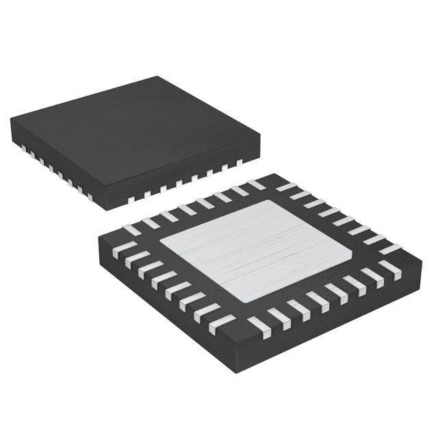
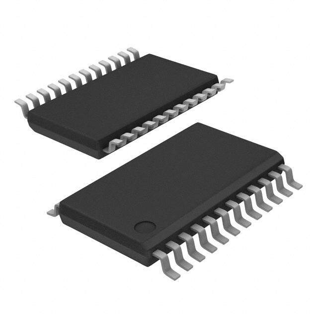
| 供应商器件封装 | 14-HTSSOP |
| 其它名称 | 296-24014-6 |
| 内部驱动器 | 是 |
| 包装 | Digi-Reel® |
| 单位重量 | 58 mg |
| 参考设计库 | http://www.digikey.com/rdl/4294959899/4294959898/455 |
| 商标 | Texas Instruments |
| 安装类型 | 表面贴装 |
| 安装风格 | SMD/SMT |
| 封装 | Reel |
| 封装/外壳 | 14-TSSOP (0.173",4.40mm 宽)裸焊盘 |
| 封装/箱体 | HTSSOP-14 |
| 工作温度 | -40°C ~ 85°C |
| 工作频率 | 2.2 MHz |
| 工厂包装数量 | 2000 |
| 恒压 | - |
| 恒流 | - |
| 拓扑 | PWM,升压(升压) |
| 拓扑结构 | Boost |
| 最大工作温度 | + 85 C |
| 最大电源电流 | 3.5 mA |
| 最小工作温度 | - 40 C |
| 标准包装 | 1 |
| 电压-电源 | 2.9 V ~ 18 V |
| 电压-输出 | 2.9 V ~ 38 V |
| 类型 | LED Driver |
| 类型-初级 | 背光,通用 |
| 类型-次级 | 高亮度 LED(HBLED),白色 LED |
| 系列 | TPS61500 |
| 输入电压 | 18 V |
| 输出数 | 1 |
| 输出电流 | 3 A |
| 输出端数量 | 1 Output |
| 输出类型 | Current Mode |
| 配用 | /product-detail/zh/TPS61500EVM-369/296-28552-ND/2232837 |
| 频率 | 200kHz ~ 2.2MHz |


- 商务部:美国ITC正式对集成电路等产品启动337调查
- 曝三星4nm工艺存在良率问题 高通将骁龙8 Gen1或转产台积电
- 太阳诱电将投资9.5亿元在常州建新厂生产MLCC 预计2023年完工
- 英特尔发布欧洲新工厂建设计划 深化IDM 2.0 战略
- 台积电先进制程称霸业界 有大客户加持明年业绩稳了
- 达到5530亿美元!SIA预计今年全球半导体销售额将创下新高
- 英特尔拟将自动驾驶子公司Mobileye上市 估值或超500亿美元
- 三星加码芯片和SET,合并消费电子和移动部门,撤换高东真等 CEO
- 三星电子宣布重大人事变动 还合并消费电子和移动部门
- 海关总署:前11个月进口集成电路产品价值2.52万亿元 增长14.8%


PDF Datasheet 数据手册内容提取
Product Order Technical Tools & Support & Folder Now Documents Software Community TPS61500 SLVS893F–DECEMBER2008–REVISEDMAY2019 TPS61500 High-Brightness, LED Driver With Integrated 3-A, 40-V Power Switch 1 Features The LED current is set with an external sensor resistor R3, and the feedback voltage that is • 2.9-Vto18-VInputVoltageRange 1 regulated to 200 mV by current mode PWM (pulse • 3-A,40-VInternalPowerSwitch width modulation) control loop, as shown in Typical – Four3-WLEDsFrom5-VInput Application Circuit. The device supports analog and pure PWM dimming methods for LED brightness – Eight3-WLEDsFrom12-VInput control. Connecting a capacitor to the DIMC pin • High-EfficiencyPowerConversion:Upto93% configures the device to be used for analog dimming, • FrequencySetbyExternalResistor:200kHzto and the LED current varies proportional to the duty 2.2MHz cycle of an external PWM signal. Floating the DIMC pin configures the device for pure PWM dimming with • User-DefinedSoftStartIntoFullLoad theaverageLED current being the PWM signal's duty • ProgrammableOvervoltageProtection cycletimesasetLEDcurrent. • AnalogandPurePWMBrightnessDimming The device features a programmable soft-start • 14-PinHTSSOPPackageWith PowerPAD™ function to limit inrush current during start-up, and it has other built-in protection features, such as pulse- 2 Applications by-pulse overcurrent limit, overvoltage protection, and thermal shutdown. The TPS61500 is available in 14- • MonitorBacklight pinHTSSOPpackagewithPowerPAD. • 1-Wor3-WHigh-BrightnessLED DeviceInformation(1) 3 Description PARTNUMBER PACKAGE BODYSIZE(NOM) The TPS61500 is a monolithic switching regulator TPS61500 HTSSOP(14) 5.00mm×4.40mm with integrated 3-A, 40-V power switch. It is an ideal driver for high brightness 1-W or 3-W LED. The (1) For all available packages, see the orderable addendum at theendofthedatasheet. device has a wide input voltage range to support application with input voltage from multi-cell batteries orregulated5-Vor12-Vpowerrails. TypicalApplicationCircuit Vin 5 V L1 D1 DL1 C1 3W LED C2 R1 TPS61500 VIN SW DL2 PWM EN SW R2 COMP OVP DL3 DIMC FB FREQ PGND DL4 C4 C5 SS PGND R4 C3 AGND PGND R3 1 An IMPORTANT NOTICE at the end of this data sheet addresses availability, warranty, changes, use in safety-critical applications, intellectualpropertymattersandotherimportantdisclaimers.PRODUCTIONDATA.
TPS61500 SLVS893F–DECEMBER2008–REVISEDMAY2019 www.ti.com Table of Contents 1 Features.................................................................. 1 7.4 DeviceFunctionalModes........................................11 2 Applications........................................................... 1 8 ApplicationandImplementation........................ 12 3 Description............................................................. 1 8.1 ApplicationInformation............................................12 4 RevisionHistory..................................................... 2 8.2 TypicalApplications................................................12 5 PinConfigurationandFunctions......................... 3 9 PowerSupplyRecommendations...................... 18 6 Specifications......................................................... 4 10 Layout................................................................... 18 6.1 AbsoluteMaximumRatings .....................................4 10.1 LayoutGuidelines.................................................18 6.2 ESDRatings..............................................................4 10.2 LayoutExample....................................................18 6.3 RecommendedOperatingConditions.......................4 10.3 ThermalConsiderations........................................19 6.4 ThermalInformation..................................................5 11 DeviceandDocumentationSupport................. 20 6.5 ElectricalCharacteristics...........................................5 11.1 DeviceSupport......................................................20 6.6 TypicalCharacteristics..............................................7 11.2 Trademarks...........................................................20 7 DetailedDescription.............................................. 9 11.3 ElectrostaticDischargeCaution............................20 7.1 Overview...................................................................9 11.4 Glossary................................................................20 7.2 FunctionalBlockDiagram.........................................9 12 Mechanical,Packaging,andOrderable Information........................................................... 20 7.3 FeatureDescription.................................................10 4 Revision History NOTE:Pagenumbersforpreviousrevisionsmaydifferfrompagenumbersinthecurrentversion. ChangesfromRevisionE(March2018)toRevisionF Page • Editorialchangesonly,notechnicalrevisions ....................................................................................................................... 1 ChangesfromRevisionD(June2017)toRevisionE Page • ChangedgroundsymbolofR3changefromPGNDtoAGNDinTypicalApplicationCircuit................................................ 1 • ChangedgroundsymbolofR3changefromPGNDtoAGNDinFigure7.......................................................................... 12 • ChangedgroundsymbolofR3changefromPGNDtoAGNDinFigure11........................................................................ 17 ChangesfromRevisionC(March2015)toRevisionD Page • Changed"AnalogandPWMdimmingfrequency"to"PWMdimmingfrequency"inROCtable;addseparaterowfor "Analogdimmingfrequency"................................................................................................................................................... 4 • AddedsentenceatendofAnalogDimmingMethod ........................................................................................................... 11 ChangesfromRevisionB(March2012)toRevisionC Page • AddedPinConfigurationandFunctionssection,ESDRatingstable,FeatureDescriptionsection,DeviceFunctional Modes,ApplicationandImplementationsection,PowerSupplyRecommendationssection,Layoutsection,Device andDocumentationSupportsection,andMechanical,Packaging,andOrderableInformationsection .............................. 1 ChangesfromRevisionA(February2012)toRevisionB Page • ChangedtheORDERINGINFORMATIONtablePACKAGEMARKINGFrom:TPS61500PWPTo:61500 ........................ 1 ChangesfromOriginal(December2008)toRevisionA Page • ReplacedtheDissipationRatingsTablewithThermalInformation........................................................................................ 4 2 SubmitDocumentationFeedback Copyright©2008–2019,TexasInstrumentsIncorporated ProductFolderLinks:TPS61500
TPS61500 www.ti.com SLVS893F–DECEMBER2008–REVISEDMAY2019 5 Pin Configuration and Functions PWPPackage 14-PinHTSSOPWithThermalPad TopView PinFunctions PIN I/O DESCRIPTION NAME NO. AGND 7 I SignalgroundoftheIC COMP 8 O Outputofthetransconductanceerroramplifier.AnexternalRCnetworkisconnectedtothispin. DIMC AnalogandPWMdimmingmethodoptionpin.Acapacitorconnectedtothepintosetthetimeconstant 6 I ofreferenceforanalogdimming.FloatthispinforPWMdimming. EN Enablepin.Whenthevoltageofthispinfallsbelowtheenablethresholdformorethan10ms,theIC 4 I turnsoff.ThispinisalsousedforPWMsignalinputforLEDbrightnessdimming. FB 9 I Feedbackpinforpositivevoltageregulation.AresistorconnectstothispintoprogramLEDcurrent. FREQ Switchfrequencyprogrampin.Anexternalresistorisconnectedtothispin.SeeApplicationInformation 10 O forinformationonhowtosizetheFREQresistor. OVP OvervoltageprotectionforLEDdriver.Thevoltageis1.229V.Usingaresistordividercanprogramthe 11 I thresholdofOVP. PGND 12-14 I PowergroundoftheIC.ItisconnectedtothesourceofthePWMswitch. SS Softstartprogrammingpin.AcapacitorbetweentheSSpinandGNDpinprogramssoft-starttiming.See 5 O ApplicationandImplementationforinformationonhowtosizetheSScapacitor SW 1,2 I ThisistheswitchingnodeoftheIC.ConnectSWtotheswitchedsideoftheinductor. ThermalPad Solderthethermalpadtotheanalogground.Ifpossible,usethermalviatoconnecttotopandinternal — — groundplanelayersforidealpowerdissipation. VIN TheinputpintotheIC.ConnectVINtoasupplyvoltagebetween2.9Vand18V.Itisacceptableforthe 3 I voltageonthepintobedifferentfromtheboostpowerstageinputforapplicationsrequiringvoltage beyondV range. IN Copyright©2008–2019,TexasInstrumentsIncorporated SubmitDocumentationFeedback 3 ProductFolderLinks:TPS61500
TPS61500 SLVS893F–DECEMBER2008–REVISEDMAY2019 www.ti.com 6 Specifications 6.1 Absolute Maximum Ratings overoperatingfree-airtemperaturerange(unlessotherwisenoted) (1) MIN MAX UNIT SupplyvoltagesonpinVIN(2) –0.3 20 V VoltagesonpinsEN(2) –0.3 20 V VoltageonpinFB,FREQandCOMP,OVP(2) –0.3 3 V VoltageonpinDIMC,SS(2) –0.3 7 V VoltageonpinSW(2) –0.3 40 V Continuouspowerdissipation SeeThermalInformation Operatingjunctiontemperature –40 150 °C Storagetemperature,T –65 150 °C stg (1) StressesbeyondthoselistedunderAbsoluteMaximumRatingsmaycausepermanentdamagetothedevice.Thesearestressratings onlyandfunctionaloperationofthedeviceattheseoranyotherconditionsbeyondthoseindicatedunderRecommendedOperating Conditionsisnotimplied.Exposuretoabsolute-maximum-ratedconditionsforextendedperiodsmayaffectdevicereliability. (2) Allvoltagevaluesarewithrespecttonetworkgroundterminal. 6.2 ESD Ratings VALUE UNIT Humanbodymodel(HBM),perANSI/ESDA/JEDECJS-001(1) ±2000 V Electrostaticdischarge V (ESD) Charged-devicemodel(CDM),perJEDECspecificationJESD22-C101(2) ±500 (1) JEDECdocumentJEP155statesthat500-VHBMallowssafemanufacturingwithastandardESDcontrolprocess. (2) JEDECdocumentJEP157statesthat250-VCDMallowssafemanufacturingwithastandardESDcontrolprocess. 6.3 Recommended Operating Conditions MIN NOM MAX UNIT V Inputvoltage 2.9 18 V IN V Outputvoltage V 38 V O IN L Inductor(1) 4.7 47 μH C Inputcapacitor 4.7 — μF I C Outputcapacitor 4.7 10 μF O Cdim Analogdimmingcapacitor(2) 0.1 — μF PWMdimmingfrequency(3) 200 1000 PWM Hz Analogdimmingfrequency(3) 200 40000 T Operatingambienttemperature –40 85 °C A T Operatingjunctiontemperature –40 125 °C J (1) Theinductancevaluedependsontheswitchingfrequencyandendapplications.Whilelargervaluesmaybeused,valuesbetween4.7 μHand47μHhavebeensuccessfullytestedinvariousapplications.RefertoSelectingtheInductorfordetails. (2) TheCdimwiththeinternalresistor(25kΩtypical)formsaRCfilterthatgeneratestheFBreferencevoltageaccordingtothedutycycle ofPWMsignal.TooptimizetheRCfilterandreducetheoutputripple,thevaluelargerthan0.1μFofCdimisrecommended. (3) Whenanalogdimming,themaximumPWMfrequencyissetbyontheRCfiltertooptimizetheoutputripple.WhenPWMdimming,the PWMfrequencyissetbythedeviceloopresponse. 4 SubmitDocumentationFeedback Copyright©2008–2019,TexasInstrumentsIncorporated ProductFolderLinks:TPS61500
TPS61500 www.ti.com SLVS893F–DECEMBER2008–REVISEDMAY2019 6.4 Thermal Information TPS61500 THERMALMETRIC(1) PWP(HTSSOP) UNIT 14PINS R Junction-to-ambientthermalresistance 45.2 °C/W θJA R Junction-to-case(top)thermalresistance 34.9 °C/W θJC(top) R Junction-to-boardthermalresistance 30.1 °C/W θJB ψ Junction-to-topcharacterizationparameter 1.5 °C/W JT ψ Junction-to-boardcharacterizationparameter 29.9 °C/W JB R Junction-to-case(bottom)thermalresistance 5.8 °C/W θJC(bot) (1) Formoreinformationabouttraditionalandnewthermalmetrics,seetheSemiconductorandICPackageThermalMetricsapplication report. 6.5 Electrical Characteristics FSW=1.2MHz(Rfreq=80kΩ),Vin=3.6V,CRTL=Vin,T =–40°Cto+85°C,typicalvaluesareatT =25°C(unless A A otherwisenoted) PARAMETER TESTCONDITIONS MIN TYP MAX UNIT SUPPLYCURRENT V Inputvoltagerange 2.9 18 V IN DevicePWMswitchingwithoutload,V = I OperatingquiescentcurrentintoVIN IN 3.5 mA Q 3.6V I Shutdowncurrent EN=GND,V =3.6V 1.5 μA SD IN V Undervoltagelockoutthreshold V falling 2.5 2.7 V UVLO IN V Undervoltagelockouthysteresis 130 mV hys ENABLEANDREFERENCECONTROL V ENlogichighvoltage V =2.9Vto18V 1.2 V enh IN V ENlogiclowvoltage V =2.9Vto18V 0.4 V enl IN R ENpulldownresistor 400 800 1600 kΩ en T Shutdowndelay,SSdischarge ENhightolow 10 ms off VOLTAGEANDCURRENTCONTROL V Voltagefeedbackregulationvoltage 195 200 205 mV REF I Voltagefeedbackinputbiascurrent 200 nA FB V Erroramplifieroffset –10 0 10 mV EA_OFF I COMPpinsinkcurrent V =V +200mV,V =1V 40 μA sink FB REF COMP I COMPpinsourcecurrent V =V –200mV,V =1V 40 μA source FB REF COMP Highclamp 3 V COMPpinclampvoltage V CCLP Lowclamp 0.75 V COMPpinthreshold Dutycycle=0% 0.95 V CTH G Erroramplifiertransconductance 240 340 440 μmho ea R Erroramplifieroutputresistance 10 MΩ ea f Erroramplifiercrossoverfrequency 500 kHz ea Copyright©2008–2019,TexasInstrumentsIncorporated SubmitDocumentationFeedback 5 ProductFolderLinks:TPS61500
TPS61500 SLVS893F–DECEMBER2008–REVISEDMAY2019 www.ti.com Electrical Characteristics (continued) FSW=1.2MHz(Rfreq=80kΩ),Vin=3.6V,CRTL=Vin,T =–40°Cto+85°C,typicalvaluesareatT =25°C(unless A A otherwisenoted) PARAMETER TESTCONDITIONS MIN TYP MAX UNIT FREQUENCY Rfreq=480kΩ 0.16 0.21 0.26 f Oscillatorfrequency Rfreq=80kΩ 1.0 1.2 1.4 MHz S Rfreq=40kΩ 1.76 2.2 2.64 D Maximumdutycycle Rfreq=80kΩ 89% 93% max V FREQpinvoltage 1.229 V FREQ T Minimumonpulsewidth Rfreq=80kΩ 60 ns min_on R Dimmingfilterresistance 25 kΩ dim_fil POWERSWITCH V =V =3.6V 0.13 0.25 IN GS R N-channelMOSFETon-resistance Ω DS(ON) V =V =3V 0.3 IN GS I N-channelleakagecurrent V =40V,T =25°C 1 μA LN_NFET DS A OC,OVPandSS I N-ChannelMOSFETcurrentlimit D=D 3 3.8 5 A LIM max I Soft-startbiascurrent Vss=0V 6 μA SS V Overvoltageprotectionthreshold 1.192 1.229 1.266 V OVP V Overvoltageprotectionhysteresis 40 mV OVP_hys THERMALSHUTDOWN T Thermalshutdownthreshold 160 °C shutdown Thermalshutdownthreshold T 15 °C hysteresis hysteresis 6 SubmitDocumentationFeedback Copyright©2008–2019,TexasInstrumentsIncorporated ProductFolderLinks:TPS61500
TPS61500 www.ti.com SLVS893F–DECEMBER2008–REVISEDMAY2019 6.6 Typical Characteristics Table1.TableofGraphs FIGURE Efficiency V =5V,4LEDs,8LEDs,10LEDs Figure1 IN Efficiency V =5V,12V;V =8LEDs Figure2 IN OUT FBvoltageaccuracy vsTemperature Figure3 Switchcurrentlimit vsDutycycle Figure4 Switchcurrentlimit vsTemperature Figure5 CircuitofTypicalApplicationCircuit;L1=D104C2-10μH;D1=SS3P6L-E3/86A,R4=80kΩ,C4=470nF,C2=10μF,LED =OSRAMLCWW5SM,I =400mA;unlessotherwisenoted. LED 100 100 VI= 5 V VI= 12 V 90 4 LEDs 90 8 LEDs VI= 5 V % 80 % 80 cy - 10 LEDs cy - n n e e Effici 70 Effici 70 8 LEDs 60 60 50 50 0 0.2 0.4 0.6 0.8 1 1.2 0 0.2 0.4 0.6 0.8 1 1.2 IO- Output Current -A IO- Output Current -A Figure1.Efficiency Figure2.Efficiency 210 5 205 4.5 A mV mit - Voltage - 200 urrent Li 4 FB verc O 195 3.5 190 3 -40 -20 0 20 40 60 80 100 120 0.2 0.4 0.6 0.8 1 TA- Free-Air Temperature - °C Duty Cycle - % Figure3.FBVoltageAccuracy Figure4.SwitchCurrentLimit Copyright©2008–2019,TexasInstrumentsIncorporated SubmitDocumentationFeedback 7 ProductFolderLinks:TPS61500
TPS61500 SLVS893F–DECEMBER2008–REVISEDMAY2019 www.ti.com CircuitofTypicalApplicationCircuit;L1=D104C2-10μH;D1=SS3P6L-E3/86A,R4=80kΩ,C4=470nF,C2=10μF,LED =OSRAMLCWW5SM,I =400mA;unlessotherwisenoted. LED 4 3.9 A mit - 3.8 Li nt e curr 3.7 er v O 3.6 3.5 -40 -20 0 20 40 60 80 100 120 TA- Free-Air Temperature - °C Figure5.SwitchCurrentLimit 8 SubmitDocumentationFeedback Copyright©2008–2019,TexasInstrumentsIncorporated ProductFolderLinks:TPS61500
TPS61500 www.ti.com SLVS893F–DECEMBER2008–REVISEDMAY2019 7 Detailed Description 7.1 Overview The TPS61500 integrates a 3-A, 40-V low side switch FET for driving up to 10 high-brightness LEDs in series. The device regulates the FB pin voltage at 200 mV with current mode pulse width modulation (PWM) control, andtheLEDcurrentissensedthroughalow-valueresistorinserieswithLEDs. The PWM control circuitry turns on the switch at the beginning of each switching cycle. The input voltage is applied across the inductor and stores the energy as inductor current ramps up. During this portion of the switching cycle, the load current is provided by the output capacitor. When the inductor current rises to the threshold set by the error amplifier output, the power switch turns off and the external Schottky diode is forward biased. The inductor transfers stored energy to replenish the output capacitor and supply the load current. This operation repeats each switching cycle. As shown in Functional Block Diagram, the duty cycle of the converter is determined by the PWM control comparator which compares the error amplifier output and the current signal. Theswitchingfrequencyisprogrammedbytheexternalresistor. A ramp signal from the oscillator is added to the current ramp. This slope compensation is necessary to avoid sub-harmonic oscillation that is intrinsic to the current mode control at duty cycle higher than 50%. The feedback loop regulates the FB pin to a reference voltage through an error amplifier. The output of the error amplifier is connected to the COMP pin. An external compensation network is connected to the COMP pin to optimize the feedbackloopforstabilityandtransientresponse. 7.2 Functional Block Diagram OVP VIN SW FB EA EN 1.229 V Ref. Gate Dirver 200 mV Ref. and DIMC Dimming COMP PWM Control Ramp Current + Generator Sensor Oscillator SS FREQ AGND PGND Copyright©2008–2019,TexasInstrumentsIncorporated SubmitDocumentationFeedback 9 ProductFolderLinks:TPS61500
TPS61500 SLVS893F–DECEMBER2008–REVISEDMAY2019 www.ti.com 7.3 Feature Description 7.3.1 SwitchingFrequency The switch frequency is determined by a resistor connected to the FREQ pin of the TPS61500. Do not leave this pin open. A resistor must always be connected for proper operation. See Table 2 and Figure 6 for resistor values andcorrespondingfrequencies. Table2.SwitchingFrequencyvsExternalResistor R4(kΩ) f (kHz) SW 443 240 256 400 176 600 80 1200 51 2000 3500 3000 2500 Hz k y - 2000 c n e qu 1500 e Fr f - 1000 500 0 10 100 1000 R4 - kW Figure6. SwitchingFrequencyvsExternalResistor Increasing switching frequency reduces the value of external capacitors and inductors, but also reduces the power conversion efficiency. The user must set the frequency for compromise between efficiency and solution size. 7.3.2 SoftStart The TPS61500 has a built-in soft-start circuit that significantly reduces the start-up current spike and output voltage overshoot. When the device is enabled, an internal bias current (typically 6 μA) charges a capacitor (C3) on the SS pin. The voltage at the capacitor clamps the output of the internal error amplifier that determines the duty cycle of PWM control, thereby the input inrush current is eliminated. Once the capacitor reaches 1.8 V, the soft-start cycle is completed, and the soft-start voltage no longer clamps the error amplifier output. Refer to Figure 14 and Figure 10 for the soft-start waveform. A 47-nF capacitor eliminates the output overshoot and reducesthepeakinductorcurrentformostapplications. When the EN is pulled low for 10 ms, the IC enters shutdown, and the SS capacitor discharges through a 5-kΩ resistorforthenextsoftstart. 7.3.3 EnableandThermalShutdown The TPS61500 enters shutdown when the EN voltage is less than 0.4 V for more than 10 ms. In shutdown, the input supply current for the device is less than 1.5 μA (maximum). The EN pin has an internal 800-kΩ pulldown resistortodisablethedevicewhenitisfloating. An internal thermal shutdown turns off the device when the typical junction temperature of 160°C is exceeded. Thedevicerestartswhenthejunctiontemperaturedropsby15°C. 10 SubmitDocumentationFeedback Copyright©2008–2019,TexasInstrumentsIncorporated ProductFolderLinks:TPS61500
TPS61500 www.ti.com SLVS893F–DECEMBER2008–REVISEDMAY2019 7.3.4 UndervoltageLockout(UVLO) An undervoltage lockout prevents mis-operation of the device at input voltages below typical 2.5 V. When the input voltage is below the undervoltage threshold, the device remains off and the internal switch FET is turned off. The undervoltage lockout threshold is set below minimum operating voltage of 2.9 V to avoid any transient VIN dip triggering the UVLO and causing the device to reset. For the input voltages between UVLO threshold and2.9V,thedevicemaintainsitsoperation,butthespecificationsarenotensured. 7.3.5 OvervoltageProtection When the FB pin is shorted to ground or an LED fails open circuit, the output voltage can increase to potentially damaging voltages. To present the device and the output capacitor from exceeding the maximum voltage rating, utilize the OVP pin with an external resistor divider to program an OVP threshold, as shown in the typical application. The OVP pin is set at 1.229 V, and the OVP threshold should be higher than the normal operating outputvoltage. 7.4 Device Functional Modes 7.4.1 PWMDimmingMethod LED brightness is controlled by peak LED current and duty cycle of external PWM signal. See Figure 11, Figure 12, and Figure 13, for the PWM dimming operating and linearity. Additional external switch FETs connect/disconnect LED string during PWM on/off period, shown in Figure 7. Simultaneously, the TPS61500 samples and holds the COMP voltage to speed up LED current regulation during the on period. Because the device and the external switch FETs must have several hundred microseconds to regulate the LED current, the frequency and minimum duty cycle of the PWM signal are application dependent. For example, 2% is the minimumdutycyclefora200-HzPWMsignal. The PWM dimming method offers better control of color because current through LED is kept constant each cycle. 7.4.2 AnalogDimmingMethod When capacitor C5 is connected to the DIMC pin, the FB regulation voltage is scaled proportional to the external PWM signal's duty cycle; therefore, it achieves LED brightness change, shown in Figure 7. The relationship betweenthedutycycleandLEDcurrentisgivenbyEquation1: V I = FB ´ Duty LED R3 where • DutyisthedutycycleofthePWMsignal. (1) The device chops up the internal 200-mV reference voltage at the duty cycle of the PWM signal. The pulsed reference voltage is then filtered by a low pass filter that is composed of an internal 25-kΩ resistor and the external capacitor C5. The output of the filter is connected to the error amplifier as the reference voltage for the FB pin. Therefore, although a PWM signal is used for brightness dimming, only the LED DC current is modulated. This eliminates the audible noise that often occurs when the LED current is pulsed during PWM dimming.UnlikeothermethodsforfilteringthePWMsignal, the device analog dimming method is independent of thePWMlogicvoltagelevelwhichoftenhaslargevariations. For optimum performance, TI recommends that the value of C5 be as large as possible to provide adequate filtering for the PWM frequency. For example, when the PWM frequency is 5-kHz, C5 equal to 1 μF is sufficient. The recommended minimum PWM on time at start-up is 200 µs. After start-up, TI recommends a minimum PWM dutycycleof1%. Copyright©2008–2019,TexasInstrumentsIncorporated SubmitDocumentationFeedback 11 ProductFolderLinks:TPS61500
TPS61500 SLVS893F–DECEMBER2008–REVISEDMAY2019 www.ti.com 8 Application and Implementation NOTE Information in the following applications sections is not part of the TI component specification, and TI does not warrant its accuracy or completeness. TI’s customers are responsible for determining suitability of components for their purposes. Customers should validateandtesttheirdesignimplementationtoconfirmsystemfunctionality. 8.1 Application Information The TPS61500 integrates a 3-A, 40-V low-side switch FET for driving up to 10 high brightness LEDs in series. The device regulates the FB pin voltage at 200 mV with current mode PWM control, and the LED current is sensed through a low value resistor in series with LEDs. The TPS61500 supports analog and pure PWM dimmingmethodsforLEDbrightnesscontrol.ConnectingacapacitortotheDIMC pin configures the device to be used for analog dimming, and the LED current varies proportional to the duty cycle of an external PWM signal. Floating the DIMC pin configures the device for pure PWM dimming with the average LED current being the PWMsignal'sdutycycletimesasetLEDcurrent. 8.2 Typical Applications 8.2.1 AnalogDimmingMethod Vin 5 V L1 D1 DL1 C1 3W LED C2 R1 TPS61500 VIN SW DL2 PWM EN SW R2 COMP OVP DL3 DIMC FB FREQ PGND DL4 C4 C5 SS PGND R4 C3 AGND PGND R3 Figure7. AnalogDimmingMethod 8.2.1.1 DesignRequirements Table3.DesignParameters PARAMETERS VALUES Inputvoltage 5V±20% LEDforwardvoltage 3.5V LEDcurrent 400mA NumberofLEDs 4 Dimmingmethod Analog 12 SubmitDocumentationFeedback Copyright©2008–2019,TexasInstrumentsIncorporated ProductFolderLinks:TPS61500
TPS61500 www.ti.com SLVS893F–DECEMBER2008–REVISEDMAY2019 8.2.1.2 DetailedDesignProcedure 8.2.1.2.1 ProgrammingtheOvervoltageProtection SelectthevaluesofR1andR2accordingtoEquation2. æR1 ö V =1.229V ´ +1 OVP çèR2 ÷ø (2) For example, the total forward voltage of four 3-W LED is 14V, then use R1 of 120 k and R2 of 10 k to program thethresholdof16V.IntheOVPmode,thedeviceregulatestheoutputvoltageattheOVPthreshold. When the fault is clear and the OVP pin voltage falls 40 mV below 1.229 V, IC resumes the output regulation for LEDcurrent. 8.2.1.2.2 ProgrammingtheLEDCurrent LEDcurrentcanbedeterminedby the value of the feedback resistor R3 and the FB pin regulation voltage of 200 mVasshowninEquation3: V I = FB LED R3 (3) TheoutputcurrenttolerancedependsontheFBaccuracyandthecurrentsensorresistoraccuracy. 8.2.1.2.3 ImplementingDimming TheTPS61500providestwoLEDcurrentdimmingmethods. • FloatingtheDIMCpin,anexternalPWMsignalviatheENpin,providingpurePWMdimmingmethod. • Connecting a capacitor larger than 100-nF to the DIMC pin, an external PWM signal via the EN pin, providing analogdimming.Inthisapplication,a1-µFcapacitorisconnectedtotheDIMCpin. 8.2.1.2.4 ComputingtheMaximumOutputCurrent The overcurrent limit in a boost converter limits the maximum input current and thus maximum input power for a given input voltage. Maximum output power is less than maximum input power due to power conversion losses. Therefore, the current limit setting, input voltage, output voltage and efficiency can all change maximum current output. The current limit clamps the peak inductor current; therefore, the ripple has to be subtracted to derive maximum DC current. The ripple current is a function of switching frequency, inductor value and duty cycle. Equation4andEquation5takeintoaccountofalltheabovefactorsformaximumoutputcurrentcalculation. 1 I = p é æ 1 1 öù êL ´ Fs ´ ç + ÷ú ë èVout+V¦ - Vin Vinøû where • I =inductorpeak-to-peakripple p • L=inductorvalue • Vƒ=Schottkydiodeforwardvoltage • Fs=switchingfrequency • V =outputvoltage=ΣV +V (4) out LEDs REF Vin× (I - I /2) ´ h lim p I = LED_max Vout where • I =maximumLEDcurrentfromtheboostconverter LED_max • I =overcurrentlimit lim • V =LEDforwardvoltageatI LED LED • η=efficiencyestimatebasedonsimilarapplications (5) For instance, when V is 12 V, 8 LEDs output is equivalent to V of 24 V, the inductor is 10 μH, the Schottky IN OUT forward voltage is 0.4 V, and the switching frequency is 1.2 MHz; then the maximum output current is approximately1Aintypicalcondition. Copyright©2008–2019,TexasInstrumentsIncorporated SubmitDocumentationFeedback 13 ProductFolderLinks:TPS61500
TPS61500 SLVS893F–DECEMBER2008–REVISEDMAY2019 www.ti.com 8.2.1.2.5 SelectingtheInductor Theselection of the inductor affects steady state operation as well as transient behavior and loop stability. These factors make it the most important component in power regulator design. There are three important inductor specifications, inductor value, DC resistance, and saturation current. Considering inductor value alone is not enough. Inductor values can have ±20% tolerance with no current bias. When the inductor current approaches saturation level, its inductance can falls to some percentage of its 0-A value depending on how the inductor vendor defines saturationcurrent. Using an inductor with a smaller inductance value forces discontinuous PWM where the inductor current ramps down to zero before the end of each switching cycle. This reduces the maximum output current of the boost converter, causes large input voltage ripple and reduces efficiency. In general, large inductance value provides much more output and higher conversion efficiency. Small inductance value can give better the load transient response. For these reasons, TI recommends a 4.7-μH to 22-μH inductor value range. Table 4 lists the recommendedinductorfortheTPS61500. Meanwhile, the TPS61500 can program the switching frequency. Normally, small inductance value is suitable for high frequency and vice versa. The device has built-in slope compensation to avoid sub-harmonic oscillation associated with current mode control. If the inductor value is lower than 4.7 μH, the slope compensation may not be adequate, and the loop can be unstable. Therefore, customers should verify the inductor in their application if itisdifferentfromtherecommendedvalues. Table4.RecommendedInductorsforTPS61500 PARTNUMBER L(µH) DCRMAX(mΩ) SATURATIONCURRENT(A) SIZE(L×W×Hmm) VENDOR(1) D104C2 10 44 3.6 10.4×10.4×4.8 TOKO VLF10040 15 42 3.1 10.0×9.7×4.0 TDK CDRH105RNP 22 61 2.9 10.5×10.3×5.1 Sumida MSS1038 15 50 3.8 10.0×10.2×3.8 Coilcraft (1) SeeThird-PartyProductsdisclaimer. 8.2.1.2.6 SelectingtheSchottkyDiode The high switching frequency of the TPS61500 demands a high-speed rectification for optimum efficiency. Ensure that the diode’s average and peak current rating exceed the average output current and peak inductor current. In addition, reverse breakdown voltage of the diode must exceed the switch FET rating voltage of 40 V. TI recommends the VISHAY SS3P6L-E3/86A the TPS61500 device. The power dissipation of the diode package mustbelargerthantheI ×V OUT(max) D 8.2.1.2.7 SelectingtheCompensationCapacitorandResistor The TPS61500 has an external compensation, COMP pin, which allows the loop response to be optimized for each application. The COMP pin is the output of the internal error amplifier. An external ceramic capacitor, C4, is connectedtotheCOMPpintostabilizethefeedbackloop.Use470nFforC4. 8.2.1.2.8 SelectingtheInputandOutputCapacitor The output capacitor is selected mainly to meet the requirements for the output ripple and loop stability. This ripple voltage is related to the capacitor capacitance and its equivalent series resistance (ESR). Assuming a capacitorwithzeroESR,theminimumcapacitanceneededforagivenripplecanbecalculatedby (V - V )I out in out C = out V ´ Fs ´ V out ripple where • V =peak-to-peakoutputripple (6) ripple TheadditionaloutputripplecomponentcausedbyESRiscalculatedusing: V =I ´ R ripple_ESR out ESR (7) 14 SubmitDocumentationFeedback Copyright©2008–2019,TexasInstrumentsIncorporated ProductFolderLinks:TPS61500
TPS61500 www.ti.com SLVS893F–DECEMBER2008–REVISEDMAY2019 Due to its low ESR, V can be neglected for ceramic capacitors, but must be considered if tantalum or ripple_ESR electrolyticcapacitorsareused. Take care when evaluating a ceramic capacitor’s derating under DC bias, aging and AC signal. For example, larger form factor capacitors (in 1206 size) have their self-resonant frequencies in the range of the switching frequency; thus, the effective capacitance is significantly lower. The DC bias can also significantly reduce capacitance. Ceramic capacitors can loss as much as 50% of its capacitance at its rated voltage. Therefore, leavemarginonthevoltageratingtoensureadequatecapacitanceattherequiredoutputvoltage. TI recommends a capacitor in the range of 1 µF to 4.7 μF for input side. The output requires a capacitor in the range of 1 μF to 10 μF. The output capacitor affects the loop stability of the boost regulator. If the output capacitorisbelowtherange,theboostregulatorcanpotentiallybecomeunstable. Thepopularvendorsforhigh-valueceramiccapacitorsare: • TDK(http://www.component.tdk.com/components.php) • Murata(http://www.murata.com/cap/index.html) Copyright©2008–2019,TexasInstrumentsIncorporated SubmitDocumentationFeedback 15 ProductFolderLinks:TPS61500
TPS61500 SLVS893F–DECEMBER2008–REVISEDMAY2019 www.ti.com 8.2.1.3 ApplicationCurves 210 PWM Frequency EN 180 200 Hz, 5 kHz, 40 kHz 5 V/div 150 V VOUT m 50 mV/AdiCv ge - 120 a olt V 90 B F 60 ILED 100 mA/div 30 0 t - 200ms/div 0 20 40 60 80 100 Duty Cycle - % Figure8.AnalogDimming Figure9.AnalogDimmingLinearity EN 5 V/div VOUT 5 V/div IL 500 mA/div t - 4 ms/div Figure10.AnalogDimmingStart-up 8.2.2 PurePWMDimmingMethod D1 Vin 5 V L1 Q2 DL1 C1 1k 3W LED TPS61500 R1 VIN SW C2 DL2 PWM 1k EN SW R2 COMP OVP DL3 Q1 DIMC FB PWM FREQ PGND DL4 C4 SS PGND R4 C3 AGND PGND R3 Figure11. PurePWMDimmingMethod 16 SubmitDocumentationFeedback Copyright©2008–2019,TexasInstrumentsIncorporated ProductFolderLinks:TPS61500
TPS61500 www.ti.com SLVS893F–DECEMBER2008–REVISEDMAY2019 8.2.2.1 DesignRequirements Table5.DesignParameters PARAMETERS VALUES Inputvoltage 5V±20% LEDforwardvoltage 3.5V LEDcurrent 400mA NumberofLEDs 4 Dimmingmethod PWM 8.2.2.2 DetailedDesignProcedure RefertoDetailedDesignProcedureintheAnalogDimmingMethodsection. 8.2.2.3 ApplicationCurves 450 PWM Frequency 400 200 Hz, 600 Hz, 1000 Hz EN 5 V/div 350 300 A m VOUT nt - 250 200 mV/AdiCv urre200 C D E150 L 100 ILED 500 mA/div 50 0 0 20 40 60 80 100 t - 200 ms/div Duty Cycle - % Figure12.PWMDimming Figure13.PWMDimmingLinearity EN 5 V/div VOUT 5 V/div ILED 500 mA/div t - 4 ms/div Figure14.PWMDimmingStart-up Copyright©2008–2019,TexasInstrumentsIncorporated SubmitDocumentationFeedback 17 ProductFolderLinks:TPS61500
TPS61500 SLVS893F–DECEMBER2008–REVISEDMAY2019 www.ti.com 9 Power Supply Recommendations The TPS61500 is designed to operate from an input voltage supply range between 2.9 V and 18 V. The power supply to the TPS61500 must have a current rating according to the supply voltage, output voltage, and output currentoftheTPS61500. 10 Layout 10.1 Layout Guidelines As for all switching power supplies, especially those running at high switching frequency and high currents, layout is an important design step. If layout is not carefully done, the regulator could suffer from instability as well as noise problems. To maximize efficiency, switch rise and fall times are very fast. To prevent radiation of high frequency noise (for example, EMI), proper layout of the high frequency switching path is essential. Minimize the length and area of all traces connected to the SW pin and always use a ground plane under the switching regulator to minimize interplane coupling. The high current path including the switch, Schottky diode, and output capacitor, contains nanosecond rise and fall times and must be kept as short as possible. In order to reduce the inputsupplyripple,theinputcapacitormustbeclosebothtotheVINandGNDpins. 10.2 Layout Example VIN INPUT CAPACITOR VOUT INDUCTOR SCHOTTKEY OUTPUT CAPACITOR SW LED String SW PGND Minimize the area of SW trace SW PGND PGND VIN PGND T h e EN rm OVP a l P a SS d FREQ DMIC FB FEEDBACK AGND COMP COMPENSATION Place enough AGND VIAs around thermal pad to enhance thermal performance Figure15. RecommendedLayoutExample 18 SubmitDocumentationFeedback Copyright©2008–2019,TexasInstrumentsIncorporated ProductFolderLinks:TPS61500
TPS61500 www.ti.com SLVS893F–DECEMBER2008–REVISEDMAY2019 10.3 Thermal Considerations As mentioned before, the maximum device junction temperature must be restricted to 125°C under normal operating conditions. This restriction limits the power dissipation of the TPS61500. Calculate the maximum allowable dissipation, P (maximum), and keep the actual dissipation less than or equal to P (maximum). The D D maximum-power-dissipationlimitisdeterminedusingEquation8: 125°C - T A P = D(max) R θJA where • T isthemaximumambienttemperaturefortheapplication A • R isthethermalresistancejunction-to-ambientgiveninThermalInformation (8) θJA The TPS61500 comes in a thermally enhanced TSSOP package. This package includes a thermal pad that improves the thermal capabilities of the package. The R of the TSSOP package greatly depends on the PCB θJA layout. Copyright©2008–2019,TexasInstrumentsIncorporated SubmitDocumentationFeedback 19 ProductFolderLinks:TPS61500
TPS61500 SLVS893F–DECEMBER2008–REVISEDMAY2019 www.ti.com 11 Device and Documentation Support 11.1 Device Support 11.1.1 Third-PartyProductsDisclaimer TI'S PUBLICATION OF INFORMATION REGARDING THIRD-PARTY PRODUCTS OR SERVICES DOES NOT CONSTITUTE AN ENDORSEMENT REGARDING THE SUITABILITY OF SUCH PRODUCTS OR SERVICES OR A WARRANTY, REPRESENTATION OR ENDORSEMENT OF SUCH PRODUCTS OR SERVICES, EITHER ALONEORINCOMBINATIONWITHANYTIPRODUCTORSERVICE. 11.1.2 ReceivingNotificationofDocumentationUpdates To receive notification of documentation updates, navigate to the device product folder on ti.com. In the upper right corner, click on Alert me to register and receive a weekly digest of any product information that has changed.Forchangedetails,reviewtherevisionhistoryincludedinanyreviseddocument. 11.1.3 CommunityResources The following links connect to TI community resources. Linked contents are provided "AS IS" by the respective contributors. They do not constitute TI specifications and do not necessarily reflect TI's views; see TI's Terms of Use. TIE2E™OnlineCommunity TI'sEngineer-to-Engineer(E2E)Community.Createdtofostercollaboration amongengineers.Ate2e.ti.com,youcanaskquestions,shareknowledge,exploreideasandhelp solveproblemswithfellowengineers. DesignSupport TI'sDesignSupport QuicklyfindhelpfulE2Eforumsalongwithdesignsupporttoolsand contactinformationfortechnicalsupport. 11.2 Trademarks PowerPAD,E2EaretrademarksofTexasInstruments. Allothertrademarksarethepropertyoftheirrespectiveowners. 11.3 Electrostatic Discharge Caution Thesedeviceshavelimitedbuilt-inESDprotection.Theleadsshouldbeshortedtogetherorthedeviceplacedinconductivefoam duringstorageorhandlingtopreventelectrostaticdamagetotheMOSgates. 11.4 Glossary SLYZ022—TIGlossary. Thisglossarylistsandexplainsterms,acronyms,anddefinitions. 12 Mechanical, Packaging, and Orderable Information The following pages include mechanical, packaging, and orderable information. This information is the most current data available for the designated devices. This data is subject to change without notice and revision of thisdocument.Forbrowser-basedversionsofthisdatasheet,refertotheleft-handnavigation. 20 SubmitDocumentationFeedback Copyright©2008–2019,TexasInstrumentsIncorporated ProductFolderLinks:TPS61500
PACKAGE OPTION ADDENDUM www.ti.com 6-Feb-2020 PACKAGING INFORMATION Orderable Device Status Package Type Package Pins Package Eco Plan Lead/Ball Finish MSL Peak Temp Op Temp (°C) Device Marking Samples (1) Drawing Qty (2) (6) (3) (4/5) TPS61500PWP ACTIVE HTSSOP PWP 14 90 Green (RoHS NIPDAU Level-2-260C-1 YEAR -40 to 85 61500 & no Sb/Br) TPS61500PWPR ACTIVE HTSSOP PWP 14 2000 Green (RoHS NIPDAU Level-2-260C-1 YEAR -40 to 85 61500 & no Sb/Br) (1) The marketing status values are defined as follows: ACTIVE: Product device recommended for new designs. LIFEBUY: TI has announced that the device will be discontinued, and a lifetime-buy period is in effect. NRND: Not recommended for new designs. Device is in production to support existing customers, but TI does not recommend using this part in a new design. PREVIEW: Device has been announced but is not in production. Samples may or may not be available. OBSOLETE: TI has discontinued the production of the device. (2) RoHS: TI defines "RoHS" to mean semiconductor products that are compliant with the current EU RoHS requirements for all 10 RoHS substances, including the requirement that RoHS substance do not exceed 0.1% by weight in homogeneous materials. Where designed to be soldered at high temperatures, "RoHS" products are suitable for use in specified lead-free processes. TI may reference these types of products as "Pb-Free". RoHS Exempt: TI defines "RoHS Exempt" to mean products that contain lead but are compliant with EU RoHS pursuant to a specific EU RoHS exemption. Green: TI defines "Green" to mean the content of Chlorine (Cl) and Bromine (Br) based flame retardants meet JS709B low halogen requirements of <=1000ppm threshold. Antimony trioxide based flame retardants must also meet the <=1000ppm threshold requirement. (3) MSL, Peak Temp. - The Moisture Sensitivity Level rating according to the JEDEC industry standard classifications, and peak solder temperature. (4) There may be additional marking, which relates to the logo, the lot trace code information, or the environmental category on the device. (5) Multiple Device Markings will be inside parentheses. Only one Device Marking contained in parentheses and separated by a "~" will appear on a device. If a line is indented then it is a continuation of the previous line and the two combined represent the entire Device Marking for that device. (6) Lead/Ball Finish - Orderable Devices may have multiple material finish options. Finish options are separated by a vertical ruled line. Lead/Ball Finish values may wrap to two lines if the finish value exceeds the maximum column width. Important Information and Disclaimer:The information provided on this page represents TI's knowledge and belief as of the date that it is provided. TI bases its knowledge and belief on information provided by third parties, and makes no representation or warranty as to the accuracy of such information. Efforts are underway to better integrate information from third parties. TI has taken and continues to take reasonable steps to provide representative and accurate information but may not have conducted destructive testing or chemical analysis on incoming materials and chemicals. TI and TI suppliers consider certain information to be proprietary, and thus CAS numbers and other limited information may not be available for release. In no event shall TI's liability arising out of such information exceed the total purchase price of the TI part(s) at issue in this document sold by TI to Customer on an annual basis. Addendum-Page 1
PACKAGE OPTION ADDENDUM www.ti.com 6-Feb-2020 Addendum-Page 2
PACKAGE MATERIALS INFORMATION www.ti.com 30-May-2019 TAPE AND REEL INFORMATION *Alldimensionsarenominal Device Package Package Pins SPQ Reel Reel A0 B0 K0 P1 W Pin1 Type Drawing Diameter Width (mm) (mm) (mm) (mm) (mm) Quadrant (mm) W1(mm) TPS61500PWPR HTSSOP PWP 14 2000 330.0 12.4 6.9 5.6 1.6 8.0 12.0 Q1 PackMaterials-Page1
PACKAGE MATERIALS INFORMATION www.ti.com 30-May-2019 *Alldimensionsarenominal Device PackageType PackageDrawing Pins SPQ Length(mm) Width(mm) Height(mm) TPS61500PWPR HTSSOP PWP 14 2000 350.0 350.0 43.0 PackMaterials-Page2
None
None
None
None
None
IMPORTANTNOTICEANDDISCLAIMER TI PROVIDES TECHNICAL AND RELIABILITY DATA (INCLUDING DATASHEETS), DESIGN RESOURCES (INCLUDING REFERENCE DESIGNS), APPLICATION OR OTHER DESIGN ADVICE, WEB TOOLS, SAFETY INFORMATION, AND OTHER RESOURCES “AS IS” AND WITH ALL FAULTS, AND DISCLAIMS ALL WARRANTIES, EXPRESS AND IMPLIED, INCLUDING WITHOUT LIMITATION ANY IMPLIED WARRANTIES OF MERCHANTABILITY, FITNESS FOR A PARTICULAR PURPOSE OR NON-INFRINGEMENT OF THIRD PARTY INTELLECTUAL PROPERTY RIGHTS. These resources are intended for skilled developers designing with TI products. You are solely responsible for (1) selecting the appropriate TI products for your application, (2) designing, validating and testing your application, and (3) ensuring your application meets applicable standards, and any other safety, security, or other requirements. These resources are subject to change without notice. TI grants you permission to use these resources only for development of an application that uses the TI products described in the resource. Other reproduction and display of these resources is prohibited. No license is granted to any other TI intellectual property right or to any third party intellectual property right. TI disclaims responsibility for, and you will fully indemnify TI and its representatives against, any claims, damages, costs, losses, and liabilities arising out of your use of these resources. TI’s products are provided subject to TI’s Terms of Sale (www.ti.com/legal/termsofsale.html) or other applicable terms available either on ti.com or provided in conjunction with such TI products. TI’s provision of these resources does not expand or otherwise alter TI’s applicable warranties or warranty disclaimers for TI products. Mailing Address: Texas Instruments, Post Office Box 655303, Dallas, Texas 75265 Copyright © 2020, Texas Instruments Incorporated