ICGOO在线商城 > 集成电路(IC) > PMIC - 稳压器 - DC DC 开关稳压器 > TPS61240YFFR
 Datasheet下载
- 型号: TPS61240YFFR
- 制造商: Texas Instruments
- 库位|库存: xxxx|xxxx
- 要求:
| 数量阶梯 | 香港交货 | 国内含税 |
| +xxxx | $xxxx | ¥xxxx |
查看当月历史价格
查看今年历史价格
TPS61240YFFR产品简介:
ICGOO电子元器件商城为您提供TPS61240YFFR由Texas Instruments设计生产,在icgoo商城现货销售,并且可以通过原厂、代理商等渠道进行代购。 TPS61240YFFR价格参考。Texas InstrumentsTPS61240YFFR封装/规格:PMIC - 稳压器 - DC DC 开关稳压器, 固定 升压 开关稳压器 IC 正 5V 1 输出 500mA(开关) 6-UFBGA,DSBGA。您可以下载TPS61240YFFR参考资料、Datasheet数据手册功能说明书,资料中有TPS61240YFFR 详细功能的应用电路图电压和使用方法及教程。
TPS61240YFFR 是 Texas Instruments(德州仪器)推出的一款高效升压 DC-DC 开关稳压器,属于 PMIC(电源管理集成电路)类别。该型号具有低功耗、高效率和小尺寸的特点,适用于多种便携式电子设备和电池供电系统。以下是其主要应用场景:

 1. 便携式电子产品
   - TPS61240YFFR 的高效升压特性使其非常适合为便携式设备供电,例如:
     - 移动电源
     - 蓝牙耳机
     - 智能手环/智能手表
     - 便携式音频设备(如扬声器和 MP3 播放器)
   - 它能够将单节锂离子电池(2.7V 至 5.5V 输入范围)的电压提升至更高的输出电压,从而为负载提供稳定电源。

 2. 无线通信设备
   - 在物联网(IoT)设备和无线传感器网络中,TPS61240YFFR 可用于为射频模块(如蓝牙、Wi-Fi 和 Zigbee)供电。
   - 其低静态电流(典型值为 25µA)有助于延长电池寿命,特别适合需要长时间运行的低功耗应用。

 3. 消费类电子设备
   - 该芯片适用于需要升压功能的消费类电子产品,例如:
     - 数码相机
     - 电子阅读器
     - 游戏控制器
   - 其高达 1A 的输出电流能力可满足这些设备对功率的需求。

 4. 工业应用
   - 在工业领域,TPS61240YFFR 可用于为远程传感器、数据采集模块和小型控制单元供电。
   - 它的小型封装(WSON-10 封装)和高集成度使得其在空间受限的工业设计中非常实用。

 5. 医疗设备
   - 该稳压器可用于便携式医疗设备,例如:
     - 血糖仪
     - 脉搏血氧仪
     - 可穿戴健康监测设备
   - 其高效率和低噪声性能确保了设备的精确测量和长续航时间。

 6. 汽车电子配件
   - 在汽车后装市场中,TPS61240YFFR 可用于为行车记录仪、倒车摄像头等设备供电。
   - 其宽输入电压范围和过流保护功能增强了系统的可靠性和安全性。

 总结
TPS61240YFFR 凭借其高效的升压转换能力、紧凑的设计和广泛的输入电压范围,成为便携式设备、无线通信、消费类电子、工业应用和医疗设备的理想选择。它能够在保证高性能的同时,帮助设计师优化系统功耗和成本。
| 参数 | 数值 |
| 产品目录 | 集成电路 (IC)半导体 |
| 描述 | IC REG BST SYNC 5V 0.45A 6DSBGA稳压器—开关式稳压器 5V, 400mA, 4MHz Step Up DC/DC Converter |
| DevelopmentKit | TPS61240EVM-360 |
| 产品分类 | |
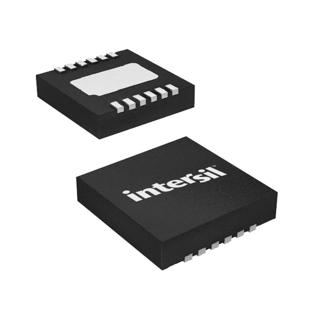
| 品牌 | Texas Instruments |
| 产品手册 | http://www.ti.com/litv/slvs806b |
| 产品图片 |
|
| rohs | 符合RoHS无铅 / 符合限制有害物质指令(RoHS)规范要求 |
| 产品系列 | 电源管理 IC,稳压器—开关式稳压器,Texas Instruments TPS61240YFFR- |
| 数据手册 | |
| 产品型号 | TPS61240YFFR |
| PWM类型 | 电流模式 |
| 产品目录页面 | |
| 产品种类 | 稳压器—开关式稳压器 |
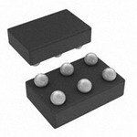
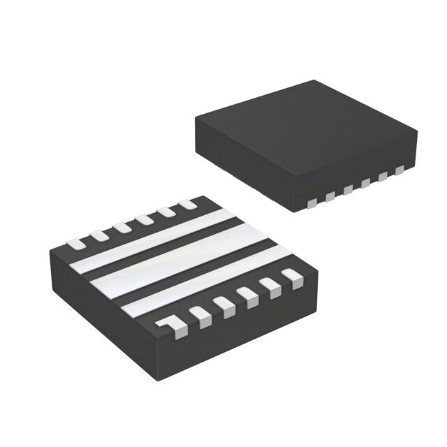
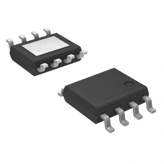
| 供应商器件封装 | 6-DSBGA |
| 关闭 | Shutdown |
| 其它名称 | 296-24409-1 |
| 包装 | 剪切带 (CT) |
| 同步整流器 | 是 |
| 商标 | Texas Instruments |
| 安装类型 | 表面贴装 |
| 安装风格 | SMD/SMT |
| 封装 | Reel |
| 封装/外壳 | 6-UFBGA,DSBGA |
| 封装/箱体 | DSBGA-6 |
| 工作温度 | -40°C ~ 85°C |
| 工作温度范围 | - 40 C to + 85 C |
| 工厂包装数量 | 3000 |
| 开关频率 | 3.5 MHz |
| 拓扑结构 | Boost |
| 最大工作温度 | + 85 C |
| 最大输入电压 | 5.5 V |
| 最小工作温度 | - 40 C |
| 最小输入电压 | 2.3 V |
| 标准包装 | 1 |
| 电压-输入 | 2.3 V ~ 5.5 V |
| 电压-输出 | 5V |
| 电流-输出 | 450mA |
| 电源电压-最小 | 2.3 V |
| 电源电流 | 30 uA |
| 类型 | 升压(升压) |
| 系列 | TPS61240 |
| 输入电压 | 2.3 V to 5.5 V |
| 输出数 | 1 |
| 输出电压 | 5 V |
| 输出电流 | 450 mA |
| 输出端数量 | 1 Output |
| 输出类型 | 固定 |
| 配用 | /product-detail/zh/TPS61240EVM-360/296-31240-ND/2232835 |
| 频率-开关 | 3.5MHz |


- 商务部:美国ITC正式对集成电路等产品启动337调查
- 曝三星4nm工艺存在良率问题 高通将骁龙8 Gen1或转产台积电
- 太阳诱电将投资9.5亿元在常州建新厂生产MLCC 预计2023年完工
- 英特尔发布欧洲新工厂建设计划 深化IDM 2.0 战略
- 台积电先进制程称霸业界 有大客户加持明年业绩稳了
- 达到5530亿美元!SIA预计今年全球半导体销售额将创下新高
- 英特尔拟将自动驾驶子公司Mobileye上市 估值或超500亿美元
- 三星加码芯片和SET,合并消费电子和移动部门,撤换高东真等 CEO
- 三星电子宣布重大人事变动 还合并消费电子和移动部门
- 海关总署:前11个月进口集成电路产品价值2.52万亿元 增长14.8%


PDF Datasheet 数据手册内容提取
Product Sample & Technical Tools & Support & Folder Buy Documents Software Community TPS61240,TPS61241 SLVS806D–APRIL2009–REVISEDDECEMBER2015 TPS6124x 3.5-MHz High Efficiency Step-Up Converter 1 Features 3 Description • Efficiency> 90%atNominalOperatingConditions The TPS6124x device is a highly efficient 1 synchronous step-up DC-DC converter optimized for • TotalDCOutputVoltageAccuracy5.0V±2% products powered by either a three-cell alkaline, NiCd • Typical30-μAQuiescentCurrent or NiMH, or one-cell Li-Ion or Li-Polymer battery. The • BestinClassLineandLoadTransient TPS6124x supports output currents up to 450 mA. TheTPS61240hasaninputvalleycurrentlimitof500 • WideV RangeFrom2.3Vto5.5V IN mA, and the TPS61241 has an input valley current of • OutputCurrentupto450mA 600mA. • AutomaticPFM/PWMModeTransition With an input voltage range of 2.3 V to 5.5 V, the • LowRipplePowerSaveModeforImproved device supports batteries with extended voltage EfficiencyatLightLoads range and are ideal to power portable applications • InternalSoftstart,250-μsTypicalStart-UpTime like mobile phones and other portable equipment. The TPS6124x boost converter is based on a quasi- • 3.5-MHzTypicalOperatingFrequency constanton-timevalleycurrentmodecontrolscheme. • LoadDisconnectDuringShutdown The TPS6124x presents a high impedance at the • CurrentOverloadandThermalShutdown V pin when shut down. This allows for use in Protection OUT applications that require the regulated output bus to • ThreeSurface-MountExternalComponents be driven by another supply while the TPS6124x is Required(OneMLCCInductor,TwoCeramic shutdown. Capacitors) During light loads the device will automatically pulse • TotalSolutionSize <13mm2 skip allowing maximum efficiency at lowest quiescent • Availableina6-PinDSBGAand2-mm× 2-mm currents. In the shutdown mode, the current WSONPackage consumptionisreducedtolessthan1μA. TPS6124x allows the use of small inductors and 2 Applications capacitors to achieve a small solution size. During shutdown, the load is completely disconnected from • USB-OTGApplications the battery. The TPS6124x is available in a 6-pin • PortableHDMIApplications DSBGAand2-mm×2-mmWSONpackage. • CellPhones,SmartPhones • PDAs,PocketPCs DeviceInformation(1) • PortableMediaPlayers PARTNUMBER PACKAGE BODYSIZE(NOM) • DigitalCameras WSON(6) 2.00mm×2.00mm TPS61240 DSBGA(6) 1.25mm×0.86mm TPS61241 DSBGA(6) 1.25mm×0.86mm (1) For all available packages, see the orderable addendum at theendofthedatasheet. TypicalApplicationSchematic EfficiencyvsOutputCurrent TPS61240 L 100 V 1mH L VOUT COUT VOUT5 V 90 VI= 3.6 V VI= 4.2 V IN VIN FB 4.7mF 80 C 70 VI= 3 V IN 2.2mF EN GND Efficiency - % 456000 VI= 2.3 V 30 20 10 0 0.00001 0.0001 0.001 0.01 0.1 1 IO- Output Current -A 1 An IMPORTANT NOTICE at the end of this data sheet addresses availability, warranty, changes, use in safety-critical applications, intellectualpropertymattersandotherimportantdisclaimers.PRODUCTIONDATA.
TPS61240,TPS61241 SLVS806D–APRIL2009–REVISEDDECEMBER2015 www.ti.com Table of Contents 1 Features.................................................................. 1 9.4 DeviceFunctionalModes........................................11 2 Applications........................................................... 1 10 ApplicationandImplementation........................ 12 3 Description............................................................. 1 10.1 ApplicationInformation..........................................12 4 RevisionHistory..................................................... 2 10.2 TypicalApplication ...............................................12 10.3 SystemExamples.................................................17 5 DeviceOptions....................................................... 3 11 PowerSupplyRecommendations..................... 17 6 PinConfigurationandFunctions......................... 3 12 Layout................................................................... 18 7 Specifications......................................................... 4 12.1 LayoutGuidelines.................................................18 7.1 AbsoluteMaximumRatings......................................4 12.2 LayoutExample....................................................18 7.2 ESDRatings..............................................................4 12.3 ThermalConsiderations........................................18 7.3 RecommendedOperatingConditions.......................4 13 DeviceandDocumentationSupport................. 19 7.4 ThermalInformation..................................................4 7.5 ElectricalCharacteristics...........................................5 13.1 DeviceSupport......................................................19 7.6 TypicalCharacteristics..............................................6 13.2 RelatedLinks........................................................19 13.3 Trademarks...........................................................19 8 ParameterMeasurementInformation..................8 13.4 ElectrostaticDischargeCaution............................19 9 DetailedDescription.............................................. 9 13.5 Glossary................................................................19 9.1 Overview...................................................................9 14 Mechanical,Packaging,andOrderable 9.2 FunctionalBlockDiagram.........................................9 Information........................................................... 19 9.3 FeatureDescription...................................................9 14.1 ChipScalePackageDimensions..........................19 4 Revision History ChangesfromRevisionC(December2014)toRevisionD Page • ChangedV DescriptionFrom:Highlevelinputvoltage,ENTo:Highlevelinputvoltagethreshold,ENinthe IH ElectricalCharacteristics........................................................................................................................................................ 5 • ChangedV DescriptionFrom:Lowlevelinputvoltage,ENTo:Lowlevelinputvoltagethreshold,ENinthe IL ElectricalCharacteristics........................................................................................................................................................ 5 ChangesfromRevisionB(February2012)toRevisionC Page • AddedESDRatingstable,FeatureDescriptionsection,DeviceFunctionalModes,ApplicationandImplementation section,PowerSupplyRecommendationssection,Layoutsection,DeviceandDocumentationSupportsection,and Mechanical,Packaging,andOrderableInformationsection.................................................................................................. 1 2 SubmitDocumentationFeedback Copyright©2009–2015,TexasInstrumentsIncorporated ProductFolderLinks:TPS61240 TPS61241
TPS61240,TPS61241 www.ti.com SLVS806D–APRIL2009–REVISEDDECEMBER2015 5 Device Options OUTPUT PARTNUMBER(1) DEVICESPECIFICFEATURES VOLTAGE Supports5V,upto250mAloadingdownto3.2Vinputvoltage TPS61240 Supports5V,upto250mAloadingdownto3.2Vinputvoltage 5V TPS61241 Supports5V,upto300mAloadingdownto3.2Vinputvoltage TPS61242(2) Optimizedtodriveaninductiveload (1) SeeMechanical,Packaging,andOrderableInformationfororderinginformation. (2) Productpreview.ContactTIfactoryformoreinformation. 6 Pin Configuration and Functions DSBGAPackage 6Pins TopView TOPVIEW BOTTOM VIEW A1 A2 A2 A1 B1 B2 B2 B1 C1 C2 C2 C1 WSONPackage 6Pins TopView 1 6 P o 2 wer 5 P a d 3 4 PinFunctions PIN I/O DESCRIPTION REMARKS NAME WSON DSGBA EN 4 C1 I Enable Positivepolarity.Low=ICshutdown. FB 3 C2 I Feedbackinput Feedbackforregulation. GND 1 A2 — Ground PowergroundandICground L 5 B1 I Boostandrectifyingswitchinput InductorconnectiontoFETs V 6 A1 I Supplyvoltage Supplyfrombattery IN V 2 B2 O Output Connectedtoload OUT Copyright©2009–2015,TexasInstrumentsIncorporated SubmitDocumentationFeedback 3 ProductFolderLinks:TPS61240 TPS61241
TPS61240,TPS61241 SLVS806D–APRIL2009–REVISEDDECEMBER2015 www.ti.com 7 Specifications 7.1 Absolute Maximum Ratings overoperatingfree-airtemperaturerange(unlessotherwisenoted)(1) (2) MIN MAX UNIT V InputvoltageonV ,L,EN –0.3 7 V I IN VoltageonV –2.0 7 V OUT VoltageonFB –2.0 14 V Peakoutputcurrent Internallylimited A T Maximumoperatingjunctiontemperature –40 125 °C J T Storagetemperature –65 150 °C stg (1) StressesbeyondthoselistedunderAbsoluteMaximumRatingsmaycausepermanentdamagetothedevice.Thesearestressratings onlyandfunctionaloperationofthedeviceattheseoranyotherconditionsbeyondthoseindicatedunderRecommendedOperating Conditionsisnotimplied.Exposuretoabsolute–maximum–ratedconditionsforextendedperiodsmayaffectdevicereliability. (2) Thehumanbodymodelisa100pFcapacitordischargedthrougha1.5kΩresistorintoeachpin.Themachinemodelisa200pF capacitordischargeddirectlyintoeachpin. 7.2 ESD Ratings VALUE UNIT Human-bodymodel(HBM),perANSI/ESDA/JEDECJS-001(2) ±4000 V(ESD) Electrostaticdischarge(1) CCh1a0r1g(e3)d-devicemodel(CDM),perJEDECspecificationJESD22- ±500 V Machinemodel(MM) ±200 (1) Thehumanbodymodelisa100pFcapacitordischargedthrougha1.5kΩresistorintoeachpin.Themachinemodelisa200pF capacitordischargeddirectlyintoeachpin. (2) JEDECdocumentJEP155statesthat500-VHBMallowssafemanufacturingwithastandardESDcontrolprocess.Manufacturingwith lessthan500-VHBMispossiblewiththenecessaryprecautions. (3) JEDECdocumentJEP157statesthat250-VCDMallowssafemanufacturingwithastandardESDcontrolprocess.Manufacturingwith lessthan250-VCDMispossiblewiththenecessaryprecautions. 7.3 Recommended Operating Conditions MIN NOM MAX UNIT V Inputvoltagerange 2.3 5.5 V IN L Inductance 0.4 1 1.5 µH TPS61240 1 20 µF C Outputcapacitance TPS61241 O TPS61242 0.8 10 µF T Operatingambienttemperature –40 85 A °C T Operatingjunctiontemperature –40 125 J 7.4 Thermal Information TPS6124x THERMALMETRIC(1) YFF DRV UNIT 6PINS 6PINS R Junction-to-ambientthermalresistance 132.7 104.1 θJA R Junction-to-case(top)thermalresistance 1.2 97.1 θJC(top) R Junction-to-boardthermalresistance 22.4 74.0 θJB °C/W ψ Junction-to-topcharacterizationparameter 5.2 4.5 JT ψ Junction-to-boardcharacterizationparameter 22.4 74.4 JB R Junction-to-case(bottom)thermalresistance — 48.4 θJC(bot) (1) Formoreinformationabouttraditionalandnewthermalmetrics,seetheICPackageThermalMetricsapplicationreport,SPRA953. 4 SubmitDocumentationFeedback Copyright©2009–2015,TexasInstrumentsIncorporated ProductFolderLinks:TPS61240 TPS61241
TPS61240,TPS61241 www.ti.com SLVS806D–APRIL2009–REVISEDDECEMBER2015 7.5 Electrical Characteristics Overfulloperatingambienttemperaturerange,typicalvaluesareatT =25°C.Unlessotherwisenoted,specificationsapply A forconditionV =EN=3.6V.ExternalcomponentsC =2.2μF,C =4.7μF0603,L=1μH,refertoParameter IN IN OUT MeasurementInformationsection. PARAMETER TESTCONDITIONS MIN TYP MAX UNIT DC-DCSTAGE V Inputvoltagerange 2.3 5.5 V IN V Fixedoutputvoltagerange 2.3V≤V ≤5.5V,0mA≤I ≤200mA 4.9 5.0 5.1 V OUT IN OUT V Ripplevoltage,PWMmode I =150mA 20 mVpp O_Ripple LOAD Outputcurrent V 2.3Vto5.5V 200 mA IN V =V =5.0V(TPS61240) 500 600 OUT GS Switchvalleycurrentlimit mA V =V =5.0V(TPS61241,TPS61242) 600 700 OUT GS Shortcircuitcurrent V =V =5.0V 200 350 mApk OUT GS HighsideMOSFETon-resistance(1) V =V =5.0V,T =25°C(1) 290 mΩ IN GS A LowSideMOSFETon-resistance(1) V =V =5.0V,T =25°C (1) 250 mΩ IN GS A Operatingquiescentcurrent I =0mA,Powersavemode 30 40 μA OUT I SW Shutdowncurrent EN=GND 1.5 μA ReverseleakagecurrentV EN=0,V =5V 2.5 μA OUT OUT Leakagecurrentfrombatteryto EN=GND 2.5 μA V OUT V 600mVp-pACsquarewave,200Hz, Linetransientresponse IN ±25 ±50 mVpk 12.5%DCat50/200mAload 0–50mA,50–0mAV =3.6VT =T =0.1μs 50 IN Rise Fall Loadtransientresponse mVpk 50–200mA,200–50mA,V =3.6V,T =T =0.1μs 150 IN Rise Fall I Inputbiascurrent,EN EN=GNDorV 0.01 1.0 μA IN IN Falling 2.0 2.1 V V Undervoltagelockoutthreshold UVLO Rising 2.1 2.2 V CONTROLSTAGE Highlevelinputvoltagethreshold, V 2.3V≤V ≤5.5V 1.0 V IH EN IN Lowlevelinputvoltagethreshold, V 2.3V≤V ≤5.5V 0.4 V IL EN IN Falling 5.9 OVC Inputovervoltagethreshold V Rising 6.0 TimefromactiveENtostartswitching,no-loaduntilV t Start-uptime OUT 300 μs Start isstable5V DC-DCSTAGE ƒ SeeFigure7(FrequencyDependancyvsI ) 3.5 MHz OUT Thermalshutdown Increasingjunctiontemperature 140 °C T SD Thermalshutdownhysteresis Decreasingjunctiontemperature 20 °C (1) DRVpackagehasanincreasedR ofabout40mΩduetobondwireresistance. DSon Copyright©2009–2015,TexasInstrumentsIncorporated SubmitDocumentationFeedback 5 ProductFolderLinks:TPS61240 TPS61241
TPS61240,TPS61241 SLVS806D–APRIL2009–REVISEDDECEMBER2015 www.ti.com 7.6 Typical Characteristics 7.6.1 TableofGraphs Figure MaximumOutputCurrent vsInputVoltage Figure1 vsOutputCurrent,V =5V,V =[2.3V;3.0V;3.6V;4.2V] Figure2 out in Efficiency vsInputVoltage,V =5V,I =[100µA;1mA;10mA;100mA;200mA] Figure3 out out InputCurrent atNoOutputLoad,DeviceDisabled Figure4 vsOutputCurrent,V =5V,V =[2.3V;3.0V;3.6V;4.2V] Figure5 out in OutputVoltage vsInputVoltage Figure6 Frequency vsOutputLoad,V =5V,V =[3.0V;4.0V;5.0V] Figure7 out in 0.8 100 V = 4.2 V I V = 3.6 V 90 I 0.7 80 0.6 A 70 VI= 3 V ent - 0.5 % 60 VI= 2.3 V urr y - put C 0.4 25°C cienc 50 Out 0.3 -40°C Effi 40 - O 30 I 0.2 85°C 20 0.1 10 0 0 2 2.5 3 3.5 4 4.5 5 5.5 6 0.00001 0.0001 0.001 0.01 0.1 1 VI- Input Voltage - V IO- Output Current -A Figure1.MaximumOutputCurrentvsInputVoltage Figure2.EfficiencyvsOutputCurrent 100 0.070 I = 200 mA O 90 0.060 -40°C 80 25°C 85°C 70 A 0.050 % m Efficiency - 456000 I = 10IO0m=A I1O m= A10 mIOA= 100 mA put Current - 00..003400 O n 30 I- II 0.020 20 0.010 10 0 0 2.3 2.8 3.3 3.8 4.3 4.8 5.3 2 2.5 3 3.5 4 4.5 5 5.5 6 VIN- Input Voltage - V VI- Input Voltage - V Figure3.EfficiencyvsInputVoltage Figure4.InputatNoOutputLoad 6 SubmitDocumentationFeedback Copyright©2009–2015,TexasInstrumentsIncorporated ProductFolderLinks:TPS61240 TPS61241
TPS61240,TPS61241 www.ti.com SLVS806D–APRIL2009–REVISEDDECEMBER2015 5.10 5.10 5.08 VI= 4.2 V IO= 100mA 5.06 I =10 mA I =1 mA O V 5.05 O DC - e - V 5.04 e ag 5.02 ag olt Volt 5 ut V 5 - Output VVII== 33 .V6 V V- OutpO 44..9968 IO=100 mA IO=200 mA VO 4.95 VI= 2.3 V 4.94 4.92 4.90 4.90 2.3 2.8 3.3 3.8 4.3 4.8 5.3 0.01 0.1 1 10 100 1000 V - Input Voltage - V I - Output Current - mA I O Figure5.OutputVoltagevsOutputCurrent Figure6.OutputVoltagevsInputVoltage 5.5 5 z H M 4.5 y - 5 V c n e u q e 4 Fr 4 V f - 3 V 3.5 3 100 150 200 250 300 350 400 450 500 I - Output Current - mA O Figure7.FrequencyvsOutputLoad Copyright©2009–2015,TexasInstrumentsIncorporated SubmitDocumentationFeedback 7 ProductFolderLinks:TPS61240 TPS61241
TPS61240,TPS61241 SLVS806D–APRIL2009–REVISEDDECEMBER2015 www.ti.com 8 Parameter Measurement Information TPS61240 L L VOUT V 5 V 1mH C OUT V OUT IN VIN FB 4.7mF C IN EN GND 2.2mF Figure8. ParameterMeasurementSchematic 8 SubmitDocumentationFeedback Copyright©2009–2015,TexasInstrumentsIncorporated ProductFolderLinks:TPS61240 TPS61241
TPS61240,TPS61241 www.ti.com SLVS806D–APRIL2009–REVISEDDECEMBER2015 9 Detailed Description 9.1 Overview TheTPS6124xdeviceisahighlyefficientsynchronousstep-upDC-DCconverteroptimizedforproductspowered by either a three-cell alkaline, NiCd or NiMH, or one-cell Li-Ion or Li-Polymer battery. The TPS6124x supports outputcurrentsupto450mA.TheTPS61240hasaninputvalleycurrentlimitof500mA,andtheTPS61241has an input valley current of 600 mA. The TPS6124x boost converter is based on a quasi-constant on-time valley current mode control scheme. TPS6124x allows the use of small inductors and capacitors to achieve a small solutionsize.Duringshutdown,theloadiscompletelydisconnectedfromthebattery. 9.2 Functional Block Diagram L V OUT V IN e v ri D e at G FB Current Sense R 1 Int. p. - Resistor m Network A Softstart Error + R2 Thermal Shutdown + EN _ VREF Control Logic Undervoltage GND Lockout GND 9.3 Feature Description 9.3.1 Operation TheTPS6124xboostconverteroperateswithtypically3.5-MHzfixedfrequencypulsewidthmodulation(PWM)at moderate to heavy load currents. At light load currents the converter will automatically enter power save mode and operates then in PFM (Pulse Frequency Modulation) mode. During PWM operation the converter uses a unique fast response quasi-constant on-time valley current mode controller scheme which allows “Best in Class” lineandloadregulationallowingtheuseofsmallceramicinputandoutputcapacitors. Based on the V /V ratio, a simple circuit predicts the required on-time. At the beginning of the switching IN OUT cycle, the low-side N-MOS switch is turned-on and the inductor current ramps up to a defined peak current. In thesecondphase,oncethepeakcurrentisreached,thecurrentcomparatortrips,theon-timerisresetturningoff the switch, and the current through the inductor then decays to an internally set valley current limit. Once this occurs,theon-timerissettoturntheboostswitchbackonagainandthecycleisrepeated. Copyright©2009–2015,TexasInstrumentsIncorporated SubmitDocumentationFeedback 9 ProductFolderLinks:TPS61240 TPS61241
TPS61240,TPS61241 SLVS806D–APRIL2009–REVISEDDECEMBER2015 www.ti.com Feature Description (continued) 9.3.2 CurrentLimitOperation The current limit circuit employs a valley current sensing scheme. Current limit detection occurs during the off timethroughsensingofthevoltagedropacrossthesynchronousrectifier. The output voltage is reduced as the power stage of the device operates in a constant current mode. The maximum continuous output current (I ), before entering current limit operation, can be defined by OUT(CL) Equation1asshown. 1 V D V - V I =(1 - D) ´ (I + DI ) withDI = IN ´ andD » OUT IN OUT(CL) VALLEY L L 2 L f V OUT (1) Figure 9 illustrates the inductor and rectifier current waveforms during current limit operation. The output current, I , is the average of the rectifier ripple current waveform. When the load current is increased such that the OUT lower peak is above the current limit threshold, the off time is lengthened to allow the current to decrease to this thresholdbeforethenexton-timebegins(socalledfrequencyfold-backmechanism). I IL PEAK Current Limit I = I Threshold VALLEY LIM Rectifier Current DIL IOUT(CL) I OUT(DC) Increased Load Current IIN(DC) f Inductorr Current I IN(DC) DI L VIN D ΔIL= × L f Figure9. Inductor/RectifierCurrentsinCurrentLimitOperation 9.3.3 UndervoltageLockout The undervoltage lockout circuit prevents the device from malfunctioning at low input voltages and from excessive discharge of the battery. It disables the output stage of the converter once the falling V trips the IN undervoltage lockout threshold V . The undervoltage lockout threshold V for falling V is typically 2.0 V. UVLO UVLO IN The device starts operation once the rising VIN trips undervoltage lockout threshold V again at typically 2.1 UVLO V. 9.3.4 InputOvervoltageProtection In the event of an overvoltage condition appearing on the input rail, the output voltage will also experience the overvoltage due to being in dropout condition. A input overvoltage protection feature has been implemented into the TPS6124x which has an input overvoltage threshold of 6.0 V. Once this level is triggered, the device will go into a shutdown mode to protect itself. If the voltage drops to 5.9 V or below, the device will startup once more intonormaloperation. 9.3.5 Enable The device is enabled setting EN pin to high. At first, the internal reference is activated and the internal analog circuits are settled. Afterwards, the soft start is activated and the output voltage is ramped up. The output voltagesreachesitsnominalvalueintypically250μsafterthedevicehasbeenenabled. 10 SubmitDocumentationFeedback Copyright©2009–2015,TexasInstrumentsIncorporated ProductFolderLinks:TPS61240 TPS61241
TPS61240,TPS61241 www.ti.com SLVS806D–APRIL2009–REVISEDDECEMBER2015 Feature Description (continued) The EN input can be used to control power sequencing in a system with various DC-DC converters. The EN pin can be connected to the output of another converter, to drive the EN pin high and getting a sequencing of supply rails.WithEN=GND,thedeviceentersshutdownmode. 9.3.6 SoftStart The TPS6124x has an internal soft start circuit that controls the ramp up of the output voltage. The output voltages reaches its nominal value within t of typically 250μs after EN pin has been pulled to high level. The Start outputvoltagerampsupfrom5%toitsnominalvaluewithint oftypically300μs. RAMP This limits the inrush current in the converter during start up and prevents possible input voltage drops when a batteryorhighimpedancepowersourceisused. During soft start, the switch current limit is reduced to 300 mA until the output voltage reaches V . Once the IN outputvoltagetripsthisthreshold,thedeviceoperateswithitsnominalcurrentlimitI . LIMT 9.3.7 LoadDisconnect Load disconnect electrically removes the output from the input of the power supply when the supply is disabled. This is especially important during shutdown. In shutdown of a boost converter, the load is still connected to the inputthroughtheinductorandcatchdiode.Sincetheinputvoltageisstillconnectedtotheoutput,asmallcurrent continues to flow, even when the supply is disabled. Even small leakage currents significantly reduce battery life duringextendedperiodsofofftime. The benefit of this implemented feature for the system design engineer is that the battery is not depleted during shutdown of the converter. No additional components must be added to the design to make sure that the battery isdisconnectedfromtheoutputoftheconverter. 9.3.8 ThermalShutdown As soon as the junction temperature, T , exceeds 140°C (typical) the device goes into thermal shutdown. In this J mode, the High Side and Low Side MOSFETs are turned-off. When the junction temperature falls below the thermalshutdownhysteresis,thedevicecontinuousoperation. 9.4 Device Functional Modes 9.4.1 PowerSaveMode The TPS6124x family of devices integrates a power save mode to improve efficiency at light load. In power save mode the converter only operates when the output voltage trips below a set threshold voltage. It ramps up the output voltage with several pulses and goes into power save mode once the output voltage exceeds the set thresholdvoltage. Output Voltage PFM mode at light load PFM ripple about 0.015 x V OUT 1.006 x V OUTNOM. V OUTNOM. PWM mode at heavy load The PFM mode is left and PWM mode entered in case the output current can not longer be supported in PFM mode. Copyright©2009–2015,TexasInstrumentsIncorporated SubmitDocumentationFeedback 11 ProductFolderLinks:TPS61240 TPS61241
TPS61240,TPS61241 SLVS806D–APRIL2009–REVISEDDECEMBER2015 www.ti.com 10 Application and Implementation NOTE Information in the following applications sections is not part of the TI component specification, and TI does not warrant its accuracy or completeness. TI’s customers are responsible for determining suitability of components for their purposes. Customers should validateandtesttheirdesignimplementationtoconfirmsystemfunctionality. 10.1 Application Information TheTPS6124xdeviceisoptimizedforproductspoweredbyeitherathree-cellalkaline,NiCdorNiMH,orone-cell Li-Ion or Li-Polymer battery. With an input voltage range of 2.3 V to 5.5 V, the device supports batteries with extended voltage range and are ideal to power portable applications like mobile phones and other portable equipment.TheTPS6124xsupportsoutputcurrentsupto450mA. The TPS6124x presents a high impedance at the V pin and the load is completely disconnected from the OUT battery when shut down. This allows for use in applications that require the regulated output bus to be driven by anothersupplywhiletheTPS6124xisshutdown. 10.2 Typical Application TPS61240tooutputfixed5.0VforHDMI/USB-OTGapplications. TPS61240 L L VOUT V 5 V V 1mH COUT OUT IN VIN FB 4.7mF C IN EN GND 2.2mF Figure10. TPS61240Fixed5.0VforHDMI/USB-OTGApplications 10.2.1 DesignRequirements In this example, the TPS61240 is used to design a 5-V output with 100-mA output current capability. The TPS61240 is powered by either a three-cell alkaline, NiCd or NiMH, or one-cell Li-Ion or Li-Polymer battery. In thisexample,theinputvoltagerangeisfrom3Vto4.2Vforaone-cellLi-Ionbatteryinputdesign. Table1.TPS612405VOutputDesignRequirements Parameters Value InputVoltage 3Vto4.2V OutputVoltage 5V OutputCurrent 100mA 10.2.2 DetailedDesignProcedure Table2.ListofComponents COMPONENT PARTNUMBER MANUFACTURER VALUE REFERENCE C JMK105BJ225MV TaiyoYuden 2.2μF,X5R,6.3V,0402 IN C JDK105BJ475MV TaiyoYuden 4.7μF,X5R,6.3V,0402 OUT L MDT2012-CH1R0AN TOKO 1.0μH,900mA,0805 12 SubmitDocumentationFeedback Copyright©2009–2015,TexasInstrumentsIncorporated ProductFolderLinks:TPS61240 TPS61241
TPS61240,TPS61241 www.ti.com SLVS806D–APRIL2009–REVISEDDECEMBER2015 10.2.2.1 ProgrammingtheOutputVoltage The output voltage is set by a resistor divider internally. The FB pin is used to sense the output voltage. So to configuretheoutputproperly,theFBpinneedstobeconnecteddirectlytotheoutput. 10.2.2.2 InductorSelection To make sure that the TPS6124x devices can operate, an inductor must be connected between pin V and pin IN L. A boost converter normally requires two main passive components for storing energy during the conversion. A boost inductor and a storage capacitor at the output are required. To select the boost inductor, it is recommended to keep the possible peak inductor current below the current limit threshold of the power switch in the chosen configuration. The highest peak current through the inductor and the switch depends on the output load, the input (V ), and the output voltage (V ). Estimation of the maximum average inductor current can be IN OUT doneusingEquation2. V I » I ´ OUT L_MAX OUT η ´ V IN (2) Forexample,foranoutputcurrentof200mAat5.0VV ,atleast540mAofaveragecurrentflowsthroughthe OUT inductorataminimuminputvoltageof2.3V. The second parameter for choosing the inductor is the desired current ripple in the inductor. Normally, it is advisable to work with a ripple of less than 20% of the average inductor current. A smaller ripple reduces the magnetic hysteresis losses in the inductor, as well as output voltage ripple and EMI. But in the same way, regulation time at load changes rises. In addition, a larger inductor increases the total system size and cost. With theseparameters,itispossibletocalculatethevalueoftheminimuminductancebyusingEquation3. V ´ (V -V ) L » IN OUT IN MIN DI ´ f ´ V L OUT (3) Parameter f is the switching frequency and ΔI is the ripple current in the inductor, i.e., 20% x I . In this example, L L the desired inductor has the value of 1.7 μH. With this calculated value and the calculated currents, it is possible to choose a suitable inductor. In typical applications a 1.0-μH inductance is recommended. The device has been optimized to operate with inductance values between 1.0 μH and 2.2 μH. It is recommended that inductance values of at least 1.0 μH is used, even if Equation 3 yields something lower. Care has to be taken that load transients and losses in the circuit can lead to higher currents as estimated in Equation 3. Also, the losses in the inductor caused by magnetic hysteresis losses and copper losses are a major parameter for total circuit efficiency. With the chosen inductance value, the peak current for the inductor in steady state operation can be calculated. Equation4showshowtocalculatethepeakcurrentI. V ´ D I V - V I = IN + OUT with D = OUT IN L(peak) 2 ´ f ´ L (1 - D) ´ η V OUT (4) This would be the critical value for the current rating for selecting the inductor. It also needs to be taken into accountthatloadtransientsanderrorconditionsmaycausehigherinductorcurrents. Table3.ListofInductors MANUFACTURER SERIES DIMENSIONS MDT2012-CH1R0AN 2.0x1.2x1.0max.height TOKO MDT1608-CH1R0N 1.6x0.8x0.95max.height KSLI-201210AG-1R0 2.0x1.2x1.0max.height HitachiMetals KSLI-201610AG-1R0 2.0x1.6x1.0max.height muRata LQM21PN1R0MC0 2.0x1.2x0.55max.height FDK MIPS2012D1R0-X2 2.0x1.2x1.0max.height Copyright©2009–2015,TexasInstrumentsIncorporated SubmitDocumentationFeedback 13 ProductFolderLinks:TPS61240 TPS61241
TPS61240,TPS61241 SLVS806D–APRIL2009–REVISEDDECEMBER2015 www.ti.com 10.2.2.3 InputCapacitor At least 2.2-μF input capacitor is recommended to improve transient behavior of the regulator and EMI behavior of the total power supply circuit. It is recommended to place a ceramic capacitor as close as possible to the VIN andGNDpins. 10.2.2.4 OutputCapacitor For the output capacitor, it is recommended to use small ceramic capacitors placed as close as possible to the V and GND pins of the IC. If, for any reason, the application requires the use of large capacitors which can OUT not be placed close to the IC, using a smaller ceramic capacitor in parallel to the large one is recommended. This small capacitor should be placed as close as possible to the V and GND pins of the IC. To get an OUT estimateoftherecommendedminimumoutputcapacitance,Equation5 canbeused. I ´(V - V ) OUT OUT IN C = min f ´ DV ´ V OUT where • fistheswitchingfrequency • ΔVisthemaximumallowedripple (5) With a chosen ripple voltage of 10 mV, a minimum effective capacitance of 2.7 μF is needed. The total ripple is larger due to the ESR of the output capacitor. This additional component of the ripple can be calculated using ΔV =I xR . ESR OUT ESR A capacitor with a value in the range of the calculated minimum should be used. This is required to maintain control loop stability. There are no additional requirements regarding minimum ESR. There is no upper limit for the output capacitance value. Larger capacitors cause lower output voltage ripple as well as lower output voltage dropduringloadtransients. Note that ceramic capacitors have a DC Bias effect, which will have a strong influence on the final effective capacitance needed. Therefore the right capacitor value has to be chosen carefully. Package size and voltage rating in combination with material are responsible for differences between the rated capacitor value and the effectivecapacitance. 10.2.2.5 CheckingLoopStability Thefirststepofcircuitandstabilityevaluationistolookfromasteady-stateperspectiveatthefollowingsignals: • Switchingnode,SW • Inductorcurrent,I L • Outputripplevoltage,V O(AC) These are the basic signals that need to be measured when evaluating a switching converter. When the switching waveform shows large duty cycle jitter or the output voltage or inductor current shows oscillations, the regulationloopmaybeunstable.Thisisoftenaresultofboardlayoutand/orL-Ccombination. As a next step in the evaluation of the regulation loop, the load transient response is tested. The time between the application of the load transient and the turn on of the P-channel MOSFET, the output capacitor must supply allofthecurrentrequiredbytheload.V immediatelyshiftsbyanamountequalto ΔI × ESR,whereESRis O (LOAD) the effective series resistance of C . ΔI begins to charge or discharge C generating a feedback error O (LOAD) O signal used by the regulator to return V to its steady-state value. The results are most easily interpreted when O thedeviceoperatesinPWMmode.Duringthisrecoverytime,V canbemonitoredforsettlingtime,overshootor O ringingthathelpsjudgetheconverter’sstability.Withoutanyringing,theloophasusuallymorethan45° ofphase margin. Because the damping factor of the circuitry is directly related to several resistive parameters (for example, MOSFET r ) that are temperature dependant, the loop stability analysis has to be done over the DS(on) inputvoltagerange,loadcurrentrange,andtemperaturerange. 14 SubmitDocumentationFeedback Copyright©2009–2015,TexasInstrumentsIncorporated ProductFolderLinks:TPS61240 TPS61241
TPS61240,TPS61241 www.ti.com SLVS806D–APRIL2009–REVISEDDECEMBER2015 10.2.3 ApplicationCurves FIGURE OutputVoltageRipple,PFMMode,I =10mA Figure11 out OutputVoltageRipple,PWMMode,I =150mA Figure12 out LoadTransientResponse,V =3.6V,0-50mA Figure13 in LoadTransientResponse,V =3.6V,50-200mA Figure14 in LineTransientResponse,V =3.6V-4.2V,I =50mA Figure15 in out LineTransientResponse,V =3.6V-4.2V,I =200mA Figure16 in out StartupafterEnable,V =3.6V,V =5V,Load=5KΩ Figure17 in out StartupafterEnable,V =3.6V,V =5V,Load=16.5Ω Figure18 in out StartupandShutdown,V =3.6V,V =5V,Load=16.5Ω Figure19 in out spacing VIN= 3.6 V, VOUT= 5 V, IOUT= 10 mA VIN= 3.6 V, VOUT= 5 V, IOUT= 150 mA V = 20 mV/div OUT V = 10 mV/div OUT SW = 5 V/div SW = 5 V/div I = 200 mA/div COIL I = 200 mA/div COIL t - Time Base - 1ms/div t - Time Base - 20ms/div Figure11.OutputVoltageRipple–PFMMode Figure12.OutputVoltageRipple–PWMMode V = 200 mV/div OUT V = 100 mV/dIV OUT V = 3.6 V IN V = 5 V OUT V = 3.6 V IN IOUT= 0 - 50 mA ICOIL= 100 mA/dIV VOUT= 5 V IOUT= 50 - 200 mA ICOIL= 200 mA/div 200 mA 50 mA 50 mA 0 mA IOUT= 100 mA/div IOUT= 200 mA/div t - Time Base - 20ms/div t - Time Base - 20ms/div Figure13.LoadTransientResponse Figure14.LoadTransientResponse 0mA–50mAand50mA–0mA 0mA–200mAand200mA–0mA Copyright©2009–2015,TexasInstrumentsIncorporated SubmitDocumentationFeedback 15 ProductFolderLinks:TPS61240 TPS61241
TPS61240,TPS61241 SLVS806D–APRIL2009–REVISEDDECEMBER2015 www.ti.com VIN= 1 V/div VIN= 1 V/div V = 50 mv/div OUT V = 50 mv/div OUT V = 3.6 V - 4.2 V V = 3.6 V - 4.2 V IN IN V = 5 V IVOUT== 5 50 VmA IOOUUTT= 200 mA ICOIL= 200 mA/div OUT I = 200 mA/div COIL t - Time Base - 100ms/div t - Time Base - 100ms/div Figure15.LineTransientResponse Figure16.LineTransientResponse 3.6V–4.2Vat50mALoad 3.6V–4.2Vat200mALoad EN = 5 V/div EN = 5 V/div V = 1 V/div OUT VIN= 3.6 V VOUT= 2 V/div V = 5 V OUT I = 150 mA V = 3.6 V OUT IN V = 5 V OUT I = 10 mA OUT I = 200 mA/div I = 200 mA/div COIL COIL t - Time Base - 50ms/div t - Time Base - 100ms/div Figure17.StartupAfterEnable–NoLoad Figure18.StartupAfterEnable–WithLoad EN = 5 V/div V = 1 V/div OUT V = 3.6 V IN V = 5 V OUT I = 150 mA OUT V = 1 V/div IN I = 200 mA/div COIL t - Time Base - 200ms/div Figure19.StartupandShutdown 16 SubmitDocumentationFeedback Copyright©2009–2015,TexasInstrumentsIncorporated ProductFolderLinks:TPS61240 TPS61241
TPS61240,TPS61241 www.ti.com SLVS806D–APRIL2009–REVISEDDECEMBER2015 10.3 System Examples TPS61240 L L FB V 1mH IN VIN VOUT V 5 V OUT CIN COUT EN GND 2.2mF 4.7mF Figure20. TPS61240Fixed5.0VWithSchottkyDiodeforOutputOvervoltageProtection TPS61242 DRV2603 L 5 V L VOUT OUT VDD 1mH C OUT V IN 4.7mF 6.3V X5R GND OUT+ VIN FB (0402) DC Motor CIN EN GND ERM/LRA Vibrator PWM 1.5mF 6.3V X5R Modulation PWM OUT- (0402) EN L= TOKO MDT1608-CH1R0N C = muRata GRM155R60J155M IN C = muRata GRM155R60J475M OUT Figure21. DRV2603+TPS61242HapticDriverSolutionfeaturingPWMModulationControl 11 Power Supply Recommendations The power supply can be a three-cell alkaline, NiCd or NiMH, or one-cell Li-Ion or Li-Polymer battery. The input supply should be well regulated with the rating of TPS6124x. If the input supply is located more than a few inchesfromthedevice,additionalbulkcapacitancemayberequiredinadditiontotheceramicbypasscapacitors. Anelectrolyticortantalumcapacitorwithavalueof47 µFisatypicalchoice. Copyright©2009–2015,TexasInstrumentsIncorporated SubmitDocumentationFeedback 17 ProductFolderLinks:TPS61240 TPS61241
TPS61240,TPS61241 SLVS806D–APRIL2009–REVISEDDECEMBER2015 www.ti.com 12 Layout 12.1 Layout Guidelines As for all switching power supplies, the layout is an important step in the design, especially at high peak currents and high switching frequencies. If the layout is not carefully done, the regulator could show stability problems as well as EMI problems. Therefore, use wide and short traces for the main current path and for the power ground tracks.Theinputandoutputcapacitor,aswellastheinductorshouldbeplacedascloseaspossibletotheIC. Use a common ground node for power ground and a different one for control ground to minimize the effects of ground noise. Connect these ground nodes at any place close to one of the ground pins of the IC. The feedback divider should be placed as close as possible to the control ground pin of the IC. To lay out the control ground, it is recommended to use short traces as well, separated from the power ground traces. This avoids ground shift problems,whichcanoccurduetosuperimpositionofpowergroundcurrentandcontrolgroundcurrent. 12.2 Layout Example V GND IN C I L C O T U O V EN Figure22. SuggestedLayout(Top) 12.3 Thermal Considerations Implementation of integrated circuits in low-profile and fine-pitch surface-mount packages typically requires special attention to power dissipation. Many system-dependant issues such as thermal coupling, airflow, added heat sinks, and convection surfaces, and the presence of other heat-generating components, affect the power- dissipationlimitsofagivencomponent. Threebasicapproachesforenhancingthermalperformancearelistedbelow: • ImprovingthepowerdissipationcapabilityofthePCBdesign – Forexample,increaseoftheGNDplaneonthetoplayerwhichisconnectedtotheexposedthermalpad – Usethickercopperlayer • ImprovingthethermalcouplingofthecomponenttothePCB • Introducingairflowinthesystem The maximum recommended junction temperature (T ) of the TPS6124x is 105°C. The thermal resistance of the J 6-pin CSP package (YFF-6) is R = 133 °C/W. Regulator operation is specified to a maximum steady-state θJA ambienttemperatureT of85°C.Therefore,themaximumpowerdissipationisabout150mW. A P =[T -T ]/θ =[105°C-85°C]/133°C/W=150mW (6) D(Max) J(max) A JA 18 SubmitDocumentationFeedback Copyright©2009–2015,TexasInstrumentsIncorporated ProductFolderLinks:TPS61240 TPS61241
TPS61240,TPS61241 www.ti.com SLVS806D–APRIL2009–REVISEDDECEMBER2015 13 Device and Documentation Support 13.1 Device Support 13.1.1 Third-PartyProductsDisclaimer TI'S PUBLICATION OF INFORMATION REGARDING THIRD-PARTY PRODUCTS OR SERVICES DOES NOT CONSTITUTE AN ENDORSEMENT REGARDING THE SUITABILITY OF SUCH PRODUCTS OR SERVICES OR A WARRANTY, REPRESENTATION OR ENDORSEMENT OF SUCH PRODUCTS OR SERVICES, EITHER ALONEORINCOMBINATIONWITHANYTIPRODUCTORSERVICE. 13.2 Related Links The table below lists quick access links. Categories include technical documents, support and community resources,toolsandsoftware,andquickaccesstosampleorbuy. Table4.RelatedLinks TECHNICAL TOOLS& SUPPORT& PARTS PRODUCTFOLDER SAMPLE&BUY DOCUMENTS SOFTWARE COMMUNITY TPS61240 Clickhere Clickhere Clickhere Clickhere Clickhere TPS61241 Clickhere Clickhere Clickhere Clickhere Clickhere 13.3 Trademarks NanoFreeisatrademarkofTexasInstruments. Allothertrademarksarethepropertyoftheirrespectiveowners. 13.4 Electrostatic Discharge Caution Thesedeviceshavelimitedbuilt-inESDprotection.Theleadsshouldbeshortedtogetherorthedeviceplacedinconductivefoam duringstorageorhandlingtopreventelectrostaticdamagetotheMOSgates. 13.5 Glossary SLYZ022—TIGlossary. Thisglossarylistsandexplainsterms,acronyms,anddefinitions. 14 Mechanical, Packaging, and Orderable Information The following pages include mechanical, packaging, and orderable information. This information is the most current data available for the designated devices. This data is subject to change without notice and revision of thisdocument.Forbrowser-basedversionsofthisdatasheet,refertotheleft-handnavigation. 14.1 Chip Scale Package Dimensions The TPS6124x device is available in a 6-bump chip scale package (YFF, NanoFree™). The package dimensions aregivenas: D E Max=1280µm Max=890µm Min=1220µm Min=830µm Copyright©2009–2015,TexasInstrumentsIncorporated SubmitDocumentationFeedback 19 ProductFolderLinks:TPS61240 TPS61241
TPS61240,TPS61241 SLVS806D–APRIL2009–REVISEDDECEMBER2015 www.ti.com Chip Scale Package Chip Scale Package (Bottom View) (Top View) A2 A1 YMSCC D B2 B1 LLLL A1 C2 C1 Code: • YM -Year Month date code E • S -Assembly site code • CC - Chip Code • LLLL- Lot trace code 20 SubmitDocumentationFeedback Copyright©2009–2015,TexasInstrumentsIncorporated ProductFolderLinks:TPS61240 TPS61241
PACKAGE OPTION ADDENDUM www.ti.com 6-Feb-2020 PACKAGING INFORMATION Orderable Device Status Package Type Package Pins Package Eco Plan Lead/Ball Finish MSL Peak Temp Op Temp (°C) Device Marking Samples (1) Drawing Qty (2) (6) (3) (4/5) TPS61240DRVR ACTIVE WSON DRV 6 3000 Green (RoHS NIPDAU Level-1-260C-UNLIM OCJ & no Sb/Br) TPS61240DRVT ACTIVE WSON DRV 6 250 Green (RoHS NIPDAU Level-1-260C-UNLIM OCJ & no Sb/Br) TPS61240YFFR ACTIVE DSBGA YFF 6 3000 Green (RoHS SNAGCU Level-1-260C-UNLIM -40 to 85 GM & no Sb/Br) TPS61240YFFT ACTIVE DSBGA YFF 6 250 Green (RoHS SNAGCU Level-1-260C-UNLIM -40 to 85 GM & no Sb/Br) TPS61241YFFR ACTIVE DSBGA YFF 6 3000 Green (RoHS SNAGCU Level-1-260C-UNLIM -40 to 85 NF & no Sb/Br) TPS61241YFFT ACTIVE DSBGA YFF 6 250 Green (RoHS SNAGCU Level-1-260C-UNLIM -40 to 85 NF & no Sb/Br) (1) The marketing status values are defined as follows: ACTIVE: Product device recommended for new designs. LIFEBUY: TI has announced that the device will be discontinued, and a lifetime-buy period is in effect. NRND: Not recommended for new designs. Device is in production to support existing customers, but TI does not recommend using this part in a new design. PREVIEW: Device has been announced but is not in production. Samples may or may not be available. OBSOLETE: TI has discontinued the production of the device. (2) RoHS: TI defines "RoHS" to mean semiconductor products that are compliant with the current EU RoHS requirements for all 10 RoHS substances, including the requirement that RoHS substance do not exceed 0.1% by weight in homogeneous materials. Where designed to be soldered at high temperatures, "RoHS" products are suitable for use in specified lead-free processes. TI may reference these types of products as "Pb-Free". RoHS Exempt: TI defines "RoHS Exempt" to mean products that contain lead but are compliant with EU RoHS pursuant to a specific EU RoHS exemption. Green: TI defines "Green" to mean the content of Chlorine (Cl) and Bromine (Br) based flame retardants meet JS709B low halogen requirements of <=1000ppm threshold. Antimony trioxide based flame retardants must also meet the <=1000ppm threshold requirement. (3) MSL, Peak Temp. - The Moisture Sensitivity Level rating according to the JEDEC industry standard classifications, and peak solder temperature. (4) There may be additional marking, which relates to the logo, the lot trace code information, or the environmental category on the device. (5) Multiple Device Markings will be inside parentheses. Only one Device Marking contained in parentheses and separated by a "~" will appear on a device. If a line is indented then it is a continuation of the previous line and the two combined represent the entire Device Marking for that device. Addendum-Page 1
PACKAGE OPTION ADDENDUM www.ti.com 6-Feb-2020 (6) Lead/Ball Finish - Orderable Devices may have multiple material finish options. Finish options are separated by a vertical ruled line. Lead/Ball Finish values may wrap to two lines if the finish value exceeds the maximum column width. Important Information and Disclaimer:The information provided on this page represents TI's knowledge and belief as of the date that it is provided. TI bases its knowledge and belief on information provided by third parties, and makes no representation or warranty as to the accuracy of such information. Efforts are underway to better integrate information from third parties. TI has taken and continues to take reasonable steps to provide representative and accurate information but may not have conducted destructive testing or chemical analysis on incoming materials and chemicals. TI and TI suppliers consider certain information to be proprietary, and thus CAS numbers and other limited information may not be available for release. In no event shall TI's liability arising out of such information exceed the total purchase price of the TI part(s) at issue in this document sold by TI to Customer on an annual basis. OTHER QUALIFIED VERSIONS OF TPS61240 : •Automotive: TPS61240-Q1 NOTE: Qualified Version Definitions: •Automotive - Q100 devices qualified for high-reliability automotive applications targeting zero defects Addendum-Page 2
PACKAGE MATERIALS INFORMATION www.ti.com 3-Aug-2017 TAPE AND REEL INFORMATION *Alldimensionsarenominal Device Package Package Pins SPQ Reel Reel A0 B0 K0 P1 W Pin1 Type Drawing Diameter Width (mm) (mm) (mm) (mm) (mm) Quadrant (mm) W1(mm) TPS61240DRVR WSON DRV 6 3000 179.0 8.4 2.2 2.2 1.2 4.0 8.0 Q2 TPS61240DRVT WSON DRV 6 250 179.0 8.4 2.2 2.2 1.2 4.0 8.0 Q2 TPS61240YFFR DSBGA YFF 6 3000 180.0 8.4 0.98 1.41 0.69 4.0 8.0 Q1 TPS61240YFFT DSBGA YFF 6 250 180.0 8.4 0.98 1.41 0.69 4.0 8.0 Q1 TPS61241YFFR DSBGA YFF 6 3000 180.0 8.4 0.98 1.41 0.69 4.0 8.0 Q1 TPS61241YFFT DSBGA YFF 6 250 180.0 8.4 0.98 1.41 0.69 4.0 8.0 Q1 PackMaterials-Page1
PACKAGE MATERIALS INFORMATION www.ti.com 3-Aug-2017 *Alldimensionsarenominal Device PackageType PackageDrawing Pins SPQ Length(mm) Width(mm) Height(mm) TPS61240DRVR WSON DRV 6 3000 203.0 203.0 35.0 TPS61240DRVT WSON DRV 6 250 203.0 203.0 35.0 TPS61240YFFR DSBGA YFF 6 3000 182.0 182.0 20.0 TPS61240YFFT DSBGA YFF 6 250 182.0 182.0 20.0 TPS61241YFFR DSBGA YFF 6 3000 182.0 182.0 20.0 TPS61241YFFT DSBGA YFF 6 250 182.0 182.0 20.0 PackMaterials-Page2
GENERIC PACKAGE VIEW DRV 6 WSON - 0.8 mm max height PLASTIC SMALL OUTLINE - NO LEAD Images above are just a representation of the package family, actual package may vary. Refer to the product data sheet for package details. 4206925/F
PACKAGE OUTLINE DRV0006A WSON - 0.8 mm max height SCALE 5.500 PLASTIC SMALL OUTLINE - NO LEAD B 2.1 A 1.9 PIN 1 INDEX AREA 2.1 1.9 0.8 C 0.7 SEATING PLANE 0.08 C (0.2) TYP 1 0.1 0.05 EXPOSED 0.00 THERMAL PAD 3 4 2X 7 1.3 1.6 0.1 6 1 4X 0.65 0.35 6X PIN 1 ID 0.3 0.25 6X (OPTIONAL) 0.2 0.1 C A B 0.05 C 4222173/B 04/2018 NOTES: 1. All linear dimensions are in millimeters. Any dimensions in parenthesis are for reference only. Dimensioning and tolerancing per ASME Y14.5M. 2. This drawing is subject to change without notice. 3. The package thermal pad must be soldered to the printed circuit board for thermal and mechanical performance. www.ti.com
EXAMPLE BOARD LAYOUT DRV0006A WSON - 0.8 mm max height PLASTIC SMALL OUTLINE - NO LEAD 6X (0.45) (1) 1 7 6X (0.3) 6 SYMM (1.6) (1.1) 4X (0.65) 4 3 (R0.05) TYP SYMM ( 0.2) VIA (1.95) TYP LAND PATTERN EXAMPLE SCALE:25X 0.07 MAX 0.07 MIN ALL AROUND ALL AROUND SOLDER MASK METAL METAL UNDER SOLDER MASK OPENING SOLDER MASK OPENING NON SOLDER MASK DEFINED SOLDER MASK (PREFERRED) DEFINED SOLDER MASK DETAILS 4222173/B 04/2018 NOTES: (continued) 4. This package is designed to be soldered to a thermal pad on the board. For more information, see Texas Instruments literature number SLUA271 (www.ti.com/lit/slua271). 5. Vias are optional depending on application, refer to device data sheet. If some or all are implemented, recommended via locations are shown. www.ti.com
EXAMPLE STENCIL DESIGN DRV0006A WSON - 0.8 mm max height PLASTIC SMALL OUTLINE - NO LEAD SYMM 6X (0.45) METAL 1 7 6X (0.3) 6 (0.45) SYMM 4X (0.65) (0.7) 4 3 (R0.05) TYP (1) (1.95) SOLDER PASTE EXAMPLE BASED ON 0.125 mm THICK STENCIL EXPOSED PAD #7 88% PRINTED SOLDER COVERAGE BY AREA UNDER PACKAGE SCALE:30X 4222173/B 04/2018 NOTES: (continued) 6. Laser cutting apertures with trapezoidal walls and rounded corners may offer better paste release. IPC-7525 may have alternate design recommendations. www.ti.com
PACKAGE OUTLINE DRV0006D WSON - 0.8 mm max height SCALE 5.500 PLASTIC SMALL OUTLINE - NO LEAD B 2.1 A 1.9 PIN 1 INDEX AREA 2.1 1.9 0.8 C 0.7 SEATING PLANE 0.08 C (0.2) TYP 1 0.1 0.05 EXPOSED 0.00 THERMAL PAD 3 4 2X 7 1.3 1.6 0.1 6 1 4X 0.65 0.35 6X PIN 1 ID 0.3 0.25 6X (OPTIONAL) 0.2 0.1 C A B 0.05 C 4225563/A 12/2019 NOTES: 1. All linear dimensions are in millimeters. Any dimensions in parenthesis are for reference only. Dimensioning and tolerancing per ASME Y14.5M. 2. This drawing is subject to change without notice. 3. The package thermal pad must be soldered to the printed circuit board for thermal and mechanical performance. www.ti.com
EXAMPLE BOARD LAYOUT DRV0006D WSON - 0.8 mm max height PLASTIC SMALL OUTLINE - NO LEAD 6X (0.45) (1) 1 7 6X (0.3) 6 SYMM (1.6) (1.1) 4X (0.65) 4 3 (R0.05) TYP SYMM ( 0.2) VIA (1.95) TYP LAND PATTERN EXAMPLE EXPOSED METAL SHOWN SCALE:25X 0.07 MAX 0.07 MIN ALL AROUND ALL AROUND EXPOSED EXPOSED METAL METAL SOLDER MASK METAL METAL UNDER SOLDER MASK OPENING SOLDER MASK OPENING NON SOLDER MASK DEFINED SOLDER MASK (PREFERRED) DEFINED SOLDER MASK DETAILS 4225563/A 12/2019 NOTES: (continued) 4. This package is designed to be soldered to a thermal pad on the board. For more information, see Texas Instruments literature number SLUA271 (www.ti.com/lit/slua271). 5. Vias are optional depending on application, refer to device data sheet. If some or all are implemented, recommended via locations are shown. www.ti.com
EXAMPLE STENCIL DESIGN DRV0006D WSON - 0.8 mm max height PLASTIC SMALL OUTLINE - NO LEAD SYMM 6X (0.45) METAL 1 7 6X (0.3) 6 (0.45) SYMM 4X (0.65) (0.7) 4 3 (R0.05) TYP (1) (1.95) SOLDER PASTE EXAMPLE BASED ON 0.125 mm THICK STENCIL EXPOSED PAD #7 88% PRINTED SOLDER COVERAGE BY AREA UNDER PACKAGE SCALE:30X 4225563/A 12/2019 NOTES: (continued) 6. Laser cutting apertures with trapezoidal walls and rounded corners may offer better paste release. IPC-7525 may have alternate design recommendations. www.ti.com
PACKAGE OUTLINE YFF0006 DSBGA - 0.625 mm max height SCALE 10.500 DIE SIZE BALL GRID ARRAY B E A BALL A1 CORNER D 0.625 MAX C SEATING PLANE 0.30 0.12 BALL TYP 0.05 C 0.4 TYP C 0.8 B SYMM D: Max = 1.288 mm, Min =1 .228 mm TYP E: Max = 0.886 mm, Min =0 .826 mm 0.4 TYP A 0.3 6X 0.2 1 2 SYMM 0.015 C A B 4223785/A 06/2017 NOTES: 1. All linear dimensions are in millimeters. Any dimensions in parenthesis are for reference only. Dimensioning and tolerancing per ASME Y14.5M. 2. This drawing is subject to change without notice. www.ti.com
EXAMPLE BOARD LAYOUT YFF0006 DSBGA - 0.625 mm max height DIE SIZE BALL GRID ARRAY (0.4) TYP 6X ( 0.23) 1 2 A (0.4) TYP SYMM B C SYMM LAND PATTERN EXAMPLE EXPOSED METAL SHOWN SCALE:30X 0.05 MAX ( 0.23) 0.05 MIN METAL UNDER METAL SOLDER MASK EXPOSED SOLDER MASK METAL EXPOSED ( 0.23) OPENING METAL SOLDER MASK OPENING NON-SOLDER MASK SOLDER MASK DEFINED DEFINED (PREFERRED) SOLDER MASK DETAILS NOT TO SCALE 4223785/A 06/2017 NOTES: (continued) 3. Final dimensions may vary due to manufacturing tolerance considerations and also routing constraints. For more information, see Texas Instruments literature number SNVA009 (www.ti.com/lit/snva009). www.ti.com
EXAMPLE STENCIL DESIGN YFF0006 DSBGA - 0.625 mm max height DIE SIZE BALL GRID ARRAY (0.4) TYP 6X ( 0.25) (R0.05) TYP 1 2 A (0.4) TYP SYMM B METAL TYP C SYMM SOLDER PASTE EXAMPLE BASED ON 0.1 mm THICK STENCIL SCALE:35X 4223785/A 06/2017 NOTES: (continued) 4. Laser cutting apertures with trapezoidal walls and rounded corners may offer better paste release. www.ti.com
IMPORTANTNOTICEANDDISCLAIMER TI PROVIDES TECHNICAL AND RELIABILITY DATA (INCLUDING DATASHEETS), DESIGN RESOURCES (INCLUDING REFERENCE DESIGNS), APPLICATION OR OTHER DESIGN ADVICE, WEB TOOLS, SAFETY INFORMATION, AND OTHER RESOURCES “AS IS” AND WITH ALL FAULTS, AND DISCLAIMS ALL WARRANTIES, EXPRESS AND IMPLIED, INCLUDING WITHOUT LIMITATION ANY IMPLIED WARRANTIES OF MERCHANTABILITY, FITNESS FOR A PARTICULAR PURPOSE OR NON-INFRINGEMENT OF THIRD PARTY INTELLECTUAL PROPERTY RIGHTS. These resources are intended for skilled developers designing with TI products. You are solely responsible for (1) selecting the appropriate TI products for your application, (2) designing, validating and testing your application, and (3) ensuring your application meets applicable standards, and any other safety, security, or other requirements. These resources are subject to change without notice. TI grants you permission to use these resources only for development of an application that uses the TI products described in the resource. Other reproduction and display of these resources is prohibited. No license is granted to any other TI intellectual property right or to any third party intellectual property right. TI disclaims responsibility for, and you will fully indemnify TI and its representatives against, any claims, damages, costs, losses, and liabilities arising out of your use of these resources. TI’s products are provided subject to TI’s Terms of Sale (www.ti.com/legal/termsofsale.html) or other applicable terms available either on ti.com or provided in conjunction with such TI products. TI’s provision of these resources does not expand or otherwise alter TI’s applicable warranties or warranty disclaimers for TI products. Mailing Address: Texas Instruments, Post Office Box 655303, Dallas, Texas 75265 Copyright © 2020, Texas Instruments Incorporated