ICGOO在线商城 > 集成电路(IC) > PMIC - 稳压器 - DC DC 开关稳压器 > TPS61222MDCKTEP
 Datasheet下载
- 型号: TPS61222MDCKTEP
- 制造商: Texas Instruments
- 库位|库存: xxxx|xxxx
- 要求:
| 数量阶梯 | 香港交货 | 国内含税 |
| +xxxx | $xxxx | ¥xxxx |
查看当月历史价格
查看今年历史价格
TPS61222MDCKTEP产品简介:
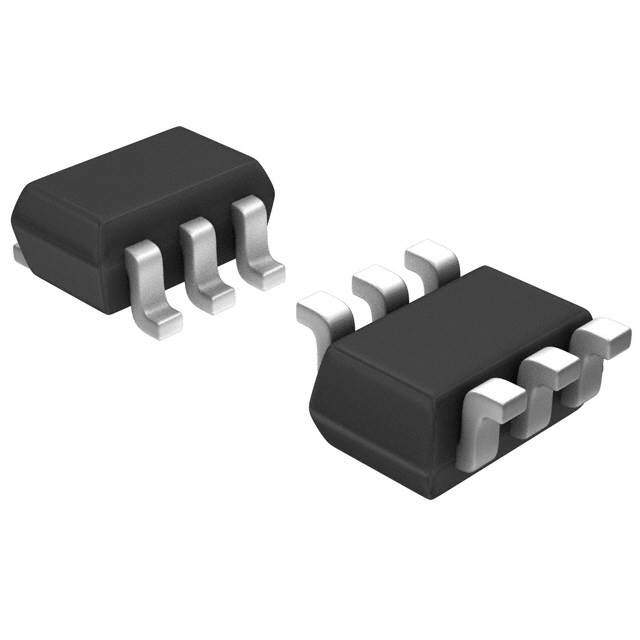
ICGOO电子元器件商城为您提供TPS61222MDCKTEP由Texas Instruments设计生产,在icgoo商城现货销售,并且可以通过原厂、代理商等渠道进行代购。 TPS61222MDCKTEP价格参考。Texas InstrumentsTPS61222MDCKTEP封装/规格:PMIC - 稳压器 - DC DC 开关稳压器, 固定 升压 开关稳压器 IC 正 5V 1 输出 200mA(开关) 6-TSSOP,SC-88,SOT-363。您可以下载TPS61222MDCKTEP参考资料、Datasheet数据手册功能说明书,资料中有TPS61222MDCKTEP 详细功能的应用电路图电压和使用方法及教程。
TPS61222MDCKTEP 是 Texas Instruments(德州仪器)生产的一款高效、同步整流的 DC-DC 升压(Boost)转换器,属于 PMIC(电源管理集成电路)中的开关稳压器类别。该器件广泛应用于需要高效升压和小尺寸设计的便携式电子产品中。

其典型应用场景包括:

1. 便携式电子设备:如智能手机、平板电脑、电子书阅读器等,用于将电池电压升压至适合系统使用的电压,例如驱动显示屏或为其他子系统供电。

2. 无线传感器网络:用于低功耗无线节点,将电池电压升压以供无线收发器或微控制器使用。

3. 穿戴设备:如智能手表、健康监测设备等,适用于对空间和功耗要求严格的场景。

4. 工业控制系统:用于为传感器、执行器或小型电机提供稳定电源。

5. LED 驱动:可用于驱动低功率 LED 灯串,提供恒定亮度。

该芯片具有高效率(可达 95%)、小封装(SOT23-5)、宽输入电压范围(1.8V 至 5.5V)和可调输出电压(最高可达 5.5V)等特点,非常适合电池供电系统中使用。
| 参数 | 数值 |
| 产品目录 | 集成电路 (IC)半导体 |
| 描述 | IC REG BOOST SYNC 5V SC70-6稳压器—开关式稳压器 Boost Converter with 5.5 A Quiescnt Crrnt |
| 产品分类 | |
| 品牌 | Texas Instruments |
| 产品手册 | |
| 产品图片 |
|
| rohs | 符合RoHS无铅 / 符合限制有害物质指令(RoHS)规范要求 |
| 产品系列 | 电源管理 IC,稳压器—开关式稳压器,Texas Instruments TPS61222MDCKTEP- |
| 数据手册 | |
| 产品型号 | TPS61222MDCKTEP |
| PWM类型 | 电流模式 |
| 产品种类 | 稳压器—开关式稳压器 |
| 供应商器件封装 | SC-70-6 |
| 其它名称 | 296-34978-6 |
| 包装 | Digi-Reel® |
| 同步整流器 | 是 |
| 商标 | Texas Instruments |
| 安装类型 | 表面贴装 |
| 安装风格 | SMD/SMT |
| 封装 | Reel |
| 封装/外壳 | 6-TSSOP,SC-88,SOT-363 |
| 封装/箱体 | SC-70-6 |
| 工作温度 | -55°C ~ 125°C |
| 工作温度范围 | - 55 C to + 125 C |
| 工厂包装数量 | 250 |
| 开关频率 | 2 MHz |
| 拓扑结构 | Boost |
| 最大工作温度 | + 125 C |
| 最大输入电压 | 5.5 V |
| 最小工作温度 | - 55 C |
| 最小输入电压 | 0.7 V |
| 标准包装 | 1 |
| 电压-输入 | 0.7 V ~ 5.5 V |
| 电压-输出 | 5V |
| 电流-输出 | 200mA |
| 类型 | Voltage Converter |
| 系列 | TPS61222-EP |
| 输入电压 | 0.7 V to 5.5 V |
| 输出数 | 1 |
| 输出电压 | 5 V |
| 输出电流 | 400 mA |
| 输出端数量 | 1 Output |
| 输出类型 | 固定 |
| 频率-开关 | 最高 2MHz |


- 商务部:美国ITC正式对集成电路等产品启动337调查
- 曝三星4nm工艺存在良率问题 高通将骁龙8 Gen1或转产台积电
- 太阳诱电将投资9.5亿元在常州建新厂生产MLCC 预计2023年完工
- 英特尔发布欧洲新工厂建设计划 深化IDM 2.0 战略
- 台积电先进制程称霸业界 有大客户加持明年业绩稳了
- 达到5530亿美元!SIA预计今年全球半导体销售额将创下新高
- 英特尔拟将自动驾驶子公司Mobileye上市 估值或超500亿美元
- 三星加码芯片和SET,合并消费电子和移动部门,撤换高东真等 CEO
- 三星电子宣布重大人事变动 还合并消费电子和移动部门
- 海关总署:前11个月进口集成电路产品价值2.52万亿元 增长14.8%


PDF Datasheet 数据手册内容提取
TPS61222-EP www.ti.com SLVSBI2–SEPTEMBER2012 LOW INPUT VOLTAGE, 0.7-V BOOST CONVERTER WITH 5.5-μA QUIESCENT CURRENT CheckforSamples:TPS61222-EP FEATURES 1 • Upto95%EfficiencyatTypicalOperating APPLICATIONS Conditions • BatteryPoweredApplications • 5.5μAQuiescentCurrent – 1to3CellAlkaline,NiCdorNiMH • StartupIntoLoadat0.7VInputVoltage – 1CellLi-IonorLi-Primary • OperatingInputVoltagefrom0.7Vto5.5V • SolarorFuelCellPoweredApplications • Pass-ThroughFunctionDuringShutdown • ConsumerandPortableMedicalProducts • MinimumSwitchingCurrent200mA • PersonalCareProducts • Protections: • WhiteorStatusLEDs – OutputOvervoltage • Smartphones – Overtemperature – InputUndervoltageLockout SUPPORTS DEFENSE, AEROSPACE, AND MEDICAL APPLICATIONS • FixedOutputVoltageVersions • Small6-PinSC-70Package • ControlledBaseline • OneAssemblyandTestSite • OneFabricationSite • AvailableinMilitary(–55°Cto125°C) TemperatureRange (1) • ExtendedProductLifeCycle • ExtendedProduct-ChangeNotification • ProductTraceability (1) Customtemperaturerangesavailable DESCRIPTION The TPS61222 provides a power-supply solution for products powered by either a single-cell, two-cell, or three- cell alkaline, NiCd or NiMH, or one-cell Li-Ion or Li-polymer battery. Possible output currents depend on the input-to-output voltage ratio. The boost converter is based on a hysteretic controller topology using synchronous rectification to obtain maximum efficiency at minimal quiescent currents. The output voltage of the adjustable version can be programmed by an external resistor divider, or is set internally to a fixed output voltage. The converter can be switched off by a featured enable pin. While being switched off, battery drain is minimized. The deviceisofferedina6-pinSC-70package(DCK)measuring2mmx2mmtoenablesmallcircuitlayoutsize. 1 Pleasebeawarethatanimportantnoticeconcerningavailability,standardwarranty,anduseincriticalapplicationsof TexasInstrumentssemiconductorproductsanddisclaimerstheretoappearsattheendofthisdatasheet. PRODUCTIONDATAinformationiscurrentasofpublicationdate. Copyright©2012,TexasInstrumentsIncorporated Products conform to specifications per the terms of the Texas Instruments standard warranty. Production processing does not necessarilyincludetestingofallparameters.
TPS61222-EP SLVSBI2–SEPTEMBER2012 www.ti.com This integrated circuit can be damaged by ESD. Texas Instruments recommends that all integrated circuits be handled with appropriateprecautions.Failuretoobserveproperhandlingandinstallationprocedurescancausedamage. ESDdamagecanrangefromsubtleperformancedegradationtocompletedevicefailure.Precisionintegratedcircuitsmaybemore susceptibletodamagebecauseverysmallparametricchangescouldcausethedevicenottomeetitspublishedspecifications. AVAILABLEDEVICEOPTIONS(1) PACKAGE T PACKAGE(2) PARTNUMBER VIDNUMBER J MARKING –55°Cto125°C SHL 6-PinSC-70 TPS61222MDCKTEP V62/12603-01XE (1) Contactthefactorytocheckavailabilityofotherfixedoutputvoltageversions. (2) Forthemostcurrentpackageandorderinginformation,seethePackageOptionAddendumattheendofthisdocument,orseetheTI websiteatwww.ti.com. ABSOLUTE MAXIMUM RATINGS overoperatingfree-airtemperaturerange(unlessotherwisenoted)(1) UNIT V InputvoltagerangeonVIN,L,VOUT,EN,FB –0.3to7.5 V IN T Operatingjunctiontemperaturerange –55to145 °C J T Storagetemperaturerange –65to150 °C stg HumanBodyModel(HBM)(2) 2 kV ESD MachineModel(MM)(2) 200 V ChargedDeviceModel(CDM)(2) 1.5 kV (1) StressesbeyondthoselistedunderAbsoluteMaximumRatingsmaycausepermanentdamagetothedevice.Thesearestressratings only,andfunctionaloperationofthedeviceattheseoranyotherconditionsbeyondthoseindicatedunderRecommendedOperating Conditionsisnotimplied.Exposuretoabsolute-maximum-ratedconditionsforextendedperiodsmayaffectdevicereliability. (2) ESDtestingisperformedaccordingtotherespectiveJESD22JEDECstandard. THERMAL INFORMATION TPS61222 THERMALMETRIC(1) DCK UNITS 6PINS θ Junction-to-ambientthermalresistance(2) 231.2 JA θ Junction-to-case(top)thermalresistance(3) 61.8 JCtop θ Junction-to-boardthermalresistance(4) 78.8 JB °C/W ψ Junction-to-topcharacterizationparameter(5) 2.2 JT ψ Junction-to-boardcharacterizationparameter(6) 78 JB θ Junction-to-case(bottom)thermalresistance(7) N/A JCbot (1) Formoreinformationabouttraditionalandnewthermalmetrics,seetheICPackageThermalMetricsapplicationreport,SPRA953. (2) Thejunction-to-ambientthermalresistanceundernaturalconvectionisobtainedinasimulationonaJEDEC-standard,high-Kboard,as specifiedinJESD51-7,inanenvironmentdescribedinJESD51-2a. (3) Thejunction-to-case(top)thermalresistanceisobtainedbysimulatingacoldplatetestonthepackagetop.NospecificJEDEC- standardtestexists,butaclosedescriptioncanbefoundintheANSISEMIstandardG30-88. (4) Thejunction-to-boardthermalresistanceisobtainedbysimulatinginanenvironmentwitharingcoldplatefixturetocontrolthePCB temperature,asdescribedinJESD51-8. (5) Thejunction-to-topcharacterizationparameter,ψ ,estimatesthejunctiontemperatureofadeviceinarealsystemandisextracted JT fromthesimulationdataforobtainingθ ,usingaproceduredescribedinJESD51-2a(sections6and7). JA (6) Thejunction-to-boardcharacterizationparameter,ψ ,estimatesthejunctiontemperatureofadeviceinarealsystemandisextracted JB fromthesimulationdataforobtainingθ ,usingaproceduredescribedinJESD51-2a(sections6and7). JA (7) Thejunction-to-case(bottom)thermalresistanceisobtainedbysimulatingacoldplatetestontheexposed(power)pad.Nospecific JEDECstandardtestexists,butaclosedescriptioncanbefoundintheANSISEMIstandardG30-88. Spacer 2 SubmitDocumentationFeedback Copyright©2012,TexasInstrumentsIncorporated ProductFolderLinks:TPS61222-EP
TPS61222-EP www.ti.com SLVSBI2–SEPTEMBER2012 RECOMMENDED OPERATING CONDITIONS MIN NOM MAX UNIT V SupplyvoltageatVIN 0.7 5.5 V IN T Operatingfreeairtemperaturerange –55 125 °C J ELECTRICAL CHARACTERISTICS T =−55°Cto125°C,T =T andoverrecommendedinputvoltagerange(typicalatanambienttemperaturerangeof25°C) J J A (unlessotherwisenoted) DC/DCSTAGE PARAMETER TESTCONDITIONS MIN TYP MAX UNIT V Inputvoltagerange 0.7 5.5 V IN V Minimuminputvoltageatstartup R ≥150Ω 0.7 V IN Load V Outputvoltage(5V) V <V 4.8 5 5.19 V OUT IN OUT I Inductorcurrentripple 200 mA LH I Switchcurrentlimit V =5V,V =1.2V 200 400 mA SW OUT IN R Rectifyingswitchonresistance V =5V 700 mΩ DSon_HSD OUT R Mainswitchonresistance V =5V 550 mΩ DSon_LSD OUT Lineregulation V <V 0.5 % IN OUT Loadregulation V <V 0.5 % IN OUT Quiescent VIN 0.5 1.4 μA I I =0mA,V =V =1.2V,V =5V Q current V O EN IN OUT 5 8.5 μA OUT Shutdown I V V =0V,V =1.2V,V ≥V 0.2 0.96 μA SD current IN EN IN OUT IN I LeakagecurrentintoL V =0V,V =1.2V,V =1.2V,V ≥V 0.01 0.3 μA LKG_L EN IN L OUT IN I ENinputcurrent ClampedonGNDorV (V <1.5V) 0.005 0.13 μA EN IN IN CONTROLSTAGE PARAMETER TESTCONDITIONS MIN TYP MAX UNIT V ENinputlowvoltage V ≤1.5V 0.15×V V IL IN IN V ENinputhighvoltage V ≤1.5V 0.8×V V IH IN IN V ENinputlowvoltage 5V>V >1.5V 0.34 V IL IN V ENinputhighvoltage 5V>V >1.5V 1.28 V IH IN V Undervoltagelockoutthresholdforturnoff V decreasing 0.5 0.72 V UVLO IN Overvoltageprotectionthreshold 5.5 7.5 V Overtemperatureprotection 140 °C Overtemperaturehysteresis 20 °C Copyright©2012,TexasInstrumentsIncorporated SubmitDocumentationFeedback 3 ProductFolderLinks:TPS61222-EP
TPS61222-EP SLVSBI2–SEPTEMBER2012 www.ti.com 10000.00 Wirebond Voiding Fail Mode 1000.00 s) r a e Y e ( 100.00 Lif d e t ma Electromigration Failure Mode ti s E 10.00 1.00 80 90 100 110 120 130 140 150 160 Continuous T (°C) J (1) Seedatasheetforabsolutemaximumandminimumrecommendedoperatingconditions. (2) Silicon operating life design goal is 10 years at 105°C junction temperature (does not include package interconnect life). (3) Enhancedplasticproductdisclaimerapplies. Figure1. TPS61222-EPOperatingLifeDeratingChart 4 SubmitDocumentationFeedback Copyright©2012,TexasInstrumentsIncorporated ProductFolderLinks:TPS61222-EP
TPS61222-EP www.ti.com SLVSBI2–SEPTEMBER2012 PIN ASSIGNMENTS DCK PACKAGE (TOPVIEW) VIN EN FB L GND VOUT TerminalFunctions TERMINAL I/O DESCRIPTION NAME NO. EN 6 I Enableinput(1:enabled,0:disabled).Mustbeactivelytiedhighorlow. FB 2 I Voltagefeedbackofadjustableversion.MustbeconnectedtoV atfixedoutputvoltageversions. OUT GND 3 Control/logicandpowerground L 5 I ConnectionforInductor VIN 1 I Boostconverterinputvoltage VOUT 4 O Boostconverteroutputvoltage FUNCTIONALBLOCKDIAGRAM L VOUT VOUT VIN Gate Driver VIN Start Up Current Sensor FB DDeevviiccee EN CCoonnttrrooll GND VREF Copyright©2012,TexasInstrumentsIncorporated SubmitDocumentationFeedback 5 ProductFolderLinks:TPS61222-EP
TPS61222-EP SLVSBI2–SEPTEMBER2012 www.ti.com PARAMETER MEASUREMENT INFORMATION L 1 L VOUT V OUT R 1 V VIN FB C IN R 2 EN 2 C 1 GND TPS6122x Table1.ListofComponents(1) COMPONENT PARTNUMBER MANUFACTURER VALUE REFERENCE C GRM188R60J106ME84D Murata 10μF,6.3V.X5RCeramic 1 C GRM188R60J106ME84D Murata 10μF,6.3V.X5RCeramic 2 L EPL3015-472MLB Coilcraft 4.7μH 1 adjustableversion:Valuesdependingonthe R ,R programmedoutputvoltage 1 2 fixedversion:R =0Ω,R notused 1 2 (1) Designwastestedusingthesecomponentsat25°Cambienttemperature. 6 SubmitDocumentationFeedback Copyright©2012,TexasInstrumentsIncorporated ProductFolderLinks:TPS61222-EP
TPS61222-EP www.ti.com SLVSBI2–SEPTEMBER2012 TYPICAL CHARACTERISTICS Table of Graphs FIGURE MaximumOutputCurrent vsInputVoltage Figure2 vsOutputCurrent,V =[0.7V;1.2V;2.4V;3.6V;4.2V] Figure3 IN Efficiency vsInputVoltage,I =[100uA;1mA;10mA;50mA] Figure4 OUT InputCurrent atNoOutputLoad,DeviceEnabled Figure5 OutputVoltage vsOutputCurrent,V =[0.7V;1.2V;2.4V;3.6V] Figure6 IN LoadTransientResponse,V =2.4V,I =14mAto126mA Figure7 IN OUT Waveforms LineTransientResponse,V =2.8Vto3.6V,R =100Ω Figure8 IN LOAD MAXIMUMOUTPUTCURRENT EFFICIENCY vs vs INPUTVOLTAGE OUTPUTCURRENTANDINPUTVOLTAGE 300 100 VO= 5 V VO= 5 V 90 250 A 80 m nt - 200 70 mum output Curre 115000 - Efficiency - %h 456000 VI= 0.7 V VI= 1.2 VVI= 2.4 V VI= 3.6 V VI= 4.2 V xi 30 a M 50 20 10 0 0 0.7 1.2 1.7 2.2 2.7 3.2 3.7 4.2 4.7 0.01 0.1 1 10 100 VI- Input Voltage - V IO- Output Current - mA Figure2. Figure3. EFFICIENCY NOLOADINPUTCURRENT vs vs INPUTVOLTAGEANDOUTPUTCURRENT INPUTVOLTAGE,DEVICEENABLED 100 80 VO= 5 V VO= 5 V Device Enabled 70 80 IO= 10 mA IO= 50 mA 60 - Efficiency - %h 4600 IO= 100mAIO= 1 mA nput Current -Am 345000 - I II 20 20 10 0 0 0.7 1.7 2.7 3.7 4.7 0.7 1.7 2.7 3.7 4.7 VI- Input Voltage - V VI- Input Voltage - V Figure4. Figure5. Copyright©2012,TexasInstrumentsIncorporated SubmitDocumentationFeedback 7 ProductFolderLinks:TPS61222-EP
TPS61222-EP SLVSBI2–SEPTEMBER2012 www.ti.com OUTPUTVOLTAGE vs OUTPUTCURRENTANDINPUTVOLTAGE LOADTRANSIENTRESPONSE 5.2 Offset: 0A VO= 5 V IL 200 mA/div 5.1 V ge - VI= 3.6 V IO a olt 50 mA/div Offset: 0A ut V 5 utp VI= 2.4 V - O VI= 1.2 V VO VO4.9 VI= 0.7 V 50 mV/div Offset: 5 V VI= 2.4 V, IO= 14 mAto 126 mA 4.8 0.01 0.1 1 10 100 200ms/div IO- Output Current - mA Figure6. Figure7. LINETRANSIENTRESPONSE VI 200 mV/div Offset: 2.8 V VO 20 mV/div VI2.8 to 3.6 V, RLOAD= 100W, trise= tfall= 20 ms Offset: 5 V 200ms/div Figure8. 8 SubmitDocumentationFeedback Copyright©2012,TexasInstrumentsIncorporated ProductFolderLinks:TPS61222-EP
TPS61222-EP www.ti.com SLVSBI2–SEPTEMBER2012 DETAILED DESCRIPTION OPERATION The TPS61222 is a high performance, high efficient switching boost converter. To achieve high efficiency the power stage is realized as a synchronous boost topology. For the power switching two actively controlled low R powerMOSFETsareimplemented. DSon CONTROLLER CIRCUIT The device is controlled by a hysteretic current mode controller. This controller regulates the output voltage by keeping the inductor ripple current constant in the range of 200 mA and adjusting the offset of this inductor current depending on the output load. In case the required average input current is lower than the average inductor current defined by this constant ripple the inductor current gets discontinuous to keep the efficiency high atlowloadconditions. I L Continuous Current Operation Discontinuous Current Operation 200 mA (typ.) 200 mA (typ.) t Figure9. HystereticCurrentOperation The output voltage V is monitored via the feedback network which is connected to the voltage error amplifier. OUT To regulate the output voltage, the voltage error amplifier compares this feedback voltage to the internal voltage reference and adjusts the required offset of the inductor current accordingly. At fixed output voltage versions an internal feedback network is used to program the output voltage, at adjustable versions an external resistor dividerneedstobeconnected. The self oscillating hysteretic current mode architecture is inherently stable and allows fast response to load variations.Italsoallowsusinginductorsandcapacitorsoverawidevaluerange. DeviceEnableandShutdownMode ThedeviceisenabledwhenENissethighandshutdownwhenENislow.Duringshutdown,theconverterstops switching and all internal control circuitry is turned off. In this case the input voltage is connected to the output throughtheback-gatediodeoftherectifyingMOSFET.Thismeansthattherealwayswillbevoltageattheoutput whichcanbeashighastheinputvoltageorlowerdependingontheload. Startup After the EN pin is tied high, the device starts to operate. In case the input voltage is not high enough to supply the control circuit properly a startup oscillator starts to operate the switches. During this phase the switching frequency is controlled by the oscillator and the maximum switch current is limited. As soon as the device has built up the output voltage to about 1.8V, high enough for supplying the control circuit, the device switches to its normalhystereticcurrentmodeoperation.Thestartuptimedependsoninputvoltageandloadcurrent. OperationatOutputOverload If in normal boost operation the inductor current reaches the internal switch current limit threshold the main switchisturnedofftostopfurtherincreaseoftheinputcurrent. In this case the output voltage will decrease since the device can not provide sufficient power to maintain the set outputvoltage. Iftheoutputvoltagedropsbelowtheinputvoltagethebackgatediodeoftherectifyingswitchgetsforwardbiased and current starts flow through it. This diode cannot be turned off, so the current finally is only limited by the remaining DC resistances. As soon as the overload condition is removed, the converter resumes providing the setoutputvoltage. Copyright©2012,TexasInstrumentsIncorporated SubmitDocumentationFeedback 9 ProductFolderLinks:TPS61222-EP
TPS61222-EP SLVSBI2–SEPTEMBER2012 www.ti.com UndervoltageLockout An implemented undervoltage lockout function stops the operation of the converter if the input voltage drops below the typical undervoltage lockout threshold. This function is implemented in order to prevent malfunctioning oftheconverter. OvervoltageProtection If, for any reason, the output voltage is not fed back properly to the input of the voltage amplifier, control of the output voltage will not work anymore. Therefore an overvoltage protection is implemented to avoid the output voltage exceeding critical values for the device and possibly for the system it is supplying. For this protection the TPS61222 output voltage is also monitored internally. In case it reaches the internally programmed threshold of 6.5Vtypicallythevoltageamplifierregulatestheoutputvoltagetothisvalue. IftheTPS61222isusedtodriveLEDs,thisfeatureprotectsthecircuitiftheLEDfails. OvertemperatureProtection The device has a built-in temperature sensor which monitors the internal IC junction temperature. If the temperature exceeds the programmed threshold (see electrical characteristics table), the device stops operating. As soon as the IC temperature has decreased below the programmed threshold, it starts operating again. To preventunstableoperationclosetotheregionofovertemperaturethreshold,abuilt-inhysteresisisimplemented. 10 SubmitDocumentationFeedback Copyright©2012,TexasInstrumentsIncorporated ProductFolderLinks:TPS61222-EP
TPS61222-EP www.ti.com SLVSBI2–SEPTEMBER2012 APPLICATION INFORMATION DESIGN PROCEDURE The TPS61222 DC/DC converter is intended for systems powered by a single cell battery to up to three Alkaline, NiCd or NiMH cells with a typical terminal voltage between 0.7 V and 5.5 V. It can also be used in systems powered by one-cell Li-Ion or Li-Polymer batteries with a typical voltage between 2.5 V and 4.2 V. Additionally, anyothervoltagesourcewithatypicaloutputvoltagebetween0.7Vand5.5VcanbeusedwiththeTPS61222. Programming the Output Voltage Outputvoltage The output voltage is set by a resistor divider internally. The FB pin is used to sense the output voltage. To configure the fixed output devices properly, the FB pin needs to be connected directly to VOUT as shown in Figure10. L 1 L VOUT V OUT V VIN FB C IN 2 EN C 1 GND TPS61222 Figure10. TypicalApplicationCircuit Inductor Selection TomakesurethattheTPS61222canoperate,asuitableinductormustbeconnectedbetweenpinVINandpinL. Inductorvaluesof4.7μHshowgoodperformanceoverthewholeinputandoutputvoltagerange. Choosingotherinductancevaluesaffectstheswitchingfrequencyfproportionalto1/LasshowninEquation1. 1 V ´(V -V ) L= ´ IN OUT IN f´200 mA V OUT (1) Choosing inductor values higher than 4.7 μH can improve efficiency due to reduced switching frequency and thereforewithreducedswitchinglosses.Usinginductorvaluesbelow2.2μHisnotrecommended. Having selected an inductance value, the peak current for the inductor in steady state operation can be calculated.Equation2givesthepeakcurrentestimate. ì V ´ I ï OUT OUT +100mA; continouscurrentoperation IL,MAX = í 0.8´VIN ï î200mA; discontinuouscurrentoperation (2) For selecting the inductor this would be the suitable value for the current rating. It also needs to be taken into accountthatloadtransientsanderrorconditionsmaycausehigherinductorcurrents. Equation 3 provides an easy way to estimate whether the device will work in continuous or discontinuous operation depending on the operating points. As long as the inequation is true, continuous operation is typically established.Iftheinequationbecomesfalse,discontinousoperationistypicallyestablished. V ´I OUT OUT >0.8´100 mA V IN (3) Copyright©2012,TexasInstrumentsIncorporated SubmitDocumentationFeedback 11 ProductFolderLinks:TPS61222-EP
TPS61222-EP SLVSBI2–SEPTEMBER2012 www.ti.com ThefollowinginductorseriesfromdifferentsuppliershavebeenusedwithTPS61222converters: Table2.ListofInductors(1) VENDOR INDUCTORSERIES EPL3015 Coilcraft EPL2010 Murata LQH3NP TajoYuden NR3015 WurthElektronik WE-TPCTypS (1) Designwastestedusingthesecomponentsat25°Cambient temperature. Capacitor Selection InputCapacitor At least a 10-μF input capacitor is recommended to improve transient behavior of the regulator and EMI behavior of the total power supply circuit. A ceramic capacitor placed as close as possible to the VIN and GND pins of the ICisrecommended. OutputCapacitor For the output capacitor C , it is recommended to use small ceramic capacitors placed as close as possible to 2 the VOUT and GND pins of the IC. If, for any reason, the application requires the use of large capacitors which can not be placed close to the IC, the use of a small ceramic capacitor with an capacitance value of around 2.2μF in parallel to the large one is recommended. This small capacitor should be placed as close as possible to theVOUTandGNDpinsoftheIC. A minimum capacitance value of 4.7 μF should be used, 10 μF are recommended. If the inductor value exceeds 4.7 μH, the value of the output capacitance value needs to be half the inductance value or higher for stability reasons,seeEquation4. L C ³ ´ 2 2 (4) The TPS61222 is not sensitive to the ESR in terms of stability. Using low ESR capacitors, such as ceramic capacitors, is recommended anyway to minimize output voltage ripple. If heavy load changes are expected, the outputcapacitorvalueshouldbeincreasedtoavoidoutputvoltagedropsduringfastloadtransients. Layout Considerations As for all switching power supplies, the layout is an important step in the design, especially at high peak currents and high switching frequencies. If the layout is not carefully done, the regulator could show stability problems as well as EMI problems. Therefore, use wide and short traces for the main current path and for the power ground paths.Theinputandoutputcapacitor,aswellastheinductorshouldbeplacedascloseaspossibletotheIC. The feedback divider should be placed as close as possible to the control ground pin of the IC. To lay out the ground, it is recommended to use short traces as well, separated from the power ground traces. This avoids ground shift problems, which can occur due to superimposition of power ground current and control ground current.AssurethatthegroundtracesareconnectedclosetothedeviceGNDpin. THERMAL INFORMATION Implementation of integrated circuits in low-profile and fine-pitch surface-mount packages typically requires special attention to power dissipation. Many system-dependent issues such as thermal coupling, airflow, added heat sinks and convection surfaces, and the presence of other heat-generating components affect the power- dissipationlimitsofagivencomponent. 12 SubmitDocumentationFeedback Copyright©2012,TexasInstrumentsIncorporated ProductFolderLinks:TPS61222-EP
TPS61222-EP www.ti.com SLVSBI2–SEPTEMBER2012 Threebasicapproachesforenhancingthermalperformancearelistedbelow. • Improvingthepower-dissipationcapabilityofthePCBdesign • ImprovingthethermalcouplingofthecomponenttothePCB • Introducingairflowinthesystem For more details on how to use the thermal parameters in the dissipation ratings table please check the Thermal CharacteristicsApplicationNote(SZZA017)andtheICPackageThermalMetricsApplicationNote(SPRA953). Copyright©2012,TexasInstrumentsIncorporated SubmitDocumentationFeedback 13 ProductFolderLinks:TPS61222-EP
PACKAGE OPTION ADDENDUM www.ti.com 6-Feb-2020 PACKAGING INFORMATION Orderable Device Status Package Type Package Pins Package Eco Plan Lead/Ball Finish MSL Peak Temp Op Temp (°C) Device Marking Samples (1) Drawing Qty (2) (6) (3) (4/5) TPS61222MDCKTEP ACTIVE SC70 DCK 6 250 Green (RoHS NIPDAU Level-1-260C-UNLIM -55 to 125 SHL & no Sb/Br) V62/12603-01XE ACTIVE SC70 DCK 6 250 Green (RoHS NIPDAU Level-1-260C-UNLIM -55 to 125 SHL & no Sb/Br) (1) The marketing status values are defined as follows: ACTIVE: Product device recommended for new designs. LIFEBUY: TI has announced that the device will be discontinued, and a lifetime-buy period is in effect. NRND: Not recommended for new designs. Device is in production to support existing customers, but TI does not recommend using this part in a new design. PREVIEW: Device has been announced but is not in production. Samples may or may not be available. OBSOLETE: TI has discontinued the production of the device. (2) RoHS: TI defines "RoHS" to mean semiconductor products that are compliant with the current EU RoHS requirements for all 10 RoHS substances, including the requirement that RoHS substance do not exceed 0.1% by weight in homogeneous materials. Where designed to be soldered at high temperatures, "RoHS" products are suitable for use in specified lead-free processes. TI may reference these types of products as "Pb-Free". RoHS Exempt: TI defines "RoHS Exempt" to mean products that contain lead but are compliant with EU RoHS pursuant to a specific EU RoHS exemption. Green: TI defines "Green" to mean the content of Chlorine (Cl) and Bromine (Br) based flame retardants meet JS709B low halogen requirements of <=1000ppm threshold. Antimony trioxide based flame retardants must also meet the <=1000ppm threshold requirement. (3) MSL, Peak Temp. - The Moisture Sensitivity Level rating according to the JEDEC industry standard classifications, and peak solder temperature. (4) There may be additional marking, which relates to the logo, the lot trace code information, or the environmental category on the device. (5) Multiple Device Markings will be inside parentheses. Only one Device Marking contained in parentheses and separated by a "~" will appear on a device. If a line is indented then it is a continuation of the previous line and the two combined represent the entire Device Marking for that device. (6) Lead/Ball Finish - Orderable Devices may have multiple material finish options. Finish options are separated by a vertical ruled line. Lead/Ball Finish values may wrap to two lines if the finish value exceeds the maximum column width. Important Information and Disclaimer:The information provided on this page represents TI's knowledge and belief as of the date that it is provided. TI bases its knowledge and belief on information provided by third parties, and makes no representation or warranty as to the accuracy of such information. Efforts are underway to better integrate information from third parties. TI has taken and continues to take reasonable steps to provide representative and accurate information but may not have conducted destructive testing or chemical analysis on incoming materials and chemicals. TI and TI suppliers consider certain information to be proprietary, and thus CAS numbers and other limited information may not be available for release. In no event shall TI's liability arising out of such information exceed the total purchase price of the TI part(s) at issue in this document sold by TI to Customer on an annual basis. Addendum-Page 1
PACKAGE OPTION ADDENDUM www.ti.com 6-Feb-2020 OTHER QUALIFIED VERSIONS OF TPS61222-EP : •Catalog: TPS61222 NOTE: Qualified Version Definitions: •Catalog - TI's standard catalog product Addendum-Page 2
PACKAGE MATERIALS INFORMATION www.ti.com 15-Feb-2014 TAPE AND REEL INFORMATION *Alldimensionsarenominal Device Package Package Pins SPQ Reel Reel A0 B0 K0 P1 W Pin1 Type Drawing Diameter Width (mm) (mm) (mm) (mm) (mm) Quadrant (mm) W1(mm) TPS61222MDCKTEP SC70 DCK 6 250 178.0 8.4 2.4 2.5 1.2 4.0 8.0 Q3 PackMaterials-Page1
PACKAGE MATERIALS INFORMATION www.ti.com 15-Feb-2014 *Alldimensionsarenominal Device PackageType PackageDrawing Pins SPQ Length(mm) Width(mm) Height(mm) TPS61222MDCKTEP SC70 DCK 6 250 180.0 180.0 18.0 PackMaterials-Page2
None
None
IMPORTANTNOTICEANDDISCLAIMER TI PROVIDES TECHNICAL AND RELIABILITY DATA (INCLUDING DATASHEETS), DESIGN RESOURCES (INCLUDING REFERENCE DESIGNS), APPLICATION OR OTHER DESIGN ADVICE, WEB TOOLS, SAFETY INFORMATION, AND OTHER RESOURCES “AS IS” AND WITH ALL FAULTS, AND DISCLAIMS ALL WARRANTIES, EXPRESS AND IMPLIED, INCLUDING WITHOUT LIMITATION ANY IMPLIED WARRANTIES OF MERCHANTABILITY, FITNESS FOR A PARTICULAR PURPOSE OR NON-INFRINGEMENT OF THIRD PARTY INTELLECTUAL PROPERTY RIGHTS. These resources are intended for skilled developers designing with TI products. You are solely responsible for (1) selecting the appropriate TI products for your application, (2) designing, validating and testing your application, and (3) ensuring your application meets applicable standards, and any other safety, security, or other requirements. These resources are subject to change without notice. TI grants you permission to use these resources only for development of an application that uses the TI products described in the resource. Other reproduction and display of these resources is prohibited. No license is granted to any other TI intellectual property right or to any third party intellectual property right. TI disclaims responsibility for, and you will fully indemnify TI and its representatives against, any claims, damages, costs, losses, and liabilities arising out of your use of these resources. TI’s products are provided subject to TI’s Terms of Sale (www.ti.com/legal/termsofsale.html) or other applicable terms available either on ti.com or provided in conjunction with such TI products. TI’s provision of these resources does not expand or otherwise alter TI’s applicable warranties or warranty disclaimers for TI products. Mailing Address: Texas Instruments, Post Office Box 655303, Dallas, Texas 75265 Copyright © 2020, Texas Instruments Incorporated