ICGOO在线商城 > 集成电路(IC) > PMIC - 稳压器 - DC DC 开关稳压器 > TPS61170DRVT
 Datasheet下载
- 型号: TPS61170DRVT
- 制造商: Texas Instruments
- 库位|库存: xxxx|xxxx
- 要求:
| 数量阶梯 | 香港交货 | 国内含税 |
| +xxxx | $xxxx | ¥xxxx |
查看当月历史价格
查看今年历史价格
TPS61170DRVT产品简介:
ICGOO电子元器件商城为您提供TPS61170DRVT由Texas Instruments设计生产,在icgoo商城现货销售,并且可以通过原厂、代理商等渠道进行代购。 TPS61170DRVT价格参考。Texas InstrumentsTPS61170DRVT封装/规格:PMIC - 稳压器 - DC DC 开关稳压器, Boost, Buck-Boost, Flyback, SEPIC Switching Regulator IC Positive Adjustable 3V 1 Output 960mA (Switch) 6-WDFN Exposed Pad。您可以下载TPS61170DRVT参考资料、Datasheet数据手册功能说明书,资料中有TPS61170DRVT 详细功能的应用电路图电压和使用方法及教程。
TPS61170DRVT是Texas Instruments(德州仪器)推出的一款高效、升压型DC-DC开关稳压器,属于PMIC中的开关稳压器类别。该器件采用6引脚SOT-23封装,具有低静态电流和高效率的特点,输入电压范围为0.9V至5.5V,可提供最高达5.5V的输出电压,最大输出电流可达1.4A(取决于输入电压),适用于多种便携式和低功耗应用场景。

典型应用场景包括:
1. 便携式电子设备:如智能手环、蓝牙耳机、手持医疗设备等,因其宽输入电压范围支持单节碱性电池或锂电池供电,适合电池供电系统。
2. 工业传感器与测量设备:在需要稳定升压电源的小型传感器模块中,TPS61170DRVT可将低电压电池升压至MCU或传感器所需的工作电压。
3. 物联网(IoT)终端设备:用于无线模块(如Wi-Fi、ZigBee、LoRa)的供电管理,确保在电池电压下降时仍能稳定工作。
4. 消费类电子产品:如电子玩具、遥控器、LED照明驱动等,利用其高集成度和小封装节省PCB空间。

该芯片具备软启动功能、过温保护和短路保护,提高了系统可靠性。其高达90%以上的转换效率有助于延长电池寿命,非常适合对功耗和尺寸敏感的应用。总之,TPS61170DRVT广泛应用于需要高效升压、小型化设计和长续航能力的低功耗系统中。
| 参数 | 数值 |
| 产品目录 | 集成电路 (IC)半导体 |
| 描述 | IC REG MULTI CONFIG ADJ 6SON稳压器—开关式稳压器 1.2A Sw Hi Vltg Boost Conv |
| 产品分类 | |
| 品牌 | Texas Instruments |
| 产品手册 | |
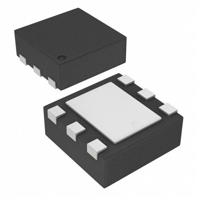
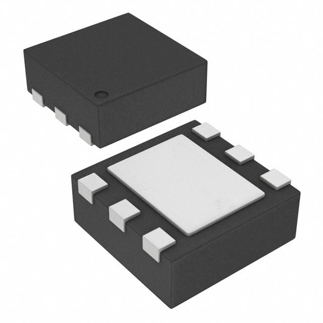
| 产品图片 |
|
| rohs | 符合RoHS无铅 / 符合限制有害物质指令(RoHS)规范要求 |
| 产品系列 | 电源管理 IC,稳压器—开关式稳压器,Texas Instruments TPS61170DRVT- |
| 数据手册 | |
| 产品型号 | TPS61170DRVT |
| PCN组件/产地 | |
| PWM类型 | 电流模式 |
| 产品种类 | 稳压器—开关式稳压器 |
| 供应商器件封装 | 6-SON(2x2) |
| 其它名称 | 296-32502-2 |
| 包装 | 带卷 (TR) |
| 同步整流器 | 无 |
| 商标 | Texas Instruments |
| 安装类型 | 表面贴装 |
| 安装风格 | SMD/SMT |
| 封装 | Reel |
| 封装/外壳 | 6-WDFN 裸露焊盘 |
| 封装/箱体 | WSON-6 |
| 工作温度 | -40°C ~ 85°C |
| 工作温度范围 | - 40 C to + 85 C |
| 工厂包装数量 | 250 |
| 开关频率 | 1.2 MHz |
| 拓扑结构 | Boost |
| 最大工作温度 | + 85 C |
| 最大输入电压 | 18 V |
| 最小工作温度 | - 40 C |
| 最小输入电压 | 3 V |
| 标准包装 | 250 |
| 电压-输入 | 3 V ~ 18 V |
| 电压-输出 | 3 V ~ 38 V |
| 电流-输出 | 1.2A |
| 类型 | 降压(降压),升压(升压),回扫,Sepic |
| 系列 | TPS61170 |
| 设计资源 | http://www.digikey.com/product-highlights/cn/zh/texas-instruments-webench-design-center/3176 |
| 输入电压 | 3 V to 18 V |
| 输出数 | 1 |
| 输出电压 | 3 V to 38 V |
| 输出电流 | 1.2 A |
| 输出端数量 | 1 Output |
| 输出类型 | 可调式 |
| 配用 | /product-detail/zh/TPS61170EVM-280/296-31229-ND/1907998/product-detail/zh/TPS61170EVM-316/296-31230-ND/2048000 |
| 频率-开关 | 1.2MHz |


- 商务部:美国ITC正式对集成电路等产品启动337调查
- 曝三星4nm工艺存在良率问题 高通将骁龙8 Gen1或转产台积电
- 太阳诱电将投资9.5亿元在常州建新厂生产MLCC 预计2023年完工
- 英特尔发布欧洲新工厂建设计划 深化IDM 2.0 战略
- 台积电先进制程称霸业界 有大客户加持明年业绩稳了
- 达到5530亿美元!SIA预计今年全球半导体销售额将创下新高
- 英特尔拟将自动驾驶子公司Mobileye上市 估值或超500亿美元
- 三星加码芯片和SET,合并消费电子和移动部门,撤换高东真等 CEO
- 三星电子宣布重大人事变动 还合并消费电子和移动部门
- 海关总署:前11个月进口集成电路产品价值2.52万亿元 增长14.8%


PDF Datasheet 数据手册内容提取
Product Sample & Technical Tools & Support & Folder Buy Documents Software Community TPS61170 SLVS789D–NOVEMBER2007–REVISEDDECEMBER2014 2 TPS61170 1.2-A High-Voltage Boost Converter in 2-mm x 2-mm QFN Package 1 Features 3 Description • 3-Vto18-VInputVoltageRange The TPS61170 is a monolithic, high-voltage switching 1 regulator with integrated 1.2-A, 40-V power MOSFET. • HighOutputVoltage:Upto38V The device can be configured in several standard • 1.2-AIntegratedSwitch switching-regulator topologies, including boost and • 1.2-MHzFixedSwitchingFrequency SEPIC. The device has a wide input-voltage range to support applications with input voltage from multicell • 12Vat300mAand24Vat150mAFrom5-V batteriesorregulated5-V,12-Vpowerrails. Input(Typical) The TPS61170 operates at a 1.2-MHz switching • Upto93%Efficiency frequency, allowing the use of low-profile inductors • On-The-FlyOutputVoltageReprogramming and low-value ceramic input and output capacitors. • Skip-SwitchingCycleforOutputRegulationat External loop compensation components give the LightLoad user flexibility to optimize loop compensation and • Built-inSoftStart transient response. The device has built-in protection features, such as pulse-by-pulse overcurrent limit, • 6-Pin,2-mm× 2-mmQFNPackage softstart,andthermalshutdown. 2 Applications The FB pin regulates to a reference voltage of 1.229 V. The reference voltage can be lowered using a 1- • 5-Vto12-Vand24-V,12-Vto24-VBoost wire digital interface (Easyscale™ protocol) through Converter the CTRL pin. Alternatively, a pulse width-modulation • BuckBoostRegulationUsingSEPICTopology (PWM) signal can be applied to the CTRL pin. The duty cycle of the signal reduces the feedback • ADSLModems referencevoltageproportionally. The TPS61170 is available in a 6-pin 2-mm × 2-mm QFN package, allowing a compact power-supply solution. DeviceInformation(1) PARTNUMBER PACKAGE BODYSIZE(NOM) TPS61170 VSON(6) 2.00mmx2.00mm (1) For all available packages, see the orderable addendum at theendofthedatasheet. 4 Typical Application Schematic L1 VIN 5 V 10mH D1 VOUT12 V/ 300 mA C1 C2 4.7mF 4.7mF TPS61170 R1 87.6 kW VIN SW CTRL FB R3 4.99 kW COMP GND R2 10 kW C3 10 nF L1:TOKO#A915_Y-100M C1: Murata GRM188R61A475K C2: Murata GRM21BR61E475K D1:ONsemi MBR0540T1 *R3, C3: Compensation RC network 1 An IMPORTANT NOTICE at the end of this data sheet addresses availability, warranty, changes, use in safety-critical applications, intellectualpropertymattersandotherimportantdisclaimers.PRODUCTIONDATA.
TPS61170 SLVS789D–NOVEMBER2007–REVISEDDECEMBER2014 www.ti.com Table of Contents 1 Features.................................................................. 1 8.5 Programming...........................................................12 2 Applications........................................................... 1 9 ApplicationandImplementation........................ 16 3 Description............................................................. 1 9.1 ApplicationInformation............................................16 4 TypicalApplicationSchematic............................. 1 9.2 TypicalApplication .................................................16 9.3 SystemExamples...................................................21 5 RevisionHistory..................................................... 2 10 PowerSupplyRecommendations..................... 23 6 PinConfigurationandFunctions......................... 3 11 Layout................................................................... 23 7 Specifications......................................................... 3 11.1 LayoutGuidelines.................................................23 7.1 AbsoluteMaximumRatings......................................3 11.2 LayoutExample....................................................24 7.2 ESDRatings..............................................................3 11.3 ThermalConsiderations........................................24 7.3 RecommendedOperatingConditions.......................4 12 DeviceandDocumentationSupport................. 25 7.4 ThermalInformation..................................................4 7.5 ElectricalCharacteristics...........................................5 12.1 DeviceSupport......................................................25 7.6 TypicalCharacteristics..............................................6 12.2 DocumentationSupport........................................25 12.3 Trademarks...........................................................25 8 DetailedDescription.............................................. 9 12.4 ElectrostaticDischargeCaution............................25 8.1 Overview...................................................................9 12.5 Glossary................................................................25 8.2 FunctionalBlockDiagram.........................................9 13 Mechanical,Packaging,andOrderable 8.3 FeatureDescription.................................................10 Information........................................................... 25 8.4 DeviceFunctionalModes........................................10 5 Revision History ChangesfromRevisionC(April2011)toRevisionD Page • AddedESDRatingstable,FeatureDescriptionsection,DeviceFunctionalModes,ApplicationandImplementation section,PowerSupplyRecommendationssection,Layoutsection,DeviceandDocumentationSupportsection,and Mechanical,Packaging,andOrderableInformationsection.................................................................................................. 1 ChangesfromRevisionB(November2009)toRevisionC Page • ChangedC1partnumberinFigure18,Figure19,andFigure20from"GRM188RA475K"to"GRM21BR61E475K"......21 2 SubmitDocumentationFeedback Copyright©2007–2014,TexasInstrumentsIncorporated ProductFolderLinks:TPS61170
TPS61170 www.ti.com SLVS789D–NOVEMBER2007–REVISEDDECEMBER2014 6 Pin Configuration and Functions QFNPackage 6Pins TopView FB VIN Thermal COMP CTRL Pad GND SW PinFunctions PIN I/O DESCRIPTION NAME NO. Outputofthetransconductanceerroramplifier.ConnectanexternalRCnetworktothispintocompensate COMP 2 O theregulator. Controlpinoftheboostregulator.CTRLisamultifunctionalpinwhichcanbeusedtoenablethedevice CTRL 5 I andcontrolthefeedbackvoltagewithaPWMsignalorfordigitalcommunications. FB 1 I Feedbackpinforcurrent.Connecttothecentertapofaresistordividertoprogramtheoutputvoltage. GND 3 O Ground SW 4 I ThisistheswitchingnodeoftheIC.ConnectSWtotheswitchedsideoftheinductor. Thethermalpadshouldbesolderedtotheanaloggroundplanetoavoidthermalissue.Ifpossible,use ThermalPad thermalviastoconnecttogroundplaneforidealpowerdissipation. VIN 6 I TheinputsupplypinfortheIC.ConnectVINtoasupplyvoltagefrom3Vto18V. 7 Specifications 7.1 Absolute Maximum Ratings overoperatingfree-airtemperaturerange(unlessotherwisenoted) (1) MIN MAX UNIT SupplyVoltagesonVIN (2) –0.3 20 V VoltagesonCTRL(2) –0.3 20 V V I VoltageonFBandCOMP(2) –0.3 3 V VoltageonSW(2) –0.3 40 V T OperatingJunctionTemperature –40 150 °C J T Storagetemperature –65 150 °C stg (1) Stressesbeyondthoselistedunderabsolutemaximumratingsmaycausepermanentdamagetothedevice.Thesearestressratings only,andfunctionaloperationofthedeviceattheseoranyotherconditionsbeyondthoseindicatedunderRecommendedOperating Conditionsisnotimplied.Exposuretoabsolute-maximum-ratedconditionsforextendedperiodsmayaffectdevicereliability. (2) Allvoltagevaluesarewithrespecttonetworkgroundterminal. 7.2 ESD Ratings VALUE UNIT Humanbodymodel(HBM),perANSI/ESDA/JEDECJS-001(1) ±2000 V(ESD) Electrostaticdischarge Charged-devicemodel(CDM),perJEDECspecificationJESD22- ±750 V C101(2) (1) JEDECdocumentJEP155statesthat500-VHBMallowssafemanufacturingwithastandardESDcontrolprocess.Manufacturingwith lessthan500-VHBMispossiblewiththenecessaryprecautions.Pinslistedas±2000Vmayactuallyhavehigherperformance. (2) JEDECdocumentJEP157statesthat250-VCDMallowssafemanufacturingwithastandardESDcontrolprocess.Manufacturingwith lessthan250-VCDMispossiblewiththenecessaryprecautions.Pinslistedas±750Vmayactuallyhavehigherperformance. Copyright©2007–2014,TexasInstrumentsIncorporated SubmitDocumentationFeedback 3 ProductFolderLinks:TPS61170
TPS61170 SLVS789D–NOVEMBER2007–REVISEDDECEMBER2014 www.ti.com 7.3 Recommended Operating Conditions MIN TYP MAX UNIT V Inputvoltagerange,VIN 3 18 V I V Outputvoltagerange VIN 38 V O L Inductor(1) 10 22 μH C Inputcapacitor 1 μF I C Outputcapacitor(1) 1 10 μF O T Operatingambienttemperature –40 85 °C A T Operatingjunctiontemperature –40 125 °C J (1) Thesevaluesarerecommendedvaluesthathavebeensuccessfullytestedinseveralapplications.Othervaluesmaybeacceptablein otherapplicationsbutshouldbefullytestedbytheuser. 7.4 Thermal Information TPS61170 THERMALMETRIC(1) DRV UNIT 6PINS R Junction-to-ambientthermalresistance 66.5 θJA R Junction-to-case(top)thermalresistance 85.6 θJC(top) R Junction-to-boardthermalresistance 36.0 θJB °C/W ψ Junction-to-topcharacterizationparameter 1.7 JT ψ Junction-to-boardcharacterizationparameter 36.4 JB R Junction-to-case(bottom)thermalresistance 7.1 θJC(bot) (1) Formoreinformationabouttraditionalandnewthermalmetrics,seetheICPackageThermalMetricsapplicationreport,SPRA953. 4 SubmitDocumentationFeedback Copyright©2007–2014,TexasInstrumentsIncorporated ProductFolderLinks:TPS61170
TPS61170 www.ti.com SLVS789D–NOVEMBER2007–REVISEDDECEMBER2014 7.5 Electrical Characteristics VIN=3.6V,CTRL=VIN,T =–40°Cto85°C,typicalvaluesareatT =25°C(unlessotherwisenoted) A A PARAMETER TESTCONDITIONS MIN TYP MAX UNIT SUPPLYCURRENT V Inputvoltagerange,VIN 3.0 18 V I I OperatingquiescentcurrentintoVIN DevicePWMswitchingnoload 2.3 mA Q I Shutdowncurrent CRTL=GND,VIN=4.2V 1 μA SD UVLO Under-voltagelockoutthreshold VINfalling 2.2 2.5 V V Under-voltagelockoutHysteresis 70 mV hys ENABLEANDREFERENCECONTROL V CTRLlogichighvoltage VIN=3Vto18V 1.2 V (CTRLh) V CTRLlogiclowvoltage VIN=3Vto18V 0.4 V (CTRL) R CTRLpulldownresistor 400 800 1600 kΩ (CTRL) t CTRLpulsewidthtoshutdown CTRLhightolow 2.5 ms off t EasyScaledetectiontime(1) CTRLpinlow 260 μs es_det t EasyScaledetectiondelay 100 μs es_delay t EasyScaledetectionwindowtime 1 ms es_win VOLTAGEANDCURRENTCONTROL V Voltagefeedbackregulationvoltage 1.204 1.229 1.254 V REF Voltagefeedbackregulationvoltageunder V V =492mV 477 492 507 mV (REF_PWM) reprogram FB I Voltagefeedbackinputbiascurrent V =1.229V 200 nA FB FB f Oscillatorfrequency 1.0 1.2 1.5 MHz S D Maximumdutycycle V =100mV 90% 93% max FB t Minimumonpulsewidth 40 ns min_on I Comppinsinkcurrent 100 μA sink I Comppinsourcecurrent 100 μA source G Erroramplifiertransconductance 240 320 400 μmho ea R Erroramplifieroutputresistance 5pFconnectedtoCOMP 6 MΩ ea f Erroramplifiercrossoverfrequency 5pFconnectedtoCOMP 500 kHz ea POWERSWITCH VIN=3.6V 0.3 0.6 R N-channelMOSFETon-resistance Ω DS(on) VIN=3.0V 0.7 I N-channelleakagecurrent V =35V,T =25°C 1 μA LN_NFET SW A OCandSS I N-ChannelMOSFETcurrentlimit D=D 0.96 1.2 1.44 A LIM max I Startupcurrentlimit D=D 0.7 A LIM_Start max t Timestepforhalfcurrentlimit 5 ms Half_LIM t Vreffiltertimeconstant 180 μs REF t V rampuptime 213 μs step REF (1) EasyScalecommunicationisallowedimmediatelyaftertheCTRLpinhasbeenlowformorethant .ToselectEasyScalemode,the es_det CTRLpinmustbelowformorethant theendoft . es_det es_win Copyright©2007–2014,TexasInstrumentsIncorporated SubmitDocumentationFeedback 5 ProductFolderLinks:TPS61170
TPS61170 SLVS789D–NOVEMBER2007–REVISEDDECEMBER2014 www.ti.com Electrical Characteristics (continued) VIN=3.6V,CTRL=VIN,T =–40°Cto85°C,typicalvaluesareatT =25°C(unlessotherwisenoted) A A PARAMETER TESTCONDITIONS MIN TYP MAX UNIT EasyScaleTIMING t Starttimeofprogramstream 2 μs start t Endtimeofprogramstream 2 360 μs EOS t Hightimelowbit Logic0 2 180 μs H_LB t Lowtimelowbit Logic0 2×t 360 μs L_LB H_LB t Hightimehighbit Logic1 2×t 360 μs H_HB L_HB t Lowtimehighbit Logic1 2 180 μs L_HB V Acknowledgeoutputvoltagelow Opendrain,R =15kΩtoVin 0.4 V ACKNL pullup t Acknowledgevalidtime See (2) 2 μs valACKN t Durationofacknowledgecondition See (2) 512 μs ACKN THERMALSHUTDOWN T Thermalshutdownthreshold 160 °C shutdown T Thermalshutdownthresholdhysteresis 15 °C hysteresis (2) Acknowledgeconditionactive0,thisconditionwillonlybeappliediftheRFAbitisset.Opendrainoutput,lineneedstobepulledhigh bythehostwithresistorload. 7.6 Typical Characteristics Table1.TableOfGraphs CircuitofFigure1,L=TOKOA915_Y-100M,D1=ONsemiMBR0540T1,unlessotherwisenoted. FIGURE Efficiency VIN=5V;VOUT=12V,18V,24V,30V Figure1 Efficiency VIN=5V,8.5V,12V;VOUT=24V Figure2 Outputvoltageaccuracy I =100mA Figure3 LOAD Switchcurrentlimit T =25°C Figure4 A Switchcurrentlimit Figure5 Erroramplifiertransconductance Figure6 EasyScalestep Figure7 PWMswitchingoperation VIN=5V;VOUT=12V;I =250mA Figure14 LOAD Loadtransientresponse VIN=5V;VOUT=12V;I =50mAto150mA Figure15 LOAD Start-up VIN=5V;VOUT=12V;I =250mA Figure16 LOAD Skip-cycleswitching VIN=9V;VOUT=12V,I =100μA Figure17 LOAD 6 SubmitDocumentationFeedback Copyright©2007–2014,TexasInstrumentsIncorporated ProductFolderLinks:TPS61170
TPS61170 www.ti.com SLVS789D–NOVEMBER2007–REVISEDDECEMBER2014 100 100 VIN = 5 V VOUT= 24 V VIN = 12 V VOUT= 12 V 90 90 VIN = 8.5 V VOUT= 30 V VOUT= 24 V VOUT= 18 V VIN = 5 V 80 80 % % Efficiency - 70 Efficiency - 70 60 60 50 50 40 40 0 50 100 150 200 250 300 0 50 100 150 200 250 300 Output Current - mA Output Current - mA Figure1.EfficiencyvsOutputCurrent Figure2.EfficiencyvsOutputCurrent 11.96 1600 I = 100 mA LOAD 1500 11.94 1400 V T = 25°C A ge - A mit - 1300 put Volta 11.92 TA= 85°C urrent Li 1200 Out TA= -40°C h C 1100 V- O11.90 Switc 1000 900 11.88 800 3 4 5 6 7 8 9 10 11 20 30 40 50 60 70 80 90 VI- Input Voltage - V Duty Cycle - % Figure3.OutputVoltagevsInputVoltage Figure4.SwitchCurrentLimitvsDutyCycle 1600 s 500 o h 1500 m A 1400 nce - 400 m a mit - 1300 duct 300 Li n urrent 1200 nsco Switch C 11010000 plifier Tra 120000 900 m A r 800-40 -20 0 20 40 60 80 100 120 140 Erro 0-40 -20 0 20 40 60 80 100 120 140 Temperature -°C Temperature -°C Figure5.SwitchCurrentLimitvsTemperature Figure6.ErrorAmplifierTransconductancevsTemperature Copyright©2007–2014,TexasInstrumentsIncorporated SubmitDocumentationFeedback 7 ProductFolderLinks:TPS61170
TPS61170 SLVS789D–NOVEMBER2007–REVISEDDECEMBER2014 www.ti.com 1.4 1.2 1 V ge - 0.8 a olt V B 0.6 F 0.4 0.2 0 0 2 4 6 8 10 12 14 16 18 20 22 24 26 28 30 32 Easy Scale Step Figure7.FBVoltagevsEasyScaleStep 8 SubmitDocumentationFeedback Copyright©2007–2014,TexasInstrumentsIncorporated ProductFolderLinks:TPS61170
TPS61170 www.ti.com SLVS789D–NOVEMBER2007–REVISEDDECEMBER2014 8 Detailed Description 8.1 Overview TheTPS61170integratesa40-VlowsideFETforprovidingoutputvoltagesupto38V.Thedeviceregulatesthe output with current mode PWM (pulse width modulation) control. The switching frequency of the PWM is fixed at 1.2 MHz (typical). The PWM control circuitry turns on the switch at the beginning of each switching cycle. The input voltage is applied across the inductor and stores the energy as the inductor current ramps up. During this portion of the switching cycle, the load current is provided by the output capacitor. When the inductor current rises to the threshold set by the error amplifier output, the power switch turns off and the external Schottky diode is forward biased. The inductor transfers stored energy to replenish the output capacitor and supply the load current. This operation repeats each switching cycle. As shown in the block diagram, the duty cycle of the converter is determined by the PWM control comparator which compares the error amplifier output and the currentsignal. A ramp signal from the oscillator is added to the current ramp. This slope compensation ramp is necessary to avoid subharmonic oscillations that are intrinsic to current mode control at duty cycles higher than 50%. The feedback loop regulates the FB pin to a reference voltage through an error amplifier. The output of the error amplifier must be connected to the COMP pin. An external RC compensation network must be connected to the COMPpintooptimizethefeedbackloopforstabilityandtransientresponse. 8.2 Functional Block Diagram C2 R1 D1 R2 1 4 L1 FB SW Band Gap Error Amplifer Vin 6 COMP 2 C1 PWM Control R3 Soft 5 CTRL Start-up C3 Ramp Generator + CSuernrseonrt Oscillator GND 3 Copyright©2007–2014,TexasInstrumentsIncorporated SubmitDocumentationFeedback 9 ProductFolderLinks:TPS61170
TPS61170 SLVS789D–NOVEMBER2007–REVISEDDECEMBER2014 www.ti.com 8.3 Feature Description 8.3.1 SoftStart-Up Soft-start circuitry is integrated into the IC to avoid a high inrush current during start-up. After the device is enabled by a logic high signal on the CTRL pin, the FB pin reference voltage ramps up in 32 steps, with each steptaking213μs.Thisensuresthattheoutputvoltagerisesslowlytoreduceinrushcurrent.Additionally,forthe first 5 msec after the COMP voltage ramps, the current limit of the PWM switch is set to half of the normal currentlimitspecificationorbelow700mA(typical).Seethestart-upwaveformforatypicalexample,Figure16. 8.3.2 OvercurrentProtection TPS61170 has a cycle-by-cycle overcurrent limit feature that turns off the power switch once the inductor current reaches the overcurrent limit. The PWM circuitry resets itself at the beginning of the next switch cycle. During an over-current event, this results in a decrease of output voltage that is directly proportional to load current. The current limit threshold as well as input voltage, output voltage, switching frequency and inductor value determine the maximum available output current. Larger inductance values typically increase the current output capability becauseofthereducedcurrentripple.SeeMaximumOutputCurrentfortheoutputcurrentcalculation. 8.3.3 UndervoltageLockout(UVLO) An undervoltage lockout prevents mis-operation of the device at input voltages below 2.2 V (typical). When the input voltage is below the undervoltage threshold, the device remains off and the internal switch FET is turned off. The undervoltage lockout threshold is set below minimum operating voltage of 3V to avoid any transient VIN dip triggering the UVLO and causing the device to reset. For the input voltages between UVLO threshold and 3 V,thedeviceattemptsoperation,butthespecificationsarenotensured. 8.3.4 ThermalShutdown An internal thermal shutdown turns off the device when the typical junction temperature of 160°C is exceeded. TheICrestartswhenthejunctiontemperaturedropsby15°C. 8.3.5 EnableandShutdown The TPS61170 enters shutdown when the CTRL voltage is less than 0.4 V for more than 2.5 ms. In shutdown, the input supply current for the device is less than 1 μA (maximum). The CTRL pin has an internal 800-kΩ (typical)pulldownresistortodisablethedevicewhenthepinisleftunconnected. 8.4 Device Functional Modes 8.4.1 FeedbackReferenceProgramModeSelection The CTRL pin is used for changing the FB pin reference voltage on-the-fly. There are two methods to program the reference voltage, PWM signal and 1-wire interface (EasyScale). The programming mode is selected each time the device is enabled. The default mode is to use the duty cycle of the PWM signal on the CTRL pin to modulate the reference voltage. To enter the 1-wire interface mode, the following digital pattern on the CTRL pin mustberecognizedbytheICeverytimetheICstartsfromtheshutdownmode. 1. PullCTRLpinhightoenabletheTPS61170andtostartthe1wiremodedetectionwindow. 2. AftertheEasyScaledetectiondelay(t ,100μsec)expires,driveCTRLlowformorethantheEasyScale es_delay detectiontime(t ,260μsec). es_detect 3. The CTRL pin has to be low for more than EasyScale detection time before the EasyScale detection window (t ,1msec)expires.EasyScaledetectionwindowstartsfromthefirstCTRLpinlowtohightransition. es_win The IC immediately enters the 1-wire mode once the previous three conditions are met. The EasyScale communication can start before the detection window expires. Once the mode is programmed, it can not be changed without another start up. In other words, the IC must be shutdown by pulling the CTRL low for 2.5 ms andrestartedinordertoexitEasyScaleMode.SeeFigure8 foragraphicalexplanation. 10 SubmitDocumentationFeedback Copyright©2007–2014,TexasInstrumentsIncorporated ProductFolderLinks:TPS61170
TPS61170 www.ti.com SLVS789D–NOVEMBER2007–REVISEDDECEMBER2014 Device Functional Modes (continued) Insert battery PWM signal high CTRL low PWM mode Sdtealratuyp FB ramp Shutdown delay 200mV x duty cycle FB t Insert battery Enter ES mode Enter ES mode Programming Programming code Timing window code high CTRL low ES ES detect time Shutdown mode ES detect delay FB ramp delay FB ramp Programmed value IC (if not programmed,200mV default) Shutdown FB Startup delay 50mV Startup delay 50mV Figure8. ModeDetectionofFeedbackReferenceProgram 8.4.2 PWMProgramMode When the CTRL pin is constantly high, the FB voltage is regulated to 1.229V typically. However, the CTRL pin allows a PWM signal to lower this regulation voltage. The relationship between the duty cycle and FB voltage is giveninEquation1: V =Duty×1.229V FB where • Duty=dutycycleofthePWMsignal • 1.229V=internalreferencevoltage (1) As shown in Figure 9, the IC chops up the internal 1.229 V reference voltage at the duty cycle of the PWM signal. The pulse signal is then filtered by an internal low pass filter. The output of the filter is connected to the error amplifier as the reference voltage for the FB pin regulation. The regulation voltage is independent of the PWMlogicvoltagelevelwhichoftenhaslargevariations. For optimum performance, use the PWM mode in the range of 5 kHz to 100 kHz. The requirement of minimum frequency comes from the EasyScale detection delay and detection time specification for the mode selection. The device can mistakenly enter 1 wire mode if the PWM signal frequency is less than 5 kHz. Because there is an internal fixed ON-time error of 40 nS, the FB voltage absolute value will be different than expected when the PWM frequency is above 100 kHz. For example, the additional duty cycle of 3.2% due to the ON-time error increases the FB voltage when using an 800 kHz PWM signal. A compromise between PWM frequency and FB voltageaccuracyextendsthefrequencyrange.AddinganexternalRCfiltertothepinservesnopurpose. VBG 1.229 V CTRL Error Amplifier FB Figure9. BlockDiagramofProgrammableFBVoltageUsingPWMSignal Copyright©2007–2014,TexasInstrumentsIncorporated SubmitDocumentationFeedback 11 ProductFolderLinks:TPS61170
TPS61170 SLVS789D–NOVEMBER2007–REVISEDDECEMBER2014 www.ti.com Device Functional Modes (continued) 8.4.3 1-WireProgramMode The CTRL pin features a simple digital interface to control the feedback reference voltage. The 1-wire mode can savetheprocessorpowerandbatterylifeasitdoesnotrequireaPWMsignalallthetime,andtheprocessorcan enteridlemodeifavailable. The TPS61170 adopts the EasyScale protocol, which can program the FB voltage to any of the 32 steps with single command. See Table 2 for the FB pin voltage steps. The programmed reference voltage is stored in an internal register. The default value is full scale when the device is first enabled (V = 1.229 V). A power reset FB clearstheregistervalueandresetittodefault. 8.5 Programming 8.5.1 EasyScale EasyScale is a simple but very flexible one pin interface to configure the FB voltage. The interface is based on a master-slave structure, where the master is typically a microcontroller or application processor. Figure 10 and Table2giveanoverviewoftheprotocol.Theprotocolconsistsofadevicespecificaddressbyteandadatabyte. The device specific address byte is fixed to 72 hex. The data byte consists of five bits for information, two address bits, and the RFA bit. The RFA bit set to high indicates the Request for Acknowledge condition. The Acknowledge condition is only applied if the protocol was received correctly. The advantage of EasyScale compared with other on pin interfaces is that its bit detection is in a large extent independent from the bit transmissionrate.Itcanautomaticallydetectbitratesbetween1.7kBit/secandupto160kBit/sec. Table2.SelectableFBVoltage FB VOLTAGE D4 D3 D2 D1 D0 (mV) 0 0.000 0 0 0 0 0 1 0.031 0 0 0 0 1 2 0.049 0 0 0 1 0 3 0.068 0 0 0 1 1 4 0.086 0 0 1 0 0 5 0.104 0 0 1 0 1 6 0.123 0 0 1 1 0 7 0.141 0 0 1 1 1 8 0.160 0 1 0 0 0 9 0.178 0 1 0 0 1 10 0.197 0 1 0 1 0 11 0.215 0 1 0 1 1 12 0.234 0 1 1 0 0 13 0.270 0 1 1 0 1 14 0.307 0 1 1 1 0 15 0.344 0 1 1 1 1 16 0.381 1 0 0 0 0 17 0.418 1 0 0 0 1 18 0.455 1 0 0 1 0 19 0.492 1 0 0 1 1 20 0.528 1 0 1 0 0 21 0.565 1 0 1 0 1 22 0.602 1 0 1 1 0 23 0.639 1 0 1 1 1 24 0.713 1 1 0 0 0 25 0.787 1 1 0 0 1 12 SubmitDocumentationFeedback Copyright©2007–2014,TexasInstrumentsIncorporated ProductFolderLinks:TPS61170
TPS61170 www.ti.com SLVS789D–NOVEMBER2007–REVISEDDECEMBER2014 Table2.SelectableFBVoltage(continued) FB VOLTAGE D4 D3 D2 D1 D0 (mV) 26 0.860 1 1 0 1 0 27 0.934 1 1 0 1 1 28 1.008 1 1 1 0 0 29 1.082 1 1 1 0 1 30 1.155 1 1 1 1 0 31 1.229 1 1 1 1 1 DATAIN DeviceAddress DATABYTE SSttaarrtt DA7 DA6 DA5 DA4 DA3 DA2 DA1 DA0 EOS Start RFA A1 A0 D4 D3 D2 D1 D0 EOS 0 1 1 1 0 0 1 0 DATAOUT ACK Figure10. EasyScaleProtocolOverview Table3.EasyScaleBitDescription BIT TRANSMISSION BYTE NAME DESCRIPTION NUMBER DIRECTION 7 DA7 0MSBdeviceaddress 6 DA6 1 5 DA5 1 Device Address 4 DA4 1 IN Byte 3 DA3 0 72hex 2 DA2 0 1 DA1 1 0 DA0 0LSBdeviceaddress 7(MSB) RFA Requestforacknowledge.Ifhigh,acknowledgeisappliedbydevice 6 A1 0Addressbit1 5 A0 0Addressbit0 4 D4 Databit4 Databyte IN 3 D3 Databit3 2 D2 Databit2 1 D1 Databit1 0(LSB) D0 Databit0 Acknowledgeconditionactive0,thisconditionwillonlybeappliedincaseRFAbitis set.Open-drainoutput,Linemustbepulledhighbythehostwithapullupresistor. ACK OUT Thisfeaturecanonlybeusedifthemasterhasanopen-drainoutputstage.Incase ofapushpulloutputstageAcknowledgeconditionmaynotberequested! Copyright©2007–2014,TexasInstrumentsIncorporated SubmitDocumentationFeedback 13 ProductFolderLinks:TPS61170
TPS61170 SLVS789D–NOVEMBER2007–REVISEDDECEMBER2014 www.ti.com Easy Scale Timing, without acknowledge RFA= 0 t Address Byte t DATAByte Start Start DATAIN Static High Static High DA7 DA0 RFA D0 0 0 T 0 1 T EOS EOS Easy Scale Timing, with acknowledge RFA= 1 t Address Byte t DATAByte Start Start DATAIN Static High Static High DA7 DA0 RFA D0 0 0 TEOS 1 1 tvalACK Acknowledge true, Data Line ACKN pulled down by t device Controller needs to ACKN DATAOUT Pull up Data Line via a Acknowledge resistor to detectACKN false, no pulldown t t t t Low High LOW High Low Bit High Bit (Logic 0) (Logic 1) Figure11. EasyScale—BitCoding All bits are transmitted MSB first and LSB last. Figure 11 shows the protocol without acknowledge request (Bit RFA = 0), Figure 11 with acknowledge (Bit RFA = 1) request. Prior to both bytes, device address byte and data byte, a start condition must be applied. For this, the CTRL pin must be pulled high for at least t (2 μs) before start the bit transmission starts with the falling edge. If the CTRL pin is already at high level, no start condition is needed prior to the device address byte. The transmission of each byte is closed with an End of Stream conditionforatleastt (2μs). EOS The bit detection is based on a Logic Detection scheme, where the criterion is the relation between t and LOW t .Itcanbesimplifiedto: HIGH HighBit:t >t ,butwitht atleast2xt ,seeFigure11. HIGH LOW HIGH LOW LowBit:t <t ,butwitht atleast2xt ,seeFigure11. HIGH LOW LOW HIGH The bit detection starts with a falling edge on the CTRL pin and ends with the next falling edge. Depending on therelationbetweent andt ,thelogic0or1isdetected. HIGH LOW Theacknowledgeconditionisonlyappliedif: • AcknowledgeisrequestedbyasetRFAbit. • Thetransmitteddeviceaddressmatcheswiththedeviceaddressofthedevice. • 16bitsisreceivedcorrectly. 14 SubmitDocumentationFeedback Copyright©2007–2014,TexasInstrumentsIncorporated ProductFolderLinks:TPS61170
TPS61170 www.ti.com SLVS789D–NOVEMBER2007–REVISEDDECEMBER2014 If the device turns on the internal ACKN-MOSFET and pulls the CTRL pin low for the time t , which is 512 μs ACKN maximumthentheAcknowledgeconditionisvalidafteraninternaldelaytimet .Thismeansthattheinternal valACK ACKN-MOSFET is turned on after t , when the last falling edge of the protocol was detected. The master valACK controller keeps the line low in this period. The master device can detect the acknowledge condition with its input by releasing the CTRL pin after t and read back a logic 0. The CTRL pin can be used again after the valACK acknowledgeconditionends. Note that the acknowledge condition may only be requested if the master device has an open-drain output. For the push-pull output stage, the use a series resistor in the CRTL line to limit the current to 500 μA is recommendedforsuchcasesas: • anaccidentallyrequestedacknowledge,or • toprotecttheinternalACKN-MOSFET. Copyright©2007–2014,TexasInstrumentsIncorporated SubmitDocumentationFeedback 15 ProductFolderLinks:TPS61170
TPS61170 SLVS789D–NOVEMBER2007–REVISEDDECEMBER2014 www.ti.com 9 Application and Implementation NOTE Information in the following applications sections is not part of the TI component specification, and TI does not warrant its accuracy or completeness. TI’s customers are responsible for determining suitability of components for their purposes. Customers should validateandtesttheirdesignimplementationtoconfirmsystemfunctionality. 9.1 Application Information The TPS6170 is designed for output voltages up to 38 V with a switch peak current limit of 0.96-A minimum. The device,whichoperatesinpeakcurrentmodePWMcontrol,isexternallycompensatedformaximumflexibilityand stability. The switching frequency is fixed at 1.2 MHz, and the input voltage range is 3.0 to 18 V. The following section provides a step-by-step design approach for configuring the TPS61170 as a voltage regulating boost converter. 9.2 Typical Application L1 VIN 5 V 10mH D1 VOUT12 V/ 300 mA C1 C2 4.7mF TPS61170 4.7mF R1 87.6 kW VIN SW ON/OFF Program FB CTRL FB R3 10 kW COMP GND R2 10 kW C3 680pF L1:TOKO#A915_Y-100M C1: Murata GRM188R61A475K C2: Murata GRM21BR61E475K D1:ONsemi MBR0540T1 Figure12. 5-Vto12-VDCDCPowerConversionWithProgrammableFeedbackReferenceVoltage 9.2.1 DesignRequirements Table4.TPS6117012-VOutputDesignRequirements PARAMETERS VALUES InputVoltage 5.0V±20% OutputVoltage 12V OutputCurrent 300mA 16 SubmitDocumentationFeedback Copyright©2007–2014,TexasInstrumentsIncorporated ProductFolderLinks:TPS61170
TPS61170 www.ti.com SLVS789D–NOVEMBER2007–REVISEDDECEMBER2014 9.2.2 DetailedDesignProcedure 9.2.2.1 ProgramOutputVoltage VOUT R1 TPS61170 FB R2 Figure13. ProgramOutputVoltage Toprogramtheoutputvoltage,selectthevaluesofR1andR2(seeFigure13)accordingtoEquation2. æR1 ö æ Vout ö Vout=1.229Vx ç +1÷ R1=R2x ç -1÷ èR2 ø è1.229V ø (2) Considering the leakage current through the resistor divider and noise decoupling to FB pin, an optimum value for R2 is around 10k. The output voltage tolerance depends on the accuracy of the reference voltage and the toleranceofR1andR2. 9.2.2.2 MaximumOutputCurrent The overcurrent limit in a boost converter limits the maximum input current, and thus the maximum input power for a given input voltage. The maximum output power is less than the maximum input power due to power conversion losses. Therefore, the current-limit setting, input voltage, output voltage and efficiency can all affect the maximum output current. The current limit clamps the peak inductor current; therefore, the ripple must be subtracted to derive the maximum DC current. The ripple current is a function of the switching frequency, inductor value and duty cycle. The following equations take into account of all the above factors for maximum outputcurrentcalculation. 1 I = P é 1 1 ù êL´F ´( + )ú ë s V +V -V V û out f in in (3) where: I =inductorpeaktopeakripplecurrent P L=inductorvalue V =Schottkydiodeforwardvoltage f F =switchingfrequency s V =outputvoltage out I V ´(I - P )´h in lim 2 I = out_max V out (4) where: I =Maximumoutputcurrentoftheboostconverter out_max I =overcurrentlimit lim η=efficiency For instance, when V is 5 V, V is 12 V, the inductor is 10 μH, the Schottky forward voltage is 0.2 V; and then in out themaximumoutputcurrentis300mAinatypicaloperation. Copyright©2007–2014,TexasInstrumentsIncorporated SubmitDocumentationFeedback 17 ProductFolderLinks:TPS61170
TPS61170 SLVS789D–NOVEMBER2007–REVISEDDECEMBER2014 www.ti.com 9.2.2.3 SwitchDutyCycle The maximum switch duty cycle (D) of the TPS61170 is 90% (min). The duty cycle of a boost converter under continuousconductionmode(CCM)isgivenby: D(cid:2)Vout(cid:1)Vin Vout (5) For a 5 V to 12 V application, the duty cycle is 58.3%, and for a 5 V to 24 V application, the duty cycle is 79.2%. The duty cycle must be lower than the maximum specification of 90% in the application; otherwise, the output voltagecannotberegulated. Once the PWM switch is turned on, the TPS61170 has minimum ON pulse width. This sets the limit of the minimum duty cycle. When operating at low duty cycles, the TPS61170 enters pulse-skipping mode. In this mode, the device turns the power switch off for several switching cycles to prevent the output voltage from rising above regulation. This operation typically occurs in light load condition when the PWM operates in discontinuous mode.SeetheFigure17. 9.2.2.4 InductorSelection Theselectionoftheinductoraffectssteadystateoperationaswellastransientbehaviorandloopstability.These factors make it the most important component in power regulator design. There are three important inductor specifications: inductor value, DC resistance (DCR) and saturation current. Considering inductor value alone is notenough. Theinductancevalueoftheinductordeterminesitsripplecurrent.Itisrecommendedthatthepeak-to-peakripple current given by Equation 3 be set to 30–40% of the DC current. Inductance values shown in Recommended OperatingConditionsarerecommendedformostapplications.InductorDCcurrentcanbecalculatedas I (cid:2)Vout(cid:1)Iout in_DC Vin(cid:1)(cid:1) (6) Inductor values can have ±20% tolerance with no current bias. When the inductor current approaches saturation level, its inductance can decrease 20% to 35% from the 0A value depending on how the inductor vendor defines saturation current. Using an inductor with a smaller inductance value forces discontinuous PWM where the inductor current ramps down to zero before the end of each switching cycle. This reduces the boost converter’s maximum output current, causes large input voltage ripple and reduces efficiency. In general, inductors with large inductance and low DCR values provide much more output current and higher conversion efficiency. Inductors with smaller inductance values can give better load transient response. For these reasons, a 10 μH to 22μHinductancevaluerangeisrecommended.Table5listssomerecommendedinductorsfortheTPS61170. TPS61170 has built-in slope compensation to avoid subharmonic oscillation associated with current mode control.Iftheinductorvalueislowerthan10 μH,theslopecompensationmaynotbeadequate,andtheloopcan become unstable. Therefore, customers need to verify operation in their application if the inductor is different fromtherecommendedvalues. Table5.RecommendedInductorsforTPS61170 L DCRMAX SATURATIONCURRENT SIZE PARTNUMBER VENDOR (μH) (mΩ) (A) (L×W×Hmm) A915_Y-100M 10 90 1.3 5.2×5.2×3.0 TOKO VLCF5020T-100M1R1-1 10 237 1.1 5×5×2.0 TDK CDRH4D22/HP 10 144 1.2 5×5×2.4 Sumida LQH43PN100MR0 10 247 0.84 4.5×3.2×2.0 Murata 9.2.2.5 SchottkyDiodeSelection The high switching frequency of the TPS61170 demands a high-speed rectifying switch for optimum efficiency. Ensure that the average and peak current rating of the diode exceeds the average output current and peak inductor current. In addition, the reverse breakdown voltage of the diode must exceed the switch FET rating voltage of 40 V. So, the ONSemi MBR0540 is recommended for TPS61170. However, Schottky diodes with lower rated voltages can be used for lower output voltages to save the solution size and cost. For example, a converterprovidinga12-Voutputwith20-Vdiodeisagoodchoice. 18 SubmitDocumentationFeedback Copyright©2007–2014,TexasInstrumentsIncorporated ProductFolderLinks:TPS61170
TPS61170 www.ti.com SLVS789D–NOVEMBER2007–REVISEDDECEMBER2014 9.2.2.6 CompensationCapacitorSelection The TPS61170 has an external compensation, COMP pin, which allows the loop response to be optimized for each application. The COMP pin is the output of the internal error amplifier. An external resistor R3 and ceramic capacitor C3 are connected to COMP pin to provide a pole and a zero. This pole and zero, along with the inherent pole of a current mode control boost converter, determine the close loop frequency response. This is importanttoaconverterstabilityandtransientresponse. The following equations summarize the poles, zeros and DC gain of a TPS61170 boost converter with ceramic output capacitor (C2), as shown in the block diagram. They include the dominant pole (f ), the output pole (f ) P1 P2 of a boost converter, the right-half-plane zero (f ) of a boost converter, the zero (f ) generated by R3 and C3, RHPZ Z andtheDCgain(A). 1 f = P1 2px6MWxC3 (7) 2 f = P2 2pxRoutxC2 (8) 2 Rout æ Vin ö fRHPZ = x ç ÷ 2pxL èVoutø (9) 1 f = Z 2pxR3xC3 (10) 1.229 Vin 1 A= xGeax6MW x xRoutx Vout VoutxRsense 2 (11) where Rout is the load resistance, Gea is the error amplifier transconductance located in Electrical Characteristics, Rsense (100mΩ typical) is a sense resistor in the current control loop. These equations helps generateasimplebodeplotforTPS61170loopanalysis. Increasing R3 or reducing C3 increases the close loop bandwidth which improves the transient response. Adjusting R3 and C3 in opposite directions increase the phase, and help loop stability. For many of the applications, the recommended value of 10k and 680pF makes an ideal compromise between transient response and loop stability. To optimize the compensation, use C3 in the range of 100pF to 10nF, and R3 of 10k. See the TI application report SLVA319 for thorough analysis and description of the boost converter small signal model andcompensationdesign. 9.2.2.7 InputandOutputCapacitorSelection The output capacitor is mainly selected to meet the requirements for the output ripple and loop stability. The ripple voltage is related to the capacitor’s capacitance and its equivalent series resistance (ESR). Assuming a capacitor with zero ESR, the minimum capacitance needed for a given ripple can be calculated using Equation12. (cid:4)Vout(cid:2)Vin(cid:5)Iout Cout(cid:3)Vout(cid:1)Fs(cid:1)Vripple (12) Where, V = peak-to-peak output ripple. The additional output ripple component caused by ESR is calculated ripple using: V =I ×R (13) ripple_ESR out ESR Due to its low ESR, Vripple_ESR can be neglected for ceramic capacitors, but must be considered if tantalum or electrolyticcapacitorsareused. Care must be taken when evaluating a ceramic capacitor’s derating under dc bias, aging and AC signal. For example, larger form factor capacitors (in 1206 size) have a resonant frequencies in the range of the switching frequency. So, the effective capacitance is significantly lower. The DC bias can also significantly reduce capacitance. Ceramic capacitors can lose as much as 50% of its capacitance at its rated voltage. Therefore, chooseaceramiccapacitorwithavoltageratingatleast1.5Xitsexpecteddcbiasvoltage. The capacitor in the range of 1 μF to 4.7 μF is recommended for input side. The output typically requires a capacitorintherangeof1 μFto10 μF.Theoutputcapacitoraffectstheloopstabilityoftheboostregulator.Ifthe outputcapacitorisbelowtherange,theboostregulatorcanpotentiallybecomeunstable. Copyright©2007–2014,TexasInstrumentsIncorporated SubmitDocumentationFeedback 19 ProductFolderLinks:TPS61170
TPS61170 SLVS789D–NOVEMBER2007–REVISEDDECEMBER2014 www.ti.com Thepopularvendorsforhighvalueceramiccapacitorsare: TDK(http://www.component.tdk.com/components.php) Murata(http://www.murata.com/cap/index.html) 9.2.3 ApplicationCurves SW 5 V/div VOUT200 mV/divAC VOUT100 mV/divAC IL500 mA/div ILOAD100 mA/div t - 400 ns/div t - 40ms/div Figure14.PWMSwitchingOperation Figure15.LoadTransientResponse CTRL5 V/div SW 5 V/div VOUT5 V/div VOUT20 mV/divAC COMP500 mV/div I 500 mA/div L I 50 mA/div L t - 400 ns/div t - 1 ms/div Figure16.Start-Up Figure17.Skip-CycleSwitching 20 SubmitDocumentationFeedback Copyright©2007–2014,TexasInstrumentsIncorporated ProductFolderLinks:TPS61170
TPS61170 www.ti.com SLVS789D–NOVEMBER2007–REVISEDDECEMBER2014 9.3 System Examples L1 10mH D1 VIN 12 V VOUT24 V/ 300 mA C1 C2 4.7mF 4.7mF TPS61170 R1 VIN SW 185.1 kW CTRL FB R3 10 kW COMP GND R2 C3 10 kW 680pF L1:TOKO#A915_Y-100M C1: Murata GRM21BR61E475K C2: Murata GRM32ER71H475K D1:ONsemi MBR0540T1 Figure18. 12-Vto24-VDCDCPowerConversion L1 C4 VIN 9 V to 15 V 10mH 1mF D1 VOUT12 V/ 300 mA C1 L2 C2 4.7mF 10mH TPS61170 4.7mF R1 87.6 kW VIN SW ON/OFF DIMMING CTRL FB CONTROL COMP GND R2 C3 10 kW 220nF L1:TOKO#A915_Y-100M C1: Murata GRM21BR61E475K C2: Murata GRM21BR61E475K D1:ONsemi MBR0540T1 *L1, L2 can be replaced by 1:1 transformer Figure19. 12-VSEPIC(Buck-Boost)Converter Copyright©2007–2014,TexasInstrumentsIncorporated SubmitDocumentationFeedback 21 ProductFolderLinks:TPS61170
TPS61170 SLVS789D–NOVEMBER2007–REVISEDDECEMBER2014 www.ti.com System Examples (continued) L1 C2 VO VIN 4.5 V to 15 V 22mH 1mF D1 48 V/60 mA C1 D2 C4 4.7mF TPS61170 4.7mF D3 VIN SW R1 380 kW C3 CTRL FB 4.7mF 10k COMP GND 10nF R2 10 kW L1:TOKO B1000AS-220M Vo=1.23x(R1+R2)/R2; C1:Murata GRM21BR61E475K C2:Murata GRM21BR71H105K C3,C4:Murata GRM32ER71H475K D1–D3:B140 Figure20. 48-VPhantomPowerApplicationCircuit C3 V 1 O 1mF D1 -48 V/30 mA D2 L1 C2 C4 V 2 O VIN 3.3 V 33mH 1mF D3 4.7mF -24 V/40 mA C1 D4 R1 C5 4.7mF TPS61170 4.7mF 23.7 kW VIN SW VIN CTRL FB 10 kW 1 kW 1 kW COMP GND 10 nF Q1 R2 Q2 L1:TOKO B992AS-330M D1–D4:B140 1.24 kW C1:Murata GRM188R61A475K Q1:BCM62B C2,C3:Murata GRM21BR71H105K Q2:MMBT3904TT1 C4,C5:Murata GRM32ER71H475K Vo2=1.23x(R1/R2);Vo1=2Vo2 Figure21. –24-V/ –48-VBuck-BoostConverterFrom3.3-VInput 22 SubmitDocumentationFeedback Copyright©2007–2014,TexasInstrumentsIncorporated ProductFolderLinks:TPS61170
TPS61170 www.ti.com SLVS789D–NOVEMBER2007–REVISEDDECEMBER2014 System Examples (continued) L1 15mH pins 1-10 V O VIN 12 V D1 48 V/75 mA 1 102 9 3 8 C2 4.7mF C1 39 pF 4.7mF TPS61170 5.6W R1 VIN SW 100 kW CTRL FB Vo=1.23x(R1+R2)/R2; 60 kW COMP GND R2 2.61 kW 10nF L1:EPCOS N97 C1:Murata GRM21BR61E475K C2:Murata GRM32ER71H475K D1:MURA160 Figure22. 12-Vto48-VFlybackTopology 10 Power Supply Recommendations The TPS61170 is designed to operate from an input voltage supply range from 3.0 V to 18 V. The power supply to the TPS61170 needs to have a current rating according to the supply voltage, output voltage, and output currentoftheTPS61170device. 11 Layout 11.1 Layout Guidelines As for all switching power supplies, especially those switching at high frequencies and/or providing high currents, layout is an important design step. If layout is not carefully done, the regulator could suffer from instability as well as noise problems. To maximize efficiency, switch rise and fall times should be as short as possible. To reduce radiation of high frequency switching noise and harmonics, proper layout of the high frequency switching path is essential. Minimize the length and area of all traces connected to the SW pin and always use a ground plane under the switching regulator to minimize interplane coupling. The high current path including the switch, Schottky diode, and output capacitor, contains nanosecond rise and fall times and should be kept as short as possible. The input capacitor needs not only to be close to the VIN pin, but also to the GND pin in order to reducetheICsupplyripple.Figure23showsasamplelayout Copyright©2007–2014,TexasInstrumentsIncorporated SubmitDocumentationFeedback 23 ProductFolderLinks:TPS61170
TPS61170 SLVS789D–NOVEMBER2007–REVISEDDECEMBER2014 www.ti.com 11.2 Layout Example R2 C1 Vin R1 FB Vin L1 R3 CTRL COMP CTRL C3 GND SW GND Place enough C2 VIAs around thermal pad to Minimize the enhance thermal area of this performance Vout trace Note:minimize the trace area at FB pin and COMPpin Figure23. PCBLayoutRecommendation 11.3 Thermal Considerations The maximum IC junction temperature should be restricted to 125°C under normal operating conditions. This restriction limits the power dissipation of the TPS61170. Calculate the maximum allowable dissipation, P , D(max) and keep the actual dissipation less than or equal to P . The maximum-power-dissipation limit is determined D(max) usingEquation14: 125°C(cid:1)T P (cid:2) A D(max) R(cid:1)JA (14) where, T is the maximum ambient temperature for the application. R is the thermal resistance junction-to- A θJA ambientgivenintheThermalInformationtable. The TPS61170 comes in a thermally enhanced QFN package. This package includes a thermal pad that improves the thermal capabilities of the package. The R of the QFN package greatly depends on the PCB θJA layout and thermal pad connection. The thermal pad must be soldered to the analog ground on the PCB. Using thermal vias underneath the thermal pad as illustrated in the layout example. Also see the QFN/SON PCB Attachmentapplicationreport(SLUA271). 24 SubmitDocumentationFeedback Copyright©2007–2014,TexasInstrumentsIncorporated ProductFolderLinks:TPS61170
TPS61170 www.ti.com SLVS789D–NOVEMBER2007–REVISEDDECEMBER2014 12 Device and Documentation Support 12.1 Device Support 12.1.1 Third-PartyProductsDisclaimer TI'S PUBLICATION OF INFORMATION REGARDING THIRD-PARTY PRODUCTS OR SERVICES DOES NOT CONSTITUTE AN ENDORSEMENT REGARDING THE SUITABILITY OF SUCH PRODUCTS OR SERVICES OR A WARRANTY, REPRESENTATION OR ENDORSEMENT OF SUCH PRODUCTS OR SERVICES, EITHER ALONEORINCOMBINATIONWITHANYTIPRODUCTORSERVICE. 12.2 Documentation Support 12.2.1 RelatedDocumentation Forrelateddocumentationseethefollowing: • QFN/SONPCBAttachmentApplicationReport,SLUA271 • UltralowPower100-mALow-DropoutLinearRegulator,SLVS319 12.3 Trademarks Alltrademarksarethepropertyoftheirrespectiveowners. 12.4 Electrostatic Discharge Caution Thesedeviceshavelimitedbuilt-inESDprotection.Theleadsshouldbeshortedtogetherorthedeviceplacedinconductivefoam duringstorageorhandlingtopreventelectrostaticdamagetotheMOSgates. 12.5 Glossary SLYZ022—TIGlossary. Thisglossarylistsandexplainsterms,acronyms,anddefinitions. 13 Mechanical, Packaging, and Orderable Information The following pages include mechanical, packaging, and orderable information. This information is the most current data available for the designated devices. This data is subject to change without notice and revision of thisdocument.Forbrowser-basedversionsofthisdatasheet,refertotheleft-handnavigation. Copyright©2007–2014,TexasInstrumentsIncorporated SubmitDocumentationFeedback 25 ProductFolderLinks:TPS61170
PACKAGE OPTION ADDENDUM www.ti.com 6-Feb-2020 PACKAGING INFORMATION Orderable Device Status Package Type Package Pins Package Eco Plan Lead/Ball Finish MSL Peak Temp Op Temp (°C) Device Marking Samples (1) Drawing Qty (2) (6) (3) (4/5) TPS61170DRVR ACTIVE WSON DRV 6 3000 Green (RoHS NIPDAU Level-2-260C-1 YEAR -40 to 85 BZS & no Sb/Br) TPS61170DRVRG4 ACTIVE WSON DRV 6 3000 Green (RoHS NIPDAU Level-2-260C-1 YEAR -40 to 85 BZS & no Sb/Br) TPS61170DRVT ACTIVE WSON DRV 6 250 Green (RoHS NIPDAU Level-2-260C-1 YEAR -40 to 85 BZS & no Sb/Br) TPS61170DRVTG4 ACTIVE WSON DRV 6 250 Green (RoHS NIPDAU Level-2-260C-1 YEAR -40 to 85 BZS & no Sb/Br) (1) The marketing status values are defined as follows: ACTIVE: Product device recommended for new designs. LIFEBUY: TI has announced that the device will be discontinued, and a lifetime-buy period is in effect. NRND: Not recommended for new designs. Device is in production to support existing customers, but TI does not recommend using this part in a new design. PREVIEW: Device has been announced but is not in production. Samples may or may not be available. OBSOLETE: TI has discontinued the production of the device. (2) RoHS: TI defines "RoHS" to mean semiconductor products that are compliant with the current EU RoHS requirements for all 10 RoHS substances, including the requirement that RoHS substance do not exceed 0.1% by weight in homogeneous materials. Where designed to be soldered at high temperatures, "RoHS" products are suitable for use in specified lead-free processes. TI may reference these types of products as "Pb-Free". RoHS Exempt: TI defines "RoHS Exempt" to mean products that contain lead but are compliant with EU RoHS pursuant to a specific EU RoHS exemption. Green: TI defines "Green" to mean the content of Chlorine (Cl) and Bromine (Br) based flame retardants meet JS709B low halogen requirements of <=1000ppm threshold. Antimony trioxide based flame retardants must also meet the <=1000ppm threshold requirement. (3) MSL, Peak Temp. - The Moisture Sensitivity Level rating according to the JEDEC industry standard classifications, and peak solder temperature. (4) There may be additional marking, which relates to the logo, the lot trace code information, or the environmental category on the device. (5) Multiple Device Markings will be inside parentheses. Only one Device Marking contained in parentheses and separated by a "~" will appear on a device. If a line is indented then it is a continuation of the previous line and the two combined represent the entire Device Marking for that device. (6) Lead/Ball Finish - Orderable Devices may have multiple material finish options. Finish options are separated by a vertical ruled line. Lead/Ball Finish values may wrap to two lines if the finish value exceeds the maximum column width. Important Information and Disclaimer:The information provided on this page represents TI's knowledge and belief as of the date that it is provided. TI bases its knowledge and belief on information provided by third parties, and makes no representation or warranty as to the accuracy of such information. Efforts are underway to better integrate information from third parties. TI has taken and Addendum-Page 1
PACKAGE OPTION ADDENDUM www.ti.com 6-Feb-2020 continues to take reasonable steps to provide representative and accurate information but may not have conducted destructive testing or chemical analysis on incoming materials and chemicals. TI and TI suppliers consider certain information to be proprietary, and thus CAS numbers and other limited information may not be available for release. In no event shall TI's liability arising out of such information exceed the total purchase price of the TI part(s) at issue in this document sold by TI to Customer on an annual basis. OTHER QUALIFIED VERSIONS OF TPS61170 : •Automotive: TPS61170-Q1 NOTE: Qualified Version Definitions: •Automotive - Q100 devices qualified for high-reliability automotive applications targeting zero defects Addendum-Page 2
PACKAGE MATERIALS INFORMATION www.ti.com 2-Jun-2016 TAPE AND REEL INFORMATION *Alldimensionsarenominal Device Package Package Pins SPQ Reel Reel A0 B0 K0 P1 W Pin1 Type Drawing Diameter Width (mm) (mm) (mm) (mm) (mm) Quadrant (mm) W1(mm) TPS61170DRVR WSON DRV 6 3000 180.0 8.4 2.3 2.3 1.15 4.0 8.0 Q2 TPS61170DRVT WSON DRV 6 250 180.0 8.4 2.3 2.3 1.15 4.0 8.0 Q2 PackMaterials-Page1
PACKAGE MATERIALS INFORMATION www.ti.com 2-Jun-2016 *Alldimensionsarenominal Device PackageType PackageDrawing Pins SPQ Length(mm) Width(mm) Height(mm) TPS61170DRVR WSON DRV 6 3000 210.0 185.0 35.0 TPS61170DRVT WSON DRV 6 250 210.0 185.0 35.0 PackMaterials-Page2
GENERIC PACKAGE VIEW DRV 6 WSON - 0.8 mm max height PLASTIC SMALL OUTLINE - NO LEAD Images above are just a representation of the package family, actual package may vary. Refer to the product data sheet for package details. 4206925/F
PACKAGE OUTLINE DRV0006A WSON - 0.8 mm max height SCALE 5.500 PLASTIC SMALL OUTLINE - NO LEAD B 2.1 A 1.9 PIN 1 INDEX AREA 2.1 1.9 0.8 C 0.7 SEATING PLANE 0.08 C (0.2) TYP 1 0.1 0.05 EXPOSED 0.00 THERMAL PAD 3 4 2X 7 1.3 1.6 0.1 6 1 4X 0.65 0.35 6X PIN 1 ID 0.3 0.25 6X (OPTIONAL) 0.2 0.1 C A B 0.05 C 4222173/B 04/2018 NOTES: 1. All linear dimensions are in millimeters. Any dimensions in parenthesis are for reference only. Dimensioning and tolerancing per ASME Y14.5M. 2. This drawing is subject to change without notice. 3. The package thermal pad must be soldered to the printed circuit board for thermal and mechanical performance. www.ti.com
EXAMPLE BOARD LAYOUT DRV0006A WSON - 0.8 mm max height PLASTIC SMALL OUTLINE - NO LEAD 6X (0.45) (1) 1 7 6X (0.3) 6 SYMM (1.6) (1.1) 4X (0.65) 4 3 (R0.05) TYP SYMM ( 0.2) VIA (1.95) TYP LAND PATTERN EXAMPLE SCALE:25X 0.07 MAX 0.07 MIN ALL AROUND ALL AROUND SOLDER MASK METAL METAL UNDER SOLDER MASK OPENING SOLDER MASK OPENING NON SOLDER MASK DEFINED SOLDER MASK (PREFERRED) DEFINED SOLDER MASK DETAILS 4222173/B 04/2018 NOTES: (continued) 4. This package is designed to be soldered to a thermal pad on the board. For more information, see Texas Instruments literature number SLUA271 (www.ti.com/lit/slua271). 5. Vias are optional depending on application, refer to device data sheet. If some or all are implemented, recommended via locations are shown. www.ti.com
EXAMPLE STENCIL DESIGN DRV0006A WSON - 0.8 mm max height PLASTIC SMALL OUTLINE - NO LEAD SYMM 6X (0.45) METAL 1 7 6X (0.3) 6 (0.45) SYMM 4X (0.65) (0.7) 4 3 (R0.05) TYP (1) (1.95) SOLDER PASTE EXAMPLE BASED ON 0.125 mm THICK STENCIL EXPOSED PAD #7 88% PRINTED SOLDER COVERAGE BY AREA UNDER PACKAGE SCALE:30X 4222173/B 04/2018 NOTES: (continued) 6. Laser cutting apertures with trapezoidal walls and rounded corners may offer better paste release. IPC-7525 may have alternate design recommendations. www.ti.com
PACKAGE OUTLINE DRV0006D WSON - 0.8 mm max height SCALE 5.500 PLASTIC SMALL OUTLINE - NO LEAD B 2.1 A 1.9 PIN 1 INDEX AREA 2.1 1.9 0.8 C 0.7 SEATING PLANE 0.08 C (0.2) TYP 1 0.1 0.05 EXPOSED 0.00 THERMAL PAD 3 4 2X 7 1.3 1.6 0.1 6 1 4X 0.65 0.35 6X PIN 1 ID 0.3 0.25 6X (OPTIONAL) 0.2 0.1 C A B 0.05 C 4225563/A 12/2019 NOTES: 1. All linear dimensions are in millimeters. Any dimensions in parenthesis are for reference only. Dimensioning and tolerancing per ASME Y14.5M. 2. This drawing is subject to change without notice. 3. The package thermal pad must be soldered to the printed circuit board for thermal and mechanical performance. www.ti.com
EXAMPLE BOARD LAYOUT DRV0006D WSON - 0.8 mm max height PLASTIC SMALL OUTLINE - NO LEAD 6X (0.45) (1) 1 7 6X (0.3) 6 SYMM (1.6) (1.1) 4X (0.65) 4 3 (R0.05) TYP SYMM ( 0.2) VIA (1.95) TYP LAND PATTERN EXAMPLE EXPOSED METAL SHOWN SCALE:25X 0.07 MAX 0.07 MIN ALL AROUND ALL AROUND EXPOSED EXPOSED METAL METAL SOLDER MASK METAL METAL UNDER SOLDER MASK OPENING SOLDER MASK OPENING NON SOLDER MASK DEFINED SOLDER MASK (PREFERRED) DEFINED SOLDER MASK DETAILS 4225563/A 12/2019 NOTES: (continued) 4. This package is designed to be soldered to a thermal pad on the board. For more information, see Texas Instruments literature number SLUA271 (www.ti.com/lit/slua271). 5. Vias are optional depending on application, refer to device data sheet. If some or all are implemented, recommended via locations are shown. www.ti.com
EXAMPLE STENCIL DESIGN DRV0006D WSON - 0.8 mm max height PLASTIC SMALL OUTLINE - NO LEAD SYMM 6X (0.45) METAL 1 7 6X (0.3) 6 (0.45) SYMM 4X (0.65) (0.7) 4 3 (R0.05) TYP (1) (1.95) SOLDER PASTE EXAMPLE BASED ON 0.125 mm THICK STENCIL EXPOSED PAD #7 88% PRINTED SOLDER COVERAGE BY AREA UNDER PACKAGE SCALE:30X 4225563/A 12/2019 NOTES: (continued) 6. Laser cutting apertures with trapezoidal walls and rounded corners may offer better paste release. IPC-7525 may have alternate design recommendations. www.ti.com
IMPORTANTNOTICEANDDISCLAIMER TI PROVIDES TECHNICAL AND RELIABILITY DATA (INCLUDING DATASHEETS), DESIGN RESOURCES (INCLUDING REFERENCE DESIGNS), APPLICATION OR OTHER DESIGN ADVICE, WEB TOOLS, SAFETY INFORMATION, AND OTHER RESOURCES “AS IS” AND WITH ALL FAULTS, AND DISCLAIMS ALL WARRANTIES, EXPRESS AND IMPLIED, INCLUDING WITHOUT LIMITATION ANY IMPLIED WARRANTIES OF MERCHANTABILITY, FITNESS FOR A PARTICULAR PURPOSE OR NON-INFRINGEMENT OF THIRD PARTY INTELLECTUAL PROPERTY RIGHTS. These resources are intended for skilled developers designing with TI products. You are solely responsible for (1) selecting the appropriate TI products for your application, (2) designing, validating and testing your application, and (3) ensuring your application meets applicable standards, and any other safety, security, or other requirements. These resources are subject to change without notice. TI grants you permission to use these resources only for development of an application that uses the TI products described in the resource. Other reproduction and display of these resources is prohibited. No license is granted to any other TI intellectual property right or to any third party intellectual property right. TI disclaims responsibility for, and you will fully indemnify TI and its representatives against, any claims, damages, costs, losses, and liabilities arising out of your use of these resources. TI’s products are provided subject to TI’s Terms of Sale (www.ti.com/legal/termsofsale.html) or other applicable terms available either on ti.com or provided in conjunction with such TI products. TI’s provision of these resources does not expand or otherwise alter TI’s applicable warranties or warranty disclaimers for TI products. Mailing Address: Texas Instruments, Post Office Box 655303, Dallas, Texas 75265 Copyright © 2020, Texas Instruments Incorporated