ICGOO在线商城 > 集成电路(IC) > PMIC - LED 驱动器 > TPS61160DRVT
 Datasheet下载
- 型号: TPS61160DRVT
- 制造商: Texas Instruments
- 库位|库存: xxxx|xxxx
- 要求:
| 数量阶梯 | 香港交货 | 国内含税 |
| +xxxx | $xxxx | ¥xxxx |
查看当月历史价格
查看今年历史价格
TPS61160DRVT产品简介:
ICGOO电子元器件商城为您提供TPS61160DRVT由Texas Instruments设计生产,在icgoo商城现货销售,并且可以通过原厂、代理商等渠道进行代购。 TPS61160DRVT价格参考。Texas InstrumentsTPS61160DRVT封装/规格:PMIC - LED 驱动器, LED Driver IC 1 Output DC DC Regulator Step-Up (Boost) PWM Dimming 700mA (Switch) 6-WSON (2x2)。您可以下载TPS61160DRVT参考资料、Datasheet数据手册功能说明书,资料中有TPS61160DRVT 详细功能的应用电路图电压和使用方法及教程。
TPS61160DRVT是德州仪器(Texas Instruments)推出的一款高效、升压型LED驱动器,属于PMIC-LED驱动器类别。该器件主要应用于需要恒流驱动白光LED或RGB LED的便携式电子设备中。

典型应用场景包括:智能手机、平板电脑和手持设备中的LCD背光驱动,因其能够将较低的电池电压(如2.3V~5.5V输入)升压至高于输入的稳定输出电压,确保多颗串联LED亮度均匀。此外,它也广泛用于数码相机闪光灯、便携式照明设备(如手电筒)、小型显示器背光及消费类电子产品中的LED指示灯系统。

TPS61160DRVT采用电流模式PWM控制,具备过压保护、软启动功能,并支持外部PWM调光,实现精确的亮度调节。其紧凑的6引脚SOT-23封装(DRVT后缀)适合空间受限的应用,同时高开关频率(最高1.2MHz)允许使用小型外围元件,进一步减小整体方案尺寸。

综上,TPS61160DRVT适用于对效率、尺寸和亮度控制要求较高的便携式LED照明与显示背光系统。
| 参数 | 数值 |
| 产品目录 | 集成电路 (IC)光电子产品 |
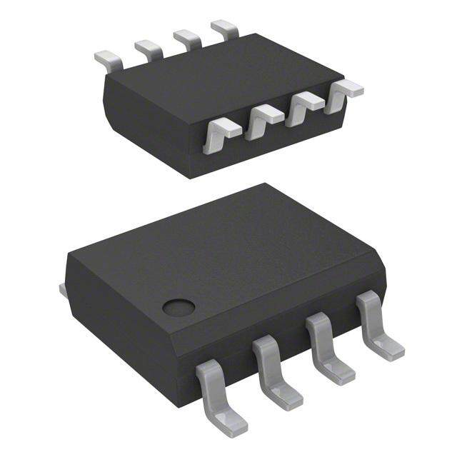
| 描述 | IC LED DRIVER WHITE BCKLGT 6SONLED照明驱动器 White LED Driver |
| 产品分类 | |
| 品牌 | Texas Instruments |
| 产品手册 | |
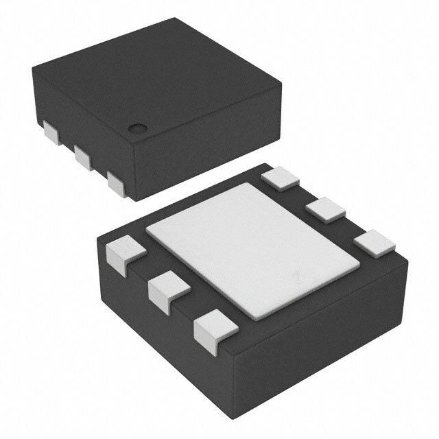
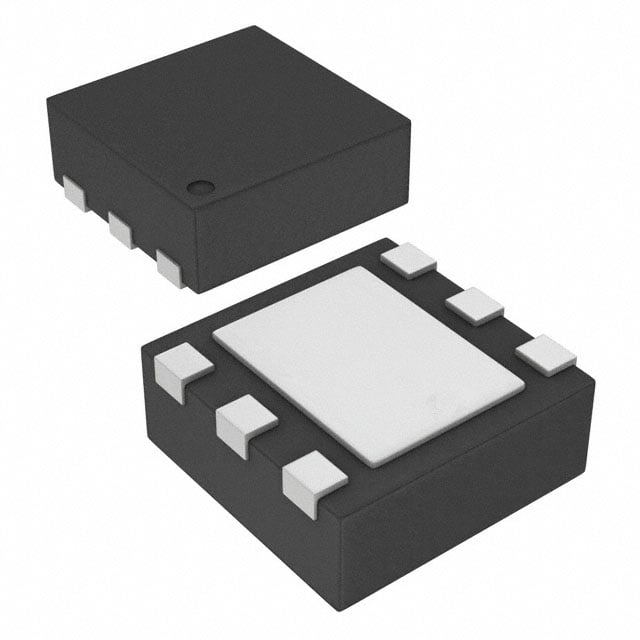
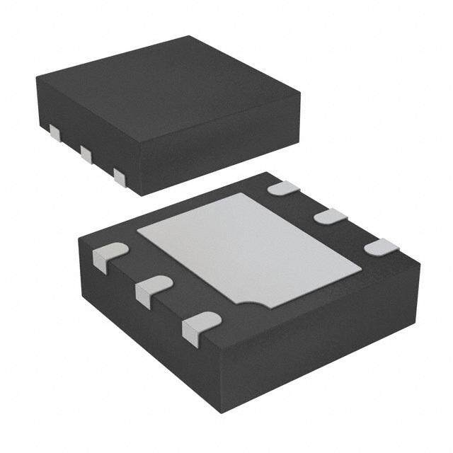
| 产品图片 |
|
| rohs | 符合RoHS无铅 / 符合限制有害物质指令(RoHS)规范要求 |
| 产品系列 | LED照明电子器件,LED照明驱动器,Texas Instruments TPS61160DRVT- |
| 数据手册 | |
| 产品型号 | TPS61160DRVT |
| PCN组件/产地 | |
| 产品种类 | LED照明驱动器 |
| 低电平输出电流 | 100 uA |
| 供应商器件封装 | 6-SON(2x2) |
| 其它名称 | 296-27013-6 |
| 内部驱动器 | 是 |
| 功率耗散 | 1540 mW |
| 包装 | Digi-Reel® |
| 商标 | Texas Instruments |
| 安装类型 | 表面贴装 |
| 安装风格 | SMD/SMT |
| 封装 | Reel |
| 封装/外壳 | 6-WDFN 裸露焊盘 |
| 封装/箱体 | WSON-6 |
| 工作温度 | -40°C ~ 85°C |
| 工作频率 | 600 kHz |
| 工厂包装数量 | 250 |
| 恒压 | - |
| 恒流 | - |
| 拓扑 | PWM,升压(升压) |
| 拓扑结构 | Boost |
| 最大工作温度 | + 85 C |
| 最大电源电流 | 1.8 mA |
| 最小工作温度 | - 40 C |
| 标准包装 | 1 |
| 电压-电源 | 2.7 V ~ 18 V |
| 电压-输出 | 26V |
| 类型 | Inductive |
| 类型-初级 | 背光 |
| 类型-次级 | 白色 LED |
| 系列 | TPS61160 |
| 输入电压 | 2.7 V to 18 V |
| 输出数 | 1 |
| 输出电流 | 700 mA |
| 输出端数量 | 1 Output |
| 输出类型 | Current Mode |
| 配用 | /product-detail/zh/TPS61160EVM-243/296-31227-ND/1907986 |
| 频率 | 500kHz ~ 700kHz |
| 高电平输出电流 | 100 uA |


- 商务部:美国ITC正式对集成电路等产品启动337调查
- 曝三星4nm工艺存在良率问题 高通将骁龙8 Gen1或转产台积电
- 太阳诱电将投资9.5亿元在常州建新厂生产MLCC 预计2023年完工
- 英特尔发布欧洲新工厂建设计划 深化IDM 2.0 战略
- 台积电先进制程称霸业界 有大客户加持明年业绩稳了
- 达到5530亿美元!SIA预计今年全球半导体销售额将创下新高
- 英特尔拟将自动驾驶子公司Mobileye上市 估值或超500亿美元
- 三星加码芯片和SET,合并消费电子和移动部门,撤换高东真等 CEO
- 三星电子宣布重大人事变动 还合并消费电子和移动部门
- 海关总署:前11个月进口集成电路产品价值2.52万亿元 增长14.8%


PDF Datasheet 数据手册内容提取
Product Sample & Technical Tools & Support & Folder Buy Documents Software Community TPS61160,TPS61161 SLVS791E–NOVEMBER2007–REVISEDJULY2016 TPS6116x White LED Drivers With Digital and PWM Brightness Control in 2-mm x 2-mm WSON Package 1 Features The default white LED current is set with the external sensor resistor R , and the feedback voltage is • 2.7-Vto18-VInputVoltageRange SET 1 regulated to 200 mV, as shown in the Typical • 26-VOpenLEDProtection(TPS61160) Application. During the operation, the LED current • 38-VOpenLEDProtection(TPS61161) can be controlled using the one-wire digital interface (EasyScale™ protocol) through the CTRL pin. • 200-mVReferenceVoltageWith ±2%Accuracy Alternatively, a pulse width modulation (PWM) signal • FlexibleDigitalandPWMBrightnessControl can be applied to the CTRL pin through which the • Built-inSoftStart duty cycle determines the feedback reference voltage. In either digital or PWM mode, the • Upto90%Efficiency TPS61160 and TPS61161 do not burst the LED current; therefore, they do not generate audible 2 Applications noises on the output capacitor. For maximum • CellularPhones protection, the device features integrated open LED • PortableMediaPlayers protection that disable the TPS61160 and/or TPS61161 to prevent the output voltage from • UltraMobileDevices exceeding the device's absolute maximum voltage • GPSReceivers ratingsduringopenLEDconditions. • WhiteLEDBacklightingforMediaFormFactor The TPS61160 and TPS61161 are available in a Display space-saving, 2-mm×2-mm WSON package with thermalpad. 3 Description With a 40-V rated integrated switch FET, the DeviceInformation(1) TPS61160 and TPS61161 are boost converters that PARTNUMBER PACKAGE OPENLEDPROTECTION drive LEDs in series. The boost converters run at TPS61160 TPS61160use26V(typical) 600-kHz fixed switching frequency to reduce output WSON(6) TPS61161 TPS61161use38V(typical) ripple, improve conversion efficiency, and allow for theuseofsmallexternalcomponents. (1) For all available packages, see the orderable addendum at theendofthedatasheet. TypicalApplication L1 VI3 V to 18 V 22mH D1 38 V Max C1 C2 1mF TPS61161–Q1 1mF VIN SW ON/OFF DIMMING CTRL FB CONTROL COMP GND R set C3 10W 220 nF L1:TDK VLCF5020T-220MR75-1 C1: Murata GRM188R61E105K C2:Murata GRM21BR71H105K 20 mA D1: ONsemi MBR0540T1 1 An IMPORTANT NOTICE at the end of this data sheet addresses availability, warranty, changes, use in safety-critical applications, intellectualpropertymattersandotherimportantdisclaimers.PRODUCTIONDATA.
TPS61160,TPS61161 SLVS791E–NOVEMBER2007–REVISEDJULY2016 www.ti.com Table of Contents 1 Features.................................................................. 1 8 ApplicationandImplementationInformation... 19 2 Applications........................................................... 1 8.1 ApplicationInformation............................................19 3 Description............................................................. 1 8.2 TypicalApplications ...............................................19 4 RevisionHistory..................................................... 2 9 PowerSupplyRecommendations...................... 28 5 PinConfigurationandFunctions......................... 4 10 Layout................................................................... 29 6 Specifications......................................................... 5 10.1 LayoutGuidelines.................................................29 6.1 AbsoluteMaximumRatings......................................5 10.2 LayoutExample....................................................29 6.2 ESDRatings..............................................................5 10.3 ThermalConsiderations........................................29 6.3 RecommendedOperatingConditions.......................5 11 DeviceandDocumentationSupport................. 30 6.4 ThermalInformation..................................................5 11.1 DeviceSupport......................................................30 6.5 ElectricalCharacteristics...........................................6 11.2 DocumentationSupport........................................30 6.6 TimingRequirements ...............................................7 11.3 RelatedLinks........................................................30 6.7 TypicalCharacteristics..............................................8 11.4 ReceivingNotificationofDocumentationUpdates30 7 DetailedDescription............................................ 11 11.5 CommunityResources..........................................30 7.1 Overview.................................................................11 11.6 Trademarks...........................................................30 7.2 FunctionalBlockDiagram.......................................11 11.7 ElectrostaticDischargeCaution............................30 7.3 FeatureDescription.................................................11 11.8 Glossary................................................................31 7.4 DeviceFunctionalModes........................................13 12 Mechanical,Packaging,andOrderable Information........................................................... 31 7.5 Programming...........................................................15 4 Revision History NOTE:Pagenumbersforpreviousrevisionsmaydifferfrompagenumbersinthecurrentversion. ChangesfromRevisionD(June2015)toRevisionE Page • Changedpackagenamefrom"SON"to"WSON"throughoutdocument.............................................................................. 1 • Deletedthe"Duty"rowstheRecommendedOperatingConditions;added"t "row.................................................... 5 PWM_MIN ChangesfromRevisionC(April2012)toRevisionD Page • AddedPinConfigurationandFunctionssection,ESDRatingtable,FeatureDescription,DeviceFunctionalModes, ApplicationandImplementation,PowerSupplyRecommendations,DosandDon'ts,Layout,Deviceand DocumentationSupport,andMechanical,Packaging,andOrderableInformationsections;changepackagename fromQFNtoSON;removeOrderingInformationtable-infoduplicatedinPOA................................................................... 1 • DeletedDissipationRatingstable-replacedbyupdatedThermalInformation. ................................................................... 5 • Addedparagraphre:notusingEasyScaletochangefeedbackvoltagefrom0mV............................................................ 14 ChangesfromRevisionB(July2011)toRevisionC Page • ChangedtheMaximumdutycycleMINvalueFrom:90%To:93%andtheTYPvalueFrom:93%To:95%...................... 6 • ChangedpositionofV =5VandV =3.6VinFigure3........................................................................................................ 8 I I ChangesfromRevisionA(September2008)toRevisionB Page • ChangedFeaturesitemFrom:26VOpenLEDProtectionfor6LEDs(TPS61160)To:26-VOpenLEDProtection (TPS61160)............................................................................................................................................................................ 1 • ChangedFeaturesitemFrom:38VOpenLEDProtectionfor10LEDs(TPS61161)To:38-VOpenLEDProtection (TPS61161)............................................................................................................................................................................ 1 • ;added38VmaxtoTypicalApplicationdiagram;. ............................................................................................................... 1 • ChangedtheCOMPandCTRLDescriptionintheTerminalFunctionTable......................................................................... 4 • Changedtexttoclarifythe"OpenLEDProtection"description........................................................................................... 12 2 SubmitDocumentationFeedback Copyright©2007–2016,TexasInstrumentsIncorporated ProductFolderLinks:TPS61160 TPS61161
TPS61160,TPS61161 www.ti.com SLVS791E–NOVEMBER2007–REVISEDJULY2016 • ChangedFigure13............................................................................................................................................................... 14 • ChangedtheCOMPENSATIONCAPACITORSELECTIONsection................................................................................... 21 Copyright©2007–2016,TexasInstrumentsIncorporated SubmitDocumentationFeedback 3 ProductFolderLinks:TPS61160 TPS61161
TPS61160,TPS61161 SLVS791E–NOVEMBER2007–REVISEDJULY2016 www.ti.com 5 Pin Configuration and Functions DRVPackage 6-PinWSONwithExposedThermalPad TopView FB VIN Thermal COMP CTRL Pad GND SW PinFunctions PIN I/O DESCRIPTION NAME NO. Outputofthetransconductanceerroramplifier.Connectanexternalcapacitortothispinto COMP 2 O compensatetheconverter. Controlpinoftheboostconverter.Itisamulti-functionalpinwhichcanbeusedforenablecontrol, CTRL 5 I PWManddigitaldimming. FB 1 I Feedbackpinforcurrent.ConnectthesenseresistorfromFBtoGND. GND 3 O Ground Thisistheswitchingnodeofthedevice.ConnecttheinductorbetweentheVINandSWpin.Thispin SW 4 I isalsousedtosensetheoutputvoltageforopenLEDprotection VIN 6 I Theinputsupplypinforthedevice.ConnectVINtoasupplyvoltagebetween2.7Vand18V. Solderthethermalpadtotheanaloggroundplane.Ifpossible,usethermalviatoconnecttoground ThermalPad — — planeforidealpowerdissipation. 4 SubmitDocumentationFeedback Copyright©2007–2016,TexasInstrumentsIncorporated ProductFolderLinks:TPS61160 TPS61161
TPS61160,TPS61161 www.ti.com SLVS791E–NOVEMBER2007–REVISEDJULY2016 6 Specifications 6.1 Absolute Maximum Ratings overoperatingfree-airtemperaturerange(unlessotherwisenoted) (1) MIN MAX UNIT SupplyvoltagesonVIN(2) –0.3 20 V VoltagesonCTRL(2) –0.3 20 V V I VoltageonFBandCOMP(2) –0.3 3 V VoltageonSW(2) –0.3 40 V T Operatingjunctiontemperature 40 150 °C J T Storagetemperature –65 150 °C stg (1) StressesbeyondthoselistedunderAbsoluteMaximumRatingsmaycausepermanentdamagetothedevice.Thesearestressratings only,whichdonotimplyfunctionaloperationofthedeviceattheseoranyotherconditionsbeyondthoseindicatedunderRecommended OperatingConditions.Exposuretoabsolute-maximum-ratedconditionsforextendedperiodsmayaffectdevicereliability. (2) Allvoltagevaluesarewithrespecttonetworkgroundpin. 6.2 ESD Ratings VALUE UNIT Electrostatic Human-bodymodel(HBM),perANSI/ESDA/JEDECJS-001(1) ±4000 V V (ESD) discharge Charged-devicemodel(CDM),perJEDECspecificationJESD22-C101(2) ±1000 (1) JEDECdocumentJEP155statesthat500-VHBMallowssafemanufacturingwithastandardESDcontrolprocess. (2) JEDECdocumentJEP157statesthat250-VCDMallowssafemanufacturingwithastandardESDcontrolprocess. 6.3 Recommended Operating Conditions MIN NOM MAX UNIT V Inputvoltage 2.7 18 V I V Outputvoltage V 38 V O IN L Inductor(1) 10 22 μH ƒ PWMdimmingfrequency 5 100 kHz dim t MinimumpulsewidthatPWMinput 50 ns PWM_MIN C Inputcapacitor 1 μF IN C Outputcapacitor(1) 0.47 10 μF O T Operatingambienttemperature –40 85 °C A T Operatingjunctiontemperature –40 125 °C J (1) Thesevaluesarerecommendedvaluesthathavebeensuccessfullytestedinseveralapplications.Othervaluesmaybeacceptablein otherapplicationsbutshouldbefullytestedbytheuser. 6.4 Thermal Information TPS61160, TPS61161 THERMALMETRIC(1) UNIT DRV(WSON) 6PINS R Junction-to-ambientthermalresistance 96.1 °C/W θJA R Junction-to-case(top)thermalresistance 89 °C/W θJC(top) R Junction-to-boardthermalresistance 65.9 °C/W θJB ψ Junction-to-topcharacterizationparameter 3.2 °C/W JT ψ Junction-to-boardcharacterizationparameter 66.3 °C/W JB R Junction-to-case(bottom)thermalresistance 40.8 °C/W θJC(bot) (1) Formoreinformationabouttraditionalandnewthermalmetrics,seeSemiconductorandICPackageThermalMetrics. Copyright©2007–2016,TexasInstrumentsIncorporated SubmitDocumentationFeedback 5 ProductFolderLinks:TPS61160 TPS61161
TPS61160,TPS61161 SLVS791E–NOVEMBER2007–REVISEDJULY2016 www.ti.com 6.5 Electrical Characteristics V =3.6V,CTRL=V ,T =–40°Cto+85°C,typicalvaluesareatT =25°C(unlessotherwisenoted). IN IN A A PARAMETER TESTCONDITIONS MIN TYP MAX UNIT SUPPLYCURRENT V Inputvoltage 2.7 18 V I I OperatingquiescentcurrentintoVIN DevicePWMswitchingnoload 1.8 mA Q I Shutdowncurrent CRTL=GND,V =4.2V 1 μA SD IN UVLO Undervoltagelockoutthreshold V falling 2.2 2.5 V IN V Undervoltagelockouthysterisis 70 mV hys ENABLEANDREFERENCECONTROL V CTRLlogichighvoltage V =2.7Vto18V 1.2 V (CTRLh) IN V CTRLlogiclowvoltage V =2.7Vto18V 0.4 V (CTRLl) IN R CTRLpulldownresistor 400 800 1600 kΩ (CTRL) VOLTAGEANDCURRENTCONTROL V Voltagefeedbackregulationvoltage 196 200 204 mV REF Voltagefeedbackregulationvoltage V =50mV 47 50 53 FB V(REF_PWM) underbrightnesscontrol mV V =20mV 17 20 23 FB I Voltagefeedbackinputbiascurrent V =200mV 2 μA FB FB ƒ Oscillatorfrequency 500 600 700 kHz S V =100mV,measuredonthe D Maximumdutycycle FB 93% 95% max drivesignaloftheswitchingFET t Minimumonpulsewidth 40 ns min_on I Comppinsinkcurrent 100 μA sink I Comppinsourcecurrent 100 μA source G Erroramplifiertransconductance 240 320 400 μmho ea R Erroramplifieroutputresistance 6 MΩ ea ƒ Erroramplifiercrossoverfrequency 5pFconnectedtoCOMP 500 kHz ea POWERSWITCH V =3.6V 0.3 0.6 IN R N-channelMOSFETon-resistance Ω DS(on) V =3V 0.7 IN I N-channelleakagecurrent V =35V,T =25°C 1 μA LN_NFET SW A 6 SubmitDocumentationFeedback Copyright©2007–2016,TexasInstrumentsIncorporated ProductFolderLinks:TPS61160 TPS61161
TPS61160,TPS61161 www.ti.com SLVS791E–NOVEMBER2007–REVISEDJULY2016 Electrical Characteristics (continued) V =3.6V,CTRL=V ,T =–40°Cto+85°C,typicalvaluesareatT =25°C(unlessotherwisenoted). IN IN A A PARAMETER TESTCONDITIONS MIN TYP MAX UNIT OCandOLP I N-ChannelMOSFETcurrentlimit D=D 0.56 0.7 0.84 A LIM max I Startupcurrentlimit D=D 0.4 A LIM_Start max t Timestepforhalfcurrentlimit 5 ms Half_LIM MeasuredontheSWpin, 25 26 27 V OpenLEDprotectionthreshold TPS61160 37 38 39 V ovp TPS61161 MeasuredontheFBpin, V OpenLEDprotectionthresholdonFB percentageofV 50% (FB_OVP) REF V =200mVand20mV REF V Acknowledgeoutputvoltagelow Opendrain,R =15kΩtoV 0.4 V ACKNL pullup IN THERMALSHUTDOWN T Thermalshutdownthreshold 160 °C shutdown T Thermalshutdownthresholdhysteresis 15 °C hysteresis 6.6 Timing Requirements MIN NOM MAX UNIT OCandOLP t V filtertimeconstant 180 μs REF REF t V rampuptime 213 μs step REF EasyScale t Acknowledgevalidtime(1) 2 μs valACKN t Durationofacknowledgecondition(1) 512 μs ACKN t CTRLpulsewidthtoshutdown,CTRLhightolow 2.5 ms off t EasyScaledetectiontime(2) 260 μs es_det t EasyScaledetectiondelay,MeasuredfromCTRLhigh 100 μs es_delay t EasyScaledetectionwindowtime 1 ms es_win t Starttimeofprogramstream 2 μs START t Endtimeofprogramstream 2 360 μs EOS t Hightimelowbit,logic0 2 180 μs H_LB t Lowtimelowbit,logic0 2×t 360 μs L_LB H_LB t Hightimehighbit,logic1 2×t 360 μs H_HB L_HB t Lowtimehighbit,logic1 2 180 μs L_HB (1) Acknowledgeconditionactive0,thisconditionwillonlybeappliedincasetheRFAbitisset.Opendrainoutput,lineneedstobepulled highbythehostwithresistorload. (2) ToselectEasyScalemode,theCTRLpinhastobelowformorethant duringt . es_det es_win Copyright©2007–2016,TexasInstrumentsIncorporated SubmitDocumentationFeedback 7 ProductFolderLinks:TPS61160 TPS61161
TPS61160,TPS61161 SLVS791E–NOVEMBER2007–REVISEDJULY2016 www.ti.com 6.7 Typical Characteristics 6.7.1 TableOfGraphs FIGURE EfficiencyTPS61160/1 V =3.6V;4,6,8,10LEDs;L=22μH Figure1 IN EfficiencyTPS61160 Figure2 EfficiencyTPS61161 Figure3 Currentlimit T =25°C Figure4 A Currentlimit Figure5 EasyScalestep Figure6 PWMdimminglinearity V =3.6V;PWMFreq=10kHzand40kHz Figure6 IN OutputrippleatPWMdimming 8LEDs;V =3.6V;I =20mA;PWMFreq=10kHz Figure8 IN LOAD Switchingwaveform 8LEDs;V =3.6V;I =20mA;L=22μH Figure9 IN LOAD Start-up 8LEDs;V =3.6V;I =20mA;L=22μH Figure10 IN LOAD OpenLEDprotection 8LEDs;V =3.6V;I =20mA;L=22μH Figure11 IN LOAD 100 100 VI= 3.6 V 4 LEDs 6 LEDs VI= 4.2 V 90 90 80 8 LEDs 80 VI= 3 V Efficiency - %6700 10 LEDs Efficiency - % 6700 VI= 3.6 V 50 48 ((1225..86 VV)),, 160 ( (1392.2 V V) ) LLEEDDss 50 6 LEDs -TPS61160 40 40 0 10 20 30 40 50 0 10 20 30 40 50 Output Current - mA Output Current - mA Figure1. EfficiencyvsOutputCurrent Figure2. EfficiencyvsOutputCurrent 100 1000 VI= 12 V 90 900 mA 800 % 80 VI= 3.6 V VI= 5 V mit - Efficiency - 6700 witch Current Li 567000000 S 50 400 10 LEDs -TPS61161–Q1 40 300 0 10 20 30 40 50 20 30 40 50 60 70 80 90 Output Current - mA Duty Cycle - % Figure3. EfficiencyvsOutputCurrent Figure4. SwitchCurrentLimitvsDutyCycle 8 SubmitDocumentationFeedback Copyright©2007–2016,TexasInstrumentsIncorporated ProductFolderLinks:TPS61160 TPS61161
TPS61160,TPS61161 www.ti.com SLVS791E–NOVEMBER2007–REVISEDJULY2016 1000 200 180 900 160 mA 800 140 witch Current Limit - 567000000 FB Voltage - mV1168020000 S 40 400 20 300 0 -40 -20 0 20 40 60 80 100 120 140 0 2 4 6 8 10 12 14 16 18 20 22 24 26 28 30 32 Temperature -°C Easy Scale Step Step Figure5. SwitchCurrentLimitvsTemperature Figure6. FBVoltagevsEasyScaleStep 200 PWM 2 V/div 10 kHz, 40 kHz 160 V e - m120 VOUT20 mV/divAC g a olt B V 80 F I 10 mA/div LED 40 0 0 20 40 60 80 100 PWM Duty Cycle - % t - 100ms/div Figure7. FBVoltagevsPWMDutyCycle Figure8.OutputRippleAtPWMDimming CTRL 5 V/div SW 20 V/div VOUT 20 mV/div VOUT 10 V/div AC COMP 500 mV/div I L 200 mA/div I L 200 mA/div t - 1ms/div t - 2 ms/div Figure9.SwitchingWaveform Figure10.Start-Up Copyright©2007–2016,TexasInstrumentsIncorporated SubmitDocumentationFeedback 9 ProductFolderLinks:TPS61160 TPS61161
TPS61160,TPS61161 SLVS791E–NOVEMBER2007–REVISEDJULY2016 www.ti.com OPEN LED 5 V/div FB 200 mV/div VOUT 10 V/div I L 200 mA/div t - 100ms/div Figure11.OpenLEDProtection 10 SubmitDocumentationFeedback Copyright©2007–2016,TexasInstrumentsIncorporated ProductFolderLinks:TPS61160 TPS61161
TPS61160,TPS61161 www.ti.com SLVS791E–NOVEMBER2007–REVISEDJULY2016 7 Detailed Description 7.1 Overview The TPS61160 and TPS61161 are high-efficiency, high-output voltage boost converters in a small package size. These devices are ideal for driving white LED in series. The serial LED connection provides even illumination by sourcing the same output current through all LEDs, eliminating the need for expensive factory calibration. Each device integrate a 40-V, 0.7-A switch FET and operatea in pulse width modulation (PWM) with 600-kHz fixed switching frequency. For operation see the block diagram. The duty cycle of the converter is set by the error amplifier output and the current signal applied to the PWM control comparator. The control architecture is based on traditional current-mode control; therefore, a slope compensation is added to the current signal to allow stable operation for duty cycles larger than 50%. The feedback loop regulates the FB pin to a low reference voltage (200mVtypical),reducingthepowerdissipationinthecurrentsenseresistor. 7.2 Functional Block Diagram D1 C2 1 4 Rset FB L1 SW Reference Control Error Amplifer OLP Vin 6 COMP 2 C1 C3 PWM Control Soft 5 Start-up CTRL Ramp Current Generator + Sensor Oscillator GND 3 7.3 Feature Description 7.3.1 SoftStart-Up Soft-start circuitry is integrated into the device to avoid a high inrush current during start-up. After the device is enabled, the voltage at FB pin ramps up to the reference voltage in 32 steps with each step taking 213 μs. This ensures that the output voltage rises slowly to reduce the input current. Additionally, for the first 5 msec after the COMP voltage ramps, the current limit of the switch is set to half of the normal current limit spec. During this period, the input current is kept below 400 mA (typical). See the start-up waveform of a typical example, Figure10. Copyright©2007–2016,TexasInstrumentsIncorporated SubmitDocumentationFeedback 11 ProductFolderLinks:TPS61160 TPS61161
TPS61160,TPS61161 SLVS791E–NOVEMBER2007–REVISEDJULY2016 www.ti.com Feature Description (continued) 7.3.2 OpenLEDProtection Open LED protection circuitry prevents device damage as the result of white LED disconnection. The TPS61160 and TPS61161 monitor the voltage at the SW pin and FB pin during each switching cycle. The circuitry turns off the switch FET and shuts down the device when both of the following conditions persist for 8 switching clock cycles: 1. TheSWvoltageexceedstheV threshold;and OVP 2. TheFBvoltageislessthanhalfofregulationvoltage. As a result, the output voltage falls to the level of the input supply. The device remains in shutdown mode until it is enabled by toggling the CTRL pin logic. To allow the use of inexpensive low-voltage output capacitor, the TPS61160/1 has different open lamp protection thresholds. The threshold is set at 26 V for the TPS61160 and 38 V for the TPS61161. Select the appropriate device so that the product of the number of external LEDs and each LED's maximum forward voltage plus the 200 mV reference voltage does not exceed the minimum OVP thresholdor(n ×V )+200mV≤ V LEDS LED(MAX) OVP(MIN). 7.3.3 CurrentProgram The FB voltage is regulated by a low 0.2-V reference voltage. The LED current is programmed externally using a current-senseresistorinserieswiththeLEDstring.ThevalueoftheR iscalculatedusingEquation1: SET V I FB LED R SET where • I =outputcurrentofLEDs LED • V =regulatedvoltageofFB FB • R =currentsenseresistor (1) SET TheoutputcurrenttolerancedependsontheFBaccuracyandthecurrentsensorresistoraccuracy. 7.3.4 LEDBrightnessDimmingModeSelection The CTRL pin is used for the control input for both dimming modes, PWM dimming and one-wire dimming. The dimming mode for the TPS61160 or TPS61161 is selected each time the device is enabled. The default dimming mode is PWM dimming. To enter the one-wire mode, the following digital pattern on the CTRL pin must be recognizedbythedeviceeverytimethedevicestartsfromtheshutdownmode. 1. PullCTRLpinhightoenabletheTPS61160orTPS61161andtostarttheone-wiredetectionwindow. 2. After the EasyScale detection delay (t , 100 μs) expires, drive CTRL low for more than the EasyScale es_delay detectiontime(t ,260μs). es_detect 3. The CTRL pin has to be low for more than EasyScale detection time before the EasyScale detection window (t ,1msec)expires.EasyScaledetectionwindowstartsfromthefirstCTRLpinlowtohightransition. es_win The device immediately enters the one-wire mode once the above three conditions are met. the EasyScale communication can start before the detection window expires. Once the dimming mode is programmed, it can not be changed without another start-up. This means the device needs to be shutdown by pulling the CTRL low for2.5msandrestarts.SeeFigure12foragraphicalexplanation. 12 SubmitDocumentationFeedback Copyright©2007–2016,TexasInstrumentsIncorporated ProductFolderLinks:TPS61160 TPS61161
TPS61160,TPS61161 www.ti.com SLVS791E–NOVEMBER2007–REVISEDJULY2016 Feature Description (continued) Insert battery PWM signal high CTRL low PWM mode Sdtealratuyp FB ramp Shutdown delay 200mV x duty cycle FB t Insert battery Enter ES mode Enter ES mode Programming Programming code Timing window code high CTRL low ES ES detect time Shutdown mode ES detect delay delay FB ramp FB ramp Programmed value IC (if not programmed,200mV default) Shutdown FB Startup delay 50mV Startup delay 50mV Figure12. DimmingModeDetectionandSoftStartPWMBrightnessDimming 7.3.5 UndervoltageLockout An undervoltage lockout prevents operation of the device at input voltages below typical 2.2 V. When the input voltage is below the undervoltage threshold, the device is shutdown and the internal switch FET is turned off. If theinputvoltagerisesbyundervoltagelockouthysteresis,thedevicerestarts. 7.3.6 ThermalShutdown An internal thermal shutdown turns off the device when the typical junction temperature of 160°C is exceeded. Thedeviceisreleasedfromshutdownautomaticallywhenthejunctiontemperaturedecreasesby15°C. 7.4 Device Functional Modes 7.4.1 Shutdown The TPS61160 or TPS61161 enters shutdown mode when the CTRL voltage is logic low for more than 2.5 ms. During shutdown, the input supply current for the device is less than 1 μA (maximum). Although the internal FET doesnotswitchinshutdown,thereisstillaDCcurrentpathbetweentheinputandtheLEDsthroughtheinductor and Schottky diode. The minimum forward voltage of the LED array must exceed the maximum input voltage to ensure that the LEDs remain off in shutdown. However, in the typical application with two or more LEDs, the forwardvoltageislargeenoughtoreversebiastheSchottkyandkeepleakagecurrentlow. 7.4.2 PWMBrightnessDimming When the CTRL pin is constantly high, the FB voltage is regulated to 200 mV typically. However, the CTRL pin allows a PWM signal to reduce this regulation voltage; therefore, it achieves LED brightness dimming. The relationshipbetweenthedutycycleandFBvoltageisgivenbyEquation2. V Dutyu200mV FB where • Duty=dutycycleofthePWMsignal • 200mV=internalreferencevoltage (2) Copyright©2007–2016,TexasInstrumentsIncorporated SubmitDocumentationFeedback 13 ProductFolderLinks:TPS61160 TPS61161
TPS61160,TPS61161 SLVS791E–NOVEMBER2007–REVISEDJULY2016 www.ti.com Device Functional Modes (continued) As shown in Figure 13, the device chops up the internal 200-mV reference voltage at the duty cycle of the PWM signal. The pulse signal is then filtered by an internal low pass filter. The output of the filter is connected to the error amplifier as the reference voltage for the FB pin regulation. Therefore, although a PWM signal is used for brightness dimming, only the WLED DC current is modulated, which is often referred as analog dimming. This eliminates the audible noise which often occurs when the LED current is pulsed in replica of the frequency and duty cycle of PWM control. Unlike other scheme which filters the PWM signal for analog dimming, TPS61160, TPS61161regulationvoltageisindependentofthePWMlogicvoltagelevelwhichoftenhaslargevariations. For optimum performance, use the PWM dimming frequency in the range of 5 kHz to 100 kHz. The requirement ofminimumdimmingfrequencycomesfromtheEasyScaledetectiondelayanddetectiontimespecificationinthe dimming mode selection. Since the CTRL pin is logic only pin, adding an external RC filter applied to the pin doesnotwork. VBG 200 mV CTRL Error COMP Amplifier FB Figure13. BlockDiagramofProgrammableFBVoltageUsingPWMSignal TouselowerPWMdimming,addanexternalRCnetworkconnectedtotheFBpinasshowninFigure19. 7.4.3 DigitalOne-WireBrightnessDimming The CTRL pin features a simple digital interface to allow digital brightness control. The digital dimming can save the processor power and battery life as it does not require a PWM signal all the time, and the processor can enteridlemodeifavailable. The TPS61160 or TPS61161 adopts the EasyScale protocol for the digital dimming, which can program the FB voltage to any of the 32 steps with single command. The step increment increases with the voltage to produce pseudo logarithmic curve for the brightness step. See the Table 1 for the FB pin voltage steps. The default step is full scale when the device is first enabled (V = 200 mV). The programmed reference voltage is stored in an FB internalregister.Apowerresetclearstheregistervalueandresetittodefault. Do not use EasyScale to change the feedback voltage from 0 mV, effectively disabling the device, to any other voltage. One alternative is to start with V = 10 mV and go to a higher voltage. Another alternative is to disable FB the device by taking the CTRL pin low for 2.5 ms and then re-enter EasyScale to force a soft start from V = 0 FB mVtothedefault200mV. 14 SubmitDocumentationFeedback Copyright©2007–2016,TexasInstrumentsIncorporated ProductFolderLinks:TPS61160 TPS61161
TPS61160,TPS61161 www.ti.com SLVS791E–NOVEMBER2007–REVISEDJULY2016 Device Functional Modes (continued) 7.4.4 ExternalPWMDimming For assistance in selecting the proper values for R , R1-R3, RFLTR, CFLTR and D2 for the specific SET application, refer to How to Use Analog Dimming With the TPS6116x (SLVA471) and/or Design Tool for Analog DimmingUsingaPWMSignal(SLVC366).AlsoseeChoosingComponentValues. 7.5 Programming 7.5.1 EasyScale:One-WireDigitalDimming EasyScale is a simple but flexible one pin interface to configure the FB voltage. The interface is based on a master-slave structure, where the master is typically a microcontroller or application processor. Figure 14 and Table2giveanoverviewoftheprotocol.Theprotocolconsistsofadevicespecificaddressbyteandadatabyte. The device specific address byte is fixed to 72 hex. The data byte consists of five bits for information, two address bits, and the RFA bit. The RFA bit set to high indicates the Request for Acknowledge condition. The Acknowledge condition is only applied if the protocol was received correctly. The advantage of EasyScale compared with other one-pin interfaces is that its bit detection is in a large extent independent from the bit transmissionrate.Itcanautomaticallydetectbitratesfrom1.7kBit/secandupto160kBit/sec. Copyright©2007–2016,TexasInstrumentsIncorporated SubmitDocumentationFeedback 15 ProductFolderLinks:TPS61160 TPS61161
TPS61160,TPS61161 SLVS791E–NOVEMBER2007–REVISEDJULY2016 www.ti.com Table1.SelectableFBVoltages(1) FBvoltage D4 D3 D2 D1 D0 (mV) 0 0 0 0 0 0 0 1 5 0 0 0 0 1 2 8 0 0 0 1 0 3 11 0 0 0 1 1 4 14 0 0 1 0 0 5 17 0 0 1 0 1 6 20 0 0 1 1 0 7 23 0 0 1 1 1 8 26 0 1 0 0 0 9 29 0 1 0 0 1 10 32 0 1 0 1 0 11 35 0 1 0 1 1 12 38 0 1 1 0 0 13 44 0 1 1 0 1 14 50 0 1 1 1 0 15 56 0 1 1 1 1 16 62 1 0 0 0 0 17 68 1 0 0 0 1 18 74 1 0 0 1 0 19 80 1 0 0 1 1 20 86 1 0 1 0 0 21 92 1 0 1 0 1 22 98 1 0 1 1 0 23 104 1 0 1 1 1 24 116 1 1 0 0 0 25 128 1 1 0 0 1 26 140 1 1 0 1 0 27 152 1 1 0 1 1 28 164 1 1 1 0 0 29 176 1 1 1 0 1 30 188 1 1 1 1 0 31 200 1 1 1 1 1 (1) SeeDigitalOne-WireBrightnessDimming. DATAIN DeviceAddress DATABYTE SSttaarrtt DA7 DA6 DA5 DA4 DA3 DA2 DA1 DA0 EOS Start RFA A1 A0 D4 D3 D2 D1 D0 EOS 0 1 1 1 0 0 1 0 DATAOUT ACK Figure14. EasyScaleProtocolOverview 16 SubmitDocumentationFeedback Copyright©2007–2016,TexasInstrumentsIncorporated ProductFolderLinks:TPS61160 TPS61161
TPS61160,TPS61161 www.ti.com SLVS791E–NOVEMBER2007–REVISEDJULY2016 Table2.EasyScaleBitDescriptions BIT TRANSMISSION BYTE NAME DESCRIPTION NUMBER DIRECTION 7 DA7 0MSBdeviceaddress 6 DA6 1 5 DA5 1 Device Address 4 DA4 1 IN Byte 3 DA3 0 72hex 2 DA2 0 1 DA1 1 0 DA0 0LSBdeviceaddress 7(MSB) RFA Requestforacknowledge.Ifhigh,acknowledgeisappliedbydevice 6 A1 0Addressbit1 5 A0 0Addressbit0 4 D4 Databit4 Databyte IN 3 D3 Databit3 2 D2 Databit2 1 D1 Databit1 0(LSB) D0 Databit0 Acknowledgeconditionactive0,thisconditionwillonlybeappliedincaseRFAbitis set.Opendrainoutput,Lineneedstobepulledhighbythehostwithapullup ACK OUT resistor.Thisfeaturecanonlybeusedifthemasterhasanopendrainoutputstage. IncaseofapushpulloutputstageAcknowledgeconditionmaynotberequested! Easy Scale Timing, without acknowledge RFA= 0 tStart Address Byte tStart DATAByte DATAIN Static High Static High DA7 DA0 RFA D0 0 0 T 0 1 T EOS EOS Easy Scale Timing, with acknowledge RFA= 1 tStart Address Byte tStart DATAByte DATAIN Static High Static High DA7 DA0 RFA D0 0 0 TEOS 1 1 tvalACK Acknowledge true, Data Line ACKN pulled down by t device Controller needs to ACKN DATAOUT Pullup Data Line via a Acknowledge resistor to detectACKN false, no pull down t t t t Low High LOW High Low Bit High Bit (Logic 0) (Logic 1) Figure15. EasyScaleBitCoding Copyright©2007–2016,TexasInstrumentsIncorporated SubmitDocumentationFeedback 17 ProductFolderLinks:TPS61160 TPS61161
TPS61160,TPS61161 SLVS791E–NOVEMBER2007–REVISEDJULY2016 www.ti.com All bits are transmitted MSB first and LSB last. Figure 15 shows the protocol without acknowledge request (Bit RFA = 0) as well as the with acknowledge (Bit RFA = 1) request. Prior to both bytes, device address byte and data byte, a start condition must be applied. For this, the CTRL pin must be pulled high for at least t (2 μs) start before the bit transmission starts with the falling edge. If the CTRL pin is already at high level, no start condition is needed prior to the device address byte. The transmission of each byte is closed with an End-of-Stream conditionforatleastt (2μs). EOS The bit detection is based on a Logic Detection scheme, where the criterion is the relation between t and LOW t .Itcanbesimplifiedto: HIGH HighBit:t >t ,butwitht atleast2× t ,seeFigure15. HIGH LOW HIGH LOW LowBit:t <t ,butwitht atleast2× t ,seeFigure15. HIGH LOW LOW HIGH The bit detection starts with a falling edge on the CTRL pin and ends with the next falling edge. Depending on therelationbetweent andt ,thelogic0or1isdetected. HIGH LOW Theacknowledgeconditionisonlyappliedif: • AcknowledgeisrequestedbyasetRFAbit. • Thetransmitteddeviceaddressmatcheswiththedeviceaddressofthedevice. • 16bitsisreceivedcorrectly. If the device turns on the internal ACKN-MOSFET and pulls the CTRL pin low for the time t , which is 512 μs ACKN maximumthentheAcknowledgeconditionisvalidafteraninternaldelaytimet .Thismeansthattheinternal valACK ACKN-MOSFET is turned on after t , when the last falling edge of the protocol was detected. The master valACK controller keeps the line low in this period. The master device can detect the acknowledge condition with its input by releasing the CTRL pin after t and read back a logic 0. The CTRL pin can be used again after the valACK acknowledgeconditionends. Note that the acknowledge condition may only be requested in case the master device has an open drain output. For a push-pull output stage, the use a series resistor in the CRTL line to limit the current to 500 μA is recommendedtoforsuchcasesas: • anaccidentallyrequestedacknowledge,or • toprotecttheinternalACKN-MOSFET. 18 SubmitDocumentationFeedback Copyright©2007–2016,TexasInstrumentsIncorporated ProductFolderLinks:TPS61160 TPS61161
TPS61160,TPS61161 www.ti.com SLVS791E–NOVEMBER2007–REVISEDJULY2016 8 Application and Implementation Information NOTE Information in the following applications sections is not part of the TI component specification, and TI does not warrant its accuracy or completeness. TI’s customers are responsible for determining suitability of components for their purposes. Customers should validateandtesttheirdesignimplementationtoconfirmsystemfunctionality. 8.1 Application Information The TPS61160 and TPS61161 provide a complete high-performance LED lighting solution for mobile devices supportingasinglestringof6(TPS61160)or10(TPS61161)whiteLEDs. 8.2 Typical Applications 8.2.1 TypicalApplicationofTPS61161 L1 VI3 V to 18 V 22mH D1 38 V Max C1 C2 1mF TPS61161–Q1 1mF VIN SW ON/OFF DIMMING CTRL FB CONTROL COMP GND R set C3 10W 220 nF L1:TDK VLCF5020T-220MR75-1 C1: Murata GRM188R61E105K C2:Murata GRM21BR71H105K 20 mA D1: ONsemi MBR0540T1 Figure16. TypicalApplicationofTPS61161 8.2.1.1 DesignRequirements Examplerequirementsforwhite-LED-driverapplications: Table3.DesignParameters DESIGNPARAMETER EXAMPLEVALUE Inductor 22µH Minimuminputvoltage 3V NumberofseriesLED 10 LEDmaximumforwardvoltage(Vf) 3.2V Schottkydiodeforwardvoltage(Vf) 0.2V Efficiency(η) 85% Switchingfrequency(SW) 600kHz Copyright©2007–2016,TexasInstrumentsIncorporated SubmitDocumentationFeedback 19 ProductFolderLinks:TPS61160 TPS61161
TPS61160,TPS61161 SLVS791E–NOVEMBER2007–REVISEDJULY2016 www.ti.com Applying Equation 3 and Equation 4, when V is 3 V, 10 LEDs output equivalent to V of 32.2 V, the inductor IN OUT is22μH,theSchottkyforwardvoltageis0.2V,themaximumoutputcurrentis47mAintypicalcondition. 8.2.1.2 DetailedDesignProcedure 8.2.1.2.1 MaximumOutputCurrent The overcurrent limit in a boost converter limits the maximum input current and thus maximum input power for a given input voltage. Maximum output power is less than maximum input power due to power conversion losses. Therefore, the current limit setting, input voltage, output voltage and efficiency can all change maximum current output. The current limit clamps the peak inductor current; therefore, the ripple has to be subtracted to derive maximum DC current. The ripple current is a function of switching frequency, inductor value and duty cycle. Equation3andEquation4takeintoaccountofalltheabovefactorsformaximumoutputcurrentcalculation. 1 I P “ § 1 1 •” «LuF u¤ (cid:14) ‚» «‹ S 'VOUT (cid:14)VF (cid:14)VIN VIN„»… where • I =inductorpeak-to-peakripple p • L=inductorvalue • V =Schottkydiodeforwardvoltage f • Fs=switchingfrequency • V =outputvoltageoftheboostconverter.ItisequaltothesumofVFBandthevoltagedropacross out LEDs. (3) § I • V u I (cid:16) P uK IN ¤LIM ‚ ' 2„ I OUT_MAX V OUT where • I =maximumoutputcurrentoftheboostconverter out_max • I =overcurrentlimit lim • η=efficiency (4) For instance, when V is 3 V, 8 LEDs output equivalent to V of 26 V, the inductor is 22 μH, the Schottky IN OUT forward voltage is 0.2 V; and then the maximum output current is 65 mA in typical condition. When V is 5 V, 10 IN LEDs output equivalent to V of 32 V, the inductor is 22 μH, the Schottky forward voltage is 0.2 V; and then OUT themaximumoutputcurrentis85mAintypicalcondition. 8.2.1.2.2 InductorSelection Theselectionoftheinductoraffectssteadystateoperationaswellastransientbehaviorandloopstability.These factors make it the most important component in power regulator design. There are three important inductor specifications, inductor value, DC resistance and saturation current. Considering inductor value alone is not enough. The inductor value determines the inductor ripple current. Choose an inductor that can handle the necessary peak current without saturating, according to half of the peak-to-peak ripple current given by Equation 3, pause theinductorDCcurrentgivenby: V uI I OUT OUT IN_DC V uK IN (5) Inductor values can have ±20% tolerance with no current bias. When the inductor current approaches saturation level, its inductance can decrease 20% to 35% from the 0A value depending on how the inductor vendor defines saturation current. Using an inductor with a smaller inductance value forces discontinuous PWM when the inductor current ramps down to zero before the end of each switching cycle. This reduces the boost converter’s maximum output current, causes large input voltage ripple and reduces efficiency. Large inductance value 20 SubmitDocumentationFeedback Copyright©2007–2016,TexasInstrumentsIncorporated ProductFolderLinks:TPS61160 TPS61161
TPS61160,TPS61161 www.ti.com SLVS791E–NOVEMBER2007–REVISEDJULY2016 provides much more output current and higher conversion efficiency. For these reasons, a 10-μH to 22-μH inductor value range is recommended. A 22-μH inductor optimized the efficiency for most application while maintaining low inductor peak-to-peak ripple. Table 4 lists the recommended inductor for the TPS61160 or TPS61161. When recommending inductor value, the factory has considered –40% and 20% tolerance from its nominalvalue. The TPS61160 and TPS61161 have built-in slope compensation to avoid sub-harmonic oscillation associated with current mode control. If the inductor value is lower than 10 μH, the slope compensation may not be adequate, and the loop can be unstable. Therefore, customers need to verify the inductor in their application if it isdifferentfromtherecommendedvalues. Table4.RecommendedInductorsforTPS61160andTPS61161 L(μH) DCRMAX(Ω) SATURATIONCURRENT(mA) SIZE PARTNUMBER VENDOR (L×W×Hmm) LQH3NPN100NM0 10 0.3 750 3×3×1.5 Murata VLCF5020T-220MR75-1 22 0.4 750 5×5×2.0 TDK CDH3809/SLD 10 0.3 570 4×4×1.0 Sumida A997AS-220M 22 0.4 510 4×4×1.8 TOKO 8.2.1.2.3 SchottkyDiodeSelection The high switching frequency of the TPS61160, TPS61161 demands a high-speed rectification for optimum efficiency. Ensure that the diode average and peak current rating exceeds the average output current and peak inductor current. In addition, the diode’s reverse breakdown voltage must exceed the open LED protection voltage.TheONSemiMBR0540andtheZETEXZHCS400arerecommendedforTPS61160andTPS61161. 8.2.1.2.4 CompensationCapacitorSelection The compensation capacitor C3 (see the Functional Block Diagram), connected from COMP pin to GND, is used to stabilize the feedback loop of the TPS61160, TPS61161. A 220-nF ceramic capacitor for C3 is suitable for mostapplications. 8.2.1.2.5 InputandOutputCapacitorSelection The output capacitor is mainly selected to meet the requirements for the output ripple and loop stability. This ripple voltage is related to the capacitor’s capacitance and its equivalent series resistance (ESR). Assuming a capacitorwithzeroESR,theminimumcapacitanceneededforagivenripplecanbecalculatedby: (V (cid:16)V )I C OUT IN OUT OUT V uF uV OUT S RIPPLE where • V =peak-to-peakoutputripple (6) ripple TheadditionaloutputripplecomponentcausedbyESRiscalculatedusing: V I uR RIPPLE_ESR OUT ESR (7) Due to its low ESR, V can be neglected for ceramic capacitors, but must be considered if tantalum or ripple_ESR electrolyticcapacitorsareused. Care must be taken when evaluating a ceramic capacitor’s derating under DC bias, aging and AC signal. For example, larger form factor capacitors (in 1206 size) have a resonant frequencies in the range of the switching frequency. So the effective capacitance is significantly lower. The DC bias can also significantly reduce capacitance. Ceramic capacitors can loss as much as 50% of its capacitance at its rated voltage. Therefore, leavethemarginonthevoltageratingtoensureadequatecapacitanceattherequiredoutputvoltage. The capacitor in the range of 1 μF to 4.7 μF is recommended for input side. The output requires a capacitor in the range of 0.47 μF to 10 μF. The output capacitor affects the loop stability of the boost regulator. If the output capacitor is below the range, the boost regulator can potentially become unstable. For example, when using an outputcapacitorof0.1 μF,a470-nFcompensationcapacitorhastobeusedfortheloopstable. Copyright©2007–2016,TexasInstrumentsIncorporated SubmitDocumentationFeedback 21 ProductFolderLinks:TPS61160 TPS61161
TPS61160,TPS61161 SLVS791E–NOVEMBER2007–REVISEDJULY2016 www.ti.com Thepopularvendorsforhighvalueceramiccapacitorsare: TDK(http://www.component.tdk.com/components.php) Murata(http://www.murata.com/cap/index.html) 8.2.1.3 ApplicationCurves 100 90 80 %) 70 Y ( 60 C N 50 E CI 40 EFFI 30 VIN = 3.0 V VIN = 3.6 V 20 VIN = 4.2 V 10 VIN = 5.0 V 0 0 10 20 30 40 50 60 70 80 90 100 DIMMING DUTY CYCLE (%) C002 Figure17.EfficiencyvsDimmingDutyCycle Figure18.Start-Upwith10SeriesLEDs(DPWM=100%) 8.2.2 Li-IonDriverfor6WhiteLEDswithExternalPWMDimmingNetwork L1 10mH D1 C1 C2 TPS61160 D2 VIN SW 100Ω ON/OFF DIMMING CTRL FB CONTROL R2 COMP GND C3 R1 220nF RSET R 10W FLTR L1: Murata LQH3NPN100NM0 C1: Murata GRM188R61A105K C C2: Murata GRM188R61E474K FLTR D1: ONsemi MBR0540T1 D2: ONsemi MMSZ4711 Figure19. Li-IonDriverfor6WhiteLEDswithExternalPWMDimming 22 SubmitDocumentationFeedback Copyright©2007–2016,TexasInstrumentsIncorporated ProductFolderLinks:TPS61160 TPS61161
TPS61160,TPS61161 www.ti.com SLVS791E–NOVEMBER2007–REVISEDJULY2016 8.2.2.1 DesignRequirements ExampleparametersforwhiteLEDswithexternalPWMdimming: Table5.DesignParametersforWhiteLEDswithExternalPWMDimming DESIGNPARAMETER EXAMPLEVALUE Inductor 10µH Minimuminputvoltage 3.6V NumberofseriesLED 6 LEDmaximumforwardvoltage(Vf) 3.2V Schottkydiodeforwardvoltage(Vf) 0.2V Efficiency 90% Switchingfrequency(f ) 600kHz SW ExternalPWMoutputvoltage 3V ExternalPWMfrequency 20kHz Applying Equation 3 and Equation 4 when V is 3 V, 6 LEDs output equivalent to V of 19.4 V, the inductor is IN OUT 10μH,theSchottkyforwardvoltageis0.2V,themaximumoutputcurrentis76mAintypicalcondition. 8.2.2.2 DetailedDesignProcedure 8.2.2.2.1 ChoosingComponentValues As per SLVA471, the values of R , C , R , R , and R are determined by the system parameters and FLTR FLTR 1 2 SET error tolerance. The main source of LED current error is leakage current from the FB pin. The error gets worse as the LED current decreases. The error due to leakage current is given by Functional Block Diagram, where the impedance seen by the FB pin has a major impact. To reduce error due to the leakage current, the impedance seen by the FB pin needs to be small. Because R is much smaller than R + R , R must be chosen to be 2 1 FLTR 2 smalltominimizetheimpedanceseenbytheFBpin.Ingeneral,R mustbechosentobe1kΩorless.Ifgreater 2 accuracyatsmallercurrentsisneeded,thenR mustbechosentobeevensmaller. 2 I %error = FB V D ´ V + (1- D)V FB - PWM(H) PWM(L) (R + R )// R R +R 1 FLTR 2 1 FLTR (8) Once R has been chosen, the value of R and R + R can be calculated using Equation 9, Equation 10, 2 SET 1 FLTR Equation 11, and Equation 12. The individual values of R and R can be any combination that sums up to R 1 FLTR 1 +R .Ingeneral,choosingR andR tobethesamevaluegivesaminimumrequirementforC . FLTR 1 FLTR FLTR V =D V +(1 - D )V PWM(min) (min) PWM(H) (min) PWM(L) (9) V = D V +(1 - D )V PWM(max) (max) PWM(H) (max) PWM(L) (10) ( ) V V - V FB PWM(max) PWM(min) R = SET V I V I +V I - V I PWM(max)LED(max) FBLED(max) FBLED(min) PWM(min)LED(min) (11) R (I (V - V ) - I (V - V )) V - V 2 LED(max) PWM(max) FB LED(min) PWM(min) FB PWM(max) PWM(min) R + R = + 1 FLTR V (I - I ) I - I FB LED(max) LED(min) LED(max) LED(min) (12) Finally, C can be chosen based on the amount of filtering desired or to provide a gradual dimming effect that FLTR is popular in many lighting products. At a minimum, C must be chosen to provide at least 20 dB of FLTR attenuation at the PWM frequency. Equation 13 can be used to calculate the minimum capacitor value to provide thisattenuation. 1 C = FLTR f 2p(R //R ) pwm FLTR 1 10 (13) Copyright©2007–2016,TexasInstrumentsIncorporated SubmitDocumentationFeedback 23 ProductFolderLinks:TPS61160 TPS61161
TPS61160,TPS61161 SLVS791E–NOVEMBER2007–REVISEDJULY2016 www.ti.com To provide gradual dimming, a large capacitor must be chosen to provide a long transient time when changing the PWM duty cycle. Equation 14 shows how to calculate the recommended corner frequency of the RC filter basedonthe10%to90%risetime.Oncethecornerfrequencyisknown,itcanbeusedtocalculatetherequired capacitorusingEquation15. 0.35 fRC = t r (14) 1 C = FLTR 2p(R //R ) f FLTR 1 RC (15) For example, a design with R and R equal to 10 kΩ and a desired rise time of 500 ms requires a corner FLTR 1 frequencyof0.7Hzandacapacitorof47 μF. 8.2.2.3 ApplicationCurves 100 90 80 %) 70 Y ( 60 C N 50 E CI 40 FFI VIN = 3.0 V E 30 VIN = 3.6 V 20 VIN = 4.2 V 10 VIN = 5.0 V 0 0 10 20 30 40 50 60 70 80 90 100 DIMMING DUTY CYCLE (%) C002 Figure20.EfficiencyvsDimmingDutyCycle Figure21.Start-Upwith6SeriesLEDs(ExternalPWM, D =50%) PWM Figure22.Start-Upwith6SeriesLEDs(ExternalPWM,D =100%) PWM 24 SubmitDocumentationFeedback Copyright©2007–2016,TexasInstrumentsIncorporated ProductFolderLinks:TPS61160 TPS61161
TPS61160,TPS61161 www.ti.com SLVS791E–NOVEMBER2007–REVISEDJULY2016 8.2.3 Li-IonDriverfor6WhiteLEDs L1 V 3 V to 5 V 10mH D1 IN C1 C2 1mF TPS61160 0.47mF VIN SW ON/OFF DIMMING CTRL FB CONTROL COMP GND RSET 20mA C3 10W 220nF L1: Murata LQH3NPN100NM0 C1: Murata GRM188R61A105K C2: Murata GRM188R61E474K D1: ONsemi MBR0540T1 Figure23. Li-IonDriverfor6WhiteLEDs 8.2.3.1 DesignRequirements ExampleparametersforLi-Iondriverswith6whiteLEDs: Table6.DesignParametersforLi-IonDriverwith6WhiteLEDs DESIGNPARAMETER EXAMPLEVALUE Inductor 10µH Minimuminputvoltage 3V NumberofseriesLED 6 LEDmaximumforwardvoltage(Vf) 3.2V Schottkydiodeforwardvoltage(Vf) 0.6V Efficiency(η) 88% Switchingfrequency 600kHz Applying Equation 3 and Equation 4, when V is 3 V, 6 LEDs output equivalent to V of 19.4 V, the inductor is IN OUT 10μH,theSchottkyforwardvoltageis0.2V,themaximumoutputcurrentis66mAintypicalcondition. 8.2.3.2 DetailedDesignProcedure SeeDetailedDesignProcedure. Copyright©2007–2016,TexasInstrumentsIncorporated SubmitDocumentationFeedback 25 ProductFolderLinks:TPS61160 TPS61161
TPS61160,TPS61161 SLVS791E–NOVEMBER2007–REVISEDJULY2016 www.ti.com 8.2.3.3 ApplicationCurves 100 90 80 %) 70 Y ( 60 C N 50 E CI 40 FFI VIN = 3.0 V E 30 VIN = 3.6 V 20 VIN = 4.2 V 10 VIN = 5.0 V 0 0 10 20 30 40 50 60 70 80 90 100 DIMMING DUTY CYCLE (%) C002 Figure24.EfficiencyvsDutyCycle Figure25.Start-Upwith6SeriesLEDs(D =50%) PWM Figure26.Start-Upwith6SeriesLEDs(D =100%) PWM 8.2.4 Li-IonDriverfor8WhiteLEDs For assistance in selecting the proper values for R , R1-R3, RFLTR, CFLTR and D2 for the specific SET application,refertoSLVA471and/orSLVC366. 26 SubmitDocumentationFeedback Copyright©2007–2016,TexasInstrumentsIncorporated ProductFolderLinks:TPS61160 TPS61161
TPS61160,TPS61161 www.ti.com SLVS791E–NOVEMBER2007–REVISEDJULY2016 L1 Vin 3 V to 5 V 22mH D1 C1 C2 TPS61161 VIN SW ON/OFF DIMMING CTRL FB CONTROL COMP GND Rset 10W C3 220 nF L1:TDK VLCF5020T-220MR75-1 20mA C1: Murata GRM188R61A105K C2:Murata GRM21BR71H105K D1: ONsemi MBR0540T1 Figure27. Li-IonDriverfor8WhiteLEDs 8.2.4.1 DesignRequirements ExampleparametersforLi-Iondriverwith8whiteLEDs: Table7.DesignParametersforLi-IonDriverwith8WhiteLEDs DESIGNPARAMETER EXAMPLEVALUE Inductor 22µH Minimuminputvoltage 3V NumberofseriesLED 8 LEDmaximumforwardvoltage(Vf) 3.2V Schottkydiodeforwardvoltage 0.2V Efficiency(η) 85% Switchingfrequency 600kHz Applying Equation 3 and Equation 4, when V is 3 V, 8 LEDs output equivalent to V of 25.8 V, the inductor is IN OUT 22μH,theSchottkyforwardvoltageis0.2V,themaximumoutputcurrentis60mAintypicalcondition. 8.2.4.2 DetailedDesignProcedure SeeDetailedDesignProcedure. Copyright©2007–2016,TexasInstrumentsIncorporated SubmitDocumentationFeedback 27 ProductFolderLinks:TPS61160 TPS61161
TPS61160,TPS61161 SLVS791E–NOVEMBER2007–REVISEDJULY2016 www.ti.com 8.2.4.3 ApplicationCurves 100 90 80 %) 70 Y ( 60 C N 50 E CI 40 FFI VIN = 3.0 V E 30 VIN = 3.6 V 20 VIN = 4.2 V 10 VIN = 5.0 V 0 0 10 20 30 40 50 60 70 80 90 100 DIMMING DUTY CYCLE (%) C002 Figure28.EfficiencyvsDutyCycle Figure29.Start-Upwith8SeriesLEDs(DPWM=100%) 9 Power Supply Recommendations The TPS61160 and TPS61161 are designed to operate from an input supply range of 2.7 V to 18 V. This input supply must be well regulated and be able to provide the peak current required by the LED configuration and inductorselectedwithoutvoltagedropunderloadtransients(start-uporrapidbrightnesschange).Theresistance of the input supply rail must be low enough such that the input current transient does not cause the TPS61160 and TPS61161 supply voltage to droop more than 5%. Additional bulk decoupling located close to the input capacitor(C )mayberequiredtominimizetheimpactoftheinputsupplyrailresistance. IN 28 SubmitDocumentationFeedback Copyright©2007–2016,TexasInstrumentsIncorporated ProductFolderLinks:TPS61160 TPS61161
TPS61160,TPS61161 www.ti.com SLVS791E–NOVEMBER2007–REVISEDJULY2016 10 Layout 10.1 Layout Guidelines As for all switching power supplies, especially those high frequency and high current ones, layout is an important design step. If layout is not carefully done, the regulator could suffer from instability as well as noise problems. To reduce switching losses, the SW pin rise and fall times are made as short as possible. To prevent radiation of high frequency resonance problems, proper layout of the high frequency switching path is essential. Minimize the length and area of all traces connected to the SW pin and always use a ground plane under the switching regulator to minimize inter-plane coupling. The loop including the PWM switch, Schottky diode, and output capacitor,containshighcurrentrisingandfallinginnanosecondandmustbekeptasshortaspossible.Theinput capacitor must not only be close to the VIN pin, but also to the GND pin in order to reduce the device supply ripple.Figure30showsasamplelayout. 10.2 Layout Example Rset C1 Vin LEDs Out FB Vin L1 CTRL COMP CTRL C3 GND SW C2 GND Minimize the area of this Place enough LEDs IN trace VIAs around thermal pad to enhance thermal performance Figure30. TPS6116xSampleLayout 10.3 Thermal Considerations The maximum device junction temperature should be restricted to 125°C under normal operating conditions. This restriction limits the power dissipation of the TPS61160 or TPS61161. Calculate the maximum allowable dissipation,P ,andkeeptheactualdissipationlessthanorequaltoP .Themaximum-power-dissipation D(max) D(max) limitisdeterminedusingvaluesinEquation16: 125°C-T P = A D(max) R qJA where • T isthemaximumambienttemperaturefortheapplication A • R isthethermalresistancejunction-to-ambientgiveninThermalInformation. (16) θJA The TPS61160 and TSP61161 come in a thermally enhanced WSON package. This package includes a thermal pad that improves the thermal capabilities of the package. The R of the WSON package greatly depends on θJA the PCB layout and thermal pad connection. The thermal pad must be soldered to the analog ground on the PCB.Usingthermalviasunderneaththethermalpadasillustratedinthelayoutexample.Alsoseethe QFN/SON PCBAttachment applicationreport(SLUA271). Copyright©2007–2016,TexasInstrumentsIncorporated SubmitDocumentationFeedback 29 ProductFolderLinks:TPS61160 TPS61161
TPS61160,TPS61161 SLVS791E–NOVEMBER2007–REVISEDJULY2016 www.ti.com 11 Device and Documentation Support 11.1 Device Support 11.1.1 Third-PartyProductsDisclaimer TI'S PUBLICATION OF INFORMATION REGARDING THIRD-PARTY PRODUCTS OR SERVICES DOES NOT CONSTITUTE AN ENDORSEMENT REGARDING THE SUITABILITY OF SUCH PRODUCTS OR SERVICES OR A WARRANTY, REPRESENTATION OR ENDORSEMENT OF SUCH PRODUCTS OR SERVICES, EITHER ALONEORINCOMBINATIONWITHANYTIPRODUCTORSERVICE. 11.2 Documentation Support 11.2.1 RelatedDocumentation Forrelateddocumentation,seethefollowing: • QFN/SONPCBAttachment • HowtoUseAnalogDimmingWiththeTPS6116x • DesignToolforAnalogDimmingUsingaPWMSignal 11.3 Related Links 11.3.1 RelatedLinks Table 8 lists quick access links. Categories include technical documents, support and community resources, toolsandsoftware,andquickaccesstosampleorbuy. Table8.RelatedLinks TECHNICAL TOOLS& SUPPORT& PARTS PRODUCTFOLDER SAMPLE&BUY DOCUMENTS SOFTWARE COMMUNITY TPS61160 Clickhere Clickhere Clickhere Clickhere Clickhere TPS61161 Clickhere Clickhere Clickhere Clickhere Clickhere 11.4 Receiving Notification of Documentation Updates To receive notification of documentation updates, navigate to the device product folder on ti.com. In the upper right corner, click on Alert me to register and receive a weekly digest of any product information that has changed.Forchangedetails,reviewtherevisionhistoryincludedinanyreviseddocument. 11.5 Community Resources The following links connect to TI community resources. Linked contents are provided "AS IS" by the respective contributors. They do not constitute TI specifications and do not necessarily reflect TI's views; see TI's Terms of Use. TIE2E™OnlineCommunity TI'sEngineer-to-Engineer(E2E)Community.Createdtofostercollaboration amongengineers.Ate2e.ti.com,youcanaskquestions,shareknowledge,exploreideasandhelp solveproblemswithfellowengineers. DesignSupport TI'sDesignSupport QuicklyfindhelpfulE2Eforumsalongwithdesignsupporttoolsand contactinformationfortechnicalsupport. 11.6 Trademarks EasyScale,E2EaretrademarksofTexasInstruments. Allothertrademarksarethepropertyoftheirrespectiveowners. 11.7 Electrostatic Discharge Caution Thesedeviceshavelimitedbuilt-inESDprotection.Theleadsshouldbeshortedtogetherorthedeviceplacedinconductivefoam duringstorageorhandlingtopreventelectrostaticdamagetotheMOSgates. 30 SubmitDocumentationFeedback Copyright©2007–2016,TexasInstrumentsIncorporated ProductFolderLinks:TPS61160 TPS61161
TPS61160,TPS61161 www.ti.com SLVS791E–NOVEMBER2007–REVISEDJULY2016 11.8 Glossary SLYZ022—TIGlossary. Thisglossarylistsandexplainsterms,acronyms,anddefinitions. 12 Mechanical, Packaging, and Orderable Information The following pages include mechanical, packaging, and orderable information. This information is the most current data available for the designated devices. This data is subject to change without notice and revision of thisdocument.Forbrowser-basedversionsofthisdatasheet,refertotheleft-handnavigation. Copyright©2007–2016,TexasInstrumentsIncorporated SubmitDocumentationFeedback 31 ProductFolderLinks:TPS61160 TPS61161
PACKAGE OPTION ADDENDUM www.ti.com 6-Feb-2020 PACKAGING INFORMATION Orderable Device Status Package Type Package Pins Package Eco Plan Lead/Ball Finish MSL Peak Temp Op Temp (°C) Device Marking Samples (1) Drawing Qty (2) (6) (3) (4/5) HPA00667DRVR ACTIVE WSON DRV 6 3000 Green (RoHS NIPDAU Level-2-260C-1 YEAR -40 to 85 BZR & no Sb/Br) HPA00810-2/2 ACTIVE WSON DRV 6 3000 Green (RoHS NIPDAU Level-2-260C-1 YEAR -40 to 85 BZR & no Sb/Br) TPS61160DRVR ACTIVE WSON DRV 6 3000 Green (RoHS NIPDAU Level-2-260C-1 YEAR -40 to 85 BZQ & no Sb/Br) TPS61160DRVRG4 ACTIVE WSON DRV 6 3000 Green (RoHS NIPDAU Level-2-260C-1 YEAR -40 to 85 BZQ & no Sb/Br) TPS61160DRVT ACTIVE WSON DRV 6 250 Green (RoHS NIPDAU Level-2-260C-1 YEAR -40 to 85 BZQ & no Sb/Br) TPS61160DRVTG4 ACTIVE WSON DRV 6 250 Green (RoHS NIPDAU Level-2-260C-1 YEAR -40 to 85 BZQ & no Sb/Br) TPS61161DRVR ACTIVE WSON DRV 6 3000 Green (RoHS NIPDAU Level-2-260C-1 YEAR -40 to 85 BZR & no Sb/Br) TPS61161DRVRG4 ACTIVE WSON DRV 6 3000 Green (RoHS NIPDAU Level-2-260C-1 YEAR -40 to 85 BZR & no Sb/Br) TPS61161DRVT ACTIVE WSON DRV 6 250 Green (RoHS NIPDAU Level-2-260C-1 YEAR -40 to 85 BZR & no Sb/Br) TPS61161DRVTG4 ACTIVE WSON DRV 6 250 Green (RoHS NIPDAU Level-2-260C-1 YEAR -40 to 85 BZR & no Sb/Br) (1) The marketing status values are defined as follows: ACTIVE: Product device recommended for new designs. LIFEBUY: TI has announced that the device will be discontinued, and a lifetime-buy period is in effect. NRND: Not recommended for new designs. Device is in production to support existing customers, but TI does not recommend using this part in a new design. PREVIEW: Device has been announced but is not in production. Samples may or may not be available. OBSOLETE: TI has discontinued the production of the device. (2) RoHS: TI defines "RoHS" to mean semiconductor products that are compliant with the current EU RoHS requirements for all 10 RoHS substances, including the requirement that RoHS substance do not exceed 0.1% by weight in homogeneous materials. Where designed to be soldered at high temperatures, "RoHS" products are suitable for use in specified lead-free processes. TI may reference these types of products as "Pb-Free". RoHS Exempt: TI defines "RoHS Exempt" to mean products that contain lead but are compliant with EU RoHS pursuant to a specific EU RoHS exemption. Green: TI defines "Green" to mean the content of Chlorine (Cl) and Bromine (Br) based flame retardants meet JS709B low halogen requirements of <=1000ppm threshold. Antimony trioxide based flame retardants must also meet the <=1000ppm threshold requirement. (3) MSL, Peak Temp. - The Moisture Sensitivity Level rating according to the JEDEC industry standard classifications, and peak solder temperature. Addendum-Page 1
PACKAGE OPTION ADDENDUM www.ti.com 6-Feb-2020 (4) There may be additional marking, which relates to the logo, the lot trace code information, or the environmental category on the device. (5) Multiple Device Markings will be inside parentheses. Only one Device Marking contained in parentheses and separated by a "~" will appear on a device. If a line is indented then it is a continuation of the previous line and the two combined represent the entire Device Marking for that device. (6) Lead/Ball Finish - Orderable Devices may have multiple material finish options. Finish options are separated by a vertical ruled line. Lead/Ball Finish values may wrap to two lines if the finish value exceeds the maximum column width. Important Information and Disclaimer:The information provided on this page represents TI's knowledge and belief as of the date that it is provided. TI bases its knowledge and belief on information provided by third parties, and makes no representation or warranty as to the accuracy of such information. Efforts are underway to better integrate information from third parties. TI has taken and continues to take reasonable steps to provide representative and accurate information but may not have conducted destructive testing or chemical analysis on incoming materials and chemicals. TI and TI suppliers consider certain information to be proprietary, and thus CAS numbers and other limited information may not be available for release. In no event shall TI's liability arising out of such information exceed the total purchase price of the TI part(s) at issue in this document sold by TI to Customer on an annual basis. OTHER QUALIFIED VERSIONS OF TPS61161 : •Automotive: TPS61161-Q1 NOTE: Qualified Version Definitions: •Automotive - Q100 devices qualified for high-reliability automotive applications targeting zero defects Addendum-Page 2
PACKAGE MATERIALS INFORMATION www.ti.com 25-Jan-2017 TAPE AND REEL INFORMATION *Alldimensionsarenominal Device Package Package Pins SPQ Reel Reel A0 B0 K0 P1 W Pin1 Type Drawing Diameter Width (mm) (mm) (mm) (mm) (mm) Quadrant (mm) W1(mm) TPS61160DRVR WSON DRV 6 3000 180.0 8.4 2.3 2.3 1.15 4.0 8.0 Q2 TPS61160DRVT WSON DRV 6 250 180.0 8.4 2.3 2.3 1.15 4.0 8.0 Q2 TPS61161DRVR WSON DRV 6 3000 180.0 8.4 2.3 2.3 1.15 4.0 8.0 Q2 TPS61161DRVT WSON DRV 6 250 180.0 8.4 2.3 2.3 1.15 4.0 8.0 Q2 PackMaterials-Page1
PACKAGE MATERIALS INFORMATION www.ti.com 25-Jan-2017 *Alldimensionsarenominal Device PackageType PackageDrawing Pins SPQ Length(mm) Width(mm) Height(mm) TPS61160DRVR WSON DRV 6 3000 210.0 185.0 35.0 TPS61160DRVT WSON DRV 6 250 210.0 185.0 35.0 TPS61161DRVR WSON DRV 6 3000 210.0 185.0 35.0 TPS61161DRVT WSON DRV 6 250 210.0 185.0 35.0 PackMaterials-Page2
GENERIC PACKAGE VIEW DRV 6 WSON - 0.8 mm max height PLASTIC SMALL OUTLINE - NO LEAD Images above are just a representation of the package family, actual package may vary. Refer to the product data sheet for package details. 4206925/F
PACKAGE OUTLINE DRV0006A WSON - 0.8 mm max height SCALE 5.500 PLASTIC SMALL OUTLINE - NO LEAD B 2.1 A 1.9 PIN 1 INDEX AREA 2.1 1.9 0.8 C 0.7 SEATING PLANE 0.08 C (0.2) TYP 1 0.1 0.05 EXPOSED 0.00 THERMAL PAD 3 4 2X 7 1.3 1.6 0.1 6 1 4X 0.65 0.35 6X PIN 1 ID 0.3 0.25 6X (OPTIONAL) 0.2 0.1 C A B 0.05 C 4222173/B 04/2018 NOTES: 1. All linear dimensions are in millimeters. Any dimensions in parenthesis are for reference only. Dimensioning and tolerancing per ASME Y14.5M. 2. This drawing is subject to change without notice. 3. The package thermal pad must be soldered to the printed circuit board for thermal and mechanical performance. www.ti.com
EXAMPLE BOARD LAYOUT DRV0006A WSON - 0.8 mm max height PLASTIC SMALL OUTLINE - NO LEAD 6X (0.45) (1) 1 7 6X (0.3) 6 SYMM (1.6) (1.1) 4X (0.65) 4 3 (R0.05) TYP SYMM ( 0.2) VIA (1.95) TYP LAND PATTERN EXAMPLE SCALE:25X 0.07 MAX 0.07 MIN ALL AROUND ALL AROUND SOLDER MASK METAL METAL UNDER SOLDER MASK OPENING SOLDER MASK OPENING NON SOLDER MASK DEFINED SOLDER MASK (PREFERRED) DEFINED SOLDER MASK DETAILS 4222173/B 04/2018 NOTES: (continued) 4. This package is designed to be soldered to a thermal pad on the board. For more information, see Texas Instruments literature number SLUA271 (www.ti.com/lit/slua271). 5. Vias are optional depending on application, refer to device data sheet. If some or all are implemented, recommended via locations are shown. www.ti.com
EXAMPLE STENCIL DESIGN DRV0006A WSON - 0.8 mm max height PLASTIC SMALL OUTLINE - NO LEAD SYMM 6X (0.45) METAL 1 7 6X (0.3) 6 (0.45) SYMM 4X (0.65) (0.7) 4 3 (R0.05) TYP (1) (1.95) SOLDER PASTE EXAMPLE BASED ON 0.125 mm THICK STENCIL EXPOSED PAD #7 88% PRINTED SOLDER COVERAGE BY AREA UNDER PACKAGE SCALE:30X 4222173/B 04/2018 NOTES: (continued) 6. Laser cutting apertures with trapezoidal walls and rounded corners may offer better paste release. IPC-7525 may have alternate design recommendations. www.ti.com
IMPORTANTNOTICEANDDISCLAIMER TI PROVIDES TECHNICAL AND RELIABILITY DATA (INCLUDING DATASHEETS), DESIGN RESOURCES (INCLUDING REFERENCE DESIGNS), APPLICATION OR OTHER DESIGN ADVICE, WEB TOOLS, SAFETY INFORMATION, AND OTHER RESOURCES “AS IS” AND WITH ALL FAULTS, AND DISCLAIMS ALL WARRANTIES, EXPRESS AND IMPLIED, INCLUDING WITHOUT LIMITATION ANY IMPLIED WARRANTIES OF MERCHANTABILITY, FITNESS FOR A PARTICULAR PURPOSE OR NON-INFRINGEMENT OF THIRD PARTY INTELLECTUAL PROPERTY RIGHTS. These resources are intended for skilled developers designing with TI products. You are solely responsible for (1) selecting the appropriate TI products for your application, (2) designing, validating and testing your application, and (3) ensuring your application meets applicable standards, and any other safety, security, or other requirements. These resources are subject to change without notice. TI grants you permission to use these resources only for development of an application that uses the TI products described in the resource. Other reproduction and display of these resources is prohibited. No license is granted to any other TI intellectual property right or to any third party intellectual property right. TI disclaims responsibility for, and you will fully indemnify TI and its representatives against, any claims, damages, costs, losses, and liabilities arising out of your use of these resources. TI’s products are provided subject to TI’s Terms of Sale (www.ti.com/legal/termsofsale.html) or other applicable terms available either on ti.com or provided in conjunction with such TI products. TI’s provision of these resources does not expand or otherwise alter TI’s applicable warranties or warranty disclaimers for TI products. Mailing Address: Texas Instruments, Post Office Box 655303, Dallas, Texas 75265 Copyright © 2020, Texas Instruments Incorporated