ICGOO在线商城 > TPS61097-33DBVT
 Datasheet下载
- 型号: TPS61097-33DBVT
- 制造商: Texas Instruments
- 库位|库存: xxxx|xxxx
- 要求:
| 数量阶梯 | 香港交货 | 国内含税 |
| +xxxx | $xxxx | ¥xxxx |
查看当月历史价格
查看今年历史价格
TPS61097-33DBVT产品简介:
ICGOO电子元器件商城为您提供TPS61097-33DBVT由Texas Instruments设计生产,在icgoo商城现货销售,并且可以通过原厂、代理商等渠道进行代购。 提供TPS61097-33DBVT价格参考以及Texas InstrumentsTPS61097-33DBVT封装/规格参数等产品信息。 你可以下载TPS61097-33DBVT参考资料、Datasheet数据手册功能说明书, 资料中有TPS61097-33DBVT详细功能的应用电路图电压和使用方法及教程。
| 参数 | 数值 |
| 产品目录 | 集成电路 (IC)半导体 |
| 描述 | IC REG BST SYNC 3.3V 0.1A SOT23稳压器—开关式稳压器 100mA DC/DC Cnvrtr w/ Lo Quies Crnt |
| 产品分类 | |
| 品牌 | Texas Instruments |
| 产品手册 | |
| 产品图片 |
|
| rohs | 符合RoHS无铅 / 符合限制有害物质指令(RoHS)规范要求 |
| 产品系列 | 电源管理 IC,稳压器—开关式稳压器,Texas Instruments TPS61097-33DBVT- |
| 数据手册 | |
| 产品型号 | TPS61097-33DBVT |
| PCN设计/规格 | |
| PWM类型 | 电流模式 |
| 产品培训模块 | http://www.digikey.cn/PTM/IndividualPTM.page?site=cn&lang=zhs&ptm=25729 |
| 产品目录页面 | |
| 产品种类 | 稳压器—开关式稳压器 |
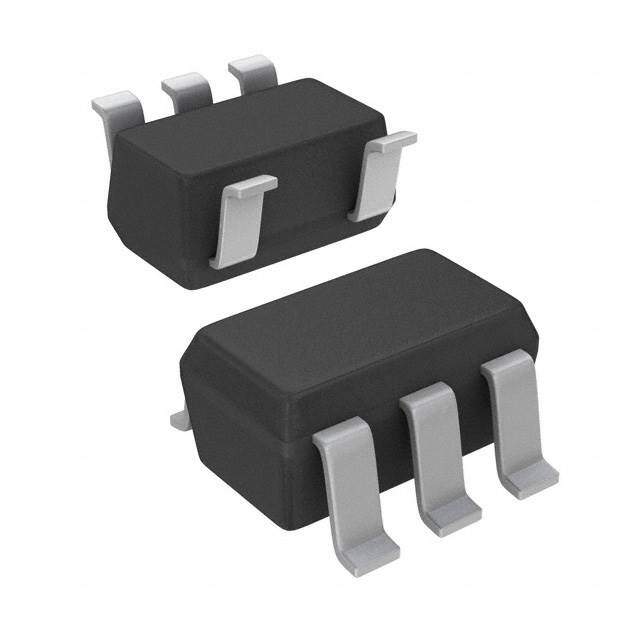
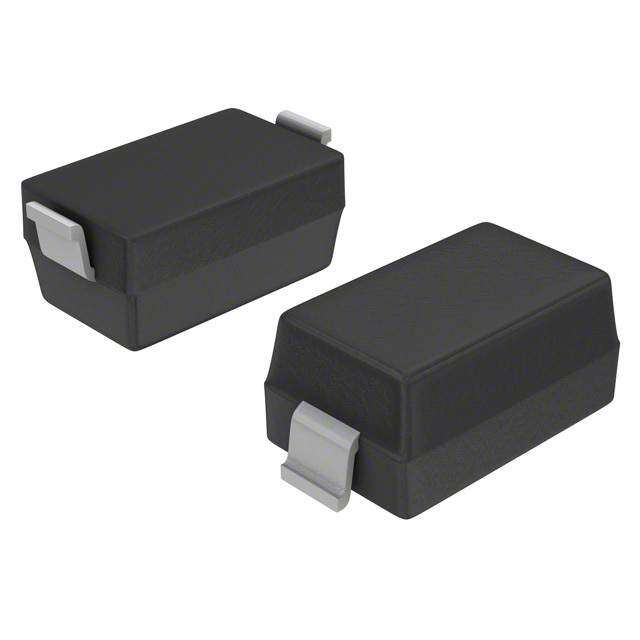
| 供应商器件封装 | SOT-23-5 |
| 其它名称 | 296-24656-2 |
| 制造商产品页 | http://www.ti.com/general/docs/suppproductinfo.tsp?distId=10&orderablePartNumber=TPS61097-33DBVT |
| 包装 | 带卷 (TR) |
| 同步整流器 | 是 |
| 商标 | Texas Instruments |
| 安装类型 | 表面贴装 |
| 安装风格 | SMD/SMT |
| 封装 | Reel |
| 封装/外壳 | SC-74A,SOT-753 |
| 封装/箱体 | SOT-23-5 |
| 工作温度 | -40°C ~ 85°C |
| 工作温度范围 | - 40 C to + 85 C |
| 工厂包装数量 | 250 |
| 开关频率 | - |
| 拓扑结构 | Boost |
| 最大工作温度 | + 85 C |
| 最大输入电压 | 5.5 V |
| 最小工作温度 | - 40 C |
| 最小输入电压 | 0.9 V |
| 标准包装 | 250 |
| 电压-输入 | 0.9 V ~ 5.5 V |
| 电压-输出 | 3.3V |
| 电流-输出 | 100mA |
| 类型 | 升压(升压) |
| 系列 | TPS61097-33 |
| 负载调节 | 0.5 % |
| 输入电压 | 0.9 V to 5.5 V |
| 输出数 | 1 |
| 输出电压 | 3.3 V |
| 输出电流 | 100 mA |
| 输出端数量 | 1 Output |
| 输出类型 | 固定 |
| 配用 | /product-detail/zh/TPS61097-33EVM-498/296-31225-ND/2232826 |
| 频率-开关 | - |


- 商务部:美国ITC正式对集成电路等产品启动337调查
- 曝三星4nm工艺存在良率问题 高通将骁龙8 Gen1或转产台积电
- 太阳诱电将投资9.5亿元在常州建新厂生产MLCC 预计2023年完工
- 英特尔发布欧洲新工厂建设计划 深化IDM 2.0 战略
- 台积电先进制程称霸业界 有大客户加持明年业绩稳了
- 达到5530亿美元!SIA预计今年全球半导体销售额将创下新高
- 英特尔拟将自动驾驶子公司Mobileye上市 估值或超500亿美元
- 三星加码芯片和SET,合并消费电子和移动部门,撤换高东真等 CEO
- 三星电子宣布重大人事变动 还合并消费电子和移动部门
- 海关总署:前11个月进口集成电路产品价值2.52万亿元 增长14.8%


PDF Datasheet 数据手册内容提取
Not Recommended for New Designs – see TPS61097A-33 TPS61097 www.ti.com SLVS872C–JUNE2009–REVISEDDECEMBER2011 LOW INPUT VOLTAGE SYNCHRONOUS BOOST CONVERTER WITH LOW QUIESCENT CURRENT CheckforSamples:TPS61097 FEATURES 1 • Upto95%EfficiencyatTypicalOperating APPLICATIONS Conditions • MSP430Applications • ConnectionfromBatterytoLoadviaBypass • AllSingle-Cell,Two-Cell,andThree-Cell SwitchinShutdownMode Alkaline,NiCd,NiMH,orSingle-CellLi-Battery • TypicalShutdownCurrentLessThan5nA PoweredProducts • TypicalQuiescentCurrentLessThan5μA • PersonalMedicalProducts • OperatingInputVoltageRange • FuelCellandSolarCellPoweredProducts From0.9Vto5.5V • PDAs • Power-SaveModeforImprovedEfficiencyat • MobileApplications LowOutputPower • WhiteLEDs • OvertemperatureProtection • Small2.8-mmx2.9-mm5-PinSOT-23Package (6-PinforAdjustable) DESCRIPTION The TPS61097 provide a power supply solution for products powered by either a single-cell, two-cell, or three-cell alkaline, NiCd, or NiMH, or one-cell Li-Ion or Li-polymer battery. They can also be used in fuel cell or solar cell powered devices where the capability of handling low input voltages is essential. Possible output currents depend on the input-to-output voltage ratio. The devices provides output currents up to 100 mA at a 3.3-V output while using a single-cell Li-Ion or Li-Polymer battery. The boost converter is based on a current-mode controller using synchronous rectification to obtain maximum efficiency. The maximum average input current is limited to a value of 350 mA. The output voltage can be programmed by an external resistor divider, or it is fixed internally on the chip. The converter can be disabled to minimize battery drain. During shutdown, the battery is connected to the load to enable battery backup of critical functions on the load. The fixedoutputdeviceispackagedina5-pinSOT-23package(DBV)measuring2.8mm×2.9mm. TPS61097-33 V L VOUT OUT L1 +3.3V C2 V IN VIN 0.9 V to 3.3V C1 EN GND 1 Pleasebeawarethatanimportantnoticeconcerningavailability,standardwarranty,anduseincriticalapplicationsofTexas Instrumentssemiconductorproductsanddisclaimerstheretoappearsattheendofthisdatasheet. UNLESS OTHERWISE NOTED this document contains Copyright©2009–2011,TexasInstrumentsIncorporated PRODUCTION DATA information current as of publication date. Products conform to specifications per the terms of Texas Instruments standard warranty. Production processing does not necessarilyincludetestingofallparameters.
TPS61097 Not Recommended for New Designs – see TPS61097A-33 SLVS872C–JUNE2009–REVISEDDECEMBER2011 www.ti.com ORDERINGINFORMATION (1) (2) T PACKAGE(3) ORDERABLEPARTNUMBER TOP-SIDEMARKING A Reelof3000 TPS61097-33DBVR –40°Cto85°C 5-pinSOT-23–DBV NFSK Reelof250 TPS61097-33DBVT (1) Forthemostcurrentpackageandorderinginformation,seethePackageOptionAddendumattheendofthisdocument,orseetheTI websiteatwww.ti.com. (2) Contactthefactoryforavailabilityofotherfixedoutputvoltageversions. (3) Packagedrawings,thermaldata,andsymbolizationareavailableatwww.ti.com/packaging. ABSOLUTE MAXIMUM RATINGS overoperatingfree-airtemperaturerange(unlessotherwisenoted)(1) V Inputvoltagerange VIN,L,VOUT,EN,FB –0.3Vto7V I I Short-circuitcurrent 400mA sc T Junctiontemperaturerange –40°Cto150°C J T Storagetemperaturerange –65°Cto150°C stg ESD Electrostaticdischargerating Human-BodyModel(HBM) (2) 2000V (1) StressesbeyondthoselistedunderAbsoluteMaximumRatingsmaycausepermanentdamagetothedevice.Thesearestressratings only,andfunctionaloperationofthedeviceattheseoranyotherconditionsbeyondthoseindicatedunderRecommendedOperating Conditionsisnotimplied.Exposuretoabsolute-maximum-ratedconditionsforextendedperiodsmayaffectdevicereliability. (2) ESDtestingisperformedaccordingtotherespectiveJESD22JEDECstandard. DISSIPATION RATINGS TABLE THERMALRESISTANCE POWERRATING DERATINGFACTORABOVE PACKAGE θ T ≤25°C T =25°C JA A A DBV 255°C/W 390mW -3.92mW/°C RECOMMENDED OPERATING CONDITIONS MIN MAX UNIT V SupplyvoltageatVIN 0.9 5.5 V IN V Adjustableoutputvoltage 1.8 5.5 V OUT T Operatingfreeairtemperaturerange –40 85 °C A T Operatingjunctiontemperaturerange –40 125 °C J 2 SubmitDocumentationFeedback Copyright©2009–2011,TexasInstrumentsIncorporated
Not Recommended for New Designs – see TPS61097A-33 TPS61097 www.ti.com SLVS872C–JUNE2009–REVISEDDECEMBER2011 ELECTRICAL CHARACTERISTICS overrecommendedfree-airtemperaturerangeandoverrecommendedinputvoltagerange(typicalatanambienttemperature rangeof25°C)(unlessotherwisenoted) DC/DCSTAGE PARAMETER TESTCONDITIONS MIN TYP MAX UNIT V Inputvoltage 0.9 5.5 V IN V TPS61097-33 V =1.2V,I =10mA 3.20 3.30 3.40 V OUT IN OUT I Switchcurrentlimit V =3.3V 200 350 475 mA SW OUT Rectifyingswitchonresistance V =3.3V 1.0 Ω OUT Mainswitchonresistance V =3.3V 1.0 Ω OUT Bypassswitchonresistance V =1.2I =100mA 3.4 Ω IN OUT Lineregulation V <V ,V =1.2Vto1.8V,I =10mA 0.5% IN OUT IN OUT Loadregulation V <V ,I =10mAto50mA,V =1.8V 0.5% IN OUT OUT IN V 1 2.5 μA IN I Quiescentcurrent I =0mA,V =V =1.2V,V =3.4V Q O EN IN OUT V 4 6.5 μA OUT V =0V,V =1.2V,I =0mA 0.005 0.15 EN IN OUT I Shutdowncurrent V μA SD IN V =0V,V =3V,I =0mA 0.005 0.15 EN IN OUT LeakagecurrentintoL V =0V,V =1.2V,V =1.2V 0.01 1 μA EN IN L CONTROLSTAGE PARAMETER TESTCONDITIONS MIN TYP MAX UNIT ENinputcurrent EN=0VorEN=V 0.01 0.1 μA IN V Logiclowlevel,ENfallingedge 0.65 V IL VIN+ V Logichighlevel,ENrisingedge 0.78 V IH 1.0V Overtemperatureprotection 150 °C Overtemperaturehysteresis 20 °C VUVLO Undervoltagelock-outthresholdforturnoff VINdecreasing 0.5 0.7 Copyright©2009–2011,TexasInstrumentsIncorporated SubmitDocumentationFeedback 3
TPS61097 Not Recommended for New Designs – see TPS61097A-33 SLVS872C–JUNE2009–REVISEDDECEMBER2011 www.ti.com PIN ASSIGNMENTS FIXED OUTPUTVOLTAGE DBV PACKAGE (TOPVIEW) VIN 1 5 L GGNNDD 2 EN 3 4 VOUT TerminalFunctions TERMINAL NO. I/O DESCRIPTION NAME Fixed VIN 1 I Boostconverterinputvoltage GND 2 Control/logicground EN 3 I Enableinput(1=enabled,0=disabled).ENmustbeactivelyterminatedhighorlow. VOUT 4 O Boostconverteroutput L 5 I Connectionforinductor FB – I Voltagefeedback 4 SubmitDocumentationFeedback Copyright©2009–2011,TexasInstrumentsIncorporated
Not Recommended for New Designs – see TPS61097A-33 TPS61097 www.ti.com SLVS872C–JUNE2009–REVISEDDECEMBER2011 FUNCTIONALBLOCKDIAGRAM(FIXEDOUTPUTVERSION) Bypass Switch P N L VOUT Rectifying Switch Thermal Shutdown Startup Circuit Driver N VIN Main Undervoltage Control Logic Switch Lockout Current Bypass Switch Sense Control EN Overvoltage Protection GND 1.20 V Copyright©2009–2011,TexasInstrumentsIncorporated SubmitDocumentationFeedback 5
TPS61097 Not Recommended for New Designs – see TPS61097A-33 SLVS872C–JUNE2009–REVISEDDECEMBER2011 www.ti.com PARAMETER MEASUREMENT INFORMATION TPS61097-33 V L VOUT OUT L1 +3.3V C2 V IN VIN 0.9 V to 3.3V C1 EN GND C1 10μF C2 10μF L 10μH Table1.ListofComponents REFERENCE MANUFACTURER PARTNO. C1 Murata GRM319R61A106KE1910μF10VX5R120620% C2 Murata GRM319R61A106KE1910μF10VX5R120620% L1 Coilcraft DO3314-103MLC 6 SubmitDocumentationFeedback Copyright©2009–2011,TexasInstrumentsIncorporated
Not Recommended for New Designs – see TPS61097A-33 TPS61097 www.ti.com SLVS872C–JUNE2009–REVISEDDECEMBER2011 TYPICAL CHARACTERISTICS Table2.TableofGraphs FIGURE MaximumOutputCurrent vsInputVoltage 1 vsOutputCurrent 2 Efficiency vsInputVoltage 3 vsInputVoltage(DeviceEnabled,NoOutputLoad,V =3.3V) 4 OUT InputCurrent vsInputVoltage(DeviceDisabled,NoOutputLoad) 5 vsTemperature 6 StartupVoltage vsOutputCurrent 7 vsOutputCurrent 8 OutputVoltage vsInputVoltage 9 OutputVoltageRipple 10 LoadTransientResponse 11 LineTransientResponse 12 Waveforms SwitchingWaveform,ContinuousMode 13 SwitchingWaveform,DiscontinuousMode 14 StartupAfterEnable(V =1.2V,I =10mA) 15 IN OUT StartupAfterEnable(V =1.8V,I =10mA) 16 IN OUT MAXIMUMOUTPUTCURRENT EFFICIENCY vs vs INPUTVOLTAGE OUTPUTCURRENT 0.25 100 C =10µF,ceramic OUT 90 L=10µH A – 0.20 80 nt e rr 70 u C V = 3V % IN ut 0.15 60 p – ut cy VIN= 2.5V O n 50 e m ci V = 1.8V mu 0.10 Effi 40 IN Maxi 30 VIN= 1.5V – max) 0.05 20 VIN= 1.2V O( I 10 COUT=10µF,ceramic VIN= 0.9V L=10µH 0.00 0 0.9 1.2 1.5 1.8 2.1 2.4 2.7 3 0.1 1 10 100 V –InputVoltage–V I –OutputCurrent–mA I O Figure1. Figure2. Copyright©2009–2011,TexasInstrumentsIncorporated SubmitDocumentationFeedback 7
TPS61097 Not Recommended for New Designs – see TPS61097A-33 SLVS872C–JUNE2009–REVISEDDECEMBER2011 www.ti.com EFFICIENCY INPUTCURRENT vs vs INPUTVOLTAGE INPUTVOLTAGE 100 20 I = 10 mA OUT DeviceEnabled 90 18 NoOutputLoad V =3.3V 80 16 OUT 70 A 14 µ I = 100 µA % OUT – – 60 nt 12 ncy 50 IOUT= 5 mA IOUT= 100 mA Curre 10 e Effici 40 IOUT= 50 mA nput 8 I – 30 IIN 6 20 4 C =10µF,ceramic OUT 10 L=10µH 2 0 0 0.9 1.2 1.5 1.8 2.1 2.4 2.7 3.0 0.9 1.2 1.5 1.8 2.1 2.4 2.7 3 3.3 3.6 3.9 4.2 VIN–InputVoltage–V VIN–InputVoltage–V Figure3. Figure4. INPUTCURRENT STARTUPVOLTAGE vs vs INPUTVOLTAGE TEMPERATURE 120 0.720 V =1.8V DeviceDisabled IN NoOutputLoad NoLoad 0.718 100 0.716 A n 80 V – – Current 60 Voltage 0.714 put up 0.712 n rt I a – 40 St N II 0.710 20 0.708 0 0.706 0.9 1.2 1.5 1.8 2.1 2.4 2.7 3 3.3 3.6 3.9 4.2 -40 -25 -10 5 20 35 50 65 80 VIN–InputVoltage–V TA–Temperature–°C Figure5. Figure6. 8 SubmitDocumentationFeedback Copyright©2009–2011,TexasInstrumentsIncorporated
Not Recommended for New Designs – see TPS61097A-33 TPS61097 www.ti.com SLVS872C–JUNE2009–REVISEDDECEMBER2011 STARTUPVOLTAGE OUTPUTVOLTAGE vs vs OUTPUTCURRENT OUTPUTCURRENT 0.725 3.32 C =10µF,ceramic V =1.8V OUT IN L=10µH V = 2.1V IN 3.30 0.720 VIN= 2.5V V VIN= 2.7V – Voltage–V 0.715 putVoltage 33..2268 VIN=V 0IN.9=V V1IN.2= V1.5V VIN= 3.0V up ut V = 1.8V rt 0.710 O IN a – St T 3.24 U O V 0.705 3.22 3.20 0.700 1 10 100 1000 0 1 10 100 I –OutputCurrent–mA OUT I –OutputCurrent–mA OUT Figure7. Figure8. OUTPUTVOLTAGE vs INPUTVOLTAGE 6 Devicedisabled 5 V – 4 e g olta RLOAD=1k V ut 3 R =122 p LOAD u O – T 2 U O V 1 0 0 1 2 3 4 5 6 V –InputVoltage–V IN Figure9. Copyright©2009–2011,TexasInstrumentsIncorporated SubmitDocumentationFeedback 9
TPS61097 Not Recommended for New Designs – see TPS61097A-33 SLVS872C–JUNE2009–REVISEDDECEMBER2011 www.ti.com OUTPUTVOLTAGERIPPLE Inductor Current V = 1.8V IN I = 50 mA OUT C = 10 µF,ceramic OUT L = 10 µH V OUT Figure10. LOADTRANSIENTRESPONSE I OUT V = 1.2V IN I = 6 mA to 50 mA OUT V OUT Figure11. 10 SubmitDocumentationFeedback Copyright©2009–2011,TexasInstrumentsIncorporated
Not Recommended for New Designs – see TPS61097A-33 TPS61097 www.ti.com SLVS872C–JUNE2009–REVISEDDECEMBER2011 LINETRANSIENTRESPONSE V IN Offset 1.8V V = 1.8V to 2.4V IN R = 100W LOAD V OUT Figure12. SWITCHINGWAVEFORM,CONTINUOUSMODE V = 1.8V IN I = 50 mA OUT Inductor Current InductorVoltage V OUT Figure13. Copyright©2009–2011,TexasInstrumentsIncorporated SubmitDocumentationFeedback 11
TPS61097 Not Recommended for New Designs – see TPS61097A-33 SLVS872C–JUNE2009–REVISEDDECEMBER2011 www.ti.com SWITCHINGWAVEFORM,DISCONTINUOUSMODE V = 1.8V IN I = 10 mA OUT Inductor Current InductorVoltage V OUT Figure14. STARTUPAFTERENABLE V = 1.2V IN I = 10 mA OUT V OUT V EN Figure15. 12 SubmitDocumentationFeedback Copyright©2009–2011,TexasInstrumentsIncorporated
Not Recommended for New Designs – see TPS61097A-33 TPS61097 www.ti.com SLVS872C–JUNE2009–REVISEDDECEMBER2011 STARTUPAFTERENABLE V = 1.8V IN I = 10 mA OUT V OUT V EN Figure16. Copyright©2009–2011,TexasInstrumentsIncorporated SubmitDocumentationFeedback 13
TPS61097 Not Recommended for New Designs – see TPS61097A-33 SLVS872C–JUNE2009–REVISEDDECEMBER2011 www.ti.com DETAILED DESCRIPTION Operation The TPS61097 is a high performance, high efficient family of switching boost converters. To achieve high efficiency the power stage is realized as a synchronous boost topology. For the power switching two actively controlledlowR powerMOSFETsareimplemented. DSon Controller Circuit The device is controlled by a hysteretic current mode controller. This controller regulates the output voltage by keeping the inductor ripple current constant in the range of 200 mA and adjusting the offset of this inductor current depending on the output load. If the required average input current is lower than the average inductor current defined by this constant ripple the inductor current goes discontinuous to keep the efficiency high at low loadconditions. I L Continuous Current Operation Discontinuous Current Operation 200 mA (typ.) 200 mA (typ.) t Figure17. HystereticCurrentOperation The output voltage V is monitored via the feedback network which is connected to the voltage error amplifier. OUT To regulate the output voltage, the voltage error amplifier compares this feedback voltage to the internal voltage reference and adjusts the required offset of the inductor current accordingly. For fixed output voltage versions, the feedback function is connected internally. A resistive divider network is required to set the output voltage with theadjustableoption. The self oscillating hysteretic current mode architecture is inherently stable and allows fast response to load variations.Italsoallowsusinginductorsandcapacitorsoverawidevaluerange. DeviceEnableandShutdownMode ThedeviceisenabledwhenENissethighandshutdownwhenENislow.Duringshutdown,theconverterstops switchingandallinternalcontrolcircuitryisturnedoff. BypassSwitch The TPS61097 contains a P-channel MOSFET (Bypass Switch) in parallel with the synchronous rectifying MOSFET. When the IC is enabled (EN = V ), the Bypass Switch is turned off to allow the IC to work as a IH standard boost converter. When the IC is disabled (EN = V ) the Bypass Switch is turned on to provide a direct, IL low impedance connection from the input voltage (at the L pin) to the load (V ). The Bypass Switch is not OUT impactedbyUndervoltagelockout,OvervoltageorThermalshutdown. Startup After the EN pin is tied high, the device starts to operate. If the input voltage is not high enough to supply the control circuit properly a startup oscillator starts to operate the switches. During this phase the switching frequency is controlled by the oscillator and the maximum switch current is limited. As soon as the device has built up the output voltage to about 1.8 V, high enough for supplying the control circuit, the device switches to its normalhystereticcurrentmodeoperation.Thestartuptimedependsoninputvoltageandloadcurrent. OperationatOutputOverload If in normal boost operation the inductor current reaches the internal switch current limit threshold the main switchisturnedofftostopfurtherincreaseoftheinputcurrent. In this case the output voltage will decrease since the device can not provide sufficient power to maintain the set outputvoltage. 14 SubmitDocumentationFeedback Copyright©2009–2011,TexasInstrumentsIncorporated
Not Recommended for New Designs – see TPS61097A-33 TPS61097 www.ti.com SLVS872C–JUNE2009–REVISEDDECEMBER2011 Iftheoutputvoltagedropsbelowtheinputvoltagethebackgatediodeoftherectifyingswitchgetsforwardbiased and current starts flow through it. Because this diode cannot be turned off, the load current is only limited by the remaining DC resistances. As soon as the overload condition is removed, the converter automatically resumes normaloperationandenterstheappropriatesoftstartmodedependingontheoperatingconditions. UndervoltageLockout An undervoltage lockout function stops the operation of the converter if the input voltage drops below the typical undervoltage lockout threshold. This function is implemented in order to prevent malfunctioning of the converter. The undervoltage lockout function has no control of the Bypass Switch. If the Bypass Switch is enabled (EN = V )thereisnoimpactduringanundervoltagecondition,theBypassSwitchremainson. IL OvertemperatureProtection The device has a built-in temperature sensor which monitors the internal IC temperature. If the temperature exceeds the programmed threshold (150 °C typical), the device stops operating. As soon as the IC temperature has decreased below the programmed threshold, it starts operating again. There is a built-in hysteresis to avoid unstableoperationatICtemperaturesattheovertemperaturethreshold. Copyright©2009–2011,TexasInstrumentsIncorporated SubmitDocumentationFeedback 15
TPS61097 Not Recommended for New Designs – see TPS61097A-33 SLVS872C–JUNE2009–REVISEDDECEMBER2011 www.ti.com APPLICATION INFORMATION Design Procedure The TPS61097 DC/DC converters are intended for systems powered by a single up to triple cell Alkaline, NiCd, NiMH battery with a typical terminal voltage between 0.9 V and 5.5 V. They can also be used in systems powered by one-cell Li-Ion or Li-Polymer with a typical voltage between 2.5 V and 4.2 V. Additionally, any other voltage source like solar cells or fuel cells with a typical output voltage between 0.9 V and 5.5 V can power systems where the TPS61097 is used. The TPS61097 does not down-regulate VIN; therefore, if VIN is greater thanVOUT,VOUTtracksVIN. Adjustable Bypass Switching The EN pin can be set up as a low voltage control for the bypass switch. By setting the desired ratio of R1 and R2, the TPS61097 can be set to switch on the bypass at a defined voltage level on VIN. For example, setting R1 and R2 to 200K Ω would set V to half of VIN. The voltage level of VIN engaging the bypass switch is based on EN the V level of EN (0.65 V). If VIN is less than 1.30 V then the bypass switch will be enabled. For VIN values IL above1.50V(50%ofV )thebypassswitchisdisabled. IH TPS61097-33 V L1 L VOUT +3OU.T3V C2 V IN VIN 0.9 V to 3.3V C1 R1 EN R2 GND Figure18. AdjustableBypassSwitching Inductor Selection To make sure that the TPS61097 devices can operate, a suitable inductor must be connected between pin VIN andpinL.Inductorvaluesof4.7μHshowgoodperformanceoverthewholeinputandoutputvoltagerange. Choosingotherinductancevaluesaffectstheswitchingfrequencyfproportionalto1/LasshowninEquation1. 1 V ´(V -V ) L= ´ IN OUT IN f´200 mA V OUT (1) Choosing inductor values higher than 4.7 μH can improve efficiency due to reduced switching frequency and thereforewithreducedswitchinglosses.Usinginductorvaluesbelow2.2μHisnotrecommended. Having selected an inductance value, the peak current for the inductor in steady state operation can be calculated.Equation2givesthepeakcurrentestimate. ì V ´ I ï OUT OUT +100mA; continouscurrentoperation I = í 0.8´V L,MAX IN ï î200mA; discontinuouscurrentoperation (2) I is the inductor's required minimum current rating. Note that load transient or over current conditions may L,MAX requireanevenhighercurrentrating. 16 SubmitDocumentationFeedback Copyright©2009–2011,TexasInstrumentsIncorporated
Not Recommended for New Designs – see TPS61097A-33 TPS61097 www.ti.com SLVS872C–JUNE2009–REVISEDDECEMBER2011 Equation 3 provides an easy way to estimate whether the device is operating in continuous or discontinuous operation. As long as the equation is true, continuous operation is typically established. If the equation becomes false,discontinuousoperationistypicallyestablished. V ´I OUT OUT >0.8´100 mA V IN (3) Due to the use of current hysteretic control in the TPS61097, the series resistance of the inductor can impact the operation of the main switch. There is a simple calculation that can ensure proper operation of the TPS61097 boost converter. The relationship between the series resistance (R ), the input voltage (V ) and the switch IN IN currentlimit(I )isshowninEquation4. SW R <V /I (4) (4) IN IN SW Examples: I =400mA,V =2.5V (5) (5) SW IN InEquation5,R <2.5V/400mA;therefore,R mustbelessthan6.25 Ω. IN IN I =400mA,V =1.8V (6) (6) SW IN InEquation6,R <1.8V/400mA;therefore,R mustbelessthan4.5 Ω. IN IN ThefollowinginductorseriesfromdifferentsuppliershavebeenusedwithTPS61097converters: Table3.ListofInductors VENDOR INDUCTORSERIES Coilcraft DO3314 TDK NLC565050T TaiyoYuden CBC2012T Capacitor Selection InputCapacitor The input capacitor should be at least 10-μF to improve transient behavior of the regulator and EMI behavior of the total power supply circuit. The input capacitor should be a ceramic capacitor and be placed as close as possibletotheVINandGNDpinsoftheIC. OutputCapacitor FortheoutputcapacitorC ,itisrecommendedtousesmallceramiccapacitorsplacedascloseas 2 possible to the VOUT and GND pins of the IC. If, for any reason, the application requires the use of large capacitors which can not be placed close to the IC, the use of a small ceramic capacitor with an capacitance value of around 2.2μF in parallel to the large one is recommended. This small capacitor should be placed as closeaspossibletotheVOUTandGNDpinsoftheIC. A minimum capacitance value of 4.7 μF should be used, 10 μF are recommended. If the inductor value exceeds 4.7 μH, the value of the output capacitance value needs to be half the inductance value or higher for stability reasons,seeEquation7. L C ³ ´ 2 2 (7) The TPS61097 is not sensitive to the ESR in terms of stability. Using low ESR capacitors, such as ceramic capacitors, is recommended to minimize output voltage ripple. If heavy load changes are expected, the output capacitorvalueshouldbeincreasedtoavoidoutputvoltagedropsduringfastloadtransients. Copyright©2009–2011,TexasInstrumentsIncorporated SubmitDocumentationFeedback 17
TPS61097 Not Recommended for New Designs – see TPS61097A-33 SLVS872C–JUNE2009–REVISEDDECEMBER2011 www.ti.com Table4.RecommendedOutputCapacitors VENDOR CAPACITORSERIES Murata GRM188R60J106M47D10μF6.3VX5R0603 Murata GRM319R61A106KE1910μF10VX5R1206 18 SubmitDocumentationFeedback Copyright©2009–2011,TexasInstrumentsIncorporated
Not Recommended for New Designs – see TPS61097A-33 TPS61097 www.ti.com SLVS872C–JUNE2009–REVISEDDECEMBER2011 Layout Considerations As for all switching power supplies, the layout is an important step in the design, especially at high peak currents and high switching frequencies. If the layout is not carefully done, the regulator could show stability problems as well as EMI problems. Therefore, use wide and short traces for the main current path and for the power ground tracks. The input and output capacitor, as well as the inductor should be placed as close as possible to the IC. Use a common ground node for power ground and a different one for control ground to minimize the effects of groundnoise.ConnectthesegroundnodesatanyplaceclosetooneofthegroundpinsoftheIC. The feedback divider should be placed as close as possible to the control ground pin of the IC. To lay out the control ground, it is recommended to use short traces as well, separated from the power ground traces. This avoids ground shift problems, which can occur due to superimposition of power ground current and control groundcurrent. Figure19. LayoutSchematic Copyright©2009–2011,TexasInstrumentsIncorporated SubmitDocumentationFeedback 19
TPS61097 Not Recommended for New Designs – see TPS61097A-33 SLVS872C–JUNE2009–REVISEDDECEMBER2011 www.ti.com Figure20. PCBTopView Thermal Information Implementation of integrated circuits in low-profile and fine-pitch surface-mount packages typically requires special attention to power dissipation. Many system-dependent issues such as thermal coupling, airflow, added heat sinks and convection surfaces, and the presence of other heat-generating components affect the power-dissipationlimitsofagivencomponent. Threebasicapproachesforenhancingthermalperformancearelistedbelow. • ImprovingthepowerdissipationcapabilityofthePCBdesign • ImprovingthethermalcouplingofthecomponenttothePCB • Introducingairflowinthesystem The maximum recommended junction temperature (T ) of the TPS61097 devices is 125°C. Specified regulator J operation is assured to a maximum ambient temperature T of 85°C. Therefore, the maximum power dissipation A is about TBD mW. More power can be dissipated if the maximum ambient temperature of the application is lower. 20 SubmitDocumentationFeedback Copyright©2009–2011,TexasInstrumentsIncorporated
Not Recommended for New Designs – see TPS61097A-33 TPS61097 www.ti.com SLVS872C–JUNE2009–REVISEDDECEMBER2011 REVISION HISTORY ChangesfromRevisionB(December2009)toRevisionC Page • DeletedFixedOutputVoltageOptionsfrom1.8Vto5.0V .................................................................................................... 1 • DeletedadjustableoutputfeaturefromDESCRIPTION. ...................................................................................................... 1 • DeletedadjustableoutputfeaturelistedintheORDERINGINFORMATIONtable. ............................................................. 2 • DeletedV parametersfortheTPS61097-18,TPS61097-27,TPS61097-30,andTPS61097-50fromthe OUT ELECTRICALCHARACTERISTICStable. ........................................................................................................................... 3 • DeletedOvervoltageprotectionthresholdparameter. .......................................................................................................... 3 • Deletedtheadjustableoutputvoltagepinoutpackage. ........................................................................................................ 4 • DeletedtheadjustableoutputvoltagefeaturesfromtheTerminalFunctionstable. ............................................................ 4 • DeletedtheFunctionalBlockDiagramfortheadjustableoutputversion. ............................................................................ 5 • Deleted"OvervoltageProtection"and"ProgrammingtheOutputVoltage"sections.......................................................... 16 Copyright©2009–2011,TexasInstrumentsIncorporated SubmitDocumentationFeedback 21
PACKAGE OPTION ADDENDUM Not Recommended for New Designs – see TPS61097A-33 www.ti.com 13-Jul-2014 PACKAGING INFORMATION Orderable Device Status Package Type Package Pins Package Eco Plan Lead/Ball Finish MSL Peak Temp Op Temp (°C) Device Marking Samples (1) Drawing Qty (2) (6) (3) (4/5) TPS61097-33DBVR ACTIVE SOT-23 DBV 5 3000 Green (RoHS CU NIPDAU Level-1-260C-UNLIM -40 to 85 (NFSF ~ NFSK) & no Sb/Br) TPS61097-33DBVT ACTIVE SOT-23 DBV 5 250 Green (RoHS CU NIPDAU Level-1-260C-UNLIM -40 to 85 NFSK & no Sb/Br) (1) The marketing status values are defined as follows: ACTIVE: Product device recommended for new designs. LIFEBUY: TI has announced that the device will be discontinued, and a lifetime-buy period is in effect. NRND: Not recommended for new designs. Device is in production to support existing customers, but TI does not recommend using this part in a new design. PREVIEW: Device has been announced but is not in production. Samples may or may not be available. OBSOLETE: TI has discontinued the production of the device. (2) Eco Plan - The planned eco-friendly classification: Pb-Free (RoHS), Pb-Free (RoHS Exempt), or Green (RoHS & no Sb/Br) - please check http://www.ti.com/productcontent for the latest availability information and additional product content details. TBD: The Pb-Free/Green conversion plan has not been defined. Pb-Free (RoHS): TI's terms "Lead-Free" or "Pb-Free" mean semiconductor products that are compatible with the current RoHS requirements for all 6 substances, including the requirement that lead not exceed 0.1% by weight in homogeneous materials. Where designed to be soldered at high temperatures, TI Pb-Free products are suitable for use in specified lead-free processes. Pb-Free (RoHS Exempt): This component has a RoHS exemption for either 1) lead-based flip-chip solder bumps used between the die and package, or 2) lead-based die adhesive used between the die and leadframe. The component is otherwise considered Pb-Free (RoHS compatible) as defined above. Green (RoHS & no Sb/Br): TI defines "Green" to mean Pb-Free (RoHS compatible), and free of Bromine (Br) and Antimony (Sb) based flame retardants (Br or Sb do not exceed 0.1% by weight in homogeneous material) (3) MSL, Peak Temp. - The Moisture Sensitivity Level rating according to the JEDEC industry standard classifications, and peak solder temperature. (4) There may be additional marking, which relates to the logo, the lot trace code information, or the environmental category on the device. (5) Multiple Device Markings will be inside parentheses. Only one Device Marking contained in parentheses and separated by a "~" will appear on a device. If a line is indented then it is a continuation of the previous line and the two combined represent the entire Device Marking for that device. (6) Lead/Ball Finish - Orderable Devices may have multiple material finish options. Finish options are separated by a vertical ruled line. Lead/Ball Finish values may wrap to two lines if the finish value exceeds the maximum column width. Important Information and Disclaimer:The information provided on this page represents TI's knowledge and belief as of the date that it is provided. TI bases its knowledge and belief on information provided by third parties, and makes no representation or warranty as to the accuracy of such information. Efforts are underway to better integrate information from third parties. TI has taken and continues to take reasonable steps to provide representative and accurate information but may not have conducted destructive testing or chemical analysis on incoming materials and chemicals. TI and TI suppliers consider certain information to be proprietary, and thus CAS numbers and other limited information may not be available for release. Addendum-Page 1
PACKAGE OPTION ADDENDUM Not Recommended for New Designs – see TPS61097A-33 www.ti.com 13-Jul-2014 In no event shall TI's liability arising out of such information exceed the total purchase price of the TI part(s) at issue in this document sold by TI to Customer on an annual basis. Addendum-Page 2
Not Recommended for New Designs – see TPS61097A-33 PACKAGE MATERIALS INFORMATION www.ti.com 4-Jun-2014 TAPE AND REEL INFORMATION *Alldimensionsarenominal Device Package Package Pins SPQ Reel Reel A0 B0 K0 P1 W Pin1 Type Drawing Diameter Width (mm) (mm) (mm) (mm) (mm) Quadrant (mm) W1(mm) TPS61097-33DBVR SOT-23 DBV 5 3000 180.0 8.4 3.23 3.17 1.37 4.0 8.0 Q3 PackMaterials-Page1
Not Recommended for New Designs – see TPS61097A-33 PACKAGE MATERIALS INFORMATION www.ti.com 4-Jun-2014 *Alldimensionsarenominal Device PackageType PackageDrawing Pins SPQ Length(mm) Width(mm) Height(mm) TPS61097-33DBVR SOT-23 DBV 5 3000 202.0 201.0 28.0 PackMaterials-Page2
Not Recommended for New Designs – see TPS61097A-33
Not Recommended for New Designs – see TPS61097A-33
PACKAGE OPTION ADDENDUM www.ti.com 6-Feb-2020 PACKAGING INFORMATION Orderable Device Status Package Type Package Pins Package Eco Plan Lead/Ball Finish MSL Peak Temp Op Temp (°C) Device Marking Samples (1) Drawing Qty (2) (6) (3) (4/5) TPS61097-33DBVR NRND SOT-23 DBV 5 3000 Green (RoHS NIPDAU Level-1-260C-UNLIM -40 to 85 (NFSF, NFSK) & no Sb/Br) TPS61097-33DBVT NRND SOT-23 DBV 5 250 Green (RoHS NIPDAU Level-1-260C-UNLIM -40 to 85 NFSK & no Sb/Br) (1) The marketing status values are defined as follows: ACTIVE: Product device recommended for new designs. LIFEBUY: TI has announced that the device will be discontinued, and a lifetime-buy period is in effect. NRND: Not recommended for new designs. Device is in production to support existing customers, but TI does not recommend using this part in a new design. PREVIEW: Device has been announced but is not in production. Samples may or may not be available. OBSOLETE: TI has discontinued the production of the device. (2) RoHS: TI defines "RoHS" to mean semiconductor products that are compliant with the current EU RoHS requirements for all 10 RoHS substances, including the requirement that RoHS substance do not exceed 0.1% by weight in homogeneous materials. Where designed to be soldered at high temperatures, "RoHS" products are suitable for use in specified lead-free processes. TI may reference these types of products as "Pb-Free". RoHS Exempt: TI defines "RoHS Exempt" to mean products that contain lead but are compliant with EU RoHS pursuant to a specific EU RoHS exemption. Green: TI defines "Green" to mean the content of Chlorine (Cl) and Bromine (Br) based flame retardants meet JS709B low halogen requirements of <=1000ppm threshold. Antimony trioxide based flame retardants must also meet the <=1000ppm threshold requirement. (3) MSL, Peak Temp. - The Moisture Sensitivity Level rating according to the JEDEC industry standard classifications, and peak solder temperature. (4) There may be additional marking, which relates to the logo, the lot trace code information, or the environmental category on the device. (5) Multiple Device Markings will be inside parentheses. Only one Device Marking contained in parentheses and separated by a "~" will appear on a device. If a line is indented then it is a continuation of the previous line and the two combined represent the entire Device Marking for that device. (6) Lead/Ball Finish - Orderable Devices may have multiple material finish options. Finish options are separated by a vertical ruled line. Lead/Ball Finish values may wrap to two lines if the finish value exceeds the maximum column width. Important Information and Disclaimer:The information provided on this page represents TI's knowledge and belief as of the date that it is provided. TI bases its knowledge and belief on information provided by third parties, and makes no representation or warranty as to the accuracy of such information. Efforts are underway to better integrate information from third parties. TI has taken and continues to take reasonable steps to provide representative and accurate information but may not have conducted destructive testing or chemical analysis on incoming materials and chemicals. TI and TI suppliers consider certain information to be proprietary, and thus CAS numbers and other limited information may not be available for release. In no event shall TI's liability arising out of such information exceed the total purchase price of the TI part(s) at issue in this document sold by TI to Customer on an annual basis. Addendum-Page 1
PACKAGE OPTION ADDENDUM www.ti.com 6-Feb-2020 Addendum-Page 2
PACKAGE MATERIALS INFORMATION www.ti.com 29-Sep-2019 TAPE AND REEL INFORMATION *Alldimensionsarenominal Device Package Package Pins SPQ Reel Reel A0 B0 K0 P1 W Pin1 Type Drawing Diameter Width (mm) (mm) (mm) (mm) (mm) Quadrant (mm) W1(mm) TPS61097-33DBVR SOT-23 DBV 5 3000 180.0 8.4 3.23 3.17 1.37 4.0 8.0 Q3 TPS61097-33DBVT SOT-23 DBV 5 250 180.0 8.4 3.23 3.17 1.37 4.0 8.0 Q3 PackMaterials-Page1
PACKAGE MATERIALS INFORMATION www.ti.com 29-Sep-2019 *Alldimensionsarenominal Device PackageType PackageDrawing Pins SPQ Length(mm) Width(mm) Height(mm) TPS61097-33DBVR SOT-23 DBV 5 3000 183.0 183.0 20.0 TPS61097-33DBVT SOT-23 DBV 5 250 183.0 183.0 20.0 PackMaterials-Page2
PACKAGE OUTLINE DBV0005A SOT-23 - 1.45 mm max height SCALE 4.000 SMALL OUTLINE TRANSISTOR C 3.0 2.6 0.1 C 1.75 1.45 1.45 B A 0.90 PIN 1 INDEX AREA 1 5 2X 0.95 3.05 2.75 1.9 1.9 2 4 3 0.5 5X 0.3 0.15 0.2 C A B (1.1) TYP 0.00 0.25 GAGE PLANE 0.22 TYP 0.08 8 TYP 0.6 0 0.3 TYP SEATING PLANE 4214839/E 09/2019 NOTES: 1. All linear dimensions are in millimeters. Any dimensions in parenthesis are for reference only. Dimensioning and tolerancing per ASME Y14.5M. 2. This drawing is subject to change without notice. 3. Refernce JEDEC MO-178. 4. Body dimensions do not include mold flash, protrusions, or gate burrs. Mold flash, protrusions, or gate burrs shall not exceed 0.15 mm per side. www.ti.com
EXAMPLE BOARD LAYOUT DBV0005A SOT-23 - 1.45 mm max height SMALL OUTLINE TRANSISTOR PKG 5X (1.1) 1 5 5X (0.6) SYMM (1.9) 2 2X (0.95) 3 4 (R0.05) TYP (2.6) LAND PATTERN EXAMPLE EXPOSED METAL SHOWN SCALE:15X SOLDER MASK SOLDER MASK METAL UNDER METAL OPENING OPENING SOLDER MASK EXPOSED METAL EXPOSED METAL 0.07 MAX 0.07 MIN ARROUND ARROUND NON SOLDER MASK SOLDER MASK DEFINED DEFINED (PREFERRED) SOLDER MASK DETAILS 4214839/E 09/2019 NOTES: (continued) 5. Publication IPC-7351 may have alternate designs. 6. Solder mask tolerances between and around signal pads can vary based on board fabrication site. www.ti.com
EXAMPLE STENCIL DESIGN DBV0005A SOT-23 - 1.45 mm max height SMALL OUTLINE TRANSISTOR PKG 5X (1.1) 1 5 5X (0.6) SYMM 2 (1.9) 2X(0.95) 3 4 (R0.05) TYP (2.6) SOLDER PASTE EXAMPLE BASED ON 0.125 mm THICK STENCIL SCALE:15X 4214839/E 09/2019 NOTES: (continued) 7. Laser cutting apertures with trapezoidal walls and rounded corners may offer better paste release. IPC-7525 may have alternate design recommendations. 8. Board assembly site may have different recommendations for stencil design. www.ti.com
IMPORTANTNOTICEANDDISCLAIMER TI PROVIDES TECHNICAL AND RELIABILITY DATA (INCLUDING DATASHEETS), DESIGN RESOURCES (INCLUDING REFERENCE DESIGNS), APPLICATION OR OTHER DESIGN ADVICE, WEB TOOLS, SAFETY INFORMATION, AND OTHER RESOURCES “AS IS” AND WITH ALL FAULTS, AND DISCLAIMS ALL WARRANTIES, EXPRESS AND IMPLIED, INCLUDING WITHOUT LIMITATION ANY IMPLIED WARRANTIES OF MERCHANTABILITY, FITNESS FOR A PARTICULAR PURPOSE OR NON-INFRINGEMENT OF THIRD PARTY INTELLECTUAL PROPERTY RIGHTS. These resources are intended for skilled developers designing with TI products. You are solely responsible for (1) selecting the appropriate TI products for your application, (2) designing, validating and testing your application, and (3) ensuring your application meets applicable standards, and any other safety, security, or other requirements. These resources are subject to change without notice. TI grants you permission to use these resources only for development of an application that uses the TI products described in the resource. Other reproduction and display of these resources is prohibited. No license is granted to any other TI intellectual property right or to any third party intellectual property right. TI disclaims responsibility for, and you will fully indemnify TI and its representatives against, any claims, damages, costs, losses, and liabilities arising out of your use of these resources. TI’s products are provided subject to TI’s Terms of Sale (www.ti.com/legal/termsofsale.html) or other applicable terms available either on ti.com or provided in conjunction with such TI products. TI’s provision of these resources does not expand or otherwise alter TI’s applicable warranties or warranty disclaimers for TI products. Mailing Address: Texas Instruments, Post Office Box 655303, Dallas, Texas 75265 Copyright © 2020, Texas Instruments Incorporated