ICGOO在线商城 > TPS61060DRBR
 Datasheet下载
- 型号: TPS61060DRBR
- 制造商: Texas Instruments
- 库位|库存: xxxx|xxxx
- 要求:
| 数量阶梯 | 香港交货 | 国内含税 |
| +xxxx | $xxxx | ¥xxxx |
查看当月历史价格
查看今年历史价格
TPS61060DRBR产品简介:
ICGOO电子元器件商城为您提供TPS61060DRBR由Texas Instruments设计生产,在icgoo商城现货销售,并且可以通过原厂、代理商等渠道进行代购。 提供TPS61060DRBR价格参考¥3.96-¥8.99以及Texas InstrumentsTPS61060DRBR封装/规格参数等产品信息。 你可以下载TPS61060DRBR参考资料、Datasheet数据手册功能说明书, 资料中有TPS61060DRBR详细功能的应用电路图电压和使用方法及教程。
| 参数 | 数值 |
| 产品目录 | 集成电路 (IC)光电子产品 |
| 描述 | IC LED DRIVER WHITE BCKLGT 8SONLED照明驱动器 15V 400mA Switch 1MHz Boost Converter |
| 产品分类 | |
| 品牌 | Texas Instruments |
| 产品手册 | |
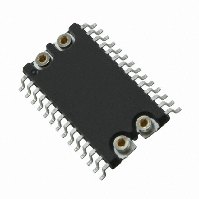
| 产品图片 |
|
| rohs | 符合RoHS无铅 / 符合限制有害物质指令(RoHS)规范要求 |
| 产品系列 | LED照明电子器件,LED照明驱动器,Texas Instruments TPS61060DRBR- |
| 数据手册 | |
| 产品型号 | TPS61060DRBR |
| 产品目录页面 | |
| 产品种类 | LED照明驱动器 |
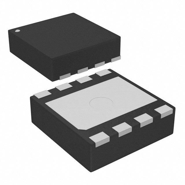
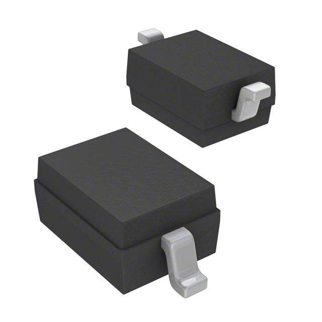
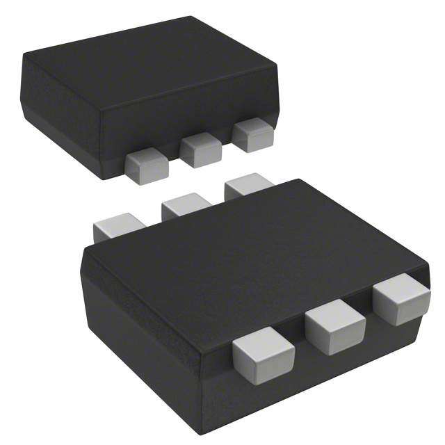
| 供应商器件封装 | 8-SON 裸露焊盘(3x3) |
| 其它名称 | 296-17500-1 |
| 内部驱动器 | 是 |
| 包装 | 剪切带 (CT) |
| 单位重量 | 24 mg |
| 商标 | Texas Instruments |
| 安装类型 | 表面贴装 |
| 安装风格 | SMD/SMT |
| 宽度 | 3 mm |
| 封装 | Reel |
| 封装/外壳 | 8-VDFN 裸露焊盘 |
| 封装/箱体 | VSON-8 |
| 工作温度 | -40°C ~ 85°C |
| 工作频率 | 1 MHz |
| 工厂包装数量 | 3000 |
| 恒压 | - |
| 恒流 | 是 |
| 拓扑 | PWM,升压(升压) |
| 拓扑结构 | Boost |
| 最大工作温度 | + 85 C |
| 最大电源电流 | 1 mA |
| 最小工作温度 | - 40 C |
| 标准包装 | 1 |
| 电压-电源 | 2.7 V ~ 6 V |
| 电压-输出 | 14.5V |
| 类型 | Inductive |
| 类型-初级 | 通用 |
| 类型-次级 | 白色 LED |
| 系列 | TPS61060 |
| 输入电压 | 2.7 V to 6 V |
| 输出数 | 1 |
| 输出电流 | 400 mA |
| 输出端数量 | 1 Output |
| 输出类型 | Constant Current |
| 频率 | 800kHz ~ 1.2MHz |
| 高电平输出电流 | 0.06 A |


- 商务部:美国ITC正式对集成电路等产品启动337调查
- 曝三星4nm工艺存在良率问题 高通将骁龙8 Gen1或转产台积电
- 太阳诱电将投资9.5亿元在常州建新厂生产MLCC 预计2023年完工
- 英特尔发布欧洲新工厂建设计划 深化IDM 2.0 战略
- 台积电先进制程称霸业界 有大客户加持明年业绩稳了
- 达到5530亿美元!SIA预计今年全球半导体销售额将创下新高
- 英特尔拟将自动驾驶子公司Mobileye上市 估值或超500亿美元
- 三星加码芯片和SET,合并消费电子和移动部门,撤换高东真等 CEO
- 三星电子宣布重大人事变动 还合并消费电子和移动部门
- 海关总署:前11个月进口集成电路产品价值2.52万亿元 增长14.8%


PDF Datasheet 数据手册内容提取
Product Sample & Technical Tools & Support & Folder Buy Documents Software Community TPS61060,TPS61061,TPS61062 SLVS538B–NOVEMBER2004–REVISEDDECEMBER2014 TPS6106x Constant Current LED Driver With Digital and PWM Brightness Control 1 Features 3 Description • LEDDriverWithIntegratedOvervoltageand The TPS6106x is a high-frequency, synchronous 1 boost converter with constant current output to drive Short-CircuitProtection up to five white LEDs. For maximum safety, the • 2.7-Vto6-VInputVoltageRange device features integrated overvoltage and an • 500-mVor250-mVFeedbackVoltage advanced short-circuit protection when the output is • TPS61060Powersupto3LEDs shorted to ground. The device operates with 1-MHz fixed switching frequency to allow for the use of small • TPS61061Powersupto4LEDs external components and to simplify possible EMI • TPS61062Powersupto5LEDs problems. The device comes with three different • PWMBrightnessControlonEnable overvoltage protection thresholds (14 V, 18 V, and 23 V) to allow inexpensive and small-output capacitors • DigitalBrightnessControlonILED with lower voltage ratings. The LED current is initially • 1-MHzFixedSwitchingFrequency set with the external sense resistor R , and the s • 400-mAInternalPowerMOSFETSwitch feedback voltage is regulated to 500 mV or 250 mV, • LEDsDisconnectedDuringShutdown depending on the configuration of the ILED pin. Digital brightness control is implemented by applying • OperatesWithSmall-OutputCapacitors a simple digital signal to the ILED pin. Alternatively, a Downto220nF PWM signal up to 1 kHz can be applied to the enable • Upto80%Efficiency pin to control the brightness of the LED. During • 8-PinNanoFree™Package(Chipscale,CSP) shutdown, the output is disconnected from the input toavoidleakagecurrentthroughtheLEDs. • 3-mm×3-mmQFNPackage DeviceInformation(1) 2 Applications PARTNUMBER PACKAGE BODYSIZE(NOM) • WhiteLEDDrivers TPS61060, VSON(8) 3.00mm×3.00mm • CellularPhones TPS61061, TPS61062 DSBGA(8) 1.446mm×1.446mm • PDAs,PocketPCs,andSmartPhones (1) For all available packages, see the orderable addendum at • DigitalStillCameras theendofthedatasheet. • HandheldDevices TypicalApplication C2 220 nF VIN L1 2.7 V to 6 V 22 (cid:2)H C1 1 (cid:2)F VIN SW EN OUT ILED FB GND PGND RS 12 (cid:1) 1 An IMPORTANT NOTICE at the end of this data sheet addresses availability, warranty, changes, use in safety-critical applications, intellectualpropertymattersandotherimportantdisclaimers.PRODUCTIONDATA.
TPS61060,TPS61061,TPS61062 SLVS538B–NOVEMBER2004–REVISEDDECEMBER2014 www.ti.com Table of Contents 1 Features.................................................................. 1 9 ApplicationandImplementation........................ 12 2 Applications........................................................... 1 9.1 ApplicationInformation............................................12 3 Description............................................................. 1 9.2 TypicalApplication..................................................12 4 RevisionHistory..................................................... 2 9.3 SystemExamples...................................................15 5 DeviceComparisonTable..................................... 3 10 PowerSupplyRecommendations..................... 17 6 PinConfigurationandFunctions......................... 3 11 Layout................................................................... 17 11.1 LayoutGuidelines.................................................17 7 Specifications......................................................... 4 11.2 LayoutExample....................................................18 7.1 AbsoluteMaximumRatings .....................................4 11.3 ThermalConsiderations........................................18 7.2 ESDRatings..............................................................4 12 DeviceandDocumentationSupport................. 19 7.3 RecommendedOperatingConditions.......................4 7.4 ThermalInformation..................................................5 12.1 DeviceSupport......................................................19 7.5 ElectricalCharacteristics...........................................5 12.2 RelatedLinks........................................................19 7.6 TypicalCharacteristics..............................................7 12.3 Trademarks...........................................................19 12.4 ElectrostaticDischargeCaution............................19 8 DetailedDescription.............................................. 9 12.5 Glossary................................................................19 8.1 Overview...................................................................9 13 Mechanical,Packaging,andOrderable 8.2 FunctionalBlockDiagram.........................................9 Information........................................................... 19 8.3 FeatureDescription...................................................9 13.1 ChipscalePackageDimensions...........................19 8.4 DeviceFunctionalModes........................................10 4 Revision History ChangesfromRevisionA(April2005)toRevisionB Page • AddedPinConfigurationandFunctionssection,ESDRatingtable,FeatureDescriptionsection,DeviceFunctional Modes,ApplicationandImplementationsection,PowerSupplyRecommendationssection,Layoutsection,Device andDocumentationSupportsection,andMechanical,Packaging,andOrderableInformationsection .............................. 1 2 SubmitDocumentationFeedback Copyright©2004–2014,TexasInstrumentsIncorporated ProductFolderLinks:TPS61060 TPS61061 TPS61062
TPS61060,TPS61061,TPS61062 www.ti.com SLVS538B–NOVEMBER2004–REVISEDDECEMBER2014 5 Device Comparison Table OVERVOLTAGE PACKAGE PACKAGEMARKING TA PROTECTION NanoFree(1) QFN(2) NanoFree QFN (OVP) 14V(min) TPS61060YZF TPS61060DRB AKX AQP –40to85°C 18V(min) TPS61061YZF TPS61061DRB AKY AQQ 22.2V(min) TPS61062YZF TPS61062DRB AKZ AQR (1) TheYZFpackageisavailableintapeandreel.AddRsuffix(TPS61060YZFR)toorderquantitiesof3000partsperreeloraddTsuffix (TPS61060YZFT)toorder250partsperreel. (2) TheDRBpackageisavailableintapeandreel.AddRsuffix(TPS61060DRBR)toorderquantitiesof3000partsperreel. 6 Pin Configuration and Functions 8-BALL 8-BALL NanoFree PACKAGE WAFER CHIP SCALE (TOP VIEW OF PCB) YZF PACKAGE Pin A1 TPS6106x DIMENSIONS Index 1 2 3 (TOP VIEW OF PCB) GND EN ILED A A1 A2 A3 B 1,50 mm VIN FB 1,424 mm B1 B3 C OUT SW PGND C1 C2 C3 1,50 mm 1,424 mm 8-Pin3x3-mmQFNPackage TopView GND 1 8 Vin EN 2 Exposed 7 OUT Thermal ILED 3 DiePad 6 SW FB 4 5 PGND PinFunctions PIN NO. I/O DESCRIPTION NAME CSP QFN VIN B1 8 I Inputsupplypinofthedevice Enablepin.Thispinneedstobepulledhightoenablethedevice.Toallowbrightnesscontrolof EN A2 2 I theLEDs,aPWMsignalupto1kHzcanbeapplied.Thispinhasaninternalpulldownresistor. GND A1 1 Analogground PGND C3 5 Powerground Thisisthefeedbackpinofthedevice.ThefeedbackpinregulatestheLEDcurrentthroughthe senseresistorbyregulatingthevoltageacrossRs.ThefeedbackvoltageissetbytheILEDpin. FB B3 4 I ILED=GNDsetsthefeedbackvoltageto500mV.ILED=highsetsthefeedbackvoltageto250 mV.Refertodigitalbrightnesscontrolsectionformoreinformation. OUT C1 7 O Outputofthedevice Copyright©2004–2014,TexasInstrumentsIncorporated SubmitDocumentationFeedback 3 ProductFolderLinks:TPS61060 TPS61061 TPS61062
TPS61060,TPS61061,TPS61062 SLVS538B–NOVEMBER2004–REVISEDDECEMBER2014 www.ti.com PinFunctions(continued) PIN NO. I/O DESCRIPTION NAME CSP QFN SW C2 6 I Switchpinofthedevice Digitalbrightnesscontrolinput.Whenthispinisgrounded,thedigitalbrightnesscontrolis disabled.Whenthispinisconnectedtohigh,thenthefeedbackvoltageisreducedtotypically ILED A3 3 I 250mVandthedigitalbrightnesscontrolisenabled.Refertodigitalbrightnesscontrolsectionfor moreinformation. ThePowerPAD™(exposedthermaldiepad)isonlyavailableontheQFNpackage.The PowerPAD™ – – PowerPAD™needstobeconnectedandsolderedtoanalogground(GND). 7 Specifications 7.1 Absolute Maximum Ratings(1) overoperatingfree-airtemperaturerange(unlessotherwisenoted) MIN MAX UNIT VIN(2) Supplyvoltagesonpin –0.3 7 V EN,ILED, Voltagesonpins –0.3 7 V FB(2) OUT(2) Voltageonpin 33 V SW(2) Voltageonpin 33 V Operatingjunctiontemperature –40 150 °C Leadtemperature(soldering,10s) 260 °C T Storagetemperature –55 150 °C stg (1) StressesbeyondthoselistedunderAbsoluteMaximumRatingsmaycausepermanentdamagetothedevice.Thesearestressratings only,andfunctionaloperationofthedeviceattheseoranyotherconditionsbeyondthoseindicatedunderRecommendedOperating Conditionsisnotimplied.Exposuretoabsolute-maximum-ratedconditionsforextendedperiodsmayaffectdevicereliability. (2) Allvoltagevaluesarewithrespecttonetworkgroundterminal. 7.2 ESD Ratings VALUE UNIT Humanbodymodel(HBM),perANSI/ESDA/JEDECJS-001(1) ±4000 V(ESD) Electrostaticdischarge Charged-devicemodel(CDM),perJEDECspecificationJESD22- ±750 V C101(2) (1) JEDECdocumentJEP155statesthat500-VHBMallowssafemanufacturingwithastandardESDcontrolprocess. (2) JEDECdocumentJEP157statesthat250-VCDMallowssafemanufacturingwithastandardESDcontrolprocess. 7.3 Recommended Operating Conditions MIN TYP MAX UNIT V Inputvoltagerange 2.7 6.0 V I L Inductor(1) 22 µH C Inputcapacitor(1) 1 µF I C Outputcapacitor(1) 0.22 1 µF O T Operatingambienttemperature -40 85 °C A T Operatingjunctiontemperature -40 125 °C J (1) Refertoapplicationsectionforfurtherinformation. 4 SubmitDocumentationFeedback Copyright©2004–2014,TexasInstrumentsIncorporated ProductFolderLinks:TPS61060 TPS61061 TPS61062
TPS61060,TPS61061,TPS61062 www.ti.com SLVS538B–NOVEMBER2004–REVISEDDECEMBER2014 7.4 Thermal Information TPS6106x THERMALMETRIC(1) DRB YZF UNIT 8PINS R Junction-to-ambientthermalresistance 47.6 120.8 θJA R Junction-to-case(top)thermalresistance 54.1 0.7 θJC(top) R Junction-to-boardthermalresistance 23.2 59.4 θJB °C/W ψ Junction-to-topcharacterizationparameter 1.0 2.2 JT ψ Junction-to-boardcharacterizationparameter 23.4 59.4 JB R Junction-to-case(bottom)thermalresistance 7.1 n/a θJC(bot) (1) Formoreinformationabouttraditionalandnewthermalmetrics,seetheICPackageThermalMetricsapplicationreport,SPRA953. 7.5 Electrical Characteristics V =3.6V,EN=V ,T =–40°Cto85°C,typicalvaluesareatT =25°C(unlessotherwisenoted) in IN A A PARAMETER TESTCONDITIONS MIN TYP MAX UNIT SUPPLYCURRENT V Inputvoltagerange 2.7 6 V IN I OperatingquiescentcurrentintoVin Devicenotswitching 1 mA Q I Shutdowncurrent EN=GND 1 10 µA SD V Undervoltagelockoutthreshold V falling 1.65 1.8 V UVLO IN V Undervoltagelockouthysteresis 50 mV HYS ENABLEANDILED V Enablehigh-levelvoltage V =2.7Vto6V 1.2 V EN IN V Enablelow-levelvoltage V =2.7Vto6V 0.4 V EN IN R Enablepulldownresistor 200 300 kΩ EN t Enable-to-shutdowndelay (1) EN=hightolow 50 ms shtdn t PWMlow-levelsignaltime (1) PWMsignalappliedtoEN 25 ms PWML V ILEDhigh-levelvoltage V =2.7Vto6V 1.2 V ILED IN V ILEDlow-levelvoltage V =2.7Vto6V 0.4 V ILED IN I ILEDinputleakagecurrent ILED=GNDorVIN 0.1 3 µA ILED DACresolution 5Bit 15.6 mV t Increasefeedbackvoltageonestep ILED=hightolow 1 75 µs up t Decreasefeedbackvoltageonestep ILED=hightolow 180 300 µs down t Delaytimebetweenup/downsteps ILED=lowtohigh 1.5 µs delay t Digitalprogrammingoff,VFB=500mV ILED=hightolow 720 µs off FEEDBACKFB I Feedbackinputbiascurrent V =500mV 1 1.5 µA FB FB V Feedbackregulationvoltage ILED=GND,afterstart-up 485 500 515 mV FB V Feedbackregulationvoltage ILED=High,afterstart-up 240 250 260 mV FB POWERSWITCHSYNCHRONOUSRECTIFIERANDCURRENTLIMIT(SW) r P-channelMOSFETon-resistance V =10V,Isw=10mA 2.5 3.7 Ω DS(ON) O N-channelMOSFETon-resistance V =V =3.6V,Isw=100mA 0.6 0.9 Ω IN GS R DS(ON) N-channelMOSFETon-resistance V =V =2.7V,Isw=100mA 0.7 1.0 Ω IN GS I Switchleakagecurrent(2) V =V =6V,V =GND, 0.1 2 µA swleak IN SW OUT EN=GND I N-ChannelMOSFETcurrentlimit V =10V 325 400 475 mA SW O (1) APWMlowsignalappliedtoENforatime(≥25ms)couldcauseadeviceshutdown.Afteraperiodof≥50msthedevicedefinitely entersshutdownmode. (2) Theswitchleakagecurrentincludestheleakagecurrentofbothinternalswitches,whichistheleakagecurrentfromSWtoground,and fromSWtoV ,withV =V . OUT IN SW Copyright©2004–2014,TexasInstrumentsIncorporated SubmitDocumentationFeedback 5 ProductFolderLinks:TPS61060 TPS61061 TPS61062
TPS61060,TPS61061,TPS61062 SLVS538B–NOVEMBER2004–REVISEDDECEMBER2014 www.ti.com Electrical Characteristics (continued) V =3.6V,EN=V ,T =–40°Cto85°C,typicalvaluesareatT =25°C(unlessotherwisenoted) in IN A A PARAMETER TESTCONDITIONS MIN TYP MAX UNIT OSCILLATOR f Switchingfrequency 0.8 1.0 1.2 MHz s OUTPUT Vovp Outputovervoltageprotection V rising;TPS61060 14 14.5 16 V O Vovp Outputovervoltageprotection V rising;TPS61061 18 18.5 19.8 V O Vovp Outputovervoltageprotection V rising;TPS61062 22.2 23.5 25 V O Vovp Outputovervoltageprotectionhysteresis TPS61060/61/62,V falling 0.7 V O Vo Outputvoltagethresholdforshort-circuit V falling V –0.7 V O IN detection Vo Outputvoltagethresholdforshort-circuit V rising V –0.3 V O IN detection Start-up,EN=lowtohigh, OUT=GND Ipre Prechargecurrentandshort-circuitcurrent VIN=6V 180 mA V =3.6V 95 IN V =2.7V 65 IN D Maximumdutycycle 95% 6 SubmitDocumentationFeedback Copyright©2004–2014,TexasInstrumentsIncorporated ProductFolderLinks:TPS61060 TPS61061 TPS61062
TPS61060,TPS61061,TPS61062 www.ti.com SLVS538B–NOVEMBER2004–REVISEDDECEMBER2014 7.6 Typical Characteristics Table1.TableofGraphs FIGURE Efficiency(η) vsLEDcurrent;2LEDs,ILED=high Figure1 vsLEDcurrent;3LEDs,ILED=low Figure2 vsLEDcurrent;3LEDs,ILED=high Figure3 vsLEDcurrent;4LEDs,ILED=low Figure4 vsLEDcurrent;4LEDs,ILED=high Figure5 vsLEDcurrent;5LEDs,ILED=high Figure6 Digitalbrightnesscontrol FeedbackvoltagevsILEDprogrammingstep Figure7 LEDcurrent vsPWMdutycycle Figure8 90 90 3IL LEEDD =S L,ow, VIN = 4.2 V 80 80 VOUT = 10.9 V VIN = 4.2 V 70 VIN = 3.6 V 70 VIN = 3.6 V Efficiency − % 5600 VIN = 3 V Efficiency − % 5600 VIN = 3 V 40 40 2 LEDS, 30 ILED = High, 30 VOUT= 7.33 V 20 20 0 10 20 30 40 50 60 0 10 20 30 40 LED Current − mA LED Current − mA Figure1.EfficiencyvsLEDCurrent Figure2.EfficiencyvsLEDCurrent 90 90 80 3IVL OLEUEDTD ==S H1,0ig.8h ,V VIN = 4.2 V 80 4IVL OLEUEDTD ==S L1,o4.w3, V VIN = 4.2 V VIN = 3.6 V − % 70 VIN = 3 V − % 70 VIN = 3.6 V VIN = 3 V cy 60 cy 60 n n e e ci ci Effi 50 Effi 50 40 40 30 30 20 20 0 10 20 30 40 0 5 10 15 20 25 30 LED Current − mA LED Current − mA Figure3.EfficiencyvsLEDCurrent Figure4.EfficiencyvsLEDCurrent Copyright©2004–2014,TexasInstrumentsIncorporated SubmitDocumentationFeedback 7 ProductFolderLinks:TPS61060 TPS61061 TPS61062
TPS61060,TPS61061,TPS61062 SLVS538B–NOVEMBER2004–REVISEDDECEMBER2014 www.ti.com 90 90 4IL LEEDD =S H,igh, VIN = 4.2 V 5IL LEEDD =S H,igh, VIN = 4.2 V 80 VOUT = 14.3 V 80 VOUT = 17.8 V 70 VIN = 3.6 V 70 VIN = 3.6 V % VIN = 3 V % Efficiency − 5600 Efficiency − 5600 VIN = 3 V 40 40 30 30 20 20 0 5 10 15 20 25 30 0 5 10 15 20 25 LED Current − mA LED Current − mA Figure5.EfficiencyvsLEDCurrent Figure6.EfficiencyvsLEDCurrent 600 22 550 Stepsize typ = 15.6 mV 20 500 mV 450 18 − ck 400 16 dba 350 mA VFB − Voltage Fee 122350500000 LED Current − 1110248 f = 1 kHz f = 500 Hz 100 50 6 0 0 1 2 3 4 5 6 7 8 9 1011121314151617 4 ILED − Programming Step f = 100 Hz 2 0 0 10 20 30 40 50 60 70 80 90 100 PWM − Duty Cycle − % Figure7.DigitalBrightnessControlFeedbackVoltagevs Figure8.LEDCurrentvsPWMDutyCycle ILEDProgrammingStep 8 SubmitDocumentationFeedback Copyright©2004–2014,TexasInstrumentsIncorporated ProductFolderLinks:TPS61060 TPS61061 TPS61062
TPS61060,TPS61061,TPS61062 www.ti.com SLVS538B–NOVEMBER2004–REVISEDDECEMBER2014 8 Detailed Description 8.1 Overview The TPS61060/61/62 family is a constant-frequency, PWM current-mode converter with an integrated N-channel MOSFET switch and synchronous P-channel MOSFET rectifier. The device operates in pulse width modulation (PWM) with a fixed switching frequency of 1 MHz. For an understanding of the device operation, refer the block diagram. The duty cycle of the converter is set by the error amplifier and the sawtooth ramp applied to the comparator. Because the control architecture is based on a current-mode control, a compensation ramp is added to allow stable operation for duty cycles larger than 50%. The converter is a fully integrated synchronous boost converter operating always in continuous conduction mode. This allows low noise operation and avoids ringing ontheswitchpinasitwouldbeseenonaconverterwhenenteringdiscontinuousconductionmode. 8.2 Functional Block Diagram SW Q2 VIN Precharge Current/PWM OUT Short-Circuit Detection T5u0r-nmoSff TBheiarsm Varle Sf =h u1t.d2o2 wVn OVP Delay UVLO Oscillator 1 MHz Vref EN Error Amplifier EN Control Logic FB Gate Drive Circuit Q1 Comparator EN EN EN S Current Limit Current Sense (cid:1) 300 k Ramp GND Compensation PGND Vref = 1.22 V ILED = High VFB = 250 mV ILED = Low VFB = 500 mV ILED Programmed VFB = 15.6 mV to 500 mV 5-Bit Digital DAC Interface ILED 15.6 mV/Step 8.3 Feature Description 8.3.1 Start-Up To avoid high inrush current during start-up, special care is taken to control the inrush current. When the device is first enabled, the output capacitor is charged with a constant precharge current of typically 100 mA until the output voltage is typically 0.3 V below VIN. The device starts with a reduced analog controlled current limit for typically 40 µs. After this time, the device enters its normal regulation with full current limit. The fixed precharge current during start-up allows the device to start up without problems when driving LEDs because the LED only starts to conduct current when the forward voltage is reached. If, for any reason a resistive load is driven, the maximumstart-uploadcurrentmustbesmaller,orequalto,theprechargecurrent. Copyright©2004–2014,TexasInstrumentsIncorporated SubmitDocumentationFeedback 9 ProductFolderLinks:TPS61060 TPS61061 TPS61062
TPS61060,TPS61061,TPS61062 SLVS538B–NOVEMBER2004–REVISEDDECEMBER2014 www.ti.com Feature Description (continued) 8.3.2 Short-CircuitProtection The TPS6106x family has an advanced short-circuit protection in case the output of the device is shorted to ground. Because the device is configured as a current source even when the LEDs are shorted, the maximum current is controlled by the sense resistor Rs. As an additional safety feature, the TPS6106x series also protects the device and inductor when the output is shorted to ground. When the output is shorted to ground, the device entersprechargemodeandlimitsthemaximumcurrenttotypically100mA. 8.3.3 OvervoltageProtection(OVP) As with any current source, the output voltage rises when the output gets high impedance or disconnected. To prevent the output voltage exceeding the maximum switch voltage rating (33 V) of the main switch, an overvoltage protection circuit is integrated. As soon as the output voltage exceeds the OVP threshold, the converter stops switching and the output voltage falls down. When the output voltage falls below the OVP threshold, the converter continues operation until the output voltage exceeds the OVP threshold again. To allow the use of inexpensive low-voltage output capacitors, the TPS6106x series has different OVP levels that must be selectedaccordingtothenumberofexternalLEDsandtheirmaximumforwardvoltage. 8.3.4 EfficiencyandFeedbackVoltage The feedback voltage has a direct effect on the converter efficiency. Because the voltage drop across the feedback resistor does not contribute to the output power (LED brightness), the lower the feedback voltage, the higher the efficiency. Especially when powering only three or less LEDs, the feedback voltage impacts the efficiency around 2% depending on the sum of the forward voltage of the LEDs. To take advantage of this, the ILEDpincanbeconnectedtoVIN,settingthefeedbackvoltageto250mV. 8.3.5 UndervoltageLockout An undervoltage lockout prevents mis-operation of the device at input voltages below typical 1.65 V. When the input voltage is below the undervoltage threshold, the device remains off and both internal MOSFETs are turned offprovidingisolationbetweeninputandoutput. 8.3.6 ThermalShutdown An internal thermal shutdown is implemented and turns off the internal MOSFETs when the typical junction temperatureof160°Cisexceeded.Thethermalshutdownhasahysteresisoftypically15°C. 8.4 Device Functional Modes 8.4.1 EnablePWMDimming The EN pin allows disabling and enabling of the device as well as brightness control of the LEDs by applying a PWM signal up to typically 1 kHz. When a PWM signal is applied, the LED current is turned on when the EN is high and off when EN is pulled low. Changing the PWM duty cycle therefore changes the LED brightness. To allow higher PWM frequencies on the enable pin, the device continues operation when a PWM signal is applied. As shown in the block diagram, the EN pin needs to be pulled low for at least 50 ms to fully turn the device off. Theenableinputpinhasaninternal300-kΩpulldownresistortodisablethedevicewhenthispinisfloating. 8.4.2 DigitalBrightnessControl(ILED) The ILED pin features a simple digital interface to allow digital brightness control. This can save processor power and battery life. Using the digital interface to control the LED brightness does not required a PWM signal all the time, and the processor can enter sleep mode if available. To save signal lines, the ILED pin can be connected totheenablepintoallowdigitalprogrammingandenable/disablefunctionatthesametimewiththesamesignal. SuchacircuitisshowninFigure9. 10 SubmitDocumentationFeedback Copyright©2004–2014,TexasInstrumentsIncorporated ProductFolderLinks:TPS61060 TPS61061 TPS61062
TPS61060,TPS61061,TPS61062 www.ti.com SLVS538B–NOVEMBER2004–REVISEDDECEMBER2014 Device Functional Modes (continued) The ILED pin basically sets the feedback regulation voltage (V ); thus, it sets the LED current. When the ILED FB pin is connected to GND, the digital brightness control is disabled and the feedback is regulated to V = FB 500 mV. When the ILED pin is pulled high, the digital brightness control is enabled starting at its midpoint where the feedback is regulated to V = 250 mV. The digital brightness control is implemented by adjusting the FB feedback voltage in digital steps with a typical maximum voltage of V = 500 mV. For this purpose, a 5-bit DAC FB is used giving 32 steps equal to a 15.6-mV change in feedback voltage per step. To increase or decrease the internal reference voltage, the ILED pin needs to be pulled low over time as outlined in Table 2 and specified in the electrical table. When the internal DAC is programmed to its highest or lowest value, it stays at this value untilitgetsprogrammedintheoppositedirectionagain. Table2.Increase/DecreaseInternalReferenceVoltage FEEDBACKVOLTAGE TIME ILEDLOGICLEVEL Increase 1µsto75µs Low Decrease 180µsto300µs Low Brightnesscontroldisabled ≥550µs Low Delaybetweensteps 1.5µs High BetweeneachcycletheILEDpinneedstobepulledhighfor1.5µs. td High ILED Low tup td tdown td toff Brightness Brightness Brightness Control Control Control Disabled Disabled Enabled Figure9. ILEDTimingDiagram Using the digital interface on the ILED pin allows simple implementation of a two-step brightness control by pulling the ILED either high or low. For full LED current with V = 500 mV, the ILED must be pulled low; to FB programhalftheLEDcurrentwithV =250mV,theILEDpinmustbepulledhigh. FB Copyright©2004–2014,TexasInstrumentsIncorporated SubmitDocumentationFeedback 11 ProductFolderLinks:TPS61060 TPS61061 TPS61062
TPS61060,TPS61061,TPS61062 SLVS538B–NOVEMBER2004–REVISEDDECEMBER2014 www.ti.com 9 Application and Implementation NOTE Information in the following applications sections is not part of the TI component specification, and TI does not warrant its accuracy or completeness. TI’s customers are responsible for determining suitability of components for their purposes. Customers should validateandtesttheirdesignimplementationtoconfirmsystemfunctionality. 9.1 Application Information The TPS6106x is designed to driver up to five LEDs in series with constant current output. The device, which operates in peak current mode PWM control, has a switch peak current limit of 325-mA minimum and internal loop compensation. The switching frequency is fixed at 1 MHz, and the input voltage range is 2.7 to 6.0 V. The following section provides a step-by-step design approach for configuring the TPS61060 to power two white LEDsinseries. 9.2 Typical Application C2 220 nF VIN L1 3 V to 6 V 22 (cid:2)H C1 1 (cid:2)F VIN SW EN OUT ILED FB GND PGND RS 12 (cid:1) Figure10. TPS61062PoweringFiveWhiteLEDs 9.2.1 DesignRequirements PARAMETER VALUE InputVoltage 3Vto6V OutputCurrent 20mA 9.2.2 DetailedDesignProcedure 9.2.2.1 InductorSelection The device requires typically a 22-µH or 10-µH inductance. When selecting the inductor, the inductor saturation current should be rated as high as the peak inductor current at maximum load, and respectively, maximum LED current. Because of the special control loop design, the inductor saturation current does not need to be rated for the maximum switch current of the converter. The maximum converter switch current usually is not reached even when the LED current is pulsed by applying a PWM signal to the enable pin. The maximum inductor peak current,aswellasLEDcurrent,iscalculatedas: Vin Dutycycle:D=1- Vout (1) Vin´D Maximum LED current:I = (lsw - )´(1-D)´h LED 2´fs´L (2) Vin´D I Inductorpeakcurrent:i = + LED Lpeak 2´fs´L (1-D)´h (3) 12 SubmitDocumentationFeedback Copyright©2004–2014,TexasInstrumentsIncorporated ProductFolderLinks:TPS61060 TPS61061 TPS61062
TPS61060,TPS61061,TPS61062 www.ti.com SLVS538B–NOVEMBER2004–REVISEDDECEMBER2014 with: fs=Switchingfrequency(1MHztypical) L=Inductorvalue η=Estimatedconverterefficiency(0.75) Isw=MinimumN-channelMOSFETcurrentlimit(325mA) (4) Using the expected converter efficiency is a simple approach to calculate maximum possible LED current as well as peak inductor current. The efficiency can be estimated by taking the efficiency numbers out of the provided efficiencycurvesortouseaworst-caseassumptionfortheexpectedefficiency,forexample,75%. 9.2.2.2 Efficiency The overall efficiency of the application depends on the specific application conditions and mainly on the selection of the inductor. A physically smaller inductor usually shows lower efficiency due to higher switching losses of the inductor (core losses, proximity losses, skin effect losses). A trade-off between physical inductor size and overall efficiency has to be made. The efficiency can typically vary around ±5% depending on the selected inductor. Figure 2 to Figure 7 can be used as a guideline for the application efficiency. These curves show the typical efficiency with a 22-µH inductor (Murata Electronics LQH32CN220K23). Figure 11 shows a basicsetupwheretheefficiencyistaken/measuredas: VLED´ILED h= Vin´Iin (5) Table3.InductorSelection INDUCTORVALUE COMPONENTSUPPLIER DIMENSIONS 10µH TDKVLF3012AT-100MR49 2.6mm×2.8mm×1.2mm 10µH MurataLQH32CN100K53 3.2mm×2.5mm×1.55mm 10µH MurataLQH32CN100K23 3.2mm×2.5mm×2.0mm 22µH TDKVLF3012AT-220MR33 2.6mm×2.8mm×1.2mm 22µH MurataLQH32CN220K53 3.2mm×2.5mm×1.55mm 22µH MurataLQH32CN220K23 3.2mm×2.5mm×2.0mm ILED C2 220 nF VIN L1 2.7 V to 6 V 22 (cid:2)H VLED Iin C1 1 (cid:2)F VIN SW Vin EN OUT ILED FB GND PGND RS 12 (cid:1) Figure11. EfficiencyMeasurementSetup Copyright©2004–2014,TexasInstrumentsIncorporated SubmitDocumentationFeedback 13 ProductFolderLinks:TPS61060 TPS61061 TPS61062
TPS61060,TPS61061,TPS61062 SLVS538B–NOVEMBER2004–REVISEDDECEMBER2014 www.ti.com 9.2.2.3 OutputCapacitorSelection The device is designed to operate with a fairly wide selection of ceramic output capacitors. The selection of the output capacitor value is a trade-off between output voltage ripple and capacitor cost and form factor. In general, capacitor values of 220 nF up to 4.7 µF can be used. When using a 220-nF output capacitor, it is recommended to use X5R or X7R dielectric material to avoid the output capacitor value falling far below 220 nF over temperature and applied voltage. For systems with wireless or RF sections, EMI is always a concern. To minimize the voltage ripple in the LED string and board traces, the output capacitor needs to be connected directly from the OUT pin of the device to ground rather than across the LEDs. A larger output capacitor value reducestheoutputvoltageripple.Table4showspossibleinputand/oroutputcapacitors. 9.2.2.4 InputCapacitorSelection Forgoodinputvoltagefiltering,lowESRceramiccapacitorsarerecommended.A1-µFceramicinputcapacitoris sufficient for most of the applications. For better input voltage filtering and EMI reduction, this value can be increased. The input capacitor should be placed as close as possible to the input pin of the converter. Table 4 showspossibleinputand/oroutputcapacitors. Table4.CapacitorSelection CAPACITOR VOLTAGERATING FORMFACTOR COMPONENTSUPPLIER(1) COMMENTS INPUTCAPACITOR 1µF 10V 0603 TayoYudenLMK107BJ105 OUTPUTCAPACITOR 220nF 16V 0603 TayoYudenEMK107BJ224 TPS61060 220nF 50V 0805 TayoYudenUMK212BJ224 TPS61060/61/62 470nF 35V 0805 TayoYudenGMK212BJ474 TPS61060/61/62 1µF 16V 0805 TayoYudenEMK212BJ105 TPS61060 1µF 35V 1206 TayoYudenGMK316BJ105 TPS61060/61/62 1µF 25V 1206 TDKC3216X7R1E105 TPS61060/61/62 (1) SimilarcapacitorsarealsoavailablefromTDKandothersuppliers. 9.2.3 ApplicationCurves C1 Frequency 199.9991 Hz EN Low Signal 2 V/div Amplitude EN 2 V/div Inductor Current LED Current 100 mA/div 20 mA/div LED Current 20 mA/div Inductor Current 1 ms/div 100 mA/div space 100 (cid:1)s/div Figure12.PWMDimming Figure13.Soft-StartOperation 14 SubmitDocumentationFeedback Copyright©2004–2014,TexasInstrumentsIncorporated ProductFolderLinks:TPS61060 TPS61061 TPS61062
TPS61060,TPS61061,TPS61062 www.ti.com SLVS538B–NOVEMBER2004–REVISEDDECEMBER2014 TPS61062 SW SW 20 V/div 20 V/div Output Voltage 20 V/div Inductor Current 200 mA/div Output Voltage 2 V/div 17 V DC Offset 20 (cid:1)s/div 500 (cid:1)s/div Figure14.Short-CircuitProtection Figure15.OvervoltageProtection SW 10 V/div Input Voltage 20 mV/div 500 ns/div Figure16.InputVoltageRipple 9.3 System Examples C2 220 nF VIN L1 2.7 V to 6 V 22 (cid:2)H C1 1 (cid:2)F VIN SW EN OUT ILED FB GND PGND RS 12 (cid:1) Figure17. TPS61060PoweringTwoWhiteLEDs Copyright©2004–2014,TexasInstrumentsIncorporated SubmitDocumentationFeedback 15 ProductFolderLinks:TPS61060 TPS61061 TPS61062
TPS61060,TPS61061,TPS61062 SLVS538B–NOVEMBER2004–REVISEDDECEMBER2014 www.ti.com System Examples (continued) C2 220 nF VIN L1 2.7 V to 6 V 22 (cid:2)H C1 1 (cid:2)F VIN SW EN OUT ILED FB GND PGND RS 12 (cid:1) Figure18. TPS61060PoweringThreeWhiteLEDs C2 220 nF VIN L1 2.7 V to 6 V 22 (cid:2)H C1 1 (cid:2)F VIN SW EN OUT ILED FB GND PGND RS 12 (cid:1) Figure19. TPS61061PoweringFourWhiteLEDs C2 220 nF VIN L1 3 V to 6 V 22 (cid:2)H C1 1 (cid:2)F VIN SW EN OUT ILED FB GND PGND RS R1 25 (cid:1) 25 (cid:1) Figure20. TPS61060PoweringSixWhiteLEDs 16 SubmitDocumentationFeedback Copyright©2004–2014,TexasInstrumentsIncorporated ProductFolderLinks:TPS61060 TPS61061 TPS61062
TPS61060,TPS61061,TPS61062 www.ti.com SLVS538B–NOVEMBER2004–REVISEDDECEMBER2014 System Examples (continued) C2 220 nF VIN L1 2.7 V to 6 V 22 (cid:3)H C1 1 (cid:3)F VIN SW EN OUT Digital ILED FB Brightness Control GND PGND RS 12 (cid:2) Thiscircuitcombinestheenablewiththedigitalbrightnesscontrolpin,allowingthedigitalsignalappliedtoILEDto alsoenableanddisablethedevice. Figure21. TPS61061DigitalBrightnessControl 10 Power Supply Recommendations The TPS6106x is designed to operate from an input voltage supply range from 2.7-V to 6.0-V. The power supply to the TPS6106x must have a current rating according to the supply voltage, output voltage, and output current oftheTPS6106xdevice. 11 Layout 11.1 Layout Guidelines As for all switching power supplies, the layout is an important step in the design, especially at high peak currents and switching frequencies. If the layout is not carefully done, the regulator might show noise problems and duty cycle jitter. The input capacitor should be placed as close as possible to the input pin for good input voltage filtering. The inductor should be placed as close as possible to the switch pin to minimize the noise coupling into other circuits. The output capacitor needs to be placed directly from the OUT pin to GND rather than across the LEDs. This reduces the ripple current in the trace to the LEDs. The GND pin must be connected directly to the PGND pin. When doing the PCB layout, the bold traces (Figure 22) should be routed first, as well as placement oftheinductor,andinputandoutputcapacitors. Copyright©2004–2014,TexasInstrumentsIncorporated SubmitDocumentationFeedback 17 ProductFolderLinks:TPS61060 TPS61061 TPS61062
TPS61060,TPS61061,TPS61062 SLVS538B–NOVEMBER2004–REVISEDDECEMBER2014 www.ti.com 11.2 Layout Example GND VIN GND 1 8 VIN T P EN 2 S 7 OUT LED+ 6 ILED 3 1 6 SW 0 6 FB 4 x 5 PGND LED- Figure22. TPS6106xLayoutExample 11.3 Thermal Considerations The TPS6106x comes in a thermally enhanced QFN package. The package includes a thermal pad that improves the thermal capabilities of the package. Also see QFN/SON PCB Attachment application report (SLUA271). The thermal resistance junction-to-ambient R of the QFN package greatly depends on the PCB θJA layout. Using thermal vias and wide PCB traces improves the thermal resistance R . The thermal pad must be θJA solderedtotheanaloggroundonthePCB. For the NanoFree package, similar guidelines apply for the QFN package. The thermal resistance R depends θJA mainlyonthePCBlayout. 18 SubmitDocumentationFeedback Copyright©2004–2014,TexasInstrumentsIncorporated ProductFolderLinks:TPS61060 TPS61061 TPS61062
TPS61060,TPS61061,TPS61062 www.ti.com SLVS538B–NOVEMBER2004–REVISEDDECEMBER2014 12 Device and Documentation Support 12.1 Device Support 12.1.1 Third-PartyProductsDisclaimer TI'S PUBLICATION OF INFORMATION REGARDING THIRD-PARTY PRODUCTS OR SERVICES DOES NOT CONSTITUTE AN ENDORSEMENT REGARDING THE SUITABILITY OF SUCH PRODUCTS OR SERVICES OR A WARRANTY, REPRESENTATION OR ENDORSEMENT OF SUCH PRODUCTS OR SERVICES, EITHER ALONEORINCOMBINATIONWITHANYTIPRODUCTORSERVICE. 12.2 Related Links The table below lists quick access links. Categories include technical documents, support and community resources,toolsandsoftware,andquickaccesstosampleorbuy. Table5.RelatedLinks TECHNICAL TOOLS& SUPPORT& PARTS PRODUCTFOLDER SAMPLE&BUY DOCUMENTS SOFTWARE COMMUNITY TPS61060 Clickhere Clickhere Clickhere Clickhere Clickhere TPS61061 Clickhere Clickhere Clickhere Clickhere Clickhere TPS61062 Clickhere Clickhere Clickhere Clickhere Clickhere 12.3 Trademarks NanoFree,PowerPADaretrademarksofTexasInstruments. Allothertrademarksarethepropertyoftheirrespectiveowners. 12.4 Electrostatic Discharge Caution Thesedeviceshavelimitedbuilt-inESDprotection.Theleadsshouldbeshortedtogetherorthedeviceplacedinconductivefoam duringstorageorhandlingtopreventelectrostaticdamagetotheMOSgates. 12.5 Glossary SLYZ022—TIGlossary. Thisglossarylistsandexplainsterms,acronyms,anddefinitions. 13 Mechanical, Packaging, and Orderable Information The following pages include mechanical, packaging, and orderable information. This information is the most current data available for the designated devices. This data is subject to change without notice and revision of thisdocument.Forbrowser-basedversionsofthisdatasheet,refertotheleft-handnavigation. 13.1 Chipscale Package Dimensions The TPS6106x is available in a Chipscale package and has the following mechanical dimensions: E=D=1,446 mm (typical), E=D=1,424 mm (minimum), E=D=1,5 mm (maximum). See the mechanical drawing of the package (YZF). Copyright©2004–2014,TexasInstrumentsIncorporated SubmitDocumentationFeedback 19 ProductFolderLinks:TPS61060 TPS61061 TPS61062
PACKAGE OPTION ADDENDUM www.ti.com 6-Feb-2020 PACKAGING INFORMATION Orderable Device Status Package Type Package Pins Package Eco Plan Lead/Ball Finish MSL Peak Temp Op Temp (°C) Device Marking Samples (1) Drawing Qty (2) (6) (3) (4/5) TPS61060DRBR ACTIVE SON DRB 8 3000 Green (RoHS NIPDAU Level-2-260C-1 YEAR -40 to 85 AQP & no Sb/Br) TPS61060DRBRG4 ACTIVE SON DRB 8 3000 Green (RoHS NIPDAU Level-2-260C-1 YEAR -40 to 85 AQP & no Sb/Br) TPS61060YZFR ACTIVE DSBGA YZF 8 3000 Green (RoHS SNAGCU Level-1-260C-UNLIM -40 to 85 AKX & no Sb/Br) TPS61060YZFT ACTIVE DSBGA YZF 8 250 Green (RoHS SNAGCU Level-1-260C-UNLIM -40 to 85 AKX & no Sb/Br) TPS61061DRBR ACTIVE SON DRB 8 3000 Green (RoHS NIPDAU Level-2-260C-1 YEAR -40 to 85 AQQ & no Sb/Br) TPS61061DRBRG4 ACTIVE SON DRB 8 3000 Green (RoHS NIPDAU Level-2-260C-1 YEAR -40 to 85 AQQ & no Sb/Br) TPS61061YZFT ACTIVE DSBGA YZF 8 250 Green (RoHS SNAGCU Level-1-260C-UNLIM -40 to 85 AKY & no Sb/Br) TPS61062DRBR ACTIVE SON DRB 8 3000 Green (RoHS NIPDAU Level-2-260C-1 YEAR -40 to 85 AQR & no Sb/Br) TPS61062YZFR ACTIVE DSBGA YZF 8 3000 Green (RoHS SNAGCU Level-1-260C-UNLIM -40 to 85 AKZ & no Sb/Br) TPS61062YZFT ACTIVE DSBGA YZF 8 250 Green (RoHS SNAGCU Level-1-260C-UNLIM -40 to 85 AKZ & no Sb/Br) (1) The marketing status values are defined as follows: ACTIVE: Product device recommended for new designs. LIFEBUY: TI has announced that the device will be discontinued, and a lifetime-buy period is in effect. NRND: Not recommended for new designs. Device is in production to support existing customers, but TI does not recommend using this part in a new design. PREVIEW: Device has been announced but is not in production. Samples may or may not be available. OBSOLETE: TI has discontinued the production of the device. (2) RoHS: TI defines "RoHS" to mean semiconductor products that are compliant with the current EU RoHS requirements for all 10 RoHS substances, including the requirement that RoHS substance do not exceed 0.1% by weight in homogeneous materials. Where designed to be soldered at high temperatures, "RoHS" products are suitable for use in specified lead-free processes. TI may reference these types of products as "Pb-Free". RoHS Exempt: TI defines "RoHS Exempt" to mean products that contain lead but are compliant with EU RoHS pursuant to a specific EU RoHS exemption. Green: TI defines "Green" to mean the content of Chlorine (Cl) and Bromine (Br) based flame retardants meet JS709B low halogen requirements of <=1000ppm threshold. Antimony trioxide based flame retardants must also meet the <=1000ppm threshold requirement. (3) MSL, Peak Temp. - The Moisture Sensitivity Level rating according to the JEDEC industry standard classifications, and peak solder temperature. Addendum-Page 1
PACKAGE OPTION ADDENDUM www.ti.com 6-Feb-2020 (4) There may be additional marking, which relates to the logo, the lot trace code information, or the environmental category on the device. (5) Multiple Device Markings will be inside parentheses. Only one Device Marking contained in parentheses and separated by a "~" will appear on a device. If a line is indented then it is a continuation of the previous line and the two combined represent the entire Device Marking for that device. (6) Lead/Ball Finish - Orderable Devices may have multiple material finish options. Finish options are separated by a vertical ruled line. Lead/Ball Finish values may wrap to two lines if the finish value exceeds the maximum column width. Important Information and Disclaimer:The information provided on this page represents TI's knowledge and belief as of the date that it is provided. TI bases its knowledge and belief on information provided by third parties, and makes no representation or warranty as to the accuracy of such information. Efforts are underway to better integrate information from third parties. TI has taken and continues to take reasonable steps to provide representative and accurate information but may not have conducted destructive testing or chemical analysis on incoming materials and chemicals. TI and TI suppliers consider certain information to be proprietary, and thus CAS numbers and other limited information may not be available for release. In no event shall TI's liability arising out of such information exceed the total purchase price of the TI part(s) at issue in this document sold by TI to Customer on an annual basis. Addendum-Page 2
PACKAGE MATERIALS INFORMATION www.ti.com 1-Jan-2020 TAPE AND REEL INFORMATION *Alldimensionsarenominal Device Package Package Pins SPQ Reel Reel A0 B0 K0 P1 W Pin1 Type Drawing Diameter Width (mm) (mm) (mm) (mm) (mm) Quadrant (mm) W1(mm) TPS61060DRBR SON DRB 8 3000 330.0 12.4 3.3 3.3 1.1 8.0 12.0 Q2 TPS61060YZFR DSBGA YZF 8 3000 180.0 8.4 1.65 1.65 0.81 4.0 8.0 Q1 TPS61060YZFT DSBGA YZF 8 250 180.0 8.4 1.65 1.65 0.81 4.0 8.0 Q1 TPS61061DRBR SON DRB 8 3000 330.0 12.4 3.3 3.3 1.1 8.0 12.0 Q2 TPS61062DRBR SON DRB 8 3000 330.0 12.4 3.3 3.3 1.1 8.0 12.0 Q2 TPS61062YZFR DSBGA YZF 8 3000 180.0 8.4 1.65 1.65 0.81 4.0 8.0 Q1 TPS61062YZFT DSBGA YZF 8 250 180.0 8.4 1.65 1.65 0.81 4.0 8.0 Q1 PackMaterials-Page1
PACKAGE MATERIALS INFORMATION www.ti.com 1-Jan-2020 *Alldimensionsarenominal Device PackageType PackageDrawing Pins SPQ Length(mm) Width(mm) Height(mm) TPS61060DRBR SON DRB 8 3000 367.0 367.0 35.0 TPS61060YZFR DSBGA YZF 8 3000 182.0 182.0 20.0 TPS61060YZFT DSBGA YZF 8 250 182.0 182.0 20.0 TPS61061DRBR SON DRB 8 3000 367.0 367.0 35.0 TPS61062DRBR SON DRB 8 3000 367.0 367.0 35.0 TPS61062YZFR DSBGA YZF 8 3000 182.0 182.0 20.0 TPS61062YZFT DSBGA YZF 8 250 182.0 182.0 20.0 PackMaterials-Page2
None
PACKAGE OUTLINE DRB0008A VSON - 1 mm max height SCALE 4.000 PLASTIC SMALL OUTLINE - NO LEAD 3.1 B A 2.9 PIN 1 INDEX AREA 3.1 2.9 C 1 MAX SEATING PLANE 0.05 0.08 C DIM A 0.00 OPT 1 OPT 2 1.5 0.1 (0.1) (0.2) 4X (0.23) EXPOSED (DIM A) TYP THERMAL PAD 4 5 2X 1.95 1.75 0.1 8 1 6X 0.65 0.37 8X 0.25 PIN 1 ID 0.1 C A B (OPTIONAL) (0.65) 0.05 C 0.5 8X 0.3 4218875/A 01/2018 NOTES: 1. All linear dimensions are in millimeters. Any dimensions in parenthesis are for reference only. Dimensioning and tolerancing per ASME Y14.5M. 2. This drawing is subject to change without notice. 3. The package thermal pad must be soldered to the printed circuit board for thermal and mechanical performance. www.ti.com
EXAMPLE BOARD LAYOUT DRB0008A VSON - 1 mm max height PLASTIC SMALL OUTLINE - NO LEAD (1.5) (0.65) SYMM 8X (0.6) (0.825) 8X (0.31) 1 8 SYMM (1.75) (0.625) 6X (0.65) 4 5 (R0.05) TYP ( 0.2) VIA TYP (0.23) (0.5) (2.8) LAND PATTERN EXAMPLE EXPOSED METAL SHOWN SCALE:20X 0.07 MAX 0.07 MIN ALL AROUND ALL AROUND EXPOSED EXPOSED METAL METAL SOLDER MASK METAL METAL UNDER SOLDER MASK OPENING SOLDER MASK OPENING NON SOLDER MASK SOLDER MASK DEFINED DEFINED (PREFERRED) SOLDER MASK DETAILS 4218875/A 01/2018 NOTES: (continued) 4. This package is designed to be soldered to a thermal pad on the board. For more information, see Texas Instruments literature number SLUA271 (www.ti.com/lit/slua271). 5. Vias are optional depending on application, refer to device data sheet. If any vias are implemented, refer to their locations shown on this view. It is recommended that vias under paste be filled, plugged or tented. www.ti.com
EXAMPLE STENCIL DESIGN DRB0008A VSON - 1 mm max height PLASTIC SMALL OUTLINE - NO LEAD (0.65) 4X (0.23) SYMM METAL TYP 8X (0.6) 4X (0.725) 8X (0.31) 1 8 (2.674) SYMM (1.55) 6X (0.65) 4 5 (R0.05) TYP (1.34) (2.8) SOLDER PASTE EXAMPLE BASED ON 0.125 mm THICK STENCIL EXPOSED PAD 84% PRINTED SOLDER COVERAGE BY AREA SCALE:25X 4218875/A 01/2018 NOTES: (continued) 6. Laser cutting apertures with trapezoidal walls and rounded corners may offer better paste release. IPC-7525 may have alternate design recommendations. www.ti.com
D: Max = 1.49 mm, Min = 1.43 mm E: Max = 1.49 mm, Min = 1.43 mm
IMPORTANTNOTICEANDDISCLAIMER TI PROVIDES TECHNICAL AND RELIABILITY DATA (INCLUDING DATASHEETS), DESIGN RESOURCES (INCLUDING REFERENCE DESIGNS), APPLICATION OR OTHER DESIGN ADVICE, WEB TOOLS, SAFETY INFORMATION, AND OTHER RESOURCES “AS IS” AND WITH ALL FAULTS, AND DISCLAIMS ALL WARRANTIES, EXPRESS AND IMPLIED, INCLUDING WITHOUT LIMITATION ANY IMPLIED WARRANTIES OF MERCHANTABILITY, FITNESS FOR A PARTICULAR PURPOSE OR NON-INFRINGEMENT OF THIRD PARTY INTELLECTUAL PROPERTY RIGHTS. These resources are intended for skilled developers designing with TI products. You are solely responsible for (1) selecting the appropriate TI products for your application, (2) designing, validating and testing your application, and (3) ensuring your application meets applicable standards, and any other safety, security, or other requirements. These resources are subject to change without notice. TI grants you permission to use these resources only for development of an application that uses the TI products described in the resource. Other reproduction and display of these resources is prohibited. No license is granted to any other TI intellectual property right or to any third party intellectual property right. TI disclaims responsibility for, and you will fully indemnify TI and its representatives against, any claims, damages, costs, losses, and liabilities arising out of your use of these resources. TI’s products are provided subject to TI’s Terms of Sale (www.ti.com/legal/termsofsale.html) or other applicable terms available either on ti.com or provided in conjunction with such TI products. TI’s provision of these resources does not expand or otherwise alter TI’s applicable warranties or warranty disclaimers for TI products. Mailing Address: Texas Instruments, Post Office Box 655303, Dallas, Texas 75265 Copyright © 2020, Texas Instruments Incorporated