ICGOO在线商城 > 集成电路(IC) > PMIC - 稳压器 - DC DC 开关稳压器 > TPS60151DRVT
 Datasheet下载
- 型号: TPS60151DRVT
- 制造商: Texas Instruments
- 库位|库存: xxxx|xxxx
- 要求:
| 数量阶梯 | 香港交货 | 国内含税 |
| +xxxx | $xxxx | ¥xxxx |
查看当月历史价格
查看今年历史价格
TPS60151DRVT产品简介:
ICGOO电子元器件商城为您提供TPS60151DRVT由Texas Instruments设计生产,在icgoo商城现货销售,并且可以通过原厂、代理商等渠道进行代购。 TPS60151DRVT价格参考。Texas InstrumentsTPS60151DRVT封装/规格:PMIC - 稳压器 - DC DC 开关稳压器, 固定 充电泵 开关稳压器 IC 正 5V 1 输出 140mA 6-WDFN 裸露焊盘。您可以下载TPS60151DRVT参考资料、Datasheet数据手册功能说明书,资料中有TPS60151DRVT 详细功能的应用电路图电压和使用方法及教程。
TPS60151DRVT 是 Texas Instruments(德州仪器)生产的一款 DC-DC 开关稳压器,属于 PMIC(电源管理集成电路)类别。该器件主要用作升压(Boost)转换器,能够将较低的输入电压升高至较高的稳定输出电压,具有高效率、小尺寸和高集成度的特点。

 主要应用场景包括:

1. 便携式电子设备:如智能手机、平板电脑、移动电源等,用于电池供电系统中,将电池电压升压至系统所需电压,为显示屏、传感器、无线模块等供电。

2. 工业控制系统:在工业自动化设备中,为传感器、执行器、PLC(可编程逻辑控制器)等提供稳定电源。

3. LED 照明:用于驱动高亮度 LED 灯串,提供恒定电流或电压,适用于背光显示、照明设备等。

4. 无线通信模块:如 Wi-Fi、蓝牙、LoRa 等模块的电源管理,确保模块在不同工作状态下的稳定供电。

5. 汽车电子系统:用于车载设备中,如仪表盘、导航系统、行车记录仪等,适应车辆电压波动环境,提供稳定输出。

该器件采用小型封装(如 10-SON),适合对空间要求严格的高密度电路设计,且具备软启动、过流保护等功能,提升系统稳定性与可靠性。
| 参数 | 数值 |
| 产品目录 | 集成电路 (IC)半导体 |
| 描述 | IC REG BOOST SWITCHD CAP 5V 6SON稳压器—开关式稳压器 140mA,5V Charge Pump |
| DevelopmentKit | TPS60151EVM-359 |
| 产品分类 | |
| 品牌 | Texas Instruments |
| 产品手册 | |
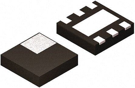
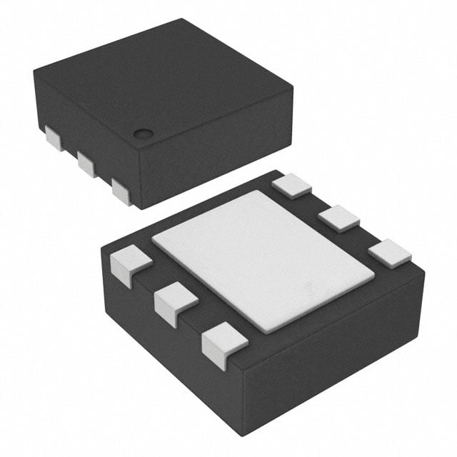
| 产品图片 |
|
| rohs | 符合RoHS无铅 / 符合限制有害物质指令(RoHS)规范要求 |
| 产品系列 | 电源管理 IC,稳压器—开关式稳压器,Texas Instruments TPS60151DRVT- |
| 数据手册 | |
| 产品型号 | TPS60151DRVT |
| PWM类型 | - |
| 产品种类 | 稳压器—开关式稳压器 |
| 供应商器件封装 | 6-SON(2x2) |
| 其它名称 | 296-32495-1 |
| 包装 | 剪切带 (CT) |
| 同步整流器 | 无 |
| 商标 | Texas Instruments |
| 安装类型 | 表面贴装 |
| 安装风格 | SMD/SMT |
| 封装 | Reel |
| 封装/外壳 | 6-WDFN 裸露焊盘 |
| 封装/箱体 | WSON-6 |
| 工作温度 | -40°C ~ 85°C |
| 工作温度范围 | - 40 C to + 85 C |
| 工厂包装数量 | 250 |
| 开关频率 | 1.5 MHz |
| 拓扑结构 | Boost |
| 最大工作温度 | + 85 C |
| 最大输入电压 | 5.5 V |
| 最小工作温度 | - 40 C |
| 标准包装 | 1 |
| 电压-输入 | 2.7 V ~ 5.5 V |
| 电压-输出 | 5V |
| 电流-输出 | 140mA |
| 类型 | 升压(升压),切换电容(充电泵) |
| 系列 | TPS60151 |
| 输出数 | 1 |
| 输出电压 | 5 V |
| 输出电流 | 140 mA |
| 输出端数量 | 1 Output |
| 输出类型 | 固定 |
| 配用 | /product-detail/zh/TPS60151EVM-359/296-31213-ND/2262034 |
| 频率-开关 | 1.5MHz |


- 商务部:美国ITC正式对集成电路等产品启动337调查
- 曝三星4nm工艺存在良率问题 高通将骁龙8 Gen1或转产台积电
- 太阳诱电将投资9.5亿元在常州建新厂生产MLCC 预计2023年完工
- 英特尔发布欧洲新工厂建设计划 深化IDM 2.0 战略
- 台积电先进制程称霸业界 有大客户加持明年业绩稳了
- 达到5530亿美元!SIA预计今年全球半导体销售额将创下新高
- 英特尔拟将自动驾驶子公司Mobileye上市 估值或超500亿美元
- 三星加码芯片和SET,合并消费电子和移动部门,撤换高东真等 CEO
- 三星电子宣布重大人事变动 还合并消费电子和移动部门
- 海关总署:前11个月进口集成电路产品价值2.52万亿元 增长14.8%


PDF Datasheet 数据手册内容提取
Product Order Technical Tools & Support & Folder Now Documents Software Community TPS60151 SLVSA02B–SEPTEMBER2009–REVISEDJANUARY2019 TPS60151 5-V and 140-mA Charge Pump 1 Features 3 Description • InputVoltageRange2.7Vto5.5V The TPS60151 is a switched capacitor voltage 1 converter which produces a regulated, low noise, and • FixedOutputVoltageof5V low-ripple output voltage of 5 V from an unregulated • MaximumOutputCurrent:140mA input voltage. It maintains 5-V regulation even when • 1.5-MHzSwitchingFrequency VIN isgreaterthan5V. • Typical90-μAQuiescentCurrentatNoLoad The 5-V output can supply a minimum of 140-mA Condition(SkipMode) current. • OutputReverseCurrentProtection The TPS60151 has built-in current limit and output • X2ChargePump reverse current protection that are ideal for HDMI, USBOTGandotherbatterypoweredapplications. • HardwareEnableandDisableFunction • Built-inSoftStart TPS60151 operates in skip mode when the load current falls below 8 mA under typical condition. In • Built-inUndervoltageLockoutProtection skip mode operation, quiescent current is reduced to • ThermalandOvercurrentProtection 90μA. • 2-mm×2-mm6-PinSON-Packagewith0.8-mm Only 3 external capacitors are needed to generate Height theoutputvoltage,therebysavingPCBspace. 2 Applications Inrush current is limited by the soft-start function duringpoweronandpowertransientstates. • USBOntheGo(OTG) The TPS60151 operates over a free air temperature • HDMI range of –40°C to 85°C. The device is available with • PortableCommunicationDevices asmall2-mm×2-mm6-pinSONpackage(QFN). • PCMCIACards • MobilePhones,SmartPhones DeviceInformation(1) • HandheldMeters PARTNUMBER PACKAGE BODYSIZE(NOM) TPS60151 WSON(6) 2.00mm×2.00mm (1) For all available packages, see the orderable addendum at theendofthedatasheet. TypicalApplicationSchematic EfficiencyvsInputVoltage ENABLE 100 GND ENA /DISABLE 90 TA= 25°C VIN VIN CP- 150 mA C2 VOUT 2.2μF 80 VOUT CP+ 120 mA (5.0V) 50 mA 70 C3 C1 100 mA 2.2μF 4.7μF y - % 60 10 mA c n 50 e ci Effi 40 30 20 10 0 2.7 3.2 3.7 4.2 4.7 5.2 V - Input Voltage - V I 1 An IMPORTANT NOTICE at the end of this data sheet addresses availability, warranty, changes, use in safety-critical applications, intellectualpropertymattersandotherimportantdisclaimers.PRODUCTIONDATA.
TPS60151 SLVSA02B–SEPTEMBER2009–REVISEDJANUARY2019 www.ti.com Table of Contents 1 Features.................................................................. 1 8.4 DeviceFunctionalModes..........................................9 2 Applications........................................................... 1 9 ApplicationandImplementation........................ 12 3 Description............................................................. 1 9.1 ApplicationInformation............................................12 4 RevisionHistory..................................................... 2 9.2 TypicalApplication .................................................12 9.3 SystemExample.....................................................16 5 DeviceComparisonTable..................................... 3 10 PowerSupplyRecommendations..................... 17 6 PinConfigurationandFunctions......................... 3 11 Layout................................................................... 17 7 Specifications......................................................... 4 11.1 LayoutGuidelines.................................................17 7.1 AbsoluteMaximumRatings......................................4 11.2 LayoutExample....................................................17 7.2 ESDRatings..............................................................4 12 DeviceandDocumentationSupport................. 18 7.3 RecommendedOperatingConditions.......................4 7.4 ThermalInformation..................................................4 12.1 ReceivingNotificationofDocumentationUpdates18 7.5 ElectricalCharacteristics...........................................5 12.2 CommunityResources..........................................18 7.6 TypicalCharacteristics..............................................6 12.3 Trademarks...........................................................18 12.4 ElectrostaticDischargeCaution............................18 8 DetailedDescription.............................................. 7 12.5 Glossary................................................................18 8.1 Overview...................................................................7 13 Mechanical,Packaging,andOrderable 8.2 FunctionalBlockDiagram.........................................8 Information........................................................... 18 8.3 FeatureDescription...................................................8 4 Revision History NOTE:Pagenumbersforpreviousrevisionsmaydifferfrompagenumbersinthecurrentversion. ChangesfromRevisionA(October2015)toRevisionB Page • AddedrowforV spec--3.1V≤V <5.5V...................................................................................................................... 5 OUT IN • AddedrowforV Vspec--3.1V≤V <5.5V............................................................................................................. 5 OUT(skip) IN ChangesfromOriginal(August2009)toRevisionA Page • AddedPinConfigurationandFunctionssection,ESDRatingstable,FeatureDescriptionsection,DeviceFunctional Modes,ApplicationandImplementationsection,PowerSupplyRecommendationssection,Layoutsection,Device andDocumentationSupportsection,andMechanical,Packaging,andOrderableInformationsection .............................. 1 2 SubmitDocumentationFeedback Copyright©2009–2019,TexasInstrumentsIncorporated ProductFolderLinks:TPS60151
TPS60151 www.ti.com SLVSA02B–SEPTEMBER2009–REVISEDJANUARY2019 5 Device Comparison Table PARTNUMBER (1) OUTPUTVOLTAGE PACKAGE ORDERING PACKAGEMARKING DESIGNATOR TPS60151 5V DRV TPS60151DRV OCN (1) TheDRV(2mm×2mm6-pinSON)packageisavailableintapeonreel.AddRsuffixtoorderquantitiesof3000partsperreelandT suffixtoorderquantitieswith250partsperreel. 6 Pin Configuration and Functions QFNPackage 6-PinWSON TopView GND ENA VIN CP- VOUT CP+ PinFunctions PIN I/O DESCRIPTION NAME NO. GND 1 – Ground VIN 2 IN Supplyvoltageinput VOUT 3 OUT Output,connecttotheoutputcapacitor CP+ 4 – Connecttotheflyingcapacitor CP– 5 – Connecttotheflyingcapacitor ENA 6 IN Hardwareenable/disablepin(High=Enable) Copyright©2009–2019,TexasInstrumentsIncorporated SubmitDocumentationFeedback 3 ProductFolderLinks:TPS60151
TPS60151 SLVSA02B–SEPTEMBER2009–REVISEDJANUARY2019 www.ti.com 7 Specifications 7.1 Absolute Maximum Ratings Overoperatingfree-airtemperaturerange(unlessotherwisenoted) (1) MIN MAX UNIT V Inputvoltage(allpins) –0.3 7 V IN T Operatingtemperature –40 85 °C A T Maximumoperatingjunctiontemperature 150 °C J T Storagetemperature –55 150 °C stg (1) StressesbeyondthoselistedunderAbsoluteMaximumRatingsmaycausepermanentdamagetothedevice.Thesearestressratings onlyandfunctionaloperationofthedeviceattheseoranyotherconditionsbeyondthoseindicatedunderRecommendedOperating Conditionsisnotimplied.Exposuretoabsolute-maximum-ratedconditionsforextendedperiodsmayaffectdevicereliability. 7.2 ESD Ratings VALUE UNIT Humanbodymodel(HBM),perANSI/ESDA/JEDECJS-001(1)(2) ±2000 V(ESD) Electrostaticdischarge Charged-devicemodel(CDM),perJEDECspecificationJESD22- ±500 V C101(3) (1) JEDECdocumentJEP155statesthat500-VHBMallowssafemanufacturingwithastandardESDcontrolprocess. (2) TheHumanbodymodel(HBM)isa100pFcapacitordischargedthrougha1.5kΩresistorintoeachpin.Thetestingisdoneaccording JEDECsEIA/JESD22-A114. (3) JEDECdocumentJEP157statesthat250-VCDMallowssafemanufacturingwithastandardESDcontrolprocess. 7.3 Recommended Operating Conditions overoperatingfree-airtemperaturerange(unlessotherwisenoted) MIN NOM MAX UNIT V Inputvoltage 2.7 5.5 V IN T Operatingambienttemperature –40 85 °C A T Operatingjunctiontemperature –40 125 °C J C Inputcapacitor 2.2 μF IN C Outputcapacitor 2.2 μF OUT C Flyingcapacitor 1.0 μF F 7.4 Thermal Information TPS60151 THERMALMETRIC(1) DRV(WSON) UNIT 6PINS R Junction-to-ambientthermalresistance 69.1 °C/W θJA R Junction-to-case(top)thermalresistance 79.8 °C/W θJC(top) R Junction-to-boardthermalresistance 38.6 °C/W θJB ψ Junction-to-topcharacterizationparameter 1.2 °C/W JT ψ Junction-to-boardcharacterizationparameter 38.4 °C/W JB R Junction-to-case(bottom)thermalresistance 9.2 °C/W θJC(bot) (1) Formoreinformationabouttraditionalandnewthermalmetrics,seetheSemiconductorandICPackageThermalMetricsapplication report,SPRA953. 4 SubmitDocumentationFeedback Copyright©2009–2019,TexasInstrumentsIncorporated ProductFolderLinks:TPS60151
TPS60151 www.ti.com SLVSA02B–SEPTEMBER2009–REVISEDJANUARY2019 7.5 Electrical Characteristics V =3.6V,T =–40°Cto+85°C,typicalvaluesareatT =25°C,C1=C3=2.2μF,C2=1μF(unlessotherwisenoted) IN A A PARAMETER TESTCONDITIONS MIN TYP MAX UNIT POWERSTAGE V Inputvoltagerange 2.7 5.5 V IN V Undervoltagelockoutthreshold 1.9 2.1 V UVLO I Operatingquiescentcurrent I =140mA,Enable=V 4.7 mA Q OUT IN I Skipmodeoperatingquiescent I =0mA,Enable=V (noswitching) 80 μA Qskip OUT IN current I =0mA,Enable=V (minimum 90 μA OUT IN switching) I Shutdowncurrent 2.7V≤V ≤5.5V,Enable=0V 4 10 μA SD IN V Outputvoltage(1) I ≤50mA,2.7V≤V <5.5V 4.8 5 5.2 V OUT OUT IN I ≤50mA,3.1V≤V <5.5V 4.8 5 5.15 V OUT IN V V Skipmodeoutputvoltage I =0mA,2.7V≤V ≤5.5V V +0.1 V OUT(skip) OUT IN OUT I =0mA,3.1V≤V ≤5.5V V +0.1 5.25 V OUT IN OUT F Switchingfrequency 1.5 MHz SW t Soft-starttime Fromtherisingedgeofenableto90%output 150 μs SS OUTPUTCURRENT I Maximumoutputcurrent V remainsbetween4.8Vand5.2V, 120 mA OUT_nom OUT 3.1V≤V ≤5.5V IN 3.3V<V <5.5V 140 IN I Currentlimit V =4.5V 500 mA OUT_max OUT I Shortcircuitcurrent(2) V =0V 80 mA OUT_short OUT RIPPLEVOLTAGE V Outputripplevoltage I =140mA 30 mV R OUT ENABLECONTROL V Logichighinputvoltage 2.7V≤V ≤5.5V 1.3 V V HI IN IN V Logiclowinputvoltage –0.2 0.4 V LI I Logichighinputcurrent 1 μA HI I Logiclowinputcurrent 1 μA LI THERMALSHUTDOWN T Shutdowntemperature 160 °C SD T Shutdownrecovery 140 °C RC (1) Wheninskipmode,outputvoltagecanexceedV specbecauseV =V +0.1. OUT OUT(skip) OUT (2) TPS60151hasinternalprotectioncircuittoprotectICwhenV shortedtoGND. OUT Copyright©2009–2019,TexasInstrumentsIncorporated SubmitDocumentationFeedback 5 ProductFolderLinks:TPS60151
TPS60151 SLVSA02B–SEPTEMBER2009–REVISEDJANUARY2019 www.ti.com 7.6 Typical Characteristics 120 0.3 TA= -40°C No load 110 No Switching 0.25 A Input Current -Aµ1089000 -85°C Max Output Current - 0.001..152 TA= 25°C TA= 85°C 25°C -40°C - O I 70 0.05 60 0 2.7 3.2 3.7 4.2 4.7 5.2 2.7 3.2 3.7 4.2 4.7 5.2 VI- Input Voltage - V VI- Input Voltage - V Figure1.QuiescentCurrentvsInputVoltage Figure2.MaximumOutputCurrentvsInputVoltageat Temperature 6 SubmitDocumentationFeedback Copyright©2009–2019,TexasInstrumentsIncorporated ProductFolderLinks:TPS60151
TPS60151 www.ti.com SLVSA02B–SEPTEMBER2009–REVISEDJANUARY2019 8 Detailed Description 8.1 Overview The TPS60151, regulated charge pump, provides a regulated output voltage for various input voltages. The TPS60151 regulates the voltage across the flying capacitor to 2.5 V and controls the voltage drop of Q1 and Q2 whileaconversionclockwith50%dutycycledrivestheFETs. VIN Q1 Q2 OFF ON 2.5V - + Q3 CF Q4 ON OFF VOUT C OUT Figure3. ChargingMode During the first half cycle, Q2 and Q3 transistors are turned on and flying capacitor, C , will be charged to 2.5 V F ideally. VIN Q1 Q2 ON VQ1 OFF 2.5V - + Q3 CF Q4 OFF ON VOUT C OUT Figure4. DischargingMode During the second half cycle, Q1 and Q4 transistors are turned on. Capacitor C will then be discharged to F output. Theoutputvoltagecanbecalculatedasfollows: Vout=V –VQ1+V(C )-VQ4=VIN–VQ1+2.5V-VQ4=5V.(Ideal) (1) IN F Theoutputvoltageisregulatedbyoutputfeedbackandaninternallycompensatedvoltagecontrolloop. Copyright©2009–2019,TexasInstrumentsIncorporated SubmitDocumentationFeedback 7 ProductFolderLinks:TPS60151
TPS60151 SLVSA02B–SEPTEMBER2009–REVISEDJANUARY2019 www.ti.com 8.2 Functional Block Diagram C F CP- CP+ 5 4 VIN TPS60151 2 TSD Regulation Φ2 Φ1 UVLO Current Limit Soft Start Φ1 Φ2 VOUT V Bias circuit REF 3 ErrorAmp Control + R1 - ENA R2 6 Enable IC OSC + 1.5 MHz - Skip Comp 1 GND 8.3 Feature Description 8.3.1 Enable An enable pin on the regulator is used to place the device into an energy-saving shutdown mode. In this mode, theoutputisdisconnectedfromtheinputandtheinputquiescentcurrentisreducedto10 μAmaximum. 8.3.2 OutputReverseCurrentProtection Applications like HDMI or USB OTG generally do not tolerate output reverse current that can drain power from connecteddevices.Specialconsiderationswereputinplacetopreventthatfromhappening.Figure5 isatesting circuit;and,Figure6showsreversecurrentprotectiontestresultsundervariousconditions. ENABLE GND ENA /DISABLE Ireverse VIN VIN CP- C2 1mF VOUT CP+ C3 C1 Vpre_bias 2.2mF 2.2mF Figure5. OutputReverseCurrentTestSetup 8 SubmitDocumentationFeedback Copyright©2009–2019,TexasInstrumentsIncorporated ProductFolderLinks:TPS60151
TPS60151 www.ti.com SLVSA02B–SEPTEMBER2009–REVISEDJANUARY2019 Feature Description (continued) 25 20 VIN= 3.6 V, EN = 1 A m 15 nt - e Curr 10 VIN= 3.6 V, EN = 0 e s er v Re 5 VIN= open/short, EN = 0/1 0 -5 2.5 3 3.5 4 4.5 5 5.5 Pre Bias Voltage - V Figure6. ReverseCurrentTestResults(Typical) 8.3.3 UndervoltageLockout When the input voltage drops, the undervoltage lockout prevents misoperation by switching off the device. The converterstartsoperationagainwhentheinputvoltageexceedsthethreshold,providedtheenablepinishigh. 8.3.4 ThermalShutdownProtection The regulator has thermal shutdown circuitry that protects it from damage caused by overload conditions. The thermal protection circuitry disables the output when the junction temperature reached approximately 160°C, allowing the device to cool. When the junction temperature cools to approximately 140°C, the output circuitry is automatically re-enabled. Continuously running the regulator into thermal shutdown can degrade reliability. The regulatoralsoprovidescurrentlimittoprotectitselfandtheload. 8.4 Device Functional Modes 8.4.1 SoftStart Aninternalsoftstartlimitstheinrushcurrentwhenthedeviceisbeingenabled. Copyright©2009–2019,TexasInstrumentsIncorporated SubmitDocumentationFeedback 9 ProductFolderLinks:TPS60151
TPS60151 SLVSA02B–SEPTEMBER2009–REVISEDJANUARY2019 www.ti.com Device Functional Modes (continued) 8.4.2 NormalModeandSkipModeOperation Quiescent Current 4.7 mA 90mA t Load current 50 mA No load t V OUT 5 V +0.1 V 5 V t Gate Waveform Of Q1Transistor t Start up Skip Mode at Normal Mode at Skip Mode at Waveform No Load Condition 50mALoad Current No Load Condition Figure7. NormalModeandSkipModeOperation The TPS60151 has skip mode operation as shown in Figure 7. The TPS60151 enters skip mode if the output voltage reaches 5 V + 0.1 V and the load current is below 8 mA (typical). In skip mode, the TPS60151 disables the oscillator and decreases the pre-bias current of the output stage to reduce the power consumption. Once the output voltage dips below threshold voltage, 5 V + 0.1 V, the TPS60151 begins switching to increase output voltage until the output reaches 5 V + 0.1 V. When the output voltage dips below 5 V, the TPS60151 returns to normal pulse width modulation (PWM) mode; thereby re-enabling the oscillator and increasing the pre-bias currentoftheoutputstagetosupplyoutputcurrent. Theskipthresholdvoltageandcurrentdependoninputvoltageandoutputcurrentconditions. 8.4.3 Over-currentProtectionandShort-CircuitProtection The TPS60151 has internal short circuit protection to protect the IC when the output is over loaded or shorted to ground. Figure 8 illustrates the protection circuit. I is directly related to I and the maximum I is clamped by P OUT P IR3*k*n. The TPS60151 ensures a current limit of 500 mA or less which is mandated by the HDMI electrical specification. To further avoid damage when output is shorted to ground, the short circuit protection circuitry senses the output voltage and adjusts V down to clamp the maximum output current to a lower value –80 mA bias (typical). 10 SubmitDocumentationFeedback Copyright©2009–2019,TexasInstrumentsIncorporated ProductFolderLinks:TPS60151
TPS60151 www.ti.com SLVSA02B–SEPTEMBER2009–REVISEDJANUARY2019 Device Functional Modes (continued) Vmax 1 : k M9 M10 VIN M7 IR3 M3 M5 Ip vbias 1 : n M11 R3 VR3 Figure8. CurrentLimit EN VOUT t 5.0V 4.5V 4.2V Vout t Current Limit I OUT_MAX Output current Output 50mA(min) Short circuit current t0 t1 t2 t Soft Start Vout is short to GND Figure9. MaximumOutputCurrentCapabilityandShortCircuitProtection Copyright©2009–2019,TexasInstrumentsIncorporated SubmitDocumentationFeedback 11 ProductFolderLinks:TPS60151
TPS60151 SLVSA02B–SEPTEMBER2009–REVISEDJANUARY2019 www.ti.com 9 Application and Implementation NOTE Information in the following applications sections is not part of the TI component specification, and TI does not warrant its accuracy or completeness. TI’s customers are responsible for determining suitability of components for their purposes. Customers should validateandtesttheirdesignimplementationtoconfirmsystemfunctionality. 9.1 Application Information Most of today’s battery-powered portable electronics allow and/or require data transfer with a PC. One of the fastest data transfer protocols is via USB OTG. As Figure 10 shows, the USB OTG circuitry in the portable device requires a 5-V power rail and up to 140mA of current. The HDMI specification calls for a 5-V power rail that can source 55mA or more current. The TPS60151 may be used to provide a 5-V power rail in a battery poweredsystem. Alternatively, low-cost portable electronics with small LCD displays require a low-cost solution for providing the WLEDbacklight.AsshowninFigure26,theTPS60151canalsobeusedtodriveseveralWLEDsinparallel,with thehelpofballastresistors. 9.2 Typical Application Figure10showsUSBOTGcircuitry. GND ENA VIN = 2.7 V - 5.5 V VIN CP- C2 VOUT CP+ 1mF 140mA(VIN > 3.3V) C3 C1 50mA(VIN > 2.7V) 2.2mF 2.2mF 5 V VBUS Controller GND ID USB Transceiver Comparator D+ D- Figure10. ApplicationCircuitforOTGSystem 9.2.1 DesignRequirements The design guideline provides a component selection to operate the device within the recommended operating conditions. 9.2.2 DetailedDesignProcedure 9.2.2.1 CapacitorSelection For minimum output voltage ripple, the output capacitor (C ) should be a surface-mount ceramic capacitor. OUT Tantalum capacitors generally have a higher effective series resistance (ESR) and may contribute to higher output voltage ripple. Leaded capacitors also increase ripple due to the higher inductance of the package itself. To achieve the best operation with low input voltage and high load current, the input and flying capacitors (C IN andC ,respectively)shouldalsobesurface-mountceramictypes. FLY 12 SubmitDocumentationFeedback Copyright©2009–2019,TexasInstrumentsIncorporated ProductFolderLinks:TPS60151
TPS60151 www.ti.com SLVSA02B–SEPTEMBER2009–REVISEDJANUARY2019 Typical Application (continued) ENABLE GND ENA /DISABLE VIN VIN CP- VOUT VOUT CP+ CFLY (5 V) C C OUT IN Figure11. Capacitors Generally,C canbecalculatedbythefollowingsimpleequation, FLY Q =c ´ v=C ´ DV , charging FLY CFLY æTö Qdischarging=idischarge ´ t=2 ´ ILOAD(MAX) ´ ç ÷,halfduty. è2ø (2) æTö Bothequationshouldbesame,\2 ´ ILOAD(MAX) ´ çè 2÷ø =CFLY ´ DVCFLY æTö 2 ´ ILOAD(MAX) ´ çè2÷ø ILOAD(MAX) \C ³ = FLY DV DV ´ ¦ CFLY CFLY (3) IfI =140mA,f=1.5MHz,and ΔV =100mV,theminimumvalueoftheflyingcapacitorshouldbe1 μF. LOAD CFLY Outputcapacitance,C ,isalsostronglyrelatedtooutputripplevoltageandloopstability, OUT I LOAD(MAX) V = +2I ´ESR OUT(RIPPLE) (2´f´C ) LOAD(MAX) COUT OUT (4) The minimum output capacitance for all output levels is 2.2 μF due to control stability. Larger ceramic capacitors orlowESRcapacitorscanbeusedtolowertheoutputripplevoltage. Table1.SuggestedCapacitors(Input/Output/FlyingCapacitor) VALUE DIELECTRICMATERIAL PACKAGESIZE RATEDVOLTAGE 4.7μF X5RorX7R 0603 10V 2.2μF X5RorX7R 0603 10V The efficiency of the charge pump regulator varies with the output voltage, the applied input voltage and the load current. Theapproximateefficiencyinnormaloperatingmodeisgivenby: PD(out) V ´ I Efficiency(%)= ´ 100= OUT OUT ´ 100,I = 2 ´ I +I PD(in) V ´ I IN OUT Q IN IN (5) V Efficiency(%) = OUT ×100 (I =2 ´ I ) Quiescent current was neglected. IN OUT 2 ×V IN (6) Copyright©2009–2019,TexasInstrumentsIncorporated SubmitDocumentationFeedback 13 ProductFolderLinks:TPS60151
TPS60151 SLVSA02B–SEPTEMBER2009–REVISEDJANUARY2019 www.ti.com 9.2.3 ApplicationCurves 5.25 5.10 TA= 25°C TA= 25°C 5.2 5.05 5.15 10 mA 50 mA V- Output Voltage - VO45..590.5551 53 .V6 V 45..25 VV V- Output Voltage - VO 544...099005 111250000 mmmAAA 4.85 4.9 2.7 V 4.85 4.80 0 0.05 0.1 0.15 0.2 2.7 3.2 3.7 4.2 4.7 5.2 IO- Output Current -A VI- Input Voltage - V Figure12.OutputVoltagevsOutputCurrent Figure13.OutputVoltagevsInputVoltage 100 90 TA= 25°C 150 mA 80 120 mA 70 50 mA 100 mA % y - 60 10 mA c en 50 ci Effi 40 30 20 10 0 2.7 3.2 3.7 4.2 4.7 5.2 VI- Input Voltage - V 20ms/div Figure14.EfficiencyvsInputVoltage Figure15.LoadTransientResponse V =2.7V,Io=30mAto50mA IN Vout 50 mV/div VIN = 2.7 V, CH1: BW = 200 MHz IO= 0 mA 20ms/div 5 ms/div Figure16.LoadTransientResponse Figure17.OutputRipple V =3.6V,Io=60mAto100mA IN V =2.7V,Io=0mA CC 14 SubmitDocumentationFeedback Copyright©2009–2019,TexasInstrumentsIncorporated ProductFolderLinks:TPS60151
TPS60151 www.ti.com SLVSA02B–SEPTEMBER2009–REVISEDJANUARY2019 Vout 50 mV/div VIN = 3.6 V, CH1: BW = 200 MHz IO= 0 mA 5 ms/div 500 ns/div Figure18.LoadTransient Figure19.OutputRippleVoltage(NormalMode) VCC=3.6V,Io=0mA VIN=2.7V,Io=50mA 500 ns/div 1 ms/div Figure20.OutputRipple(NormalMode) Figure21.PowerOn V =3.6V,Io=100mA V =2.7V,Io=50mA IN IN 1 ms/div 200ms/div Figure22.PowerOn Figure23.Enable/Disable VIN=3.6V,Io=100mA VIN=2.7V,Io=50mA Copyright©2009–2019,TexasInstrumentsIncorporated SubmitDocumentationFeedback 15 ProductFolderLinks:TPS60151
TPS60151 SLVSA02B–SEPTEMBER2009–REVISEDJANUARY2019 www.ti.com 200ms/div 50 ms/div Figure24.Enable/Disable Figure25.ThermalShutdownOperation VIN=3.6V,Io=100mA VIN=5.5V,RLOAD=20Ω 9.3 System Example 9.3.1 CircuitforDrivingWhiteLEDs VIN = 2.7 V~5.5 V GND ENA ENABLE 140mA(VIN > 3.3V) VIN CP- C2 50mA(VIN > 2.7V) 1mF VOUT CP+ C3 C1 2.2mF 2.2mF Figure26. ApplicationCircuitforDrivingWhiteLEDs 16 SubmitDocumentationFeedback Copyright©2009–2019,TexasInstrumentsIncorporated ProductFolderLinks:TPS60151
TPS60151 www.ti.com SLVSA02B–SEPTEMBER2009–REVISEDJANUARY2019 10 Power Supply Recommendations The TPS60151 has no special requirements for its input power supply. The input power supply's output current needstoberatedaccordingtothesupplyvoltage,outputvoltageandoutputcurrentoftheTPS60151. 11 Layout 11.1 Layout Guidelines Large transient currents flow in the VIN, VOUT, and GND traces. To minimize both input and output ripple, keep thecapacitorsascloseaspossibletotheregulatorusingshort,directcircuittraces. 11.2 Layout Example GND VIN GND VOUT Figure27. RecommendedPCBLayout Copyright©2009–2019,TexasInstrumentsIncorporated SubmitDocumentationFeedback 17 ProductFolderLinks:TPS60151
TPS60151 SLVSA02B–SEPTEMBER2009–REVISEDJANUARY2019 www.ti.com 12 Device and Documentation Support 12.1 Receiving Notification of Documentation Updates To receive notification of documentation updates, navigate to the device product folder on ti.com. In the upper right corner, click on Alert me to register and receive a weekly digest of any product information that has changed.Forchangedetails,reviewtherevisionhistoryincludedinanyreviseddocument. 12.2 Community Resources The following links connect to TI community resources. Linked contents are provided "AS IS" by the respective contributors. They do not constitute TI specifications and do not necessarily reflect TI's views; see TI's Terms of Use. TIE2E™OnlineCommunity TI'sEngineer-to-Engineer(E2E)Community.Createdtofostercollaboration amongengineers.Ate2e.ti.com,youcanaskquestions,shareknowledge,exploreideasandhelp solveproblemswithfellowengineers. DesignSupport TI'sDesignSupport QuicklyfindhelpfulE2Eforumsalongwithdesignsupporttoolsand contactinformationfortechnicalsupport. 12.3 Trademarks E2EisatrademarkofTexasInstruments. Allothertrademarksarethepropertyoftheirrespectiveowners. 12.4 Electrostatic Discharge Caution Thesedeviceshavelimitedbuilt-inESDprotection.Theleadsshouldbeshortedtogetherorthedeviceplacedinconductivefoam duringstorageorhandlingtopreventelectrostaticdamagetotheMOSgates. 12.5 Glossary SLYZ022—TIGlossary. Thisglossarylistsandexplainsterms,acronyms,anddefinitions. 13 Mechanical, Packaging, and Orderable Information The following pages include mechanical, packaging, and orderable information. This information is the most current data available for the designated devices. This data is subject to change without notice and revision of thisdocument.Forbrowser-basedversionsofthisdatasheet,refertotheleft-handnavigation. 18 SubmitDocumentationFeedback Copyright©2009–2019,TexasInstrumentsIncorporated ProductFolderLinks:TPS60151
PACKAGE OPTION ADDENDUM www.ti.com 6-Feb-2020 PACKAGING INFORMATION Orderable Device Status Package Type Package Pins Package Eco Plan Lead/Ball Finish MSL Peak Temp Op Temp (°C) Device Marking Samples (1) Drawing Qty (2) (6) (3) (4/5) TPS60151DRVR ACTIVE WSON DRV 6 3000 Green (RoHS NIPDAU | NIPDAUAG Level-1-260C-UNLIM -40 to 85 OCN & no Sb/Br) TPS60151DRVT ACTIVE WSON DRV 6 250 Green (RoHS NIPDAU | NIPDAUAG Level-1-260C-UNLIM -40 to 85 OCN & no Sb/Br) (1) The marketing status values are defined as follows: ACTIVE: Product device recommended for new designs. LIFEBUY: TI has announced that the device will be discontinued, and a lifetime-buy period is in effect. NRND: Not recommended for new designs. Device is in production to support existing customers, but TI does not recommend using this part in a new design. PREVIEW: Device has been announced but is not in production. Samples may or may not be available. OBSOLETE: TI has discontinued the production of the device. (2) RoHS: TI defines "RoHS" to mean semiconductor products that are compliant with the current EU RoHS requirements for all 10 RoHS substances, including the requirement that RoHS substance do not exceed 0.1% by weight in homogeneous materials. Where designed to be soldered at high temperatures, "RoHS" products are suitable for use in specified lead-free processes. TI may reference these types of products as "Pb-Free". RoHS Exempt: TI defines "RoHS Exempt" to mean products that contain lead but are compliant with EU RoHS pursuant to a specific EU RoHS exemption. Green: TI defines "Green" to mean the content of Chlorine (Cl) and Bromine (Br) based flame retardants meet JS709B low halogen requirements of <=1000ppm threshold. Antimony trioxide based flame retardants must also meet the <=1000ppm threshold requirement. (3) MSL, Peak Temp. - The Moisture Sensitivity Level rating according to the JEDEC industry standard classifications, and peak solder temperature. (4) There may be additional marking, which relates to the logo, the lot trace code information, or the environmental category on the device. (5) Multiple Device Markings will be inside parentheses. Only one Device Marking contained in parentheses and separated by a "~" will appear on a device. If a line is indented then it is a continuation of the previous line and the two combined represent the entire Device Marking for that device. (6) Lead/Ball Finish - Orderable Devices may have multiple material finish options. Finish options are separated by a vertical ruled line. Lead/Ball Finish values may wrap to two lines if the finish value exceeds the maximum column width. Important Information and Disclaimer:The information provided on this page represents TI's knowledge and belief as of the date that it is provided. TI bases its knowledge and belief on information provided by third parties, and makes no representation or warranty as to the accuracy of such information. Efforts are underway to better integrate information from third parties. TI has taken and continues to take reasonable steps to provide representative and accurate information but may not have conducted destructive testing or chemical analysis on incoming materials and chemicals. TI and TI suppliers consider certain information to be proprietary, and thus CAS numbers and other limited information may not be available for release. In no event shall TI's liability arising out of such information exceed the total purchase price of the TI part(s) at issue in this document sold by TI to Customer on an annual basis. Addendum-Page 1
PACKAGE OPTION ADDENDUM www.ti.com 6-Feb-2020 Addendum-Page 2
PACKAGE MATERIALS INFORMATION www.ti.com 29-May-2019 TAPE AND REEL INFORMATION *Alldimensionsarenominal Device Package Package Pins SPQ Reel Reel A0 B0 K0 P1 W Pin1 Type Drawing Diameter Width (mm) (mm) (mm) (mm) (mm) Quadrant (mm) W1(mm) TPS60151DRVR WSON DRV 6 3000 180.0 8.4 2.3 2.3 1.15 4.0 8.0 Q2 TPS60151DRVT WSON DRV 6 250 180.0 8.4 2.3 2.3 1.15 4.0 8.0 Q2 PackMaterials-Page1
PACKAGE MATERIALS INFORMATION www.ti.com 29-May-2019 *Alldimensionsarenominal Device PackageType PackageDrawing Pins SPQ Length(mm) Width(mm) Height(mm) TPS60151DRVR WSON DRV 6 3000 182.0 182.0 20.0 TPS60151DRVT WSON DRV 6 250 182.0 182.0 20.0 PackMaterials-Page2
GENERIC PACKAGE VIEW DRV 6 WSON - 0.8 mm max height PLASTIC SMALL OUTLINE - NO LEAD Images above are just a representation of the package family, actual package may vary. Refer to the product data sheet for package details. 4206925/F
PACKAGE OUTLINE DRV0006A WSON - 0.8 mm max height SCALE 5.500 PLASTIC SMALL OUTLINE - NO LEAD B 2.1 A 1.9 PIN 1 INDEX AREA 2.1 1.9 0.8 C 0.7 SEATING PLANE 0.08 C (0.2) TYP 1 0.1 0.05 EXPOSED 0.00 THERMAL PAD 3 4 2X 7 1.3 1.6 0.1 6 1 4X 0.65 0.35 6X PIN 1 ID 0.3 0.25 6X (OPTIONAL) 0.2 0.1 C A B 0.05 C 4222173/B 04/2018 NOTES: 1. All linear dimensions are in millimeters. Any dimensions in parenthesis are for reference only. Dimensioning and tolerancing per ASME Y14.5M. 2. This drawing is subject to change without notice. 3. The package thermal pad must be soldered to the printed circuit board for thermal and mechanical performance. www.ti.com
EXAMPLE BOARD LAYOUT DRV0006A WSON - 0.8 mm max height PLASTIC SMALL OUTLINE - NO LEAD 6X (0.45) (1) 1 7 6X (0.3) 6 SYMM (1.6) (1.1) 4X (0.65) 4 3 (R0.05) TYP SYMM ( 0.2) VIA (1.95) TYP LAND PATTERN EXAMPLE SCALE:25X 0.07 MAX 0.07 MIN ALL AROUND ALL AROUND SOLDER MASK METAL METAL UNDER SOLDER MASK OPENING SOLDER MASK OPENING NON SOLDER MASK DEFINED SOLDER MASK (PREFERRED) DEFINED SOLDER MASK DETAILS 4222173/B 04/2018 NOTES: (continued) 4. This package is designed to be soldered to a thermal pad on the board. For more information, see Texas Instruments literature number SLUA271 (www.ti.com/lit/slua271). 5. Vias are optional depending on application, refer to device data sheet. If some or all are implemented, recommended via locations are shown. www.ti.com
EXAMPLE STENCIL DESIGN DRV0006A WSON - 0.8 mm max height PLASTIC SMALL OUTLINE - NO LEAD SYMM 6X (0.45) METAL 1 7 6X (0.3) 6 (0.45) SYMM 4X (0.65) (0.7) 4 3 (R0.05) TYP (1) (1.95) SOLDER PASTE EXAMPLE BASED ON 0.125 mm THICK STENCIL EXPOSED PAD #7 88% PRINTED SOLDER COVERAGE BY AREA UNDER PACKAGE SCALE:30X 4222173/B 04/2018 NOTES: (continued) 6. Laser cutting apertures with trapezoidal walls and rounded corners may offer better paste release. IPC-7525 may have alternate design recommendations. www.ti.com
PACKAGE OUTLINE DRV0006D WSON - 0.8 mm max height SCALE 5.500 PLASTIC SMALL OUTLINE - NO LEAD B 2.1 A 1.9 PIN 1 INDEX AREA 2.1 1.9 0.8 C 0.7 SEATING PLANE 0.08 C (0.2) TYP 1 0.1 0.05 EXPOSED 0.00 THERMAL PAD 3 4 2X 7 1.3 1.6 0.1 6 1 4X 0.65 0.35 6X PIN 1 ID 0.3 0.25 6X (OPTIONAL) 0.2 0.1 C A B 0.05 C 4225563/A 12/2019 NOTES: 1. All linear dimensions are in millimeters. Any dimensions in parenthesis are for reference only. Dimensioning and tolerancing per ASME Y14.5M. 2. This drawing is subject to change without notice. 3. The package thermal pad must be soldered to the printed circuit board for thermal and mechanical performance. www.ti.com
EXAMPLE BOARD LAYOUT DRV0006D WSON - 0.8 mm max height PLASTIC SMALL OUTLINE - NO LEAD 6X (0.45) (1) 1 7 6X (0.3) 6 SYMM (1.6) (1.1) 4X (0.65) 4 3 (R0.05) TYP SYMM ( 0.2) VIA (1.95) TYP LAND PATTERN EXAMPLE EXPOSED METAL SHOWN SCALE:25X 0.07 MAX 0.07 MIN ALL AROUND ALL AROUND EXPOSED EXPOSED METAL METAL SOLDER MASK METAL METAL UNDER SOLDER MASK OPENING SOLDER MASK OPENING NON SOLDER MASK DEFINED SOLDER MASK (PREFERRED) DEFINED SOLDER MASK DETAILS 4225563/A 12/2019 NOTES: (continued) 4. This package is designed to be soldered to a thermal pad on the board. For more information, see Texas Instruments literature number SLUA271 (www.ti.com/lit/slua271). 5. Vias are optional depending on application, refer to device data sheet. If some or all are implemented, recommended via locations are shown. www.ti.com
EXAMPLE STENCIL DESIGN DRV0006D WSON - 0.8 mm max height PLASTIC SMALL OUTLINE - NO LEAD SYMM 6X (0.45) METAL 1 7 6X (0.3) 6 (0.45) SYMM 4X (0.65) (0.7) 4 3 (R0.05) TYP (1) (1.95) SOLDER PASTE EXAMPLE BASED ON 0.125 mm THICK STENCIL EXPOSED PAD #7 88% PRINTED SOLDER COVERAGE BY AREA UNDER PACKAGE SCALE:30X 4225563/A 12/2019 NOTES: (continued) 6. Laser cutting apertures with trapezoidal walls and rounded corners may offer better paste release. IPC-7525 may have alternate design recommendations. www.ti.com
IMPORTANTNOTICEANDDISCLAIMER TI PROVIDES TECHNICAL AND RELIABILITY DATA (INCLUDING DATASHEETS), DESIGN RESOURCES (INCLUDING REFERENCE DESIGNS), APPLICATION OR OTHER DESIGN ADVICE, WEB TOOLS, SAFETY INFORMATION, AND OTHER RESOURCES “AS IS” AND WITH ALL FAULTS, AND DISCLAIMS ALL WARRANTIES, EXPRESS AND IMPLIED, INCLUDING WITHOUT LIMITATION ANY IMPLIED WARRANTIES OF MERCHANTABILITY, FITNESS FOR A PARTICULAR PURPOSE OR NON-INFRINGEMENT OF THIRD PARTY INTELLECTUAL PROPERTY RIGHTS. These resources are intended for skilled developers designing with TI products. You are solely responsible for (1) selecting the appropriate TI products for your application, (2) designing, validating and testing your application, and (3) ensuring your application meets applicable standards, and any other safety, security, or other requirements. These resources are subject to change without notice. TI grants you permission to use these resources only for development of an application that uses the TI products described in the resource. Other reproduction and display of these resources is prohibited. No license is granted to any other TI intellectual property right or to any third party intellectual property right. TI disclaims responsibility for, and you will fully indemnify TI and its representatives against, any claims, damages, costs, losses, and liabilities arising out of your use of these resources. TI’s products are provided subject to TI’s Terms of Sale (www.ti.com/legal/termsofsale.html) or other applicable terms available either on ti.com or provided in conjunction with such TI products. TI’s provision of these resources does not expand or otherwise alter TI’s applicable warranties or warranty disclaimers for TI products. Mailing Address: Texas Instruments, Post Office Box 655303, Dallas, Texas 75265 Copyright © 2020, Texas Instruments Incorporated