ICGOO在线商城 > 集成电路(IC) > PMIC - 稳压器 - DC DC 开关稳压器 > TPS60110PWPR
 Datasheet下载
- 型号: TPS60110PWPR
- 制造商: Texas Instruments
- 库位|库存: xxxx|xxxx
- 要求:
| 数量阶梯 | 香港交货 | 国内含税 |
| +xxxx | $xxxx | ¥xxxx |
查看当月历史价格
查看今年历史价格
TPS60110PWPR产品简介:
ICGOO电子元器件商城为您提供TPS60110PWPR由Texas Instruments设计生产,在icgoo商城现货销售,并且可以通过原厂、代理商等渠道进行代购。 TPS60110PWPR价格参考¥6.42-¥14.53。Texas InstrumentsTPS60110PWPR封装/规格:PMIC - 稳压器 - DC DC 开关稳压器, Charge Pump Switching Regulator IC Positive Fixed 5V 1 Output 300mA 20-PowerTSSOP (0.173", 4.40mm Width)。您可以下载TPS60110PWPR参考资料、Datasheet数据手册功能说明书,资料中有TPS60110PWPR 详细功能的应用电路图电压和使用方法及教程。
TPS60110PWPR是Texas Instruments(德州仪器)推出的一款DC-DC开关稳压器,属于电荷泵型电压转换器。其主要功能是将输入电压高效地转换为负输出电压,常用于需要负电源供电的电子系统中。

该器件典型的应用场景包括便携式设备和低功耗系统,如智能手机、平板电脑、可穿戴设备和手持仪表等。在这些设备中,TPS60110PWPR常用于为LCD偏置电源、运算放大器、传感器模块或音频电路提供稳定的负电压(例如-5V),以确保模拟电路正常工作。

此外,由于其采用小型TSSOP封装,具有高集成度和低静态电流,适合空间受限且注重电池寿命的应用。其开关电容设计无需电感,有助于简化电源设计、降低电磁干扰并减少外部元件数量,提升系统可靠性。

综上,TPS60110PWPR广泛应用于需要高效、小型化负电压电源解决方案的消费电子、工业控制及便携式医疗设备等领域。
| 参数 | 数值 |
| 产品目录 | 集成电路 (IC)半导体 |
| 描述 | IC REG BST SWITCHED CAP 20HTSSOP稳压器—开关式稳压器 Reg 5V Lo-Ns Charge Pump DC-DC Cnvtr |
| DevelopmentKit | TPS60110EVM-132 |
| 产品分类 | |
| 品牌 | Texas Instruments |
| 产品手册 | http://www.ti.com/litv/slvs215c |
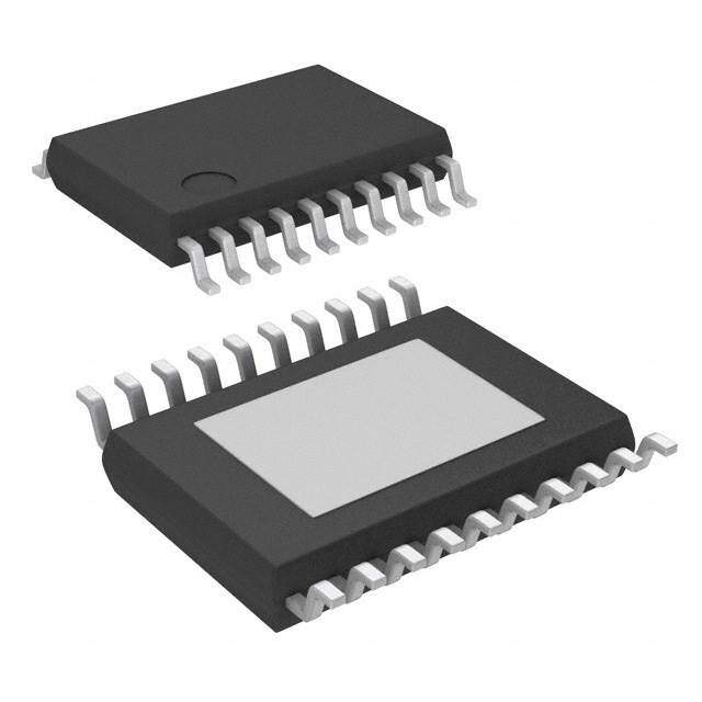
| 产品图片 |
|
| rohs | 符合RoHS无铅 / 符合限制有害物质指令(RoHS)规范要求 |
| 产品系列 | 电源管理 IC,稳压器—开关式稳压器,Texas Instruments TPS60110PWPR- |
| 数据手册 | |
| 产品型号 | TPS60110PWPR |
| PWM类型 | - |
| 产品种类 | 稳压器—开关式稳压器 |
| 供应商器件封装 | 20-HTSSOP |
| 其它名称 | 296-31986-1 |
| 包装 | 剪切带 (CT) |
| 单位重量 | 81.800 mg |
| 同步整流器 | 无 |
| 商标 | Texas Instruments |
| 安装类型 | 表面贴装 |
| 安装风格 | SMD/SMT |
| 宽度 | 4.4 mm |
| 封装 | Reel |
| 封装/外壳 | 20-TSSOP(0.173",4.40mm 宽)裸焊盘 |
| 封装/箱体 | HTSSOP-20 |
| 工作温度 | -40°C ~ 85°C |
| 工作温度范围 | - 40 C to + 85 C |
| 工厂包装数量 | 2000 |
| 开关频率 | 300 kHz |
| 拓扑结构 | Boost |
| 最大工作温度 | + 85 C |
| 最大输入电压 | 5.4 V |
| 最小工作温度 | - 40 C |
| 标准包装 | 1 |
| 电压-输入 | 2.7 V ~ 5.4 V |
| 电压-输出 | 5V |
| 电流-输出 | 300mA |
| 类型 | 升压(升压),切换电容(充电泵) |
| 系列 | TPS60110 |
| 输出数 | 1 |
| 输出电压 | 5 V |
| 输出电流 | 300 mA |
| 输出端数量 | 1 Output |
| 输出类型 | 固定 |
| 配用 | /product-detail/zh/TPS60110EVM-132/296-10946-ND/381811 |
| 频率-开关 | 300kHz |


- 商务部:美国ITC正式对集成电路等产品启动337调查
- 曝三星4nm工艺存在良率问题 高通将骁龙8 Gen1或转产台积电
- 太阳诱电将投资9.5亿元在常州建新厂生产MLCC 预计2023年完工
- 英特尔发布欧洲新工厂建设计划 深化IDM 2.0 战略
- 台积电先进制程称霸业界 有大客户加持明年业绩稳了
- 达到5530亿美元!SIA预计今年全球半导体销售额将创下新高
- 英特尔拟将自动驾驶子公司Mobileye上市 估值或超500亿美元
- 三星加码芯片和SET,合并消费电子和移动部门,撤换高东真等 CEO
- 三星电子宣布重大人事变动 还合并消费电子和移动部门
- 海关总署:前11个月进口集成电路产品价值2.52万亿元 增长14.8%


PDF Datasheet 数据手册内容提取
(cid:1)(cid:2)(cid:3)(cid:4)(cid:5)(cid:6)(cid:6)(cid:5) (cid:7)(cid:8)(cid:9)(cid:10)(cid:11)(cid:12)(cid:1)(cid:8)(cid:13) (cid:14)(cid:15)(cid:16) (cid:17)(cid:5)(cid:5)(cid:15)(cid:18)(cid:12) (cid:11)(cid:19)(cid:20)(cid:15)(cid:21)(cid:19)(cid:22)(cid:3)(cid:8) (cid:23)(cid:24)(cid:12)(cid:7)(cid:9)(cid:8) (cid:2)(cid:10)(cid:25)(cid:2) (cid:13)(cid:23)(cid:26)(cid:13)(cid:23) (cid:23)(cid:19)(cid:21)(cid:16)(cid:8)(cid:7)(cid:1)(cid:8)(cid:7) SLVS215C − JUNE 1999 − REVISED AUGUST 2008 features applications (cid:1) (cid:1) Up to 300-mA Output Current Replaces DC/DC Converters With Inductors (cid:1) Less Than 10-mV Output Voltage Ripple in pp (cid:1) − Battery-Powered Applications No Inductors Required/Low EMI − Li-Ion Battery to 5-V Conversion (cid:1) Regulated 5-V ±4% Output − Portable Instruments (cid:1) Only Four External Components Required − Battery-Powered Microprocessor (cid:1) Up to 90% Efficiency Systems (cid:1) − Miniature Equipment 2.7-V to 5.4-V Input Voltage Range − Backup-Battery Boost Converters (cid:1) 60-µA Quiescent Supply Current − PDAs (cid:1) 0.05-µA Shutdown Current − Laptops (cid:1) Load Isolated in Shutdown − Handheld Instrumentation (cid:1) − Medical Instruments Space-Saving Thermally-Enhanced TSSOP PowerPAD Package output voltage ripple (cid:1) Evaluation Module Available (TPS60110EVM−132) 5.2 description 5.15 V − 5.1 The TPS60110 step-up, regulated charge pump e g generates a 5-V ±4% output voltage from a 2.7-V olta 5.05 to 5.4-V input voltage (three alkaline, NiCd, or V NbaiMtteHr y)b.a Otteurtipeust; cour,r reonnte isl it3h0iu0m m oAr flriothmiu ma 3io-Vn utput 4.955 SKIP =COM = CLK = 0 V O VIN = 3.6 V input. Only four external capacitors are needed to − 4.9 IO = 300 mA build a complete low-noise dc/dc converter. The VO CO = 22 µF + 10 µF 4.85 push-pull operating mode of two single-ended X5R Ceramic 4.8 charge pumps assures the low output voltage 0 0.5 1 1.5 2 2.5 3 3.5 4 4.5 5 ripple as current is continuously transferred to the t − Time − µs output. From a 3-V input, the TPS60110 can start into full load with loads as low as 16 Ω. typical operating circuit The TPS60110 features either constant frequency mode to minimize noise and output voltage ripple INPUT OUTPUT 2.7 V to or the power-saving pulse-skip mode to extend 5 V 5.4 V battery life at light loads. The TPS60110 switching SKIP COMCLK 300 mA frequency is 300 kHz. The logic shutdown function CIN + IN OUT reduces the supply current to 1-µA (max) and 15 µF IN OUT + CO disconnects the load from the input. Special TPS60110 FB 33 µF current-control circuitry prevents excessive cur- C1F C1+ C2+ rent from being drawn from the battery during 2.2 µF C1− C2− C2.22F µF start-up. This dc/dc converter requires no ENABLE SYNC inductors and has low EMI. It is available in the small 20-pin TSSOP PowerPAD package OFF/ON PGND GND (PWP). Figure 1 Please be aware that an important notice concerning availability, standard warranty, and use in critical applications of TexasInstruments semiconductor products and disclaimers thereto appears at the end of this data sheet. PowerPAD is a trademark of Texas Instruments. (cid:2)(cid:7)(cid:19)(cid:13)(cid:10)(cid:23)(cid:1)(cid:22)(cid:19)(cid:21) (cid:13)(cid:12)(cid:1)(cid:12) (cid:27)(cid:28)(cid:29)(cid:30)(cid:31)(cid:18)!"(cid:27)(cid:30)(cid:28) (cid:27)# $%(cid:31)(cid:31)&(cid:28)" !# (cid:30)(cid:29) ’%()(cid:27)$!"(cid:27)(cid:30)(cid:28) *!"&+ Copyright 1999−2003 Texas Instruments Incorporated (cid:2)(cid:31)(cid:30)*%$"# $(cid:30)(cid:28)(cid:29)(cid:30)(cid:31)(cid:18) "(cid:30) #’&$(cid:27)(cid:29)(cid:27)$!"(cid:27)(cid:30)(cid:28)# ’&(cid:31) ",& "&(cid:31)(cid:18)# (cid:30)(cid:29) (cid:1)&-!# (cid:22)(cid:28)#"(cid:31)%(cid:18)&(cid:28)"# #"!(cid:28)*!(cid:31)* .!(cid:31)(cid:31)!(cid:28)"/+ (cid:2)(cid:31)(cid:30)*%$"(cid:27)(cid:30)(cid:28) ’(cid:31)(cid:30)$&##(cid:27)(cid:28)0 *(cid:30)&# (cid:28)(cid:30)" (cid:28)&$&##!(cid:31)(cid:27))/ (cid:27)(cid:28)$)%*& "&#"(cid:27)(cid:28)0 (cid:30)(cid:29) !)) ’!(cid:31)!(cid:18)&"&(cid:31)#+ POST OFFICE BOX 655303 • DALLAS, TEXAS 75265 1
(cid:1)(cid:2)(cid:3)(cid:4)(cid:5)(cid:6)(cid:6)(cid:5) (cid:7)(cid:8)(cid:9)(cid:10)(cid:11)(cid:12)(cid:1)(cid:8)(cid:13) (cid:14)(cid:15)(cid:16) (cid:17)(cid:5)(cid:5)(cid:15)(cid:18)(cid:12) (cid:11)(cid:19)(cid:20)(cid:15)(cid:21)(cid:19)(cid:22)(cid:3)(cid:8) (cid:23)(cid:24)(cid:12)(cid:7)(cid:9)(cid:8) (cid:2)(cid:10)(cid:25)(cid:2) (cid:13)(cid:23)(cid:26)(cid:13)(cid:23) (cid:23)(cid:19)(cid:21)(cid:16)(cid:8)(cid:7)(cid:1)(cid:8)(cid:7) SLVS215C − JUNE 1999 − REVISED AUGUST 2008 PWP PACKAGE (TOP VIEW) GND 1 20 GND SYNC 2 19 CLK ENABLE 3 18 COM Thermal FB 4 17 SKIP Pad OUT 5 16 OUT C1+ 6 15 C2+ IN 7 14 IN C1− 8 13 C2− PGND 9 12 PGND PGND 10 11 PGND Figure 2. Bottom View of PWP Package, Showing the Thermal Pad AVAILABLE OPTIONS PACKAGE TSSOP† (PWP) TPS60110PWP †This package is available taped and reeled. To order this packaging option, add an R suffix to the part number (e.g., TPS60110PWPR). Terminal Functions TERMINAL II//OO DDEESSCCRRIIPPTTIIOONN NAME NO. CLK 19 I Input for external clock signal. If the internal clock is used, connect this terminal to GND. C1+ 6 Positive terminal of the charge-pump capacitor C1F C1− 8 Negative terminal of the charge-pump capacitor C1F C2+ 15 Positive terminal of the charge-pump capacitor C2F C2− 13 Negative terminal of the charge-pump capacitor C2F COM 18 I Mode selection. When COM is logic low the charge pump operates in push-pull mode to minimize output ripple. When COM is connected to IN the regulator operates in single-ended mode requiring only one flying capacitor. ENABLE 3 I ENABLE Input. The device turns off, the output disconnects from the input, and the supply current decreases to 0.05 µA when ENABLE is a logic low. ENABLE High may only be applied when VIN is inside the recommended operating range. FB 4 I FEEDBACK input. Connect FB to OUT as close to the load as possible to achieve best regulation. Resistive divider is on-chip to match internal reference voltage of 1.22 V. GND 1, 20 GROUND. Analog ground for internal reference and control circuitry. Connect to PGND through a short trace. IN 7, 14 I Supply Input. Connect to an input supply in the 2.7-V to 5.4-V range. Bypass IN to GND with a (CO/2) µF capacitor. Connect both INs through a short trace. OUT 5, 16 O Regulated 5-V power output. Connect both OUTs through a short trace and bypass OUT to GND with the output filter capacitor CO. PGND 9−12 PGND power ground. Charge-pump current flows through this pin. Connect all PGNDs together. SKIP 17 I Mode selection. When SKIP is logic low, the charge pump operates in constant-frequency mode. Output ripple and noise are minimized in this mode. When SKIP is connect to IN, the device operates in pulse skip mode. Quiescent current is lowest in this mode. SYNC 2 I Selection for external clock signal. Connect to GND to use the internally generated clock signal. Connect to IN for external synchronization. In this case, the clock signal needs to be fed through CLK. PowerPAD Must be soldered to achieve appropriate power dissipation. Should be connected to PGND. 2 POST OFFICE BOX 655303 • DALLAS, TEXAS 75265
(cid:1)(cid:2)(cid:3)(cid:4)(cid:5)(cid:6)(cid:6)(cid:5) (cid:7)(cid:8)(cid:9)(cid:10)(cid:11)(cid:12)(cid:1)(cid:8)(cid:13) (cid:14)(cid:15)(cid:16) (cid:17)(cid:5)(cid:5)(cid:15)(cid:18)(cid:12) (cid:11)(cid:19)(cid:20)(cid:15)(cid:21)(cid:19)(cid:22)(cid:3)(cid:8) (cid:23)(cid:24)(cid:12)(cid:7)(cid:9)(cid:8) (cid:2)(cid:10)(cid:25)(cid:2) (cid:13)(cid:23)(cid:26)(cid:13)(cid:23) (cid:23)(cid:19)(cid:21)(cid:16)(cid:8)(cid:7)(cid:1)(cid:8)(cid:7) SLVS215C − JUNE 1999 − REVISED AUGUST 2008 absolute maximum ratings (unless otherwise noted)†‡ Input voltage range, VI (IN, OUT, ENABLE, SKIP, COM, CLK, FB, SYNC) . . . . . . . . . . . . . . . . −0.3 V to 5.5 V Differential input voltage, VID (C1+, C2+ to GND) . . . . . . . . . . . . . . . . . . . . . . . . . . . . . . −0.3 V to (VO + 0.3 V) Differential input voltage, VID (C1−, C2− to GND) . . . . . . . . . . . . . . . . . . . . . . . . . . . . . . −0.3 V to (VIN + 0.3 V) Continuous total power dissipation . . . . . . . . . . . . . . . . . . . . . . . . . . . . . . . . . . . . See Dissipation Rating Tables Continuous output current . . . . . . . . . . . . . . . . . . . . . . . . . . . . . . . . . . . . . . . . . . . . . . . . . . . . . . . . . . . . . . . . 400 mA Storage temperature range, T . . . . . . . . . . . . . . . . . . . . . . . . . . . . . . . . . . . . . . . . . . . . . . . . . . . −55°C to 150°C stg Lead temperature 1,6 mm (1/16 inch) from case for 10s . . . . . . . . . . . . . . . . . . . . . . . . . . . . . . . . . . . . . . . 260°C Maximum junction temperature, T . . . . . . . . . . . . . . . . . . . . . . . . . . . . . . . . . . . . . . . . . . . . . . . . . . . . . . . . . 150°C J †Stresses beyond those listed under “absolute maximum ratings” may cause permanent damage to the device. These are stress ratings only, and functional operation of the device at these or any other conditions beyond those indicated under “recommended operating conditions” is not implied. Exposure to absolute-maximum-rated conditions for extended periods may affect device reliability. ‡VENABLE, VSKIP, VCOM, VCLK and VSYNC can exceed VIN up to the maximum rated voltage without increasing the leakage current drawn by these mode select inputs. PACKAGE DISSIPATION RATINGS TTAA ≤≤ 2255°CC DDEERRAATTIINNGG FFAACCTTOORR TTAA == 7700°CC TTAA == 8855°CC PPAACCKKAAGGEE POWER RATING ABOVE TA = 25°C§§ POWER RATING POWER RATING PWP 3 W 30.3 mW/°C 1.66 W 1.21 W §The thermal resistance junction to ambient of the 20-pin TSSOP PowerPAD package RθJA = 33°C/W (soldered PowerPAD using thermal vias). PowerPAD packages are modeled and tested using PWB boards recommended in the PowerPAD Application Report, SLMA0002. PowerPAD packages are designed for board mounting with the die pad soldered to a copper pad patterned on the board. POST OFFICE BOX 655303 • DALLAS, TEXAS 75265 3
(cid:1)(cid:2)(cid:3)(cid:4)(cid:5)(cid:6)(cid:6)(cid:5) (cid:7)(cid:8)(cid:9)(cid:10)(cid:11)(cid:12)(cid:1)(cid:8)(cid:13) (cid:14)(cid:15)(cid:16) (cid:17)(cid:5)(cid:5)(cid:15)(cid:18)(cid:12) (cid:11)(cid:19)(cid:20)(cid:15)(cid:21)(cid:19)(cid:22)(cid:3)(cid:8) (cid:23)(cid:24)(cid:12)(cid:7)(cid:9)(cid:8) (cid:2)(cid:10)(cid:25)(cid:2) (cid:13)(cid:23)(cid:26)(cid:13)(cid:23) (cid:23)(cid:19)(cid:21)(cid:16)(cid:8)(cid:7)(cid:1)(cid:8)(cid:7) SLVS215C − JUNE 1999 − REVISED AUGUST 2008 electrical characteristics at C = 15 µF, C = C = 2.2 µF†, C = 33 µF, T = −40°C to 85°C, IN 1F 2F O C V = 3 V, V = V , V = V , V = V or 0 V and V = V = V = 0 V (unless otherwise IN FB O ENABLE IN SKIP IN COM CLK SYNC noted) PARAMETER TEST CONDITIONS MIN TYP MAX UNIT VIN Input voltage 2.7 5.4 V IO(MAX) Maximum output current 300 mA 2.7 V < VIN < 3 V, 0 < IO < 150 mA, 4.8 5 5.2 VO(Start-Up) = 5 V, TC = 25°C VVOO OOuuttppuutt vvoollttaaggee VV 3 V < VIN < 5 V, 0 < IO < 300 mA 4.8 5 5.2 5 V < VIN < 5.4 V, 0 < IO < 300 mA 4.8 5 5.25 VO(RIP) Output voltage ripple IO = 300 mA, V(SKIP) = 0 V 10‡ mVPP IO(LEAK) Output leakage current VIN = 3.6 V, V(ENABLE) = 0 V 1 µA V(SKIP) = VIN = 3.6 V 60 90 µA IIQQ QQuuiieesscceenntt ccuurrrreenntt ((nnoo--llooaadd iinnppuutt ccuurrrreenntt)) V(SKIP) = 0 V, VIN = 3.6 V 2.8 mA IDD(SDN) Shutdown supply current VIN = 3.6 V, V(ENABLE) = 0 V 0.05 1 µA fOSC(int) Internal switching frequency VIN = 3.6 V 200 300 400 kHz fOSC(ext) External clock frequency V(SYNC) = VIN, VIN = 2.7 V to 5.4 V 400 600 800 kHz External clock duty cycle V(SYNC) = VIN, VIN= 2.7V to 5.4 V 20% 80% Efficiency IO = 150 mA 80% Input voltage low, 0.3 × VINL ENABLE, SKIP, COM, CLK, SYNC VIN = 2.7 V VIN V Input voltage high, 0.7 × VINH ENABLE, SKIP, COM, CLK, SYNC VIN = 5.4 V VIN V II(LEAK) IEnNpuAtB leLaEk, aSgKeI Pc,u CrrOenMt,, CLK, SYNC VV((ESNYNABCL) E=) V =( GVN(SDK)I Por) V= IVN(COM) = V(CLK) = 0.01 0.1 µA Output load regulation VO = 5 V, 1 mA < IO < 300 mA, TC = 25°C 0.002 %/mA 3 V < VIN < 5 V, VO = 5 V, Output line regulation 0.6 %/V IO = 150 mA, TC = 25°C Short circuit current VIN = 3.6 V, VO = 0 V, TC = 25°C 150 mA †Use only ceramic capacitors with X5R or X7R dielectric as flying capacitors. ‡Achieved with CO = 22 µF + 10 µF X5R dielectric ceramic capacitor 4 POST OFFICE BOX 655303 • DALLAS, TEXAS 75265
(cid:1)(cid:2)(cid:3)(cid:4)(cid:5)(cid:6)(cid:6)(cid:5) (cid:7)(cid:8)(cid:9)(cid:10)(cid:11)(cid:12)(cid:1)(cid:8)(cid:13) (cid:14)(cid:15)(cid:16) (cid:17)(cid:5)(cid:5)(cid:15)(cid:18)(cid:12) (cid:11)(cid:19)(cid:20)(cid:15)(cid:21)(cid:19)(cid:22)(cid:3)(cid:8) (cid:23)(cid:24)(cid:12)(cid:7)(cid:9)(cid:8) (cid:2)(cid:10)(cid:25)(cid:2) (cid:13)(cid:23)(cid:26)(cid:13)(cid:23) (cid:23)(cid:19)(cid:21)(cid:16)(cid:8)(cid:7)(cid:1)(cid:8)(cid:7) SLVS215C − JUNE 1999 − REVISED AUGUST 2008 TYPICAL CHARACTERISTICS† EFFICIENCY EFFICIENCY vs vs OUTPUT CURRENT OUTPUT CURRENT 100 100 VIN = 2.7 V V(SKIP) = 0 V VIN = 2.7 V 90 90 VIN = 3 V VIN = 3 V 80 80 70 70 Efficiency − % 546000 VIN = 3.3 V VIN = 3.6 V Efficiency − % 546000 VIN = 3.6 V VIN = 3.3 V 30 30 20 20 10 10 V(SKIP) = VIN 0 0 0.1 1 10 100 1000 1 10 100 1000 IO − Output Current − mA IO − Output Current − mA Figure 3 Figure 4 QUIESCENT SUPPLY CURRENT QUIESCENT SUPPLY CURRENT vs vs INPUT VOLTAGE INPUT VOLTAGE 90 3.6 V(SKIP) = VIN V(SKIP) = 0 V 85 3.4 IO = 300 mA A A µ− 80 − m 3.2 nt nt urre 75 urre 3 C C y 70 y 2.8 pl pl up 65 up 2.6 S S ent 60 ent 2.4 c c s s e e ui 55 ui 2.2 Q Q − Q 50 − Q 2 I I 45 1.8 40 1.6 2.5 3 3.5 4 4.5 5 5.5 2.5 3 3.5 4 4.5 5 5.5 VIN − Input Voltage − V VIN − Input Voltage − V Figure 5 Figure 6 †TC = 25°C, VCOM = VSYNC = 0 V, CIN = 15 µF, C1F = C2F = 2.2 µF, CO = 33 µF, unless otherwise noted POST OFFICE BOX 655303 • DALLAS, TEXAS 75265 5
(cid:1)(cid:2)(cid:3)(cid:4)(cid:5)(cid:6)(cid:6)(cid:5) (cid:7)(cid:8)(cid:9)(cid:10)(cid:11)(cid:12)(cid:1)(cid:8)(cid:13) (cid:14)(cid:15)(cid:16) (cid:17)(cid:5)(cid:5)(cid:15)(cid:18)(cid:12) (cid:11)(cid:19)(cid:20)(cid:15)(cid:21)(cid:19)(cid:22)(cid:3)(cid:8) (cid:23)(cid:24)(cid:12)(cid:7)(cid:9)(cid:8) (cid:2)(cid:10)(cid:25)(cid:2) (cid:13)(cid:23)(cid:26)(cid:13)(cid:23) (cid:23)(cid:19)(cid:21)(cid:16)(cid:8)(cid:7)(cid:1)(cid:8)(cid:7) SLVS215C − JUNE 1999 − REVISED AUGUST 2008 TYPICAL CHARACTERISTICS† OUTPUT VOLTAGE OUTPUT VOLTAGE vs vs OUTPUT CURRENT OUTPUT CURRENT 5.3 5.3 V(SKIP) = 0 V V(SKIP) = VIN 5.2 5.2 VIN = 5.4 V VIN = 5.4 V Voltage − V 5.1 VIN = 4 VVIN = 3.6 V Voltage − V 5.1 VIN = 4 VVIN = 3.6 V − Output 4.95 VIN = 3 V − Output 4.95 VIN = 3 V O O V V VIN = 2.7 V VIN = 2.7 V 4.8 4.8 4.7 4.7 1 10 100 1000 1 10 100 1000 IO − Output Current − mA IO − Output Current − mA Figure 7 Figure 8 OUTPUT VOLTAGE OUTPUT VOLTAGE vs vs INPUT VOLTAGE INPUT VOLTAGE 5.1 5.1 V(SKIP) = 0 V V(SKIP) = VIN 5.08 5.08 IO = 300 mA 5.06 IO = 300 mA 5.06 V V Voltage − 55..0024 IO = 150 mA Voltage − 55..0024 − Output 4.958 IO = 1 mA to 10 mA − Output 4.958 O O V 4.96 V 4.96 4.94 4.94 4.92 4.92 4.9 4.9 2.5 3 3.5 4 4.5 5 5.5 2.5 3 3.5 4 4.5 5 5.5 VIN − Input Voltage − V VIN − Input Voltage − V Figure 9 Figure 10 †TC = 25°C, VCOM = VSYNC = 0 V, CIN = 15 µF, C1F = C2F = 2.2 µF, CO = 33 µF, unless otherwise noted 6 POST OFFICE BOX 655303 • DALLAS, TEXAS 75265
(cid:1)(cid:2)(cid:3)(cid:4)(cid:5)(cid:6)(cid:6)(cid:5) (cid:7)(cid:8)(cid:9)(cid:10)(cid:11)(cid:12)(cid:1)(cid:8)(cid:13) (cid:14)(cid:15)(cid:16) (cid:17)(cid:5)(cid:5)(cid:15)(cid:18)(cid:12) (cid:11)(cid:19)(cid:20)(cid:15)(cid:21)(cid:19)(cid:22)(cid:3)(cid:8) (cid:23)(cid:24)(cid:12)(cid:7)(cid:9)(cid:8) (cid:2)(cid:10)(cid:25)(cid:2) (cid:13)(cid:23)(cid:26)(cid:13)(cid:23) (cid:23)(cid:19)(cid:21)(cid:16)(cid:8)(cid:7)(cid:1)(cid:8)(cid:7) SLVS215C − JUNE 1999 − REVISED AUGUST 2008 TYPICAL CHARACTERISTICS† OUTPUT VOLTAGE OUTPUT VOLTAGE vs vs TIME TIME 5.05 5.07 V(SKIP) = 0 V Constant Pulse-Skip Mode VIN = 3.6 V Frequency IO = 150 mA Mode 5.04 CO = 22 µF + 10 µF V X5R ceramic V 5.05 ge − ge − ut Volta 5.03 ut Volta 5.03 p p ut ut O O − − O O V 5.02 V 5.01 V(SKIP) = VIN VIN = 3.6 V IO = 150 mA 5.01 4.99 0 2 4 6 8 10 0 10 20 30 40 50 t − Time − µs t − Time − µs Figure 11 Figure 12 LOAD TRANSIENT RESPONSE LOAD TRANSIENT RESPONSE − Output Voltage − VVO 5555....00002453 − Output Voltage − VVO 5555....00002684 IVO(S =K 1IP0 )m =A V tINo 3=0 30. 6m VA Pulse-Skip Mode 5.01 5 mA mA Output Current − 426000000 IVVOI(NS =K =1I P03 ).m6 = VA 0 tVo 300 mA CFMrooendqseuteanncty Output Current − 426000000 − O 0 − O 0 I 0 2 4 6 8 10 12 14 16 18 20 I 0 2 4 6 8 10 12 14 16 18 20 t − Time − ms t − Time − ms Figure 13 Figure 14 †TC = 25°C, VCOM = VSYNC = 0 V, CIN = 15 µF, C1F = C2F = 2.2 µF, CO = 33 µF, unless otherwise noted POST OFFICE BOX 655303 • DALLAS, TEXAS 75265 7
(cid:1)(cid:2)(cid:3)(cid:4)(cid:5)(cid:6)(cid:6)(cid:5) (cid:7)(cid:8)(cid:9)(cid:10)(cid:11)(cid:12)(cid:1)(cid:8)(cid:13) (cid:14)(cid:15)(cid:16) (cid:17)(cid:5)(cid:5)(cid:15)(cid:18)(cid:12) (cid:11)(cid:19)(cid:20)(cid:15)(cid:21)(cid:19)(cid:22)(cid:3)(cid:8) (cid:23)(cid:24)(cid:12)(cid:7)(cid:9)(cid:8) (cid:2)(cid:10)(cid:25)(cid:2) (cid:13)(cid:23)(cid:26)(cid:13)(cid:23) (cid:23)(cid:19)(cid:21)(cid:16)(cid:8)(cid:7)(cid:1)(cid:8)(cid:7) SLVS215C − JUNE 1999 − REVISED AUGUST 2008 TYPICAL CHARACTERISTICS† LINE TRANSIENT RESPONSE LINE TRANSIENT RESPONSE Output Voltage − V 555...000468 IVO(S =K 1IP50) =m 0A V CFMrooendqseuteanncty Output Voltage − V 555...000468 IVO(S =K 1IP50) =m VAIN Pulse-Skip Mode − 5.02 − 5.02 VO VO 5 5 − Input Voltage − V 543 − Input Voltage − V 543 VIN 20 1 2 3 4 5 6 7 8 9 10 VIN 20 1 2 3 4 5 6 7 8 9 10 t − Time − ms t − Time − ms Figure 15 Figure 16 FREQUENCY SPECTRUM FREQUENCY SPECTRUM CONSTANT FREQUENCY MODE‡ PULSE-SKIP MODE‡ 90 100 V(SKIP) = 0 V V(SKIP) = VIN 80 VIN = 3 V VIN = 3 V IO = 150 mA IO = 150 mA 70 RBW = 300 Hz 80 RBW = 300 Hz 60 V V µ µ 60 B B d 50 d − − ut ut p 40 p ut ut 40 O O 30 20 20 10 0 0 0 2.5 5 7.5 10 0 2.5 5 7.5 10 f − Frequency − MHz f − Frequency − MHz Figure 17 Figure 18 †TC = 25°C, VCOM = VSYNC = 0 V, CIN = 15 µF, C1F = C2F = 2.2 µF, CO = 33 µF, unless otherwise noted ‡Test circuit: TPS60110EVM−132 8 POST OFFICE BOX 655303 • DALLAS, TEXAS 75265
(cid:1)(cid:2)(cid:3)(cid:4)(cid:5)(cid:6)(cid:6)(cid:5) (cid:7)(cid:8)(cid:9)(cid:10)(cid:11)(cid:12)(cid:1)(cid:8)(cid:13) (cid:14)(cid:15)(cid:16) (cid:17)(cid:5)(cid:5)(cid:15)(cid:18)(cid:12) (cid:11)(cid:19)(cid:20)(cid:15)(cid:21)(cid:19)(cid:22)(cid:3)(cid:8) (cid:23)(cid:24)(cid:12)(cid:7)(cid:9)(cid:8) (cid:2)(cid:10)(cid:25)(cid:2) (cid:13)(cid:23)(cid:26)(cid:13)(cid:23) (cid:23)(cid:19)(cid:21)(cid:16)(cid:8)(cid:7)(cid:1)(cid:8)(cid:7) SLVS215C − JUNE 1999 − REVISED AUGUST 2008 TYPICAL CHARACTERISTICS† FREQUENCY SPECTRUM FREQUENCY SPECTRUM CONSTANT FREQUENCY MODE‡ PULSE-SKIP MODE‡ 90 90 V(SKIP) = 0 V V(SKIP) = VIN 80 VIN = 3 V 80 VIN = 3 V IO = 10 mA IO = 10 mA 70 RBW = 300 Hz 70 RBW = 300 Hz 60 60 V V µ µ B B d 50 d 50 − − put 40 put 40 ut ut O O 30 30 20 20 10 10 0 0 0 2.5 5 7.5 10 0 2.5 5 7.5 10 f − Frequency − MHz f − Frequency − MHz Figure 19 Figure 20 EFFICIENCY vs INPUT VOLTAGE START-UP TIMING 100 6 R0 = 16.5 Ω 90 VIN = 3 V 5 80 70 Skip = High e − V 4 g % a − 60 Skip = Low olt 3 ncy 50 ut V Enable e p ci ut 2 Effi 40 − O OUTPUT 30 VO 1 20 0 10 0 −1 2.5 3 3.5 4 4.5 5 5.5 0 200 400 600 800 1000 1200 VIN − Input Voltage − V t − Time −µs Figure 21 Figure 22 †TC = 25°C, VCOM = VSYNC = 0 V, CIN = 15 µF, C1F = C2F = 2.2 µF, CO = 33 µF, unless otherwise noted ‡Test circuit: TPS60110EVM−132 POST OFFICE BOX 655303 • DALLAS, TEXAS 75265 9
(cid:1)(cid:2)(cid:3)(cid:4)(cid:5)(cid:6)(cid:6)(cid:5) (cid:7)(cid:8)(cid:9)(cid:10)(cid:11)(cid:12)(cid:1)(cid:8)(cid:13) (cid:14)(cid:15)(cid:16) (cid:17)(cid:5)(cid:5)(cid:15)(cid:18)(cid:12) (cid:11)(cid:19)(cid:20)(cid:15)(cid:21)(cid:19)(cid:22)(cid:3)(cid:8) (cid:23)(cid:24)(cid:12)(cid:7)(cid:9)(cid:8) (cid:2)(cid:10)(cid:25)(cid:2) (cid:13)(cid:23)(cid:26)(cid:13)(cid:23) (cid:23)(cid:19)(cid:21)(cid:16)(cid:8)(cid:7)(cid:1)(cid:8)(cid:7) SLVS215C − JUNE 1999 − REVISED AUGUST 2008 detailed description operating principle The TPS60110 charge pump provides a regulated 5-V output from a 2.7-V to 5.4-V input. It delivers a maximum load current of 300 mA. Designed specifically for space critical battery powered applications, the complete charge pump circuit requires only four external capacitors. The circuit can be optimized for highest efficiency at light loads or lowest output noise. The TPS60110 consists of an oscillator, a 1.22-V bandgap reference, an internal resistive feedback circuit, an error amplifier, high current MOSFET switches, a shutdown/start-up circuit, and a control circuit (Figure 23) CHARGE PUMP 1 0° IN OSCILLATOR T11 T12 180° C1+ C1F C1− T13 T14 SKIP OUT COM PGND CONTROL CIRCUIT FB CLK SYNC − CHARGE PUMP 2 + IN VREF+− T21 T22 C2+ C2F SHUTDOWN/ − C2− ENABLE START-UP + T23 T24 CONTROL +− 0.8 × VIN OUT PGND GND Figure 23. Functional Block Diagram TPS60110 The oscillator runs at a 50% duty cycle. The device consists of two single-ended charge pumps which operate with 180° phase shift. Each single ended charge pump transfers charge into its transfer capacitor (C ) in one xF half of the period. During the other half of the period (transfer phase), C is placed in series with the input to xF transfer its charge to C . While one single-ended charge pump is in the charge phase, the other one is in the O transfer phase. This operation specifies an almost constant output current which ensures a low output ripple. If the clock were to run continuously, this process would eventually generate an output voltage equal to two times the input voltage (hence the name doubler). In order to provide a regulated fixed output voltage of 5 V, the TPS60110 uses either pulse-skip mode or constant-frequency mode. Pulse-skip mode and constant-frequency mode are externally selected via the SKIP input pin. 10 POST OFFICE BOX 655303 • DALLAS, TEXAS 75265
(cid:1)(cid:2)(cid:3)(cid:4)(cid:5)(cid:6)(cid:6)(cid:5) (cid:7)(cid:8)(cid:9)(cid:10)(cid:11)(cid:12)(cid:1)(cid:8)(cid:13) (cid:14)(cid:15)(cid:16) (cid:17)(cid:5)(cid:5)(cid:15)(cid:18)(cid:12) (cid:11)(cid:19)(cid:20)(cid:15)(cid:21)(cid:19)(cid:22)(cid:3)(cid:8) (cid:23)(cid:24)(cid:12)(cid:7)(cid:9)(cid:8) (cid:2)(cid:10)(cid:25)(cid:2) (cid:13)(cid:23)(cid:26)(cid:13)(cid:23) (cid:23)(cid:19)(cid:21)(cid:16)(cid:8)(cid:7)(cid:1)(cid:8)(cid:7) SLVS215C − JUNE 1999 − REVISED AUGUST 2008 detailed description (continued) start-up procedure During start-up, i.e. when ENABLE is set from logic low to logic high, the switches T12 and T14 (charge pump 1), and the switches T22 and T24 (charge pump 2) are conducting to charge up the output capacitor until the output voltage V reaches 0.8×V . When the start-up comparator detects this limit, the IC begins to operate O IN in the mode selected with SKIP and COM. This start-up charging of the output capacitor specifies a short start-up time and eliminates the need for a Schottky diode between IN and OUT. pulse-skip mode In pulse-skip mode (SKIP = high), the error amplifier disables switching of the power stages when it detects an output higher than 5 V. The oscillator halts. The IC then skips switching cycles until the output voltage drops below 5 V. Then the error amplifier reactivates the oscillator and switching of the power stages starts again. The pulse-skip regulation mode minimizes operating current because it does not switch continuously and deactivates all functions except bandgap reference and error amplifier when the output is higher than 5 V. When switching is disabled from the error amplifier, the load is also isolated from the input. SKIP is a logic input and should not remain floating. The typical operating circuit of the TPS60110 in pulse skip mode is shown in Figure 1. constant-frequency mode When SKIP is low, the charge pump runs continuously at the frequency f . The control circuit, fed from the OSC error amplifier, controls the charge on C and C by driving the gates of the FETs T /T and T /T , 1F 2F 12 13 22 23 respectively. When the output voltage falls, the gate drive increases, resulting in a larger voltage across C 1F and C . This regulation scheme minimizes output ripple. Since the device switches continuously, the output 2F noise contains well-defined frequency components, and the circuit requires smaller external capacitors for a given output ripple. However, constant-frequency mode, due to higher operating current, is less efficient at light loads than pulse-skip mode. SKIP COMCLK INPUT OUTPUT IN OUT 2.7 V to 5.4 V 5 V 300 mA IN OUT + TPS60110 FB 15C IµNF + 2.2C µ1FF C1+ C2+ C2F CO = 33 µF C1− C2− 2.2 µF ENABLE SYNC OFF/ON PGND GND Figure 24. Typical Operating Circuit TPS60110 in Constant Frequency Mode Table 1. Tradeoffs Between Operating Modes FEATURE PULSE-SKIP MODE CONSTANT-FREQUENCY MODE (SKIP = High) (SKIP = Low) Best light-load efficiency X Smallest external component size for a given output ripple X Output ripple amplitude Small amplitude Very small amplitude Output ripple frequency Variable Constant Load regulation Very good Good NOTE: Even in pulse-skip mode the output ripple amplitude is small if the push-pull operating mode is selected via COM. POST OFFICE BOX 655303 • DALLAS, TEXAS 75265 11
(cid:1)(cid:2)(cid:3)(cid:4)(cid:5)(cid:6)(cid:6)(cid:5) (cid:7)(cid:8)(cid:9)(cid:10)(cid:11)(cid:12)(cid:1)(cid:8)(cid:13) (cid:14)(cid:15)(cid:16) (cid:17)(cid:5)(cid:5)(cid:15)(cid:18)(cid:12) (cid:11)(cid:19)(cid:20)(cid:15)(cid:21)(cid:19)(cid:22)(cid:3)(cid:8) (cid:23)(cid:24)(cid:12)(cid:7)(cid:9)(cid:8) (cid:2)(cid:10)(cid:25)(cid:2) (cid:13)(cid:23)(cid:26)(cid:13)(cid:23) (cid:23)(cid:19)(cid:21)(cid:16)(cid:8)(cid:7)(cid:1)(cid:8)(cid:7) SLVS215C − JUNE 1999 − REVISED AUGUST 2008 detailed description (continued) push-pull operating mode In push-pull operating mode (COM = low), the two single-ended charge pumps operate with 180° phase shift. The oscillator signal has a 50% duty cycle. Each single-ended charge pump transfers charge into its transfer capacitor (C ) in one-half of the period. During the other half of the period (transfer phase), C is placed in xF xF series with the input to transfer its charge to C . While one single-ended charge pump is in the charge phase, O the other one is in the transfer phase. This operation specifies an almost constant output current which ensures a low output ripple. COM is a logic input and should not remain floating. The typical operating circuit of the TPS60110 in push-pull mode is shown in Figure 1 and Figure 24. single-ended operating mode When COM is high, the device runs in single-ended operating mode. The two single-ended charge pumps operate in parallel without phase shift. They transfer charge into the transfer capacitor (C ) in one half of the F period. During the other half of the period (transfer phase), C is placed in series with the input to transfer its F charge to C . In single-ended operating mode only one transfer capacitor (C = C + C ) is required, resulting O F 1F 2F in less board space. SKIP COMCLK INPUT OUTPUT IN OUT 2.7 V to 5.4 V 5 V 300 mA IN OUT + TPS60110 FB CIN + C1+ C2+ CO = 33 µF 15 µF C1− C2− ENABLE SYNC OFF/ON PGND GND CF = 4.7 µF Figure 25. Typical Operating Circuit TPS60110 in Single-Ended Operating Mode Table 2. Tradeoffs Between Operating Modes FEATURE PUSH-PULL MODE SINGLE-ENDED MODE (COM = Low) (COM = High) Output ripple amplitude Small amplitude Large amplitude Smallest board space X 12 POST OFFICE BOX 655303 • DALLAS, TEXAS 75265
(cid:1)(cid:2)(cid:3)(cid:4)(cid:5)(cid:6)(cid:6)(cid:5) (cid:7)(cid:8)(cid:9)(cid:10)(cid:11)(cid:12)(cid:1)(cid:8)(cid:13) (cid:14)(cid:15)(cid:16) (cid:17)(cid:5)(cid:5)(cid:15)(cid:18)(cid:12) (cid:11)(cid:19)(cid:20)(cid:15)(cid:21)(cid:19)(cid:22)(cid:3)(cid:8) (cid:23)(cid:24)(cid:12)(cid:7)(cid:9)(cid:8) (cid:2)(cid:10)(cid:25)(cid:2) (cid:13)(cid:23)(cid:26)(cid:13)(cid:23) (cid:23)(cid:19)(cid:21)(cid:16)(cid:8)(cid:7)(cid:1)(cid:8)(cid:7) SLVS215C − JUNE 1999 − REVISED AUGUST 2008 detailed description (continued) shutdown Driving ENABLE low places the device in shutdown mode. This disables all switches, the oscillator, and control logic. The device typically draws 0.05-µA (1-µA max) of supply current in this mode. Leakage current drawn from the output is as low as 1 µA max. The device exits shutdown once ENABLE is high. The typical no-load shutdown exit time is 20 µs. When the device is in shutdown, the load is isolated from the input and the output is high impedance. external clock signal If the device operates at a user defined frequency, an external clock signal can be used. Therefore, SYNC needs to be connected to IN and the external oscillator signal can drive CLK. The maximum external frequency is limited to 800 kHz. The switching frequency of the converter is half of the external oscillator frequency. It is recommended to operate the charge pump in constant-frequency mode if an external clock signal is used so that the output noise contains only well-defined frequency components. External Clock SKIP COMCLK INPUT OUTPUT IN OUT 2.7 V to 5.4 V 5 V 300 mA IN OUT + TPS60110 FB 15C IµNF + 2.2C µ1FF C1+ C2+ C2F CO = 33 µF C1− C2− 2.2 µF ENABLE SYNC OFF/ON PGND GND Figure 26. Typical Operating Circuit TPS60110 With External Synchronization POST OFFICE BOX 655303 • DALLAS, TEXAS 75265 13
(cid:1)(cid:2)(cid:3)(cid:4)(cid:5)(cid:6)(cid:6)(cid:5) (cid:7)(cid:8)(cid:9)(cid:10)(cid:11)(cid:12)(cid:1)(cid:8)(cid:13) (cid:14)(cid:15)(cid:16) (cid:17)(cid:5)(cid:5)(cid:15)(cid:18)(cid:12) (cid:11)(cid:19)(cid:20)(cid:15)(cid:21)(cid:19)(cid:22)(cid:3)(cid:8) (cid:23)(cid:24)(cid:12)(cid:7)(cid:9)(cid:8) (cid:2)(cid:10)(cid:25)(cid:2) (cid:13)(cid:23)(cid:26)(cid:13)(cid:23) (cid:23)(cid:19)(cid:21)(cid:16)(cid:8)(cid:7)(cid:1)(cid:8)(cid:7) SLVS215C − JUNE 1999 − REVISED AUGUST 2008 APPLICATION INFORMATION capacitor selection The TPS60110 requires only four external capacitors as shown in the basic application circuit. Their values are closely linked to the output current capacity, output noise requirements, and mode of operation. Generally, the transfer capacitors (C ) is the smallest. xF The input capacitor improves system efficiency by reducing the input impedance and stabilizes the input current. C is recommended to be about two to four times as large as C . IN xF The output capacitor (C ) can be selected from 8-times to 50-times larger than C , depending on the mode O xF of operation and ripple tolerance†. Tables 3 and 4 show capacitor values recommended for low quiescent-current operation (pulse-skip mode) and for low output voltage ripple operation (constant-frequency mode). A recommendation is given for smallest size. Table 3. Recommended Capacitor Values for Low Quiescent-Current Operation† (pulse-skip mode) CIN CO OUTPUT V[[VVIINN]] IIOO [[mmAA]] [µF] C[[µµxxFFFF]] [µF] RRVIIPPOPPLLLTEEA GVVPPEPP TANTALUM CERAMIC TANTALUM CERAMIC [mV] 3.6 225 15 2.2 33 145 3.6 225 4.7 + 10, (X5R) 2.2 22 + 10, (X5R) 55 3.6 300 15 2.2 33 135 3.6 300 4.7 + 10, (X5R) 2.2 22 + 10, (X5R) 75 †All measurements are done with additional 1-µF X7R ceramic capacitors at input and output. Table 4. Recommended Capacitor Values for Low Output Voltage Ripple Operation† (constant-frequency mode) CIN CO OUTPUT VIINN IOO [µF] CxxFF [µF] VOLTAGE [[VV]] [[mmAA]] [[µµFF]] RRIIPPPPLLEE VVPPPP TANTALUM CERAMIC TANTALUM CERAMIC [mV] 3.6 225 15 2.2 33 17 3.6 225 4.7 + 10, (X5R) 2.2 22 + 10, (X5R) 6 3.6 300 15 2.2 33 22 3.6 300 4.7 + 10, (X5R) 2.2 22 + 10, (X5R) 8 †All measurements are done with additional 1-µF X7R ceramic capacitors at input and output. †In constant-frequency mode always select CO ≥ 33 µF 14 POST OFFICE BOX 655303 • DALLAS, TEXAS 75265
(cid:1)(cid:2)(cid:3)(cid:4)(cid:5)(cid:6)(cid:6)(cid:5) (cid:7)(cid:8)(cid:9)(cid:10)(cid:11)(cid:12)(cid:1)(cid:8)(cid:13) (cid:14)(cid:15)(cid:16) (cid:17)(cid:5)(cid:5)(cid:15)(cid:18)(cid:12) (cid:11)(cid:19)(cid:20)(cid:15)(cid:21)(cid:19)(cid:22)(cid:3)(cid:8) (cid:23)(cid:24)(cid:12)(cid:7)(cid:9)(cid:8) (cid:2)(cid:10)(cid:25)(cid:2) (cid:13)(cid:23)(cid:26)(cid:13)(cid:23) (cid:23)(cid:19)(cid:21)(cid:16)(cid:8)(cid:7)(cid:1)(cid:8)(cid:7) SLVS215C − JUNE 1999 − REVISED AUGUST 2008 APPLICATION INFORMATION For the TPS60110, the smallest board space size can be achieved using Sprague’s 595D-series tantalum capacitors for input and output. However, with the trend towards high capacitance ceramic capacitors in smaller size packages, these type of capacitors might soon become competitive in size. Table 5. Recommended Capacitors MANUFACTURER PART NUMBER CAPACITANCE TYPE Taiyo Yuden LMK212BJ105KG−T 1 µF Ceramic LMK212BJ225MG−T 2.2 µF Ceramic LMK316BJ475KL−T 4.7 µF Ceramic JMK316BJ106ML−T 10 µF Ceramic LMK432BJ226MM−T 22 µF Ceramic AVX 0805ZC105KAT2A 1 µF Ceramic 1206ZC225KAT2A 2.2 µF Ceramic TPSC156K020R0450 15 µF Tantalum TPSC336K010R0375 33 µF Tantalum Sprague 595D156X06R3A2T 15 µF Tantalum 595D156X0016B2T 15 µF Tantalum 595D336X06R3A2T 33 µF Tantalum 595D336X0016B2T 33 µF Tantalum 595D336X0016C2T 33 µF Tantalum Kemet T494C156K010AS 15 µF Tantalum T494C336K010AS 33 µF Tantalum Table 6 lists the manufacturers of recommended capacitors. In most applications surface-mount tantalum capacitors will be the right choice. However, ceramic capacitors provides the lowest output voltage ripple due to their typically lower ESR. Table 6. Recommended Capacitor Manufacturers MANUFACTURER CAPACITOR TYPE INTERNET Taiyo Yuden X7R/X5R ceramic www.t−yuden.com AVX X7R/X5R ceramic www.avxcorp.com TPS−series tantalum Sprague 595D−series tantalum www.vishay.com 593D−series tantalum Kemet T494−series tantalum www.kemet.com power dissipation The power dissipated in the TPS60110 depends on output current and is approximated by: (cid:3) (cid:5) P (cid:1)I (cid:2) 2V (cid:4)V forI (cid:6)(cid:6) I DISS O IN O Q O P must be less than that allowed by the package rating. See the ratings for 20-PowerPAD package DISS power-dissipation limits and deratings. POST OFFICE BOX 655303 • DALLAS, TEXAS 75265 15
(cid:1)(cid:2)(cid:3)(cid:4)(cid:5)(cid:6)(cid:6)(cid:5) (cid:7)(cid:8)(cid:9)(cid:10)(cid:11)(cid:12)(cid:1)(cid:8)(cid:13) (cid:14)(cid:15)(cid:16) (cid:17)(cid:5)(cid:5)(cid:15)(cid:18)(cid:12) (cid:11)(cid:19)(cid:20)(cid:15)(cid:21)(cid:19)(cid:22)(cid:3)(cid:8) (cid:23)(cid:24)(cid:12)(cid:7)(cid:9)(cid:8) (cid:2)(cid:10)(cid:25)(cid:2) (cid:13)(cid:23)(cid:26)(cid:13)(cid:23) (cid:23)(cid:19)(cid:21)(cid:16)(cid:8)(cid:7)(cid:1)(cid:8)(cid:7) SLVS215C − JUNE 1999 − REVISED AUGUST 2008 APPLICATION INFORMATION layout All capacitors should be soldered in close proximity to the IC. A PCB layout proposal for a two-layer board is given in Figure 27. Care has been taken to connect both single-ended charge pumps symmetrically to the load to achive optimized output voltage ripple performance. The proposed layout also provides improved thermal performance as the exposed leadframe is soldered to the PCB. The bottom layer of the PCB is a ground plain only. All ground areas on the PCB should be connected. Connect ground areas on top layer to the bottom layer via through hole connections. OUT GND GND CLK SYNC COM ENABLE SKIP C1+ GND C2+ C1− C2− GND GND IN Figure 27. Recommended PCB Layout for TPS60110 (top view) An evaluation module for the TPS60110 is available and can be ordered under literature code SLVP132 or under product code TPS60110EVM−132. 16 POST OFFICE BOX 655303 • DALLAS, TEXAS 75265
(cid:1)(cid:2)(cid:3)(cid:4)(cid:5)(cid:6)(cid:6)(cid:5) (cid:7)(cid:8)(cid:9)(cid:10)(cid:11)(cid:12)(cid:1)(cid:8)(cid:13) (cid:14)(cid:15)(cid:16) (cid:17)(cid:5)(cid:5)(cid:15)(cid:18)(cid:12) (cid:11)(cid:19)(cid:20)(cid:15)(cid:21)(cid:19)(cid:22)(cid:3)(cid:8) (cid:23)(cid:24)(cid:12)(cid:7)(cid:9)(cid:8) (cid:2)(cid:10)(cid:25)(cid:2) (cid:13)(cid:23)(cid:26)(cid:13)(cid:23) (cid:23)(cid:19)(cid:21)(cid:16)(cid:8)(cid:7)(cid:1)(cid:8)(cid:7) SLVS215C − JUNE 1999 − REVISED AUGUST 2008 APPLICATION INFORMATION applications proposals paralleling of two TPS60110 to deliver 600 mA The TPS60110 can be paralleled to yield higher load currents. The circuit of Figure 28 can deliver 600 mA at an output voltage of 5 V. It uses two TPS60110 devices in parallel. The devices can share the output capacitors, but each one requires its own transfer capacitors and input capacitor. For best performance, the paralleled devices should operate in the same mode (pulse-skip or constant frequency). INPUT 2.7 V to 5.4 V 10 µF + SKIP COMCLK SKIP COMCLK OUTPUT IINN OOUUTT 15 µF + IINN OOUUTT 530 V0 mA + TPS60110 FB TPS60110 FB 68 µF C1+ C2+ C1+ C2+ 2.2 µF 2.2 µF 2.2 µF 2.2 µF C1− C2− C1− C2− ENABLE SYNC ENABLE SYNC OFF/ON PGND GND PGND GND Figure 28. Paralleling of Two TPS60110 TPS60110 with LC output filter for ultra low ripple For applications where extremely low output ripple is required, a small LC filter is recommended. This is shown in Figure 29. The addition of a small inductor and filter capacitor will reduce the output ripple well below what could be achieved with capacitors alone. The corner frequency of 500 kHz was chosen above the 300 kHz switching frequency to avoid loop stability issues in case the feedback is taken from the output of the LC filter. Leaving the feedback (FB) connection point before the LC filter, the filter capacitance value can be increased to achieve even higher ripple attenuation without affecting stability margin. 0.1 µH OUTPUT 5 V 300 mA + + 1 µF INPUT SKIP COMCLK CO = 33 µF IN OUT 2.7 V to 5.4 V IN OUT TPS60110 FB 15C IµNF + 2.2C µ1FF C1+ C2+ C2F C1− C2− 2.2 µF ENABLE SYNC OFF/ON PGND GND Figure 29. TPS60110 With LC Filter for Ultra Low Output Ripple Applications POST OFFICE BOX 655303 • DALLAS, TEXAS 75265 17
(cid:1)(cid:2)(cid:3)(cid:4)(cid:5)(cid:6)(cid:6)(cid:5) (cid:7)(cid:8)(cid:9)(cid:10)(cid:11)(cid:12)(cid:1)(cid:8)(cid:13) (cid:14)(cid:15)(cid:16) (cid:17)(cid:5)(cid:5)(cid:15)(cid:18)(cid:12) (cid:11)(cid:19)(cid:20)(cid:15)(cid:21)(cid:19)(cid:22)(cid:3)(cid:8) (cid:23)(cid:24)(cid:12)(cid:7)(cid:9)(cid:8) (cid:2)(cid:10)(cid:25)(cid:2) (cid:13)(cid:23)(cid:26)(cid:13)(cid:23) (cid:23)(cid:19)(cid:21)(cid:16)(cid:8)(cid:7)(cid:1)(cid:8)(cid:7) SLVS215C − JUNE 1999 − REVISED AUGUST 2008 APPLICATION INFORMATION related information application reports For more application information see: (cid:1) PowerPAD Application Report (Literature Number: SLMA002) (cid:1) TPS6010x/TPS6011x Charge Pump Application Report (Literature Number: SLVA070) device family products Other devices in this family are: LITERATURE PART NUMBER DESCRIPTION NUMBER TPS60100 SLVS213 Regulated 3.3-V, 200-mA Low-Noise Charge Pump DC/DC Converter TPS60101 SLVS214 Regulated 3.3-V, 100-mA Low-Noise Charge Pump DC/DC Converter TPS60111 SLVS216 Regulated 5-V, 150-mA Low-Noise Charge Pump DC/DC Converter 18 POST OFFICE BOX 655303 • DALLAS, TEXAS 75265
PACKAGE OPTION ADDENDUM www.ti.com 6-Feb-2020 PACKAGING INFORMATION Orderable Device Status Package Type Package Pins Package Eco Plan Lead/Ball Finish MSL Peak Temp Op Temp (°C) Device Marking Samples (1) Drawing Qty (2) (6) (3) (4/5) TPS60110PWP ACTIVE HTSSOP PWP 20 70 Green (RoHS NIPDAU Level-2-260C-1 YEAR -40 to 85 TPS60110 & no Sb/Br) TPS60110PWPG4 ACTIVE HTSSOP PWP 20 70 Green (RoHS NIPDAU Level-2-260C-1 YEAR -40 to 85 TPS60110 & no Sb/Br) TPS60110PWPR ACTIVE HTSSOP PWP 20 2000 Green (RoHS NIPDAU Level-2-260C-1 YEAR -40 to 85 TPS60110 & no Sb/Br) TPS60110PWPRG4 ACTIVE HTSSOP PWP 20 2000 Green (RoHS NIPDAU Level-2-260C-1 YEAR -40 to 85 TPS60110 & no Sb/Br) (1) The marketing status values are defined as follows: ACTIVE: Product device recommended for new designs. LIFEBUY: TI has announced that the device will be discontinued, and a lifetime-buy period is in effect. NRND: Not recommended for new designs. Device is in production to support existing customers, but TI does not recommend using this part in a new design. PREVIEW: Device has been announced but is not in production. Samples may or may not be available. OBSOLETE: TI has discontinued the production of the device. (2) RoHS: TI defines "RoHS" to mean semiconductor products that are compliant with the current EU RoHS requirements for all 10 RoHS substances, including the requirement that RoHS substance do not exceed 0.1% by weight in homogeneous materials. Where designed to be soldered at high temperatures, "RoHS" products are suitable for use in specified lead-free processes. TI may reference these types of products as "Pb-Free". RoHS Exempt: TI defines "RoHS Exempt" to mean products that contain lead but are compliant with EU RoHS pursuant to a specific EU RoHS exemption. Green: TI defines "Green" to mean the content of Chlorine (Cl) and Bromine (Br) based flame retardants meet JS709B low halogen requirements of <=1000ppm threshold. Antimony trioxide based flame retardants must also meet the <=1000ppm threshold requirement. (3) MSL, Peak Temp. - The Moisture Sensitivity Level rating according to the JEDEC industry standard classifications, and peak solder temperature. (4) There may be additional marking, which relates to the logo, the lot trace code information, or the environmental category on the device. (5) Multiple Device Markings will be inside parentheses. Only one Device Marking contained in parentheses and separated by a "~" will appear on a device. If a line is indented then it is a continuation of the previous line and the two combined represent the entire Device Marking for that device. (6) Lead/Ball Finish - Orderable Devices may have multiple material finish options. Finish options are separated by a vertical ruled line. Lead/Ball Finish values may wrap to two lines if the finish value exceeds the maximum column width. Important Information and Disclaimer:The information provided on this page represents TI's knowledge and belief as of the date that it is provided. TI bases its knowledge and belief on information provided by third parties, and makes no representation or warranty as to the accuracy of such information. Efforts are underway to better integrate information from third parties. TI has taken and Addendum-Page 1
PACKAGE OPTION ADDENDUM www.ti.com 6-Feb-2020 continues to take reasonable steps to provide representative and accurate information but may not have conducted destructive testing or chemical analysis on incoming materials and chemicals. TI and TI suppliers consider certain information to be proprietary, and thus CAS numbers and other limited information may not be available for release. In no event shall TI's liability arising out of such information exceed the total purchase price of the TI part(s) at issue in this document sold by TI to Customer on an annual basis. Addendum-Page 2
PACKAGE MATERIALS INFORMATION www.ti.com 16-Feb-2019 TAPE AND REEL INFORMATION *Alldimensionsarenominal Device Package Package Pins SPQ Reel Reel A0 B0 K0 P1 W Pin1 Type Drawing Diameter Width (mm) (mm) (mm) (mm) (mm) Quadrant (mm) W1(mm) TPS60110PWPR HTSSOP PWP 20 2000 330.0 16.4 6.95 7.1 1.6 8.0 16.0 Q1 PackMaterials-Page1
PACKAGE MATERIALS INFORMATION www.ti.com 16-Feb-2019 *Alldimensionsarenominal Device PackageType PackageDrawing Pins SPQ Length(mm) Width(mm) Height(mm) TPS60110PWPR HTSSOP PWP 20 2000 350.0 350.0 43.0 PackMaterials-Page2
None
None
None
IMPORTANTNOTICEANDDISCLAIMER TI PROVIDES TECHNICAL AND RELIABILITY DATA (INCLUDING DATASHEETS), DESIGN RESOURCES (INCLUDING REFERENCE DESIGNS), APPLICATION OR OTHER DESIGN ADVICE, WEB TOOLS, SAFETY INFORMATION, AND OTHER RESOURCES “AS IS” AND WITH ALL FAULTS, AND DISCLAIMS ALL WARRANTIES, EXPRESS AND IMPLIED, INCLUDING WITHOUT LIMITATION ANY IMPLIED WARRANTIES OF MERCHANTABILITY, FITNESS FOR A PARTICULAR PURPOSE OR NON-INFRINGEMENT OF THIRD PARTY INTELLECTUAL PROPERTY RIGHTS. These resources are intended for skilled developers designing with TI products. You are solely responsible for (1) selecting the appropriate TI products for your application, (2) designing, validating and testing your application, and (3) ensuring your application meets applicable standards, and any other safety, security, or other requirements. These resources are subject to change without notice. TI grants you permission to use these resources only for development of an application that uses the TI products described in the resource. Other reproduction and display of these resources is prohibited. No license is granted to any other TI intellectual property right or to any third party intellectual property right. TI disclaims responsibility for, and you will fully indemnify TI and its representatives against, any claims, damages, costs, losses, and liabilities arising out of your use of these resources. TI’s products are provided subject to TI’s Terms of Sale (www.ti.com/legal/termsofsale.html) or other applicable terms available either on ti.com or provided in conjunction with such TI products. TI’s provision of these resources does not expand or otherwise alter TI’s applicable warranties or warranty disclaimers for TI products. Mailing Address: Texas Instruments, Post Office Box 655303, Dallas, Texas 75265 Copyright © 2020, Texas Instruments Incorporated