ICGOO在线商城 > TPS54354PWP
 Datasheet下载
- 型号: TPS54354PWP
- 制造商: Texas Instruments
- 库位|库存: xxxx|xxxx
- 要求:
| 数量阶梯 | 香港交货 | 国内含税 |
| +xxxx | $xxxx | ¥xxxx |
查看当月历史价格
查看今年历史价格
TPS54354PWP产品简介:
ICGOO电子元器件商城为您提供TPS54354PWP由Texas Instruments设计生产,在icgoo商城现货销售,并且可以通过原厂、代理商等渠道进行代购。 提供TPS54354PWP价格参考¥12.21-¥22.80以及Texas InstrumentsTPS54354PWP封装/规格参数等产品信息。 你可以下载TPS54354PWP参考资料、Datasheet数据手册功能说明书, 资料中有TPS54354PWP详细功能的应用电路图电压和使用方法及教程。
| 参数 | 数值 |
| 产品目录 | 集成电路 (IC)半导体 |
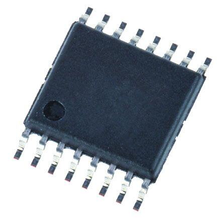
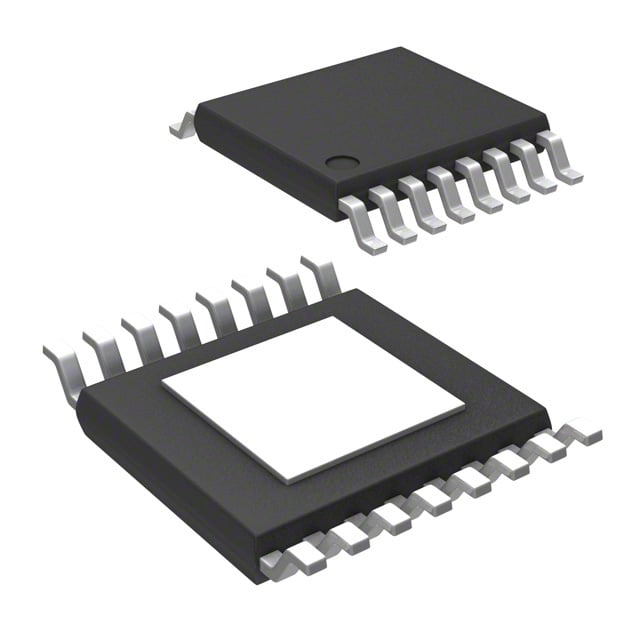
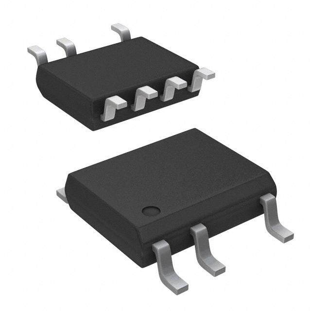
| 描述 | IC REG BUCK SYNC 1.8V 16HTSSOP稳压器—开关式稳压器 4.5 to 20V Inp 3-A Synch PWM Switch |
| 产品分类 | |
| 品牌 | Texas Instruments |
| 产品手册 | |
| 产品图片 |
|
| rohs | 符合RoHS无铅 / 符合限制有害物质指令(RoHS)规范要求 |
| 产品系列 | 电源管理 IC,稳压器—开关式稳压器,Texas Instruments TPS54354PWPSWIFT™ |
| 数据手册 | |
| 产品型号 | TPS54354PWP |
| PWM类型 | - |
| 产品培训模块 | http://www.digikey.cn/PTM/IndividualPTM.page?site=cn&lang=zhs&ptm=16804 |
| 产品目录页面 | |
| 产品种类 | 稳压器—开关式稳压器 |
| 供应商器件封装 | 16-HTSSOP |
| 其它名称 | 296-17071 |
| 制造商产品页 | http://www.ti.com/general/docs/suppproductinfo.tsp?distId=10&orderablePartNumber=TPS54354PWP |
| 包装 | 管件 |
| 单位重量 | 62.700 mg |
| 同步整流器 | 是 |
| 商标 | Texas Instruments |
| 安装类型 | 表面贴装 |
| 安装风格 | SMD/SMT |
| 宽度 | 4.4 mm |
| 封装 | Tube |
| 封装/外壳 | 16-TSSOP (0.173", 4.40mm 宽)裸焊盘 |
| 封装/箱体 | HTSSOP-16 |
| 工作温度 | -40°C ~ 85°C |
| 工作温度范围 | - 40 C to + 85 C |
| 工厂包装数量 | 90 |
| 开关频率 | 500 kHz |
| 拓扑结构 | Buck |
| 最大工作温度 | + 85 C |
| 最大输入电压 | 20 V |
| 最小工作温度 | - 40 C |
| 最小输入电压 | 4.5 V |
| 标准包装 | 90 |
| 电压-输入 | 4.5 V ~ 20 V |
| 电压-输出 | 1.8V |
| 电流-输出 | 3A |
| 类型 | 降压(降压) |
| 系列 | TPS54354 |
| 输入电压 | 4.5 V to 20 V |
| 输出数 | 1 |
| 输出电压 | 1.8 V |
| 输出电流 | 3 A |
| 输出端数量 | 1 Output |
| 输出类型 | 固定 |
| 频率-开关 | 250kHz,500kHz |


- 商务部:美国ITC正式对集成电路等产品启动337调查
- 曝三星4nm工艺存在良率问题 高通将骁龙8 Gen1或转产台积电
- 太阳诱电将投资9.5亿元在常州建新厂生产MLCC 预计2023年完工
- 英特尔发布欧洲新工厂建设计划 深化IDM 2.0 战略
- 台积电先进制程称霸业界 有大客户加持明年业绩稳了
- 达到5530亿美元!SIA预计今年全球半导体销售额将创下新高
- 英特尔拟将自动驾驶子公司Mobileye上市 估值或超500亿美元
- 三星加码芯片和SET,合并消费电子和移动部门,撤换高东真等 CEO
- 三星电子宣布重大人事变动 还合并消费电子和移动部门
- 海关总署:前11个月进口集成电路产品价值2.52万亿元 增长14.8%


PDF Datasheet 数据手册内容提取
(cid:1)(cid:2)(cid:3)(cid:4)(cid:5)(cid:6)(cid:4)(cid:7)(cid:8) (cid:1)(cid:2)(cid:3)(cid:4)(cid:5)(cid:6)(cid:4)(cid:6) (cid:1)(cid:2)(cid:3)(cid:4)(cid:5)(cid:6)(cid:4)(cid:5)(cid:8) (cid:1)(cid:2)(cid:3)(cid:4)(cid:5)(cid:6)(cid:4)(cid:4) (cid:9)(cid:8)(cid:5) !! (cid:1) (cid:4)(cid:8)(cid:15) !! (cid:1)(cid:2)(cid:3)(cid:4)(cid:5)(cid:6)(cid:4)(cid:9)(cid:8) (cid:1)(cid:2)(cid:3)(cid:4)(cid:5)(cid:6)(cid:4)(cid:10) www.ti.com SLVS519A − MAY 2004 − REVISED OCTOBER 2004 (cid:5)(cid:11)(cid:4)(cid:12)(cid:13) (cid:1)(cid:14) (cid:7)(cid:15)(cid:12)(cid:13) (cid:16)(cid:17)(cid:2)(cid:18)(cid:1)(cid:8) (cid:6)(cid:12)(cid:19) (cid:14)(cid:18)(cid:1)(cid:2)(cid:18)(cid:1) (cid:3)(cid:20)(cid:17)(cid:21)(cid:22)(cid:23)(cid:14)(cid:17)(cid:14)(cid:18)(cid:3) (cid:2)(cid:24)(cid:25) (cid:3)(cid:24)(cid:16)(cid:1)(cid:21)(cid:22)(cid:26)(cid:23) (cid:24)(cid:16)(cid:1)(cid:22) (cid:16)(cid:17)(cid:1)(cid:26)(cid:27)(cid:23)(cid:19)(cid:1)(cid:26)(cid:28) (cid:29)(cid:26)(cid:1) (cid:30)(cid:3)(cid:24)(cid:16)(cid:29)(cid:1)(cid:31) FEATURES DESCRIPTION (cid:1) 100 mΩ, 4.5-A Peak MOSFET Switch for High The TPS5435x is a medium output current synchronous Efficiency at 3-A Continuous Output Current buck PWM converter with an integrated high side (cid:1) Uses External Lowside MOSFET or Diode MOSFET and a gate driver for an optional low side (cid:1) Fixed Output Versions − external MOSFET. Features include a high performance 1.2V/1.5V/1.8V/2.5V/3.3V/5.0V voltage error amplifier that enables maximum (cid:1) performance under transient conditions. The TPS5435x Internally Compensated for Low Parts Count (cid:1) has an under-voltage-lockout circuit to prevent start-up Synchronizes to External Clock until the input voltage reaches a preset value; an internal (cid:1) 180(cid:2) Out of Phase Synchronization slow-start circuit to limit in-rush currents; and a power good (cid:1) Wide PWM Frequency − Fixed 250 kHz, output to indicate valid output conditions. The 500kHz or Adjustable 250 kHz to 700 kHz synchronization feature is configurable as either an input (cid:1) Internal Slow Start or an output for easy 180° out of phase synchronization. (cid:1) Load Protected by Peak Current Limit and The TPS5435x devices are available in a thermally Thermal Shutdown enhanced 16-pin TSSOP (PWP) PowerPAD package. (cid:1) Adjustable Undervoltage Lockout TI provides evaluation modules and the SWIFT Designer (cid:1) 16-Pin TSSOP PowerPAD(cid:3) Package software tool to aid in quickly achieving high-performance power supply designs to meet aggressive equipment APPLICATIONS development cycles. (cid:1) Industrial & Commercial Low Power Systems (cid:1) LCD Monitors and TVs EFFICIENCY (cid:1) vs Computer Peripherals OUTPUT CURRENT (cid:1) Point of Load Regulation for High 100 VI = 6 V Performance DSPs, FPGAs, ASICs and 95 VI = 12 V Microprocessors 90 % 85 − y 80 SIMPLIFIED SCHEMATIC c n cie 75 Effi 70 Input 65 Voltage TPS54356 60 VI= 12 V SYNC VIN 55 VO= 3.3 V PWRGD 50 fs = 500 kHz ENA 0 1 2 3 4 BOOT IO − Output Current − A BIAS PH Output LSG Voltage PGND VSENSE PWRPAD Please be aware that an important notice concerning availability, standard warranty, and use in critical applications of TexasInstruments semiconductor products and disclaimers thereto appears at the end of this data sheet. PowerPAD and SWIFT are trademarks of Texas Instruments. (cid:2)(cid:23)(cid:14)(cid:28)(cid:18)(cid:21)(cid:1)(cid:16)(cid:14)(cid:17) (cid:28)(cid:19)(cid:1)(cid:19) "#$%&!’("%# ") *+&&,#( ’) %$ -+./"*’("%# 0’(,(cid:11) (cid:2)&%0+*() Copyright 2004, Texas Instruments Incorporated *%#$%&! (% )-,*"$"*’("%#) -,& (1, (,&!) %$ (cid:1),2’) (cid:16)#)(&+!,#() )(’#0’&0 3’&&’#(4(cid:11) (cid:2)&%0+*("%# -&%*,))"#5 0%,) #%( #,*,))’&"/4 "#*/+0, (,)("#5 %$ ’// -’&’!,(,&)(cid:11)
(cid:1)(cid:2)(cid:3)(cid:4)(cid:5)(cid:6)(cid:4)(cid:7)(cid:8) (cid:1)(cid:2)(cid:3)(cid:4)(cid:5)(cid:6)(cid:4)(cid:6) (cid:1)(cid:2)(cid:3)(cid:4)(cid:5)(cid:6)(cid:4)(cid:5)(cid:8) (cid:1)(cid:2)(cid:3)(cid:4)(cid:5)(cid:6)(cid:4)(cid:4) (cid:1)(cid:2)(cid:3)(cid:4)(cid:5)(cid:6)(cid:4)(cid:9)(cid:8) (cid:1)(cid:2)(cid:3)(cid:4)(cid:5)(cid:6)(cid:4)(cid:10) www.ti.com SLVS519A − MAY 2004 − REVISED OCTOBER 2004 These devices have limited built-in ESD protection. The leads should be shorted together or the device placed in conductive foam during storage or handling to prevent electrostatic damage to the MOS gates. ORDERING INFORMATION TA OUTPUT VOLTAGE PACKAGE PART NUMBER 1.2 V Plastic HTSSOP (PWP) TPS54352PWP 1.5 V Plastic HTSSOP (PWP) TPS54353PWP 1.8 V Plastic HTSSOP (PWP) TPS54354PWP −−4400°°CC ttoo 8855°°CC 2.5 V Plastic HTSSOP (PWP) TPS54355PWP 3.3 V Plastic HTSSOP (PWP) TPS54356PWP 5.0 V Plastic HTSSOP (PWP) TPS54357PWP (1)The PWP package is also available taped and reeled. Add an R suffix to the device type (i.e. TPS5435xPWPR). PACKAGE DISSIPATION RATINGS(1) THERMAL IMPEDANCE TA = 25°C TA = 70°C TA = 85°C PACKAGE JUNCTION-TO-AMBIENT POWER RATING POWER RATING POWER RATING 16-Pin PWP with solder(2) 42.1°C/W 2.36 1.31 0.95 16-Pin PWP without solder 151.9°C/W 0.66 0.36 0.26 (1)See Figure 47 for power dissipation curves. (2)Test Board Conditions 1. Thickness: 0.062” 2. 3” x 3” 3. 2 oz. Copper traces located on the top and bottom of the PCB for soldering 4. Copper areas located on the top and bottom of the PCB for soldering 5. Power and ground planes, 1 oz. copper (0.036 mm thick) 6. Thermal vias, 0.33 mm diameter, 1.5 mm pitch 7. Thermal isolation of power plane For more information, refer to TI technical brief SLMA002. 2
(cid:1)(cid:2)(cid:3)(cid:4)(cid:5)(cid:6)(cid:4)(cid:7)(cid:8) (cid:1)(cid:2)(cid:3)(cid:4)(cid:5)(cid:6)(cid:4)(cid:6) (cid:1)(cid:2)(cid:3)(cid:4)(cid:5)(cid:6)(cid:4)(cid:5)(cid:8) (cid:1)(cid:2)(cid:3)(cid:4)(cid:5)(cid:6)(cid:4)(cid:4) (cid:1)(cid:2)(cid:3)(cid:4)(cid:5)(cid:6)(cid:4)(cid:9)(cid:8) (cid:1)(cid:2)(cid:3)(cid:4)(cid:5)(cid:6)(cid:4)(cid:10) www.ti.com SLVS519A − MAY 2004 − REVISED OCTOBER 2004 ABSOLUTE MAXIMUM RATINGS over operating free-air temperature range unless otherwise noted(1) UNIT VIN −0.3 V to 21.5 V VSENSE −0.3 V to 8.0 V UVLO −0.3 V to 8.0 V IInnppuutt vvoollttaaggee rraannggee,, VVII SYNC −0.3 V to 4.0 V ENA −0.3 V to 4.0 V BOOT VI(PH) + 8.0 V VBIAS −0.3 to 8.5 V LSG −0.3 to 8.5 V SYNC −0.3 to 4.0 V OOuuttppuutt vvoollttaaggee rraannggee,, VVOO RT −0.3 to 4.0 V PWRGD −0.3 to 6.0 V COMP −0.3 to 4.0 V PH −1.5 V to 22 V PH Internally Limited (A) SSoouurrccee ccuurrrreenntt,, IIOO LSG (Steady State Current) 10 mA COMP, VBIAS 3 mA SYNC 5 mA LSG (Steady State Current) 100 mA SSiinnkk ccuurrrreenntt,, IISS PH (Steady State Current) 500 mA COMP 3 mA ENA, PWRGD 10 mA Voltage differential AGND to PGND ±0.3 V Operating virtual junction temperature range, TJ −40°C to +150°C Storage temperature, Tstg −65°C to +150°C Lead temperature 1,6 mm (1/16 inch) from case for 10 seconds 260°C (1)Stresses beyond those listed under “absolute maximum ratings” may cause permanent damage to the device. These are stress ratings only, and functional operation of the device at these or any other conditions beyond those indicated under “recommended operating conditions” is not implied. Exposure to absolute-maximum-rated conditions for extended periods may affect device reliability. ELECTROSTATIC DISCHARGE (ESD) PROTECTION MIN MAX UNIT Human body model 600 V CDM 1.5 kV RECOMMENDED OPERATING CONDITIONS MIN NOM MAX UNIT TPS54352−6 4.5 20 IInnppuutt vvoollttaaggee rraannggee,, VVII VV TPS54357 6.65 20 Operating junction temperature, TJ −40 125 °C 3
(cid:1)(cid:2)(cid:3)(cid:4)(cid:5)(cid:6)(cid:4)(cid:7)(cid:8) (cid:1)(cid:2)(cid:3)(cid:4)(cid:5)(cid:6)(cid:4)(cid:6) (cid:1)(cid:2)(cid:3)(cid:4)(cid:5)(cid:6)(cid:4)(cid:5)(cid:8) (cid:1)(cid:2)(cid:3)(cid:4)(cid:5)(cid:6)(cid:4)(cid:4) (cid:1)(cid:2)(cid:3)(cid:4)(cid:5)(cid:6)(cid:4)(cid:9)(cid:8) (cid:1)(cid:2)(cid:3)(cid:4)(cid:5)(cid:6)(cid:4)(cid:10) www.ti.com SLVS519A − MAY 2004 − REVISED OCTOBER 2004 ELECTRICAL CHARACTERISTICS TJ = –40°C to 125°C, VIN = 4.5 V to 20 V (unless otherwise noted) PARAMETER TEST CONDITIONS MIN TYP MAX UNIT SUPPLY CURRENT Operating current, PH pin open, 5 mA IIQQ QQuuiieesscceenntt ccuurrrreenntt No external low side MOSFET, RT = Hi-Z Shutdown, ENA = 0 V 1 mA TPS54352−6 4.32 4.49 SSttaarrtt tthhrreesshhoolldd vvoollttaaggee VV TPS54357 6.4 6.65 TPS54352−6 3.69 3.97 VVIINN SSttoopp tthhrreesshhoolldd vvoollttaaggee VV TPS54357 5.45 5.80 TPS54352−6 350 mV HHyysstteerreessiiss TPS54357 600 mV OUTPUT VOLTAGE TJ = 25°C, IO = 100 mA to 3 A 1.88 1.2 1.212 TTPPSS5544335522 IO = 100 mA to 3 A 1.176 1.2 1.224 TJ = 25°C, IO = 100 mA to 3 A 1.485 1.5 1.515 TTPPSS5544335533 IO = 100 mA to 3 A 1.47 1.5 1.53 TJ = 25°C, IO = 100 mA to 3 A 1.782 1.8 1.818 TTPPSS5544335544 IO = 100 mA to 3 A 1.764 1.8 1.836 VVOO OOuuttppuutt vvoollttaaggee TJ = 25°C, IO = 100 mA to 3 A 2.475 2.5 2.525 VV TTPPSS5544335555 IO = 100 mA to 3 A 2.45 2.5 2.55 TJ = 25°C, VIN = 5.5 V to 20 V, IO = 100 mA to 3 A 3.267 3.3 3.333 TTPPSS5544335566 VIN = 5.5 V to 20 V, IO = 100 mA to 3 A 3.234 3.3 3.366 TJ = 25°C, VIN = 7.5 V to 20 V, IO = 100 mA to 3 A 4.95 5.0 5.05 TTPPSS5544335577 VIN = 7.5 V to 20 V, IO = 100 mA to 3 A 4.90 5.0 5.10 UNDER VOLTAGE LOCK OUT (UVLO PIN) Start threshold voltage 1.20 1.24 V UUVVLLOO Stop threshold voltage 1.02 1.10 V Hysteresis 100 mV BIAS VOLTAGE (VBIAS PIN) IVBIAS = 1 mA, VIN ≥ 12 V 7.5 7.8 8.0 VVBBIIAASS OOuuttppuutt vvoollttaaggee VV IVBIAS = 1 mA, VIN = 4.5 V 4.4 4.47 4.5 OSCILLATOR (RT PIN) RT Grounded 200 250 300 IInntteerrnnaallllyy sseett PPWWMM sswwiittcchhiinngg ffrreeqquueennccyy kkHHzz RT Open 400 500 600 Externally set PWM switching frequency RT = 100 kΩ (1% resistor to AGND) 425 500 575 kHz 4
(cid:1)(cid:2)(cid:3)(cid:4)(cid:5)(cid:6)(cid:4)(cid:7)(cid:8) (cid:1)(cid:2)(cid:3)(cid:4)(cid:5)(cid:6)(cid:4)(cid:6) (cid:1)(cid:2)(cid:3)(cid:4)(cid:5)(cid:6)(cid:4)(cid:5)(cid:8) (cid:1)(cid:2)(cid:3)(cid:4)(cid:5)(cid:6)(cid:4)(cid:4) (cid:1)(cid:2)(cid:3)(cid:4)(cid:5)(cid:6)(cid:4)(cid:9)(cid:8) (cid:1)(cid:2)(cid:3)(cid:4)(cid:5)(cid:6)(cid:4)(cid:10) www.ti.com SLVS519A − MAY 2004 − REVISED OCTOBER 2004 ELECTRICAL CHARACTERISTICS (CONTINUED) TJ = –40°C to 125°C, VIN = 4.5 V to 20 V (unless otherwise noted) PARAMETER TEST CONDITIONS MIN TYP MAX UNIT FALLING EDGE TRIGGERED BIDIRECTIONAL SYNC SYSTEM (SYNC PIN) SYNC out low-to-high rise time (10%/90%) (1) 25 pF to ground 200 500 ns SYNC out high-to-low fall time (90%/10%) (1) 25 pF to ground 5 10 ns Delay from rising edge to rising edge of PH Falling edge delay time (1) 180 ° pins, see Figure 19 Minimum input pulse width (1) RT = 100 kΩ 100 ns Delay (falling edge SYNC to rising edge PH) (1) RT = 100 kΩ 360 ns SYNC out high level voltage 50-kΩ Resistor to ground, no pullup resistor 2.5 V SYNC out low level voltage 0.6 V SYNC in low level threshold 0.8 V SYNC in high level threshold 2.3 V Percentage of programmed frequency −10% 10% SSYYNNCC iinn ffrreeqquueennccyy rraannggee ((11)) 225 770 kHz FEED− FORWARD MODULATOR (INTERNAL SIGNAL) Modulator gain VIN = 12 V, TJ = 25°C 8 V/V Modulator gain variation −25% 25% Minimum controllable ON time (1) 180 ns Maximum duty factor (1) VIN = 4.5 V 80% 86% VSENSE PIN Input bias current, VSENSE pin 1 µA ENABLE (ENA PIN) Disable low level input voltage 0.5 V fs = 250 kHz, RT = ground (1) 3.20 TTPPSS5544335522 fs = 500 kHz, RT = Hi−Z (1) 1.60 fs = 250 kHz, RT = ground (1) 4.00 TTPPSS5544335533 fs = 500 kHz, RT = Hi−Z (1) 2.00 fs = 250 kHz, RT = ground (1) 4.60 TTPPSS5544335544 IInntteerrnnaall ssllooww--ssttaarrtt ttiimmee fs = 500 kHz, RT = Hi−Z (1) 2.30 mmss ((1100%% ttoo 9900%%)) fs = 250 kHz, RT = ground (1) 4.40 TTPPSS5544335555 fs = 500 kHz, RT = Hi−Z (1) 2.20 fs = 250 kHz, RT = ground (1) 5.90 TTPPSS5544335566 fs = 500 kHz, RT = Hi−Z (1) 2.90 fs = 250 kHz, RT = ground (1) 5.40 TTPPSS5544335577 fs = 500 kHz, RT = Hi−Z (1) 2.70 Pullup current source 1.8 5 10 µA Pulldown MOSFET II(ENA)= 1 mA 0.1 V POWER GOOD (PWRGD PIN) Power good threshold Rising voltage 97% fs = 250 kHz 4 RRiissiinngg eeddggee ddeellaayy ((11)) mmss fs = 500 kHz 2 Output saturation voltage Isink = 1 mA, VIN > 4.5 V 0.05 V PPWWRRGGDD Output saturation voltage Isink = 100 µA, VIN = 0 V 0.76 V Open drain leakage current Voltage on PWRGD = 6 V 3 µA (1)Ensured by design, not production tested. 5
(cid:1)(cid:2)(cid:3)(cid:4)(cid:5)(cid:6)(cid:4)(cid:7)(cid:8) (cid:1)(cid:2)(cid:3)(cid:4)(cid:5)(cid:6)(cid:4)(cid:6) (cid:1)(cid:2)(cid:3)(cid:4)(cid:5)(cid:6)(cid:4)(cid:5)(cid:8) (cid:1)(cid:2)(cid:3)(cid:4)(cid:5)(cid:6)(cid:4)(cid:4) (cid:1)(cid:2)(cid:3)(cid:4)(cid:5)(cid:6)(cid:4)(cid:9)(cid:8) (cid:1)(cid:2)(cid:3)(cid:4)(cid:5)(cid:6)(cid:4)(cid:10) www.ti.com SLVS519A − MAY 2004 − REVISED OCTOBER 2004 ELECTRICAL CHARACTERISTICS (CONTINUED) TJ = –40°C to 125°C, VIN = 4.5 V to 20 V (unless otherwise noted) PARAMETER TEST CONDITIONS MIN TYP MAX UNIT CURRENT LIMIT Current limit VIN = 12 V 3.3 4.5 6.5 A Current limit hiccup time (1) fs = 500 kHz 4.5 ms THERMAL SHUTDOWN Thermal shutdown trip point (1) 165 (cid:2)C Thermal shutdown hysteresis (1) 7 (cid:2)C LOW SIDE MOSFET DRIVER (LSG PIN) Turn on rise time, (10%/90%) (1) VIN = 4.5 V, Capacitive load = 1000 pF 15 ns Deadtime (1) VIN = 12 V 60 ns VIN = 4.5 V sink/source 7.5 DDrriivveerr OONN rreessiissttaannccee ΩΩ VIN = 12 V sink/source 5 OUTPUT POWER MOSFETS (PH PIN) Phase node voltage when disabled DC conditions and no load, ENA = 0 V 0.5 V VIN = 4.5 V, Idc = 100 mA 1.13 1.42 VVoollttaaggee ddrroopp,, llooww ssiiddee FFEETT aanndd ddiiooddee VV VIN = 12 V, Idc = 100 mA 1.08 1.38 VIN = 4.5 V, BOOT−PH = 4.5 V, IO = 0.5 A 150 300 rrDDSS((OONN)) HHiigghh ssiiddee ppoowweerr MMOOSSFFEETT sswwiittcchh ((22)) mmΩΩ VIN = 12 V, BOOT−PH = 8 V, IO = 0.5 A 100 200 (1)Ensured by design, not production tested. (2)Resistance from VIN to PH pins. 6
(cid:1)(cid:2)(cid:3)(cid:4)(cid:5)(cid:6)(cid:4)(cid:7)(cid:8) (cid:1)(cid:2)(cid:3)(cid:4)(cid:5)(cid:6)(cid:4)(cid:6) (cid:1)(cid:2)(cid:3)(cid:4)(cid:5)(cid:6)(cid:4)(cid:5)(cid:8) (cid:1)(cid:2)(cid:3)(cid:4)(cid:5)(cid:6)(cid:4)(cid:4) (cid:1)(cid:2)(cid:3)(cid:4)(cid:5)(cid:6)(cid:4)(cid:9)(cid:8) (cid:1)(cid:2)(cid:3)(cid:4)(cid:5)(cid:6)(cid:4)(cid:10) www.ti.com SLVS519A − MAY 2004 − REVISED OCTOBER 2004 PIN ASSIGNMENTS PWP PACKAGE (TOP VIEW) VIN 1 16 BOOT VIN 2 15 PH UVLO 3 14 PH PWRGD 4 THERMAL 13 LSG RT 5 PAD 12 VBIAS SYNC 6 11 PGND ENA 7 10 AGND COMP 8 9 VSENSE NOTE: If there is not a Pin 1 indicator, turn device to enable reading the symbol from left to right. Pin 1 is at the lower left corner of the device. Terminal Functions TERMINAL DDEESSCCRRIIPPTTIIOONN NO. NAME 1, 2 VIN Input supply voltage, 4.5 V to 20 V. Must bypass with a low ESR 10-µF ceramic capacitor. Place cap as close to device as possible; see Figure 23 for an example. 3 UVLO Undervoltage lockout pin. Connecting an external resistive voltage divider from VIN to the pin will override the internal default VIN start and stop thresholds. 4 PWRGD Power good output. Open drain output. A low on the pin indicates that the output is less than the desired output voltage. There is an internal rising edge filter on the output of the PWRGD comparator. 5 RT Frequency setting pin. Connect a resistor from RT to AGND to set the switching frequency. Connecting the RT pin to ground or floating will set the frequency to an internally preselected frequency. 6 SYNC Bidirectional synchronization I/O pin. SYNC pin is an output when the RT pin is floating or connected low. The output is a falling edge signal out of phase with the rising edge of PH. SYNC may be used as an input to synchronize to a system clock by connecting to a falling edge signal when an RT resistor is used. See 180° Out of Phase Synchronization operation in the Application Information section. In ALL cases, a 10 kΩ resistor Must be tied to the SYNC pin in parallel with ground. For information on how to extend slow start, see the Enable (ENA) and Internal Slow Start section on page 9. 7 ENA Enable. Below 0.5 V, the device stops switching. Float pin to enable. 8 COMP Error amplifier output. Do NOT connect ANYTHING to this pin. 9 VSENSE Feedback pin 10 AGND Analog ground—internally connected to the sensitive analog ground circuitry. Connect to PGND and PowerPAD. 11 PGND Power ground—Noisy internal ground—Return currents from the LSG driver output return through the PGND pin. Connect to AGND and PowerPAD. 12 VBIAS Internal 8.0-V bias voltage. A 1.0-µF ceramic bypass capacitance is required on the VBIAS pin. 13 LSG Gate drive for optional low side MOSFET. Connect gate of n-channel MOSFET for a higher efficiency synchronous buck converter configuration. Otherwise, leave open and connect schottky diode from ground to PH pins. 14, 15 PH Phase node—Connect to external L−C filter. 16 BOOT Bootstrap capacitor for high side gate driver. Connect a 0.1-µF ceramic capacitor from BOOT to PH pins. PowerPAD PGND and AGND pins must be connected to the exposed pad for proper operation. See Figure 23 for an example PCB layout. 7
(cid:1)(cid:2)(cid:3)(cid:4)(cid:5)(cid:6)(cid:4)(cid:7)(cid:8) (cid:1)(cid:2)(cid:3)(cid:4)(cid:5)(cid:6)(cid:4)(cid:6) (cid:1)(cid:2)(cid:3)(cid:4)(cid:5)(cid:6)(cid:4)(cid:5)(cid:8) (cid:1)(cid:2)(cid:3)(cid:4)(cid:5)(cid:6)(cid:4)(cid:4) (cid:1)(cid:2)(cid:3)(cid:4)(cid:5)(cid:6)(cid:4)(cid:9)(cid:8) (cid:1)(cid:2)(cid:3)(cid:4)(cid:5)(cid:6)(cid:4)(cid:10) www.ti.com SLVS519A − MAY 2004 − REVISED OCTOBER 2004 FUNCTIONAL BLOCK DIAGRAM BOOT VIN PH 320 kΩ Hiccup UVLO UVLO Current Limit 125 kΩ(1) 1.2V SYNC 2x Oscillator RT Bias + Drive PWM Ramp Regulator VBIAS (FeedFoward) Z3 PWM S Q Adaptive Deadtime VBIAS COMP Comparator and Z1 Control Logic VSENSE Z4 R LSG Z2 Error VBIAS2 Amplifier Z5 Thermal Reference Shutdown System PWRGD 5 µA UVLO VSENSE Rising Edge 97% Ref UVLO ENA Delay Hiccup Hiccup Timer TPS5435X (1) 75 kΩ for the TPS54357 POWERPAD VBIAS PGND AGND DETAILED DESCRIPTION Undervoltage Lockout (UVLO) The undervoltage lockout (UVLO) system has an internal accurate, but the absolute values of the internal resistors voltage divider from VIN to AGND. The defaults for the may vary as much as 15%. If high accuracy is required for start/stop values are labeled VIN and given in Table 1. The an externally adjusted UVLO threshold, select lower value internal UVLO threshold can be overridden by placing an external resistors to set the UVLO threshold. Using a 1-kΩ external resistor divider from VIN to ground. The internal resistor for the low side resistor (R2 see Figure 1) is divider values are approximately 320 kΩ for the high side recommended. Under no circumstances should the UVLO resistor and 125 kΩ for the low side resistor. The divider pin be connected directly to VIN. ratio (and therefore the default start/stop values) is quite Table 1. Start/Stop Voltage Threshold START VOLTAGE THRESHOLD STOP VOLTAGE THRESHOLD TPS54352−6 4.49 3.69 VVIINN ((DDeeffaauulltt)) TPS54357 6.65 5.45 UVLO 1.24 1.02 The equations for selecting the UVLO resistors are: (R1 (cid:4) 1k(cid:1)) (cid:2) 1.02V VIN(stop) (cid:1) VIN(start) (cid:2) 1k(cid:1) 1k(cid:1) (2) R1 (cid:1) (cid:3)1k(cid:1) 1.24V (1) 8
(cid:1)(cid:2)(cid:3)(cid:4)(cid:5)(cid:6)(cid:4)(cid:7)(cid:8) (cid:1)(cid:2)(cid:3)(cid:4)(cid:5)(cid:6)(cid:4)(cid:6) (cid:1)(cid:2)(cid:3)(cid:4)(cid:5)(cid:6)(cid:4)(cid:5)(cid:8) (cid:1)(cid:2)(cid:3)(cid:4)(cid:5)(cid:6)(cid:4)(cid:4) (cid:1)(cid:2)(cid:3)(cid:4)(cid:5)(cid:6)(cid:4)(cid:9)(cid:8) (cid:1)(cid:2)(cid:3)(cid:4)(cid:5)(cid:6)(cid:4)(cid:10) www.ti.com SLVS519A − MAY 2004 − REVISED OCTOBER 2004 Input Voltage Supply 320 kΩ R1 R2 1 kΩ 125 kΩ (1) 5 µA Disabled RSS (1) 75 kΩ for the TPS54357 C SS Enabled Figure 1. Circuit Using External UVLO Function Figure 2. Interfacing to the ENA Pin For applications which require an undervoltage lock out Extending Slow Start Time (UVLO) threshold greater than 4.49 V (6.6 V for In applications that use large values of output capacitance TPS54357), external resistors may be implemented, see there may be a need to extend the slow start time to Figure 1, to adjust the start voltage threshold. For example, prevent the startup current from tripping the current limit. an application needing an UVLO start voltage of The current limit circuit is designed to disable the high side approximately 7.8 V using the equation (1), R1 is MOSFET and reset the internal voltage reference for a calculated to the nearest standard resistor value of short amount of time when the high side MOSFET current 5.36 kΩ. Using equation (2), the input voltage stop exceeds the current limit threshold. If the output threshold is calculated as 6.48 V. capacitance and load current cause the startup current to exceed the current limit threshold, the power supply output Enable (ENA) and Internal Slow Start will not reach the desired output voltage. To extend the slow start time and to reduce the startup current, an The TPS5435x has an internal digital slow start that ramps external resistor and capacitor can be added to the ENA the reference voltage to its final value in 1150 switching pin. The slow start capacitance is calculated using the cycles. The internal slow start time (10% − 90%) is following equation: approximated by the following expression: C (µF) = 5.55 (cid:2) 10−3 (cid:2) n (cid:2) T (ms) SS ss T (ms)(cid:1) 1.15k (4) SS_INTERNAL ƒ (kHz)(cid:2)n Use n in Table 2 s (3) Use n in Table 2 The R resistor must be 2 kΩ and the slow start capacitor SS must be less than 0.47 µF. Switching Frequency (RT) Table 2. Slow Start Characteristics The TPS5435x has an internal oscillator that operates at twice the PWM switching frequency. The internal oscillator frequency is controlled by the RT pin. Grounding the RT DEVICE n pin sets the PWM switching frequency to a default TPS54352 1.485 frequency of 250 kHz. Floating the RT pin sets the PWM TPS54353 1.2 switching frequency to 500 kHz. TPS54354 1 Connecting a resistor from RT to AGND sets the frequency TPS54355 1.084 according to the following equation (also see Figure 30). TPS54356 0.818 RT(k(cid:1))(cid:1) 46000 TPS54357 0.900 ƒ (kHz)(cid:3)35.9 s (5) The RT pin controls the SYNC pin functions. If the RT pin Once the TPS5435x device is in normal regulation, the is floating or grounded, SYNC is an output. If the switching ENA pin is high. If the ENA pin is pulled below the stop frequency has been programmed using a resistor from RT threshold of 0.5 V, switching stops and the internal slow to AGND, then SYNC functions as an input. start resets. If an application requires the TPS5435x to be disabled, use open drain or open collector output logic to The internal voltage ramp charging current increases interface to the ENA pin (see Figure 2). The ENA pin has linearly with the set frequency and keeps the feed forward an internal pullup current source. Do not use external modulator constant (Km = 8) regardless of the frequency pullup resistors. set point. 9
(cid:1)(cid:2)(cid:3)(cid:4)(cid:5)(cid:6)(cid:4)(cid:7)(cid:8) (cid:1)(cid:2)(cid:3)(cid:4)(cid:5)(cid:6)(cid:4)(cid:6) (cid:1)(cid:2)(cid:3)(cid:4)(cid:5)(cid:6)(cid:4)(cid:5)(cid:8) (cid:1)(cid:2)(cid:3)(cid:4)(cid:5)(cid:6)(cid:4)(cid:4) (cid:1)(cid:2)(cid:3)(cid:4)(cid:5)(cid:6)(cid:4)(cid:9)(cid:8) (cid:1)(cid:2)(cid:3)(cid:4)(cid:5)(cid:6)(cid:4)(cid:10) www.ti.com SLVS519A − MAY 2004 − REVISED OCTOBER 2004 Table 3. SWITCHING FREQUENCY SYNC PIN RT PIN 250 kHz, internally set Generates SYNC output signal AGND 500 kHz, internally set Generates SYNC output signal Float Terminate to quiet ground Externally set to 250 kHz to 700 kHz R = 215 kΩ to 69 kΩ with 10-kΩ resistor. Set RT resistor equal to 90% to 110% of external synchronization frequency.When using a dual setup (see Figure 27 for example), if the master 35x device RT pin is left floating, use a 110 kΩ Externally synchronized frequency Synchronization Signal resistor to tie the slave RT pin to ground. Conversely, if the master 35x device RT pin is grounded, use a 237 kΩ resistor to tie the slave RT pin to ground. 180(cid:2) Out of Phase Synchronization (SYNC) The SYNC pin is configurable as an input or as an output, When operating the two TPS5435x devices 180° out of per the description in the previous section. When phase, the total RMS input current is reduced. Thus operating as an input, the SYNC pin is a falling-edge reducing the amount of input capacitance needed and triggered signal (see Figures 3, 4, and 19). When operating increasing efficiency. as an output, the signal’s falling edge is approximately 180° out of phase with the rising edge of the PH pins. Thus, When synchronizing a TPS5435x to an external signal, the two TPS5435x devices operating in a system can share an timing resistor on the RT pin must be set so that the input capacitor and draw ripple current at twice the oscillator is programmed to run at 90% to 110% of the frequency of a single unit. synchronization frequency. VI(SYNC) VO(PH) Figure 3. SYNC Input Waveform 10
(cid:1)(cid:2)(cid:3)(cid:4)(cid:5)(cid:6)(cid:4)(cid:7)(cid:8) (cid:1)(cid:2)(cid:3)(cid:4)(cid:5)(cid:6)(cid:4)(cid:6) (cid:1)(cid:2)(cid:3)(cid:4)(cid:5)(cid:6)(cid:4)(cid:5)(cid:8) (cid:1)(cid:2)(cid:3)(cid:4)(cid:5)(cid:6)(cid:4)(cid:4) (cid:1)(cid:2)(cid:3)(cid:4)(cid:5)(cid:6)(cid:4)(cid:9)(cid:8) (cid:1)(cid:2)(cid:3)(cid:4)(cid:5)(cid:6)(cid:4)(cid:10) www.ti.com SLVS519A − MAY 2004 − REVISED OCTOBER 2004 Internal Oscillator VO(PH) VO(SYNC) Figure 4. SYNC Output Waveform Power Good (PWRGD) capacitor value of 1.0 µF. X7R or X5R grade dielectric ceramic capacitors are recommended because of their The VSENSE pin is compared to an internal reference stable characteristics over temperature. signal, if the VSENSE is greater than 97% and no other faults are present, the PWRGD pin presents a high Bootstrap Voltage (BOOT) impedance. A low on the PWRGD pin indicates a fault. The The BOOT capacitor obtains its charge cycle by cycle from PWRGD pin has been designed to provide a weak the VBIAS capacitor. A capacitor from the BOOT pin to the pull-down and indicates a fault even when the device is PH pins is required for operation. The bootstrap unpowered. If the TPS5435x has power and has any fault connection for the high side driver must have a bypass flag set, the TPS5435x indicates the power is not good by capacitor of 0.1 µF. driving the PWRGD pin low. The following events, singly or in combination, indicate power is not good: Error Amplifier (cid:1) The VSENSE pin is the error amplifier inverting input. The VSENSE pin out of bounds (cid:1) error amplifier is a true voltage amplifier with 1.5 mA of Overcurrent (cid:1) drive capability with a minimum of 60 dB of open loop Thermal shutdown (cid:1) voltage gain and a unity gain bandwidth of 2 MHz. UVLO undervoltage (cid:1) Input voltage not present (weak pull-down) Voltage Reference (cid:1) Slow-starting (cid:1) The voltage reference system produces a precision VBIAS voltage is low reference signal by scaling the output of a temperature stable bandgap circuit. During production testing, the Once the PWRGD pin presents a high impedance (i.e., bandgap and scaling circuits are trimmed to produce power is good), a VSENSE pin out of bounds condition 0.891V at the output of the error amplifier, with the forces PWRGD pin low (i.e., power is bad) after a time amplifier connected as a voltage follower. The trim delay. This time delay is a function of the switching procedure improves the regulation, since it cancels offset frequency and is calculated using equation 6: errors in the scaling and error amplifier circuits. T (cid:1) 1000 ms PWM Control and Feed Forward delay ƒ (kHz) s (6) Signals from the error amplifier output, oscillator, and current limit circuit are processed by the PWM control Bias Voltage (VBIAS) logic. Referring to the internal block diagram, the control logic includes the PWM comparator, PWM latch, and the The VBIAS regulator provides a stable supply for the adaptive dead-time control logic. During steady-state internal analog circuits and the low side gate driver. Up to operation below the current limit threshold, the PWM 1 mA of current can be drawn for use in an external comparator output and oscillator pulse train alternately application circuit. The VBIAS pin must have a bypass reset and set the PWM latch. 11
(cid:1)(cid:2)(cid:3)(cid:4)(cid:5)(cid:6)(cid:4)(cid:7)(cid:8) (cid:1)(cid:2)(cid:3)(cid:4)(cid:5)(cid:6)(cid:4)(cid:6) (cid:1)(cid:2)(cid:3)(cid:4)(cid:5)(cid:6)(cid:4)(cid:5)(cid:8) (cid:1)(cid:2)(cid:3)(cid:4)(cid:5)(cid:6)(cid:4)(cid:4) (cid:1)(cid:2)(cid:3)(cid:4)(cid:5)(cid:6)(cid:4)(cid:9)(cid:8) (cid:1)(cid:2)(cid:3)(cid:4)(cid:5)(cid:6)(cid:4)(cid:10) www.ti.com SLVS519A − MAY 2004 − REVISED OCTOBER 2004 Once the PWM latch is reset, the low-side driver and Low Side Gate Driver (LSG) integrated pull-down MOSFET remain on for a minimum LSG is the output of the low-side gate driver. The 100-mA duration set by the oscillator pulse width. During this period, the PWM ramp discharges rapidly to the valley MOSFET driver is capable of providing gate drive for most voltage. When the ramp begins to charge back up, the popular MOSFETs suitable for this application. Use the SWIFT Designer Software Tool to find the most low-side driver turns off and the high-side FET turns on. appropriate MOSFET for the application. Connect the LSG The peak PWM ramp voltage varies inversely with input pin directly to the gate of the low-side MOSFET. Do not use voltage to maintain a constant modulator and power stage a gate resistor as the resulting turn-on time may be too gain of 8 V/V. slow. As the PWM ramp voltage exceeds the error amplifier Integrated Pulldown MOSFET output voltage, the PWM comparator resets the latch, thus turning off the high-side FET and turning on the low-side The TPS5435x has a diode-MOSFET pair from PH to FET. The low-side driver remains on until the next PGND. The integrated MOSFET is designed for light−load oscillator pulse discharges the PWM ramp. continuous-conduction mode operation when only an external Schottky diode is used. The combination of devices keeps the inductor current continuous under During transient conditions, the error amplifier output can conditions where the load current drops below the be below the PWM ramp valley voltage or above the PWM inductor’s critical current. Care should be taken in the peak voltage. If the error amplifier is high, the PWM latch selection of inductor in applications using only a low-side is never reset and the high-side FET remains on until the Schottky diode. Since the inductor ripple current flows oscillator pulse signals the control logic to turn the through the integrated low-side MOSFET at light loads, the high-side FET off and the internal low-side FET and driver inductance value should be selected to limit the peak on. The device operates at its maximum duty cycle until the current to less than 0.3 A during the high-side FET turn off output voltage rises to the regulation set point, setting time. The minimum value of inductance is calculated using VSENSE to approximately the same voltage as the the following equation: internal voltage reference. If the error amplifier output is (cid:5) (cid:6) low, the PWM latch is continually reset and the high-side VO(cid:2) 1(cid:3)VO FET does not turn on. The internal low-side FET and low VI L(H)(cid:1) side driver remain on until the VSENSE voltage decreases ƒ (cid:2)0.6 s (7) to a range that allows the PWM comparator to change states. The TPS5435x is capable of sinking current Thermal Shutdown through the external low side FET until the output voltage reaches the regulation set point. The device uses the thermal shutdown to turn off the MOSFET drivers and controller if the junction temperature The minimum on time is designed to be 180 ns. During the exceeds 165°C. The device is restarted automatically internal slow-start interval, the internal reference ramps when the junction temperature decreases to 7°C below the from 0 V to 0.891 V. During the initial slow-start interval, the thermal shutdown trip point and starts up under control of internal reference voltage is very small resulting in a the slow-start circuit. couple of skipped pulses because the minimum on time Overcurrent Protection causes the actual output voltage to be slightly greater than the preset output voltage until the internal reference ramps Overcurrent protection is implemented by sensing the up. drain-to-source voltage across the high-side MOSFET and compared to a voltage level which represents the overcurrent threshold limit. If the drain-to-source voltage Deadtime Control exceeds the overcurrent threshold limit for more than 100ns, the ENA pin is pulled low, the high-side MOSFET is disabled, and the internal digital slow-start is reset to 0V. Adaptive dead time control prevents shoot through current ENA is held low for approximately the time that is from flowing in the integrated high-side MOSFET and the calculated by the following equation: external low-side MOSFET during the switching transitions by actively controlling the turn on times of the T (ms)(cid:1) 2250 drivers. The high-side driver does not turn on until the HICCUP ƒs(kHz) (8) voltage at the gate of the low-side MOSFET is below 1 V. The low-side driver does not turn on until the voltage at the Once the hiccup time is complete, the ENA pin is released gate of the high-side MOSFET is below 1 V. and the converter initiates the internal slow-start. 12
(cid:1)(cid:2)(cid:3)(cid:4)(cid:5)(cid:6)(cid:4)(cid:7)(cid:8) (cid:1)(cid:2)(cid:3)(cid:4)(cid:5)(cid:6)(cid:4)(cid:6) (cid:1)(cid:2)(cid:3)(cid:4)(cid:5)(cid:6)(cid:4)(cid:5)(cid:8) (cid:1)(cid:2)(cid:3)(cid:4)(cid:5)(cid:6)(cid:4)(cid:4) (cid:1)(cid:2)(cid:3)(cid:4)(cid:5)(cid:6)(cid:4)(cid:9)(cid:8) (cid:1)(cid:2)(cid:3)(cid:4)(cid:5)(cid:6)(cid:4)(cid:10) www.ti.com SLVS519A − MAY 2004 − REVISED OCTOBER 2004 Switching Frequency Limitations of curves is valid for output currents greater than 0.5 A. As Due to the internal design of the TPS54352−6 there are output currents decrease towards no load (0 A), the limitations to the maximum usable switching frequency for apparent on time increases, decreasing the maximum any given input voltage. This limit is constrained by the switching frequency that may be obtained for a given input minimum controllable on time which may be as high as and output voltage. Figure 32 shows the maximum 220 ns. Figure 31 shows the maximum switching switching frequency versus input voltage for each device frequency versus input voltage for each device. This family for zero load current various operating frequencies. 13
(cid:1)(cid:2)(cid:3)(cid:4)(cid:5)(cid:6)(cid:4)(cid:7)(cid:8) (cid:1)(cid:2)(cid:3)(cid:4)(cid:5)(cid:6)(cid:4)(cid:6) (cid:1)(cid:2)(cid:3)(cid:4)(cid:5)(cid:6)(cid:4)(cid:5)(cid:8) (cid:1)(cid:2)(cid:3)(cid:4)(cid:5)(cid:6)(cid:4)(cid:4) (cid:1)(cid:2)(cid:3)(cid:4)(cid:5)(cid:6)(cid:4)(cid:9)(cid:8) (cid:1)(cid:2)(cid:3)(cid:4)(cid:5)(cid:6)(cid:4)(cid:10) www.ti.com SLVS519A − MAY 2004 − REVISED OCTOBER 2004 TYPICAL CHARACTERISTICS Conditions are V = 12 V, V = 3.3 V, f = 500 kHz, I = 3 A, T = 25 °C, unless otherwise noted I O s O A MEASURED LOOP RESPONSE LOAD REGULATION LINE REGULATION 60 180 0.3 0.1 50 150 0.08 G − Gain − dB−−−123432100000000 Gain Phase −−−0369100029630000Phase − Degrees Output Voltage Change − % −000...1201 VVII == 1182 VV VI = 6 V Output Voltage Change − % −−−000000......0000002460642 IO = 3 AIO =I O0 A= 1.5 A −40 −120 −0.2 See Figure 25 −50 See Figure 25 −150 See Figure 25 −0.08 −60 −180 −0.3 −0.1 100 1 k 10 k 100 k 1 M 0 0.5 1 1.5 2 2.5 3 3.5 4 6 8 10 12 14 16 18 20 22 f − Frequency − Hz IO − Output Current − A VI − Input Voltage − V Figure 5 Figure 6 Figure 7 EFFICIENCY vs OUTPUT CURRENT INPUT RIPPLE VOLTAGE OUTPUT RIPPLE VOLTAGE 100 VI = 6 V 95 VI = 12 V VI(RIPPLE) = 100 mV/div (ac coupled) 90 VO(RIPPLE) = 10 mV/div (ac coupled) % 85 − Efficiency 778050 VI = 18 V Amplitude V(PH) = 5 V/div Amplitude V(PH) = 5 V/div 65 60 55 50 See Figure 25 See Figure 25 See Figure 25 0 1 2 3 4 Time − 1 µs/div Time − 1 µs/div IO − Output Current − A Figure 8 Figure 9 Figure 10 LOAD TRANSIENT RESPONSE POWER UP GATE DRIVE VOLTAGE VO = 50 mV/div (ac coupled) V(LSG) = 5 V/div mV e − mV VI = 5 V/div ons e − p s s n e e o d R p mplitu V(PH) = 5 V/div sient I(PH) = 1 A/div p Res VO= 2 V/div A Tran er U oad Pow V(PWRGD)= 2 V/div L See Figure 25 See Figure 25 See Figure 25 Time − 1 µs/div Time − 200 µs/div Time − 2 ms/div Figure 11 Figure 12 Figure 13 14
(cid:1)(cid:2)(cid:3)(cid:4)(cid:5)(cid:6)(cid:4)(cid:7)(cid:8) (cid:1)(cid:2)(cid:3)(cid:4)(cid:5)(cid:6)(cid:4)(cid:6) (cid:1)(cid:2)(cid:3)(cid:4)(cid:5)(cid:6)(cid:4)(cid:5)(cid:8) (cid:1)(cid:2)(cid:3)(cid:4)(cid:5)(cid:6)(cid:4)(cid:4) (cid:1)(cid:2)(cid:3)(cid:4)(cid:5)(cid:6)(cid:4)(cid:9)(cid:8) (cid:1)(cid:2)(cid:3)(cid:4)(cid:5)(cid:6)(cid:4)(cid:10) www.ti.com SLVS519A − MAY 2004 − REVISED OCTOBER 2004 Conditions are V = 12 V, V = 3.3 V, f = 500 kHz, I = 3 A, T = 25 °C, unless otherwise noted I O s O A EFFICIENCY vs OUTPUT CURRENT CONTINUOUS CONDUCTION MODE POWER DOWN 100 VI = 6 V V(PH) = 5 V/div 95 VI = 12 V e V 90 od ms − VI = 5 V/div % 85 on M Power Down Wavefor V(PVWOR=G 2D V)=/d 2iv V/div Efficiency − 6677805050 VI = 18 V Continuous Conducti I(L1) = 200 mA/div 55 See Figure 26 See Figure 26 See Figure 25 50 0 1 2 3 4 Time − 1 µs/div Time − 2 ms/div IO − Output Current − A Figure 14 Figure 15 Figure 16 LIGHT LOAD CONDUCTION SEQUENCING WAVEFORMS INPUT RIPPLE CANCELLATION V(PH) = 5 V/div V(PH1) = 10 V/div VI = 10 V/div V ction eforms − V VO1(3.3)= 2 V/div cellation − V(PH2) = 10 V/div u v n nd Wa Ca Light Load Co I(L1) = 200 mA/div Sequencing V(PWRGD1)= 2 V/div Input Ripple VI = 50 mV/div (ac coupled) VO2 (1.8)= 2 V/div See Figure 26 See Figure 27 See Figure 27 Time − 1 µs/div Time − 2 ms/div Time − 1 µs/div Figure 17 Figure 18 Figure 19 MEASURED LOOP RESPONSE MEASURED LOOP RESPONSE MEASURED LOOP RESPONSE 100 (cid:1)F POSCAP 2 x 180 (cid:1)F SP CAPACITORS 330 (cid:1)F OSCON 60 180 60 180 60 180 50 Phase 150 50 Phase 150 50 Phase 150 40 120 40 120 40 120 G − Gain − dB−−12321000000 Gain −−03690006300Phase − Degrees G − Gain − dB−−12321000000 Gain −−03690006300Phase − Degrees G − Gain − dB−−12321000000 Gain −−03690006300Phase − Degrees −30 −90 −30 −90 −30 −90 −40 −120 −40 −120 −40 −120 See Figure 28 See Figure 29 See Figure 30 −50 −150 −50 −150 −50 −150 −60 −180 −60 −180 −60 −180 100 1 k 10 k 100 k 1 M 100 1 k 10 k 100 k 1 M 100 1 k 10 k 100 k 1 M f − Frequency − Hz f − Frequency − Hz f − Frequency − Hz Figure 20 Figure 21 Figure 22 15
(cid:1)(cid:2)(cid:3)(cid:4)(cid:5)(cid:6)(cid:4)(cid:7)(cid:8) (cid:1)(cid:2)(cid:3)(cid:4)(cid:5)(cid:6)(cid:4)(cid:6) (cid:1)(cid:2)(cid:3)(cid:4)(cid:5)(cid:6)(cid:4)(cid:5)(cid:8) (cid:1)(cid:2)(cid:3)(cid:4)(cid:5)(cid:6)(cid:4)(cid:4) (cid:1)(cid:2)(cid:3)(cid:4)(cid:5)(cid:6)(cid:4)(cid:9)(cid:8) (cid:1)(cid:2)(cid:3)(cid:4)(cid:5)(cid:6)(cid:4)(cid:10) www.ti.com SLVS519A − MAY 2004 − REVISED OCTOBER 2004 LAYOUT INFORMATION Figure 23. TPS5435x PCB Layout PCB LAYOUT The VIN pins should be connected together on the printed copper. The length of the copper land pattern should be no circuit board (PCB) and bypassed with a low ESR ceramic more than 0.2 inch. bypass capacitor. Care should be taken to minimize the loop area formed by the bypass capacitor connections, the For operation at full rated load, the analog ground plane VIN pins, and the TPS5435x ground pins. The minimum must provide adequate heat dissipating area. A 3-inch by recommended bypass capacitance is 10-µF ceramic with 3-inch plane of copper is recommended, though not a X5R or X7R dielectric and the optimum placement is mandatory, dependent on ambient temperature and closest to the VIN pins and the AGND and PGND pins. See airflow. Most applications have larger areas of internal Figure 23 for an example of a board layout. The AGND and ground plane available, and the PowerPAD should be PGND pins should be tied to the PCB ground plane at the connected to the largest area available. Additional areas pins of the IC. The source of the low-side MOSFET and the on the bottom or top layers also help dissipate heat, and anode of the Schottky diode should be connected directly any area available should be used when 3 A or greater to the PCB ground plane. The PH pins should be tied operation is desired. Connection from the exposed area of together and routed to the drain of the low-side MOSFET the PowerPAD to the analog ground plane layer should be or to the cathode of the external Schottky diode. Since the made using 0.013-inch diameter vias to avoid solder PH connection is the switching node, the MOSFET (or wicking through the vias. Four vias should be in the diode) should be located very close to the PH pins, and the PowerPAD area with four additional vias outside the pad area of the PCB conductor minimized to prevent excessive area and underneath the package. Additional vias beyond capacitive coupling. The recommended conductor width those recommended to enhance thermal performance from pins 14 and 15 is 0.050 inch to 0.075 inch of 1-ounce should be included in areas not under the device package. 16
(cid:1)(cid:2)(cid:3)(cid:4)(cid:5)(cid:6)(cid:4)(cid:7)(cid:8) (cid:1)(cid:2)(cid:3)(cid:4)(cid:5)(cid:6)(cid:4)(cid:6) (cid:1)(cid:2)(cid:3)(cid:4)(cid:5)(cid:6)(cid:4)(cid:5)(cid:8) (cid:1)(cid:2)(cid:3)(cid:4)(cid:5)(cid:6)(cid:4)(cid:4) (cid:1)(cid:2)(cid:3)(cid:4)(cid:5)(cid:6)(cid:4)(cid:9)(cid:8) (cid:1)(cid:2)(cid:3)(cid:4)(cid:5)(cid:6)(cid:4)(cid:10) www.ti.com SLVS519A − MAY 2004 − REVISED OCTOBER 2004 (cid:4)0.0130 Minimum recommended thermal vias: 4 x 8 PL .013 dia. inside powerpad area and Minimum recommended exposed copper 4 x .013 dia. under device as shown. area for powerpad. 5mil stencils may Additional .018 dia. vias may be used if top side Analog Ground area is extended. require 10 percent larger area. 0.0150 0.06 0.0371 0.0400 0.1970 0.1942 0.0400 0.0570 0.0400 0.0256 Minimum recommended top 0.1700 Connect Pin 10 AGND and Pin 11 PGND to side Analog Ground area. 0.1340 Analog Ground plane in 0.0690 this area for optimum 0.0400 performance. Figure 24. Thermal Considerations for PowerPAD Layout 17
(cid:1)(cid:2)(cid:3)(cid:4)(cid:5)(cid:6)(cid:4)(cid:7)(cid:8) (cid:1)(cid:2)(cid:3)(cid:4)(cid:5)(cid:6)(cid:4)(cid:6) (cid:1)(cid:2)(cid:3)(cid:4)(cid:5)(cid:6)(cid:4)(cid:5)(cid:8) (cid:1)(cid:2)(cid:3)(cid:4)(cid:5)(cid:6)(cid:4)(cid:4) (cid:1)(cid:2)(cid:3)(cid:4)(cid:5)(cid:6)(cid:4)(cid:9)(cid:8) (cid:1)(cid:2)(cid:3)(cid:4)(cid:5)(cid:6)(cid:4)(cid:10) www.ti.com SLVS519A − MAY 2004 − REVISED OCTOBER 2004 APPLICATION INFORMATION + + Figure 25. Application Circuit, 12 V to 3.3 V Figure 25 shows the schematic for a typical TPS54356 For this design example, use the following as the input application. The TPS54356 can provide up to 3-A output parameters: current at a nominal output voltage of 3.3 V. For proper DESIGN PARAMETER EXAMPLE VALUE thermal performance, the exposed PowerPAD underneath Input voltage range 6 V to 18 V the device must be soldered down to the printed circuit Output voltage 3.3 V board. Input ripple voltage 300 mV DESIGN PROCEDURE Output ripple voltage 10 mV Output current rating 3 A The following design procedure can be used to select Operating frequency 500 kHz component values for the TPS54356. Alternately, the SWIFT Designer Software may be used to generate a complete design. The SWIFT Designer Software uses an SWITCHING FREQUENCY iterative design procedure and accesses a comprehensive database of components when generating a design. This The switching frequency is set using the RT pin. section presents a simplified discussion of the design Grounding the RT pin sets the PWM switching frequency process. to a default frequency of 250 kHz. Floating the RT pin sets To begin the design process a few parameters must be the PWM switching frequency to 500 kHz. By connecting decided upon. The designer needs to know the following: a resistor from RT to AGND, any frequency in the range of 250 kHz to 700 kHz can be set. Use equation 9 to (cid:1) Input voltage range determine the proper value of RT. (cid:1) Output voltage (cid:1) Input ripple voltage RT(k(cid:1))(cid:1) 46000 ƒ (kHz)(cid:3)35.9 (cid:1) s (9) Output ripple voltage (cid:1) Output current rating In this example circuit, RT is not connected and the (cid:1) Operating frequency switching frequency is set at 500 kHz. 18
(cid:1)(cid:2)(cid:3)(cid:4)(cid:5)(cid:6)(cid:4)(cid:7)(cid:8) (cid:1)(cid:2)(cid:3)(cid:4)(cid:5)(cid:6)(cid:4)(cid:6) (cid:1)(cid:2)(cid:3)(cid:4)(cid:5)(cid:6)(cid:4)(cid:5)(cid:8) (cid:1)(cid:2)(cid:3)(cid:4)(cid:5)(cid:6)(cid:4)(cid:4) (cid:1)(cid:2)(cid:3)(cid:4)(cid:5)(cid:6)(cid:4)(cid:9)(cid:8) (cid:1)(cid:2)(cid:3)(cid:4)(cid:5)(cid:6)(cid:4)(cid:10) www.ti.com SLVS519A − MAY 2004 − REVISED OCTOBER 2004 INPUT CAPACITORS For this design example use KIND = 0.1 to keep the inductor ripple current small. The minimum inductor value The TPS54356 requires an input decoupling capacitor is calculated to be 17.96 µH. The next highest standard and, depending on the application, a bulk input capacitor. value is 22 µH, which is used in this design. The minimum value for the decoupling capacitor, C9, is 10µF. A high quality ceramic type X5R or X7R is For the output filter inductor it is important that the RMS current and saturation current ratings not be exceeded. recommended. The voltage rating should be greater than The RMS inductor current can be found from equation 13: the maximum input voltage. Additionally some bulk (cid:7) capacitance may be needed, especially if the TPS54356 (cid:5) (cid:6) (cid:5) (cid:6) 2 cvbiourcltt uaitig ta eils ss ono oustrh clooeuc. ladTt hebede vwraaitlthueiedn ftaoobr hothauints d2 cl eain pcthahecei tsmo frar oixsmi mn outhtm ec riiinntippcuuattl IL(RMS)(cid:1) I2OUT(MAX)(cid:4)112(cid:2) VVINO(UMTA(cid:2)X)(cid:2)VILNO(MUTAX(cid:2))(cid:3)ƒsVwO(cid:2)UT0.8 (13) voltage including ripple voltage and should filter the output so that input ripple voltage is acceptable. and the peak inductor current can be determined with equation 14: This input ripple voltage can be approximated by equation 10: (cid:5) (cid:6) VOUT(cid:2) VIN(MAX)(cid:3)VOUT (cid:2)VIN(cid:1)IOCUBTU(MLAKX(cid:2))(cid:2)ƒs0w.25(cid:4)(cid:5)IOUT(MAX)(cid:2)ESR(MAX)(cid:6) (10) IL(PK)(cid:1)IOUT(MAX)(cid:4)1.6(cid:2)VIN(MAX)(cid:2)LOUT(cid:2)ƒsw (14) For this design, the RMS inductor current is 3.007 A and Where I is the maximum load current, ƒ is the the peak inductor current is 3.15 A. The chosen inductor OUT(MAX) SW switching frequency, CBULK is the bulk capacitor value and is a Coiltronics DR127−220 22 µH. It has a saturation ESRMAX is the maximum series resistance of the bulk current rating of 7.57 A and a RMS current rating of 4 A, capacitor. easily meeting these requirements. A lesser rated inductor could be used if less margin is desired. In general, inductor The maximum RMS ripple current also needs to be values for use with the TPS54356 are in the range of 6.8 checked. For worst case conditions, this can be µH to 47 µH. approximated by equation 11: Capacitor Requirements I OUT(MAX) I (cid:1) The important design factors for the output capacitor are CIN 2 (11) dc voltage rating, ripple current rating, and equivalent series resistance (ESR). The dc voltage and ripple current In this case the input ripple voltage would be 140 mV and ratings cannot be exceeded. The ESR is important the RMS ripple current would be 1.5 A. The maximum because along with the inductor current it determines the voltage across the input capacitors would be VIN max plus amount of output ripple voltage. The actual value of the delta VIN/2. The chosen bulk and bypass capacitors are output capacitor is not critical, but some practical limits do each rated for 25 V and the combined ripple current exist. capacity is greater than 3 A, both providing ample margin. It is very important that the maximum ratings for voltage Consider the relationship between the desired closed loop and current are not exceeded under any circumstance. crossover frequency of the design and LC corner frequency of the output filter. In general, it is desirable to OUTPUT FILTER COMPONENTS keep the closed loop crossover frequency at less than 1/5 of the switching frequency. With high switching Inductor Selection frequencies such as the 500-kHz frequency of this design, To calculate the minimum value of the output inductor, use internal circuit limitations of the TPS54356 limit the equation 12: practical maximum crossover frequency to about 70 kHz. (cid:5) (cid:6) Additionally, the capacitor type and value must be chosen V (cid:2) V (cid:3) V to work with the internal compensation network of the OUT IN(MAX) OUT TPS5435x family of dc/dc converters. To allow for L (cid:1) (MIN) V (cid:2)K (cid:2)I (cid:2)ƒ adequate phase gain in the compensation network, the LC IN(MAX) IND OUT sw (12) corner frequency should be about one decade or so below the closed loop crossover frequency. This limits the K is a coefficient that represents the amount of inductor IND minimum capacitor value for the output filter to: ripple current relative to the maximum output current. For designs using low ESR output capacitors such as ( ) ceramics, use K = 0.3. When using higher ESR output C (cid:1) 1 (cid:2) K 2 IND OUT(MIN) L 2(cid:3)ƒ capacitors, K = 0.2 yields better results. OUT CO (15) IND 19
(cid:1)(cid:2)(cid:3)(cid:4)(cid:5)(cid:6)(cid:4)(cid:7)(cid:8) (cid:1)(cid:2)(cid:3)(cid:4)(cid:5)(cid:6)(cid:4)(cid:6) (cid:1)(cid:2)(cid:3)(cid:4)(cid:5)(cid:6)(cid:4)(cid:5)(cid:8) (cid:1)(cid:2)(cid:3)(cid:4)(cid:5)(cid:6)(cid:4)(cid:4) (cid:1)(cid:2)(cid:3)(cid:4)(cid:5)(cid:6)(cid:4)(cid:9)(cid:8) (cid:1)(cid:2)(cid:3)(cid:4)(cid:5)(cid:6)(cid:4)(cid:10) www.ti.com SLVS519A − MAY 2004 − REVISED OCTOBER 2004 Where K is the frequency multiplier for the spread between For a stable design, the closed loop crossover frequency f and f . K should be between 5 and 15, typically 10 for should be set less than one fifth of the switching frequency, LC CO one decade difference. For a desired crossover of 20 kHz and the phase margin at crossover must be greater than and a 22-µH inductor, the minimum value for the output 45 degrees. The general procedure outlined here capacitor is 288 µF. The selected output capacitor must be produces results consistent with these requirements rated for a voltage greater than the desired output voltage without going into great detail about the theory of loop plus one half the ripple voltage. Any derating amount must compensation. also be included. The maximum RMS ripple current in the In this case, the output filter LC corner frequency should be output capacitor is given by equation 16: selected to be near the first compensation zero frequency (cid:9) (cid:5) (cid:6)(cid:11) as described by equation 17: ICOUT(RMS)(cid:1)(cid:7)112(cid:2)(cid:8)(cid:10)VOVUINT((cid:2)MAXV)IN(cid:2)(MLAOXU)T(cid:3)(cid:2)VƒOswUT (cid:8)(cid:12) (16) ƒLC(cid:1)2(cid:3)(cid:7)LO1UTC2(cid:13)ƒZ1 (17) Placement of the LC corner frequency at f is not critical, Z1 The calculated RMS ripple current is 156 mA in the it only needs to be close. For the design example, f = 2 LC output capacitors. kHz. CHOOSING CAPACITOR VALUE Solving for C2 using equation 18: C2(cid:13) 1 For this design example, a relatively large aluminum 4(cid:3)2ƒ2 L Z1 OUT (18) electrolytic capacitor is combined with a smaller value ceramic capacitor. This combination provides a stable high The desired value for C2 is calculated as 184 µF. A close performance design at a relatively low cost. Also, by standard value of 330 µF is chosen with a resulting LC carefully choosing the capacitor values and ESRs, the corner frequency of 1.9 kHz. As to be shown, this value is design can be tailored to complement the internal not critical as long as it results in a corner frequency in the compensation poles and zeros of the TPS54356. vicinity of fZ1. Next, when using a large ceramic capacitor in parallel with These preconfigured poles and zeroes internal to the a high ESR electrolytic capacitor, there is a pole in the TPS54356 limit the range of output filter configurations. A output filter that should be at f as shown in equation 19: variety of capacitor values and types of dielectric are Z2 supported. There are a number of different ways to ƒ (cid:1) 1 (cid:1)ƒ calculate the output filter capacitor value and ESR to work P(ESR) 2(cid:3)R C5 Z2 (C2ESR) (19) with the internal compensation network. This procedure outlines a relatively simple procedure that produces good Now the actual C2 capacitor must be selected based on results with an output filter consisting of a high ESR the ESR and the value of capacitor C5 so that the above dielectric capacitor in parallel with a low ESR ceramic equation is satisfied. In this example, the R C5 (C2ESR) capacitor. Use of the SWIFT Designer Software for product should be 3.18 (cid:2) 10−5. From the available designs with unusually high closed loop crossover capacitors, by choosing a Panasonic EEVFKOJ331XP frequencies, low value, low ESR output capacitors such as aluminum electrolytic capacitor with a nominal ESR of ceramics or if the designer is unsure about the design 0.34 Ω yields a calculated value for C5 of 98 µF. The procedure. closest standard value is 100 µF. As the actual ESR of the capacitor can vary by a large amount, this value also is not The TPS54356 contains a compensation network with the critical. following nominal characteristics: The closed loop crossover frequency should be greater ƒ (cid:1)1.7kHZ than fLC and less than one fifth of the switching frequency. INT Also, the crossover frequency should not exceed 70 kHz, as the error amplifier may not provide the desired gain. As ƒ (cid:1)2.5kHZ Z1 stated previously, closed loop crossover frequencies between 5 and 15 times f work well. For this design, the LC ƒ (cid:1)4.8kHZ crossover frequency can be estimated by: Z2 ƒ (cid:1)1.125(cid:2)10(cid:3)3(cid:2)ƒ (cid:2)ƒ CO P(ESR) LC ƒ (cid:1)95kHZ (20) P1 This simplified equation is valid for this design because the ƒ (cid:1)125kHZ output filter capacitors are mixed technology. Compare P2 this result to the actual measured loop response plot of 20
(cid:1)(cid:2)(cid:3)(cid:4)(cid:5)(cid:6)(cid:4)(cid:7)(cid:8) (cid:1)(cid:2)(cid:3)(cid:4)(cid:5)(cid:6)(cid:4)(cid:6) (cid:1)(cid:2)(cid:3)(cid:4)(cid:5)(cid:6)(cid:4)(cid:5)(cid:8) (cid:1)(cid:2)(cid:3)(cid:4)(cid:5)(cid:6)(cid:4)(cid:4) (cid:1)(cid:2)(cid:3)(cid:4)(cid:5)(cid:6)(cid:4)(cid:9)(cid:8) (cid:1)(cid:2)(cid:3)(cid:4)(cid:5)(cid:6)(cid:4)(cid:10) www.ti.com SLVS519A − MAY 2004 − REVISED OCTOBER 2004 Figure 5. The measured closed loop crossover frequency The selected FET must meet the absolute maximum of 19.95 kHz differs from the calculated value because the ratings for the application: (cid:1) actual output filter capacitor component parameters Drain-source voltage (V ) must be higher DSS differed slightly from the specified data sheet values. than the maximum voltage at the PH pin, which is V + 0.5 V. CAPACITOR ESR AND OUTPUT RIPPLE (cid:1) INMAX Gate-source voltage (V ) must be greater GSS than 8 V. The amount of output ripple voltage as specified in the (cid:1) Drain current ( ) must be greater than 1.1 x initial design parameters is determined by the ld I . maximum ESR of the output capacitor and the input OUTMAX (cid:1) Drain-source on resistance (R ) should be ripple current. The output ripple voltage is the inductor DSON as small as possible, less than 30 m(cid:2) is ripple current times the ESR of the output filter so the desirable. Lower values for R result in maximum specified ESR as listed in the capacitor data DSON sheet is given by equation 21: designs with higher efficiencies. It is (cid:5) (cid:6) important to note that the low-side FET on ƒ time is typically longer than the high-side VIN(MAX)(cid:2)LOUT(cid:2) sw(cid:2)0.8 ESR(MAX)(cid:1) (cid:5) (cid:6) (cid:2)(cid:2)Vp(cid:3)p(MAX) FET on time, so attention paid to low-side VOUT(cid:2) VIN(MAX) (cid:3)VOUT (21) FET parameters can make a marked improvement in overall efficiency. and the maximum ESR required is 33 mΩ. In this design, (cid:1) Total gate charge (Q ) must be less than 50 g the aluminum electrolytic capacitor has an ESR of 0.340 nC. Again, lower Q characteristics result in mΩ, but it is in parallel with an ultra low ESR ceramic g higher efficiencies. capacitor of 2 mΩ maximum. The measured output ripple (cid:1) Additionally, check that the device chosen is voltage for this design is approximately 4 mV as shown p−p capable of dissipating the power losses. in Figure 10. For this design, a Fairchild FDR6674A 30-V n-channel BIAS AND BOOTSTRAP CAPACITORS MOSFET is used as the low-side FET. This particular FET is specifically designed to be used as a low-side Every TPS54356 design requires a bootstrap capacitor, synchronous rectifier. C3 and a bias capacitor, C4. The bootstrap capacitor must be 0.1 µF. The bootstrap capacitor is located between the POWER GOOD PH pins and BOOT pin. The bias capacitor is connected The TPS54356 is provided with a power good output pin between the VBIAS pin and AGND. The value should be PWRGD. This output is an open drain output and is 1.0 µF. Both capacitors should be high quality ceramic intended to be pulled up to a 3.3-V or 5-V logic supply. A types with X7R or X5R grade dielectric for temperature 10-kΩ, pull-up resistor works well in this application. The stability. They should be placed as close to the device absolute maximum voltage is 6 V, so care must be taken connection pins as possible. not to connect this pull-up resistor to VIN if the maximum LOW-SIDE FET input voltage exceeds 6 V. SNUBBER CIRCUIT The TPS54356 is designed to operate using an external low-side FET, and the LSG pin provides the gate drive R10 and C11 of the application schematic in Figure 25 output. Connect the drain to the PH pin, the source to comprise a snubber circuit. The snubber is included to PGND, and the gate to LSG. The TPS54356 gate drive reduce over-shoot and ringing on the phase node when the circuitry is designed to accommodate most common internal high-side FET turns on. Since the frequency and n-channel FETs that are suitable for this application. The amplitude of the ringing depends to a large degree on SWIFT Designer Software can be used to calculate all the parasitic effects, it is best to choose these component design parameters for low-side FET selection. There are values based on actual measurements of any design some simplified guidelines that can be applied that layout. See literature number SLVP100 for more detailed produce an acceptable solution in most designs. information on snubber design. 21
(cid:1)(cid:2)(cid:3)(cid:4)(cid:5)(cid:6)(cid:4)(cid:7)(cid:8) (cid:1)(cid:2)(cid:3)(cid:4)(cid:5)(cid:6)(cid:4)(cid:6) (cid:1)(cid:2)(cid:3)(cid:4)(cid:5)(cid:6)(cid:4)(cid:5)(cid:8) (cid:1)(cid:2)(cid:3)(cid:4)(cid:5)(cid:6)(cid:4)(cid:4) (cid:1)(cid:2)(cid:3)(cid:4)(cid:5)(cid:6)(cid:4)(cid:9)(cid:8) (cid:1)(cid:2)(cid:3)(cid:4)(cid:5)(cid:6)(cid:4)(cid:10) www.ti.com SLVS519A − MAY 2004 − REVISED OCTOBER 2004 + + Figure 26. 3.3-V Power Supply With Schottky Diode Figure 26 shows an application where a clamp diode is load operation. A 3-A, 40-V Schottky diode such as the used in place of the low-side FET. The TPS54352−7 Motorola MBRS340T3 or equivalent is recommended. incorporates an integrated pull-down FET so that the See Figures 15−17 for efficiency data and switching circuit remains operating in continuous mode during light waveforms for this circuit. + + Pull up to 3.3 V or 5 V + + Figure 27. 3.3-V/1.8-V Power Supply with Sequencing 22
(cid:1)(cid:2)(cid:3)(cid:4)(cid:5)(cid:6)(cid:4)(cid:7)(cid:8) (cid:1)(cid:2)(cid:3)(cid:4)(cid:5)(cid:6)(cid:4)(cid:6) (cid:1)(cid:2)(cid:3)(cid:4)(cid:5)(cid:6)(cid:4)(cid:5)(cid:8) (cid:1)(cid:2)(cid:3)(cid:4)(cid:5)(cid:6)(cid:4)(cid:4) (cid:1)(cid:2)(cid:3)(cid:4)(cid:5)(cid:6)(cid:4)(cid:9)(cid:8) (cid:1)(cid:2)(cid:3)(cid:4)(cid:5)(cid:6)(cid:4)(cid:10) www.ti.com SLVS519A − MAY 2004 − REVISED OCTOBER 2004 Figure 27 is an example of power supply sequencing using ALTERNATE OUTPUT FILTER DESIGNS a TPS54356 (U1) to generate an output of 3.3 V, and a The previous design procedure example demonstrated a TPS54354 (U2) to generate a 1.8-V output. These output technique to design a 3.3-V power supply using both voltages are typical I/O and core voltages for aluminum electrolytic and ceramic output filter capacitors. microprocessors and FPGAs. In the circuit, the 3.3-V Other types of output filter capacitors are supported by the supply is designed to power up first. TPS5435x family of dc/dc converters. Figures 26−28 show The PWRGD pin of U1 is tied to the ENA pin of U2 so that designs using other popular capacitor types. the 1.8-V supply starts to ramp up after the 3.3-V supply is In Figure 28, the TPS54356 shown with a single 100-µF within regulation. Figure 18 shows these start up 6-V POSCAP as the output filter capacitor. C10 is a high sequence waveforms. frequency bypass capacitor and does not enter into the design equations. The design procedure is similar to the Since the RT pin of U1 is floating, the SYNC pin is an previous example except in the design of the output filter. output. This synchronization signal is fed the SYNC pin of U2. The RT pin of U2 has a 110-kΩ resistor to ground, and In the previous example, the output filter LC corner was set at the first zero in the compensation network, while the the SYNC pin for this device acts as an input. The 1.8-V second compensation zero was used to counteract the supply operates synchronously with the 3.3-V supply and output filter pole caused by the interaction of the C2 their switching node rising edges are approximately 180 capacitor ESR with C5. In this design example, the output degrees out of phase allowing for a reduction in the input LC corner frequency is to be set at the second zero voltage ripple. See Figure 19 for this wave form. frequency f of the internal compensation network, Z2 approximately 5 kHz, while the first zero is used to provide phase boost prior to the LC corner frequency. + + Figure 28. 3.3-V Power Supply with Sanyo POSCAP Output Filter Capacitor Inductor Selection C2 (cid:1) 1 (cid:1) 1 (cid:1)101(cid:4)F 4(cid:3)2ƒ 2L 4 (cid:2)(cid:3)2(cid:2)50002(cid:2)10(cid:3)5 Using equation 12 and a K of 0.2, the minimum inductor Z2 out IND value required is 8.98 µH. The closest standard value, 10 µH is selected. RMS and peak inductor currents are the Use 100 µF as the closest standard value. same as calculated previously. Calculating the RMS ripple current in the output capacitor Capacitor Selection using equation 16 yields 156 mA. The POSCAP With the inductor set at 10 µH and a desired corner 6TPC100M capacitor selected is rated for 1700 mA. See frequency of 5 kHz, the output capacitor value is given by: the closed loop response curve for this design in Figure 20. 23
(cid:1)(cid:2)(cid:3)(cid:4)(cid:5)(cid:6)(cid:4)(cid:7)(cid:8) (cid:1)(cid:2)(cid:3)(cid:4)(cid:5)(cid:6)(cid:4)(cid:6) (cid:1)(cid:2)(cid:3)(cid:4)(cid:5)(cid:6)(cid:4)(cid:5)(cid:8) (cid:1)(cid:2)(cid:3)(cid:4)(cid:5)(cid:6)(cid:4)(cid:4) (cid:1)(cid:2)(cid:3)(cid:4)(cid:5)(cid:6)(cid:4)(cid:9)(cid:8) (cid:1)(cid:2)(cid:3)(cid:4)(cid:5)(cid:6)(cid:4)(cid:10) www.ti.com SLVS519A − MAY 2004 − REVISED OCTOBER 2004 + + + Figure 29. 3.3-V Power Supply with Panasonic SP Output Filter Capacitors In Figure 29, the TPS54356 shown with two 180-µF 4-V Capacitor Selection special polymer dielectric output filter capacitors(C2 and C5). C10 is a high frequency bypass capacitor and does To lower the closed loop crossover it is necessary to not enter into the design equations. In the previous reduce the LC corner frequency below 5 kHz. Using a example, the output LC corner frequency is to be set at the target value of 2500 Hz, the output capacitor value is given second zero frequency f of the internal compensation Z2 by: network, approximately 5 kHz, while the first zero is used to provide phase boost prior to the LC corner frequency. C2 (cid:1) 1 (cid:1) 1 (cid:1)405(cid:4)F 4(cid:3)2ƒ 2L 4 (cid:2)(cid:3)2(cid:2)25002(cid:2)10(cid:3)5 The special polymer electrolytic capacitors used in this Z2 out design require that the closed loop crossover frequency be lowered due to the significantly lower ESR of this type of Use 2 x 180 µF = 360 µF as a combination of standard capacitor. values that is close to 405 µF. Inductor Selection The RMS ripple current in the output capacitor is the same The inductor is the same 10-µH value as the previous as before. The selected capacitors are each 3.3 A. See the example. closed loop response curve for this design in Figure 21. + + Figure 30. 3.3-V Power Supply with Sanyo OSCON Output Filter Capacitor In Figure 30, the TPS54356 shown with a Sanyo OSCON difference in the response and the general similarity in both output filter capacitor(C2). C10 is a high frequency bypass the gain and phase plots. This is the expected result for capacitor and does not enter into the design equations. these two similar output filters. This design is identical to the previous example except that a single OSCON capacitor of 330 µF is used for the Many other additional output filter designs are possible. calculated value of 405 µF. Compare the closed loop Use the SWIFT Designer Software to generate other response for this design in Figure 22 to the closed loop designs or follow the general design procedures illustrated response in Figure 21. Note that there is only a slight in this application section. 24
(cid:1)(cid:2)(cid:3)(cid:4)(cid:5)(cid:6)(cid:4)(cid:7)(cid:8) (cid:1)(cid:2)(cid:3)(cid:4)(cid:5)(cid:6)(cid:4)(cid:6) (cid:1)(cid:2)(cid:3)(cid:4)(cid:5)(cid:6)(cid:4)(cid:5)(cid:8) (cid:1)(cid:2)(cid:3)(cid:4)(cid:5)(cid:6)(cid:4)(cid:4) (cid:1)(cid:2)(cid:3)(cid:4)(cid:5)(cid:6)(cid:4)(cid:9)(cid:8) (cid:1)(cid:2)(cid:3)(cid:4)(cid:5)(cid:6)(cid:4)(cid:10) www.ti.com SLVS519A − MAY 2004 − REVISED OCTOBER 2004 RT RESISTANCE MAXIMUM SWITCHING FREQUENCY MAXIMUM SWITCHING FREQUENCY vs vs vs SWITCHING FREQUENCY INPUT VOLTAGE INPUT VOLTAGE 800 800 225 cy − kHz 670000 TPS54357 TPS54356 cy − kHz 670000 TPS54355 TTPPSS5544335567 200 en en (cid:2) 175 u u k ching Freq 450000 TPTSP5S435545354 ching Freq 450000 sistance − 112550 wit 300 TPS54353 wit 300 TPS54354 Re S S T um 200 TPS54352 um 200 TPS54353 R 100 axim 100 axim 100 TPS54352 75 M IO > 0.5 A M IO < 0.1 A 0 0 50 5 6 7 8 9 1011121314151617181920 5 6 7 8 9 1011121314151617181920 200 300 400 500 600 700 VI − Input Voltage − V VI − Input Voltage − V Switching Frequency − kHz Figure 31 Figure 32 Figure 33 VIN(UVLO) START AND STOP ENABLED SUPPLY CURRENT DISABLED SUPPLY CURRENT vs vs vs FREE-AIR TEMPERATURE INPUT VOLTAGE INPUT VOLTAGE 6.5 Start 10 TJ = 25°C 1.3 6.0 9 fS = 500 kHz TJ = 25°C mA mA V − Input Voltage − VI 4455....0505 TTPPSS5544335572−6 SSttaorpt Enabled Supply Current − 45678 Disabled Supply Current − 111...012 Stop 3.5−50 −25 0 25 50 75 100 125 150 30 5 10 15 20 25 0.90 5 10 15 20 25 TA − Free-Air Temperature − (cid:2)C VI − Input Voltage − V VI − Input Voltage − V Figure 34 Figure 35 Figure 36 POWER GOOD THRESHOLD INTERNAL VOLTAGE REFERENCE BIAS VOLTAGE vs vs vs JUNCTION TEMPERATURE JUNCTION TEMPERATURE INPUT VOLTAGE 98.0 0.8912 8.0 7.5 TJ = 25°C d − % e − V0.8910 VIN = 12 V e − V 7.0 hreshol 97.5 eferenc0.8908 g T R V − Bias VoltaBIAS 45566.....50505 PWRGD − Power Good 9967..50 V − Internal Voltage ref0000....8888999900006420 96.0 0.8898 4.0 −50 −25 0 25 50 75 100 125 150 −50 −25 0 25 50 75 100 125 150 0 5 10 15 20 25 TJ − Junction Temperature − (cid:2)C TJ − Junction Temperature − (cid:2)C VI − Input Voltage − V Figure 39 Figure 37 Figure 38 25
(cid:1)(cid:2)(cid:3)(cid:4)(cid:5)(cid:6)(cid:4)(cid:7)(cid:8) (cid:1)(cid:2)(cid:3)(cid:4)(cid:5)(cid:6)(cid:4)(cid:6) (cid:1)(cid:2)(cid:3)(cid:4)(cid:5)(cid:6)(cid:4)(cid:5)(cid:8) (cid:1)(cid:2)(cid:3)(cid:4)(cid:5)(cid:6)(cid:4)(cid:4) (cid:1)(cid:2)(cid:3)(cid:4)(cid:5)(cid:6)(cid:4)(cid:9)(cid:8) (cid:1)(cid:2)(cid:3)(cid:4)(cid:5)(cid:6)(cid:4)(cid:10) www.ti.com SLVS519A − MAY 2004 − REVISED OCTOBER 2004 CURRENT LIMIT ON RESISTANCE PH VOLTAGE vs vs vs INPUT VOLTAGE JUNCTION TEMPERATURE SINK CURRENT 6.0 150 2 TJ = 25°C VI = 12 V IO = 0.5 A 130 5.5 1.75 (cid:2) A m V Current Limit − 5.0 n Resistance − 11900 PH Voltage − 1.50 VI = 4.5 V VI = 12 V 4.5 O 1.25 70 4.0 50 1 5.0 7.5 10.0 12.5 15.0 17.5 20.0 −50 −25 0 25 50 75 100 125 150 100 150 200 250 300 VI − Input Voltage − V TJ − Junction Temperature − (cid:2)C ICC− Sink Current − mA Figure 40 Figure 41 Figure 42 SLOW START CAPACITANCE POWER GOOD DELAY HICCUP TIME vs vs vs TIME SWITCHING FREQUENCY SWITCHING FREQUENCY 0.50 4.5 10 0.45 F RSS = 2 kΩ 4 9 µ 0.40 Slow Start Capacitance − 000000......112233050505 Power Good Delay − ms 123...555123 Hiccup Time − ms 45678 0.05 0.5 3 0 0 2 0 10 20 30 40 50 60 70 80 250 350 450 550 650 750 250 350 450 550 650 750 t − Time − ms Switching Frequency − kHz Switching Frequency − kHz Figure 43 Figure 44 Figure 45 INTERNAL SLOW START TIME FREE-AIR TEMPERATURE MAXIMUM OUTPUT VOLTAGE vs vs vs SWITCHING FREQUENCY MAXIMUM OUTPUT CURRENT INPUT VOLTAGE 5 140 6 TPS54354 TJ= 125°C TPS54357 4.5 C 120 5 °− Slow Start Time − ms 23..55234 − Free-Air Temperature 104680000 V− Output Voltage − VO 324 TTTPPPSSS555444333555654 1.5 TA 20 1 TPS54353 TPS54352 1 0 0 250 350 450 550 650 750 0 0.5 1 1.5 2 2.5 3 3.5 0 5 10 15 20 25 Switching Frequency − kHz IO− Output Current − A VI− Input Voltage − V Figure 46 Figure 47 Figure 48 26
(cid:1)(cid:2)(cid:3)(cid:4)(cid:5)(cid:6)(cid:4)(cid:7)(cid:8) (cid:1)(cid:2)(cid:3)(cid:4)(cid:5)(cid:6)(cid:4)(cid:6) (cid:1)(cid:2)(cid:3)(cid:4)(cid:5)(cid:6)(cid:4)(cid:5)(cid:8) (cid:1)(cid:2)(cid:3)(cid:4)(cid:5)(cid:6)(cid:4)(cid:4) (cid:1)(cid:2)(cid:3)(cid:4)(cid:5)(cid:6)(cid:4)(cid:9)(cid:8) (cid:1)(cid:2)(cid:3)(cid:4)(cid:5)(cid:6)(cid:4)(cid:10) www.ti.com SLVS519A − MAY 2004 − REVISED OCTOBER 2004 POWER DISSIPATION vs FREE-AIR TEMPERATURE 2.5 W − on 2 ati θJA = 42.1°C/W p si Dis 1.5 er w o − P 1 PD θJA = 191.9°C/W 0.5 0 25 45 65 85 105 125 TA − Free-Air Temperature − °C Figure 49 27
PACKAGE OPTION ADDENDUM www.ti.com 6-Feb-2020 PACKAGING INFORMATION Orderable Device Status Package Type Package Pins Package Eco Plan Lead/Ball Finish MSL Peak Temp Op Temp (°C) Device Marking Samples (1) Drawing Qty (2) (6) (3) (4/5) TPS54352PWP ACTIVE HTSSOP PWP 16 90 Green (RoHS NIPDAU Level-2-260C-1 YEAR -40 to 85 PS54352 & no Sb/Br) TPS54352PWPG4 ACTIVE HTSSOP PWP 16 90 Green (RoHS NIPDAU Level-2-260C-1 YEAR -40 to 85 PS54352 & no Sb/Br) TPS54352PWPR ACTIVE HTSSOP PWP 16 2000 Green (RoHS NIPDAU Level-2-260C-1 YEAR -40 to 85 PS54352 & no Sb/Br) TPS54352PWPRG4 ACTIVE HTSSOP PWP 16 2000 Green (RoHS NIPDAU Level-2-260C-1 YEAR -40 to 85 PS54352 & no Sb/Br) TPS54353PWP ACTIVE HTSSOP PWP 16 90 Green (RoHS NIPDAU Level-2-260C-1 YEAR -40 to 85 PS54353 & no Sb/Br) TPS54353PWPG4 ACTIVE HTSSOP PWP 16 90 Green (RoHS NIPDAU Level-2-260C-1 YEAR -40 to 85 PS54353 & no Sb/Br) TPS54353PWPR ACTIVE HTSSOP PWP 16 2000 Green (RoHS NIPDAU Level-2-260C-1 YEAR -40 to 85 PS54353 & no Sb/Br) TPS54353PWPRG4 ACTIVE HTSSOP PWP 16 2000 Green (RoHS NIPDAU Level-2-260C-1 YEAR -40 to 85 PS54353 & no Sb/Br) TPS54354PWP ACTIVE HTSSOP PWP 16 90 Green (RoHS NIPDAU Level-2-260C-1 YEAR -40 to 85 PS54354 & no Sb/Br) TPS54354PWPG4 ACTIVE HTSSOP PWP 16 90 Green (RoHS NIPDAU Level-2-260C-1 YEAR -40 to 85 PS54354 & no Sb/Br) TPS54354PWPR ACTIVE HTSSOP PWP 16 2000 Green (RoHS NIPDAU Level-2-260C-1 YEAR -40 to 85 PS54354 & no Sb/Br) TPS54355PWP ACTIVE HTSSOP PWP 16 90 Green (RoHS NIPDAU Level-2-260C-1 YEAR -40 to 85 PS54355 & no Sb/Br) TPS54355PWPG4 ACTIVE HTSSOP PWP 16 90 Green (RoHS NIPDAU Level-2-260C-1 YEAR -40 to 85 PS54355 & no Sb/Br) TPS54356PWP ACTIVE HTSSOP PWP 16 90 Green (RoHS NIPDAU Level-2-260C-1 YEAR -40 to 85 PS54356 & no Sb/Br) TPS54356PWPR ACTIVE HTSSOP PWP 16 2000 Green (RoHS NIPDAU Level-2-260C-1 YEAR -40 to 85 PS54356 & no Sb/Br) TPS54356PWPRG4 ACTIVE HTSSOP PWP 16 2000 Green (RoHS NIPDAU Level-2-260C-1 YEAR -40 to 85 PS54356 & no Sb/Br) TPS54357PWP ACTIVE HTSSOP PWP 16 90 Green (RoHS NIPDAU Level-2-260C-1 YEAR -40 to 85 PS54357 & no Sb/Br) Addendum-Page 1
PACKAGE OPTION ADDENDUM www.ti.com 6-Feb-2020 Orderable Device Status Package Type Package Pins Package Eco Plan Lead/Ball Finish MSL Peak Temp Op Temp (°C) Device Marking Samples (1) Drawing Qty (2) (6) (3) (4/5) TPS54357PWPR ACTIVE HTSSOP PWP 16 2000 Green (RoHS NIPDAU Level-2-260C-1 YEAR -40 to 85 PS54357 & no Sb/Br) (1) The marketing status values are defined as follows: ACTIVE: Product device recommended for new designs. LIFEBUY: TI has announced that the device will be discontinued, and a lifetime-buy period is in effect. NRND: Not recommended for new designs. Device is in production to support existing customers, but TI does not recommend using this part in a new design. PREVIEW: Device has been announced but is not in production. Samples may or may not be available. OBSOLETE: TI has discontinued the production of the device. (2) RoHS: TI defines "RoHS" to mean semiconductor products that are compliant with the current EU RoHS requirements for all 10 RoHS substances, including the requirement that RoHS substance do not exceed 0.1% by weight in homogeneous materials. Where designed to be soldered at high temperatures, "RoHS" products are suitable for use in specified lead-free processes. TI may reference these types of products as "Pb-Free". RoHS Exempt: TI defines "RoHS Exempt" to mean products that contain lead but are compliant with EU RoHS pursuant to a specific EU RoHS exemption. Green: TI defines "Green" to mean the content of Chlorine (Cl) and Bromine (Br) based flame retardants meet JS709B low halogen requirements of <=1000ppm threshold. Antimony trioxide based flame retardants must also meet the <=1000ppm threshold requirement. (3) MSL, Peak Temp. - The Moisture Sensitivity Level rating according to the JEDEC industry standard classifications, and peak solder temperature. (4) There may be additional marking, which relates to the logo, the lot trace code information, or the environmental category on the device. (5) Multiple Device Markings will be inside parentheses. Only one Device Marking contained in parentheses and separated by a "~" will appear on a device. If a line is indented then it is a continuation of the previous line and the two combined represent the entire Device Marking for that device. (6) Lead/Ball Finish - Orderable Devices may have multiple material finish options. Finish options are separated by a vertical ruled line. Lead/Ball Finish values may wrap to two lines if the finish value exceeds the maximum column width. Important Information and Disclaimer:The information provided on this page represents TI's knowledge and belief as of the date that it is provided. TI bases its knowledge and belief on information provided by third parties, and makes no representation or warranty as to the accuracy of such information. Efforts are underway to better integrate information from third parties. TI has taken and continues to take reasonable steps to provide representative and accurate information but may not have conducted destructive testing or chemical analysis on incoming materials and chemicals. TI and TI suppliers consider certain information to be proprietary, and thus CAS numbers and other limited information may not be available for release. In no event shall TI's liability arising out of such information exceed the total purchase price of the TI part(s) at issue in this document sold by TI to Customer on an annual basis. OTHER QUALIFIED VERSIONS OF TPS54354, TPS54356 : •Enhanced Product: TPS54354-EP, TPS54356-EP Addendum-Page 2
PACKAGE OPTION ADDENDUM www.ti.com 6-Feb-2020 NOTE: Qualified Version Definitions: •Enhanced Product - Supports Defense, Aerospace and Medical Applications Addendum-Page 3
PACKAGE MATERIALS INFORMATION www.ti.com 12-Feb-2019 TAPE AND REEL INFORMATION *Alldimensionsarenominal Device Package Package Pins SPQ Reel Reel A0 B0 K0 P1 W Pin1 Type Drawing Diameter Width (mm) (mm) (mm) (mm) (mm) Quadrant (mm) W1(mm) TPS54352PWPR HTSSOP PWP 16 2000 330.0 12.4 6.9 5.6 1.6 8.0 12.0 Q1 TPS54353PWPR HTSSOP PWP 16 2000 330.0 12.4 6.9 5.6 1.6 8.0 12.0 Q1 TPS54354PWPR HTSSOP PWP 16 2000 330.0 12.4 6.9 5.6 1.6 8.0 12.0 Q1 TPS54356PWPR HTSSOP PWP 16 2000 330.0 12.4 6.9 5.6 1.6 8.0 12.0 Q1 TPS54357PWPR HTSSOP PWP 16 2000 330.0 12.4 6.9 5.6 1.6 8.0 12.0 Q1 PackMaterials-Page1
PACKAGE MATERIALS INFORMATION www.ti.com 12-Feb-2019 *Alldimensionsarenominal Device PackageType PackageDrawing Pins SPQ Length(mm) Width(mm) Height(mm) TPS54352PWPR HTSSOP PWP 16 2000 350.0 350.0 43.0 TPS54353PWPR HTSSOP PWP 16 2000 350.0 350.0 43.0 TPS54354PWPR HTSSOP PWP 16 2000 350.0 350.0 43.0 TPS54356PWPR HTSSOP PWP 16 2000 350.0 350.0 43.0 TPS54357PWPR HTSSOP PWP 16 2000 350.0 350.0 43.0 PackMaterials-Page2
None
PACKAGE OUTLINE PWP0016C PowerPAD TM TSSOP - 1.2 mm max height SCALE 2.500 SMALL OUTLINE PACKAGE 6.6 TYP C A 6.2 PIN 1 INDEX 0.1 C AREA 14X 0.65 SEATING 16 PLANE 1 2X 5.1 4.55 4.9 NOTE 3 8 9 0.30 4.5 16X B 0.19 4.3 0.1 C A B SEE DETAIL A (0.15) TYP 2X 0.95 MAX NOTE 5 4X (0.3) 8 9 2X 0.23 MAX NOTE 5 2.31 17 0.25 1.75 GAGE PLANE 1.2 MAX 0.75 0.15 1 16 0 -8 0.50 0.05 DETA 20AIL A THERMAL 2.46 TYPICAL PAD 1.75 4224559/B 01/2019 PowerPAD is a trademark of Texas Instruments. NOTES: 1. All linear dimensions are in millimeters. Any dimensions in parenthesis are for reference only. Dimensioning and tolerancing per ASME Y14.5M. 2. This drawing is subject to change without notice. 3. This dimension does not include mold flash, protrusions, or gate burrs. Mold flash, protrusions, or gate burrs shall not exceed 0.15 mm per side. 4. Reference JEDEC registration MO-153. 5. Features may differ or may not be present. www.ti.com
EXAMPLE BOARD LAYOUT PWP0016C PowerPAD TM TSSOP - 1.2 mm max height SMALL OUTLINE PACKAGE (3.4) NOTE 9 (2.46) 16X (1.5) SYMM METAL COVERED BY SOLDER MASK 1 16X (0.45) 16 (1.2) TYP (R0.05) TYP SYMM 17 (2.31) (5) (0.6) NOTE 9 14X (0.65) ( 0.2) TYP VIA 8 9 SOLDER MASK (1) TYP DEFINED PAD SEE DETAILS (5.8) LAND PATTERN EXAMPLE EXPOSED METAL SHOWN SCALE: 10X SOLDER MASK METAL METAL UNDER SOLDER MASK OPENING SOLDER MASK OPENING EXPOSED METAL EXPOSED METAL 0.05 MAX 0.05 MIN ALL AROUND ALL AROUND NON-SOLDER MASK SOLDER MASK DEFINED DEFINED SOLDE15.000R MASK DETAILS 4224559/B 01/2019 NOTES: (continued) 6. Publication IPC-7351 may have alternate designs. 7. Solder mask tolerances between and around signal pads can vary based on board fabrication site. 8. This package is designed to be soldered to a thermal pad on the board. For more information, see Texas Instruments literature numbers SLMA002 (www.ti.com/lit/slma002) and SLMA004 (www.ti.com/lit/slma004). 9. Size of metal pad may vary due to creepage requirement. 10. Vias are optional depending on application, refer to device data sheet. It is recommended that vias under paste be filled, plugged or tented. www.ti.com
EXAMPLE STENCIL DESIGN PWP0016C PowerPAD TM TSSOP - 1.2 mm max height SMALL OUTLINE PACKAGE (2.46) BASED ON 16X (1.5) 0.125 THICK METAL COVERED STENCIL BY SOLDER MASK 1 16X (0.45) 16 (R0.05) TYP (2.31) SYMM 17 BASED ON 0.125 THICK STENCIL 14X (0.65) 8 9 SYMM SEE TABLE FOR DIFFERENT OPENINGS FOR OTHER STENCIL (5.8) THICKNESSES SOLDER PASTE EXAMPLE BASED ON 0.125 mm THICK STENCIL SCALE: 10X STENCIL SOLDER STENCIL THICKNESS OPENING 0.1 2.75 X 2.58 0.125 2.46 X 2.31 (SHOWN) 0.15 2.25 X 2.11 0.175 2.08 X 1.95 4224559/B 01/2019 NOTES: (continued) 11. Laser cutting apertures with trapezoidal walls and rounded corners may offer better paste release. IPC-7525 may have alternate design recommendations. 12. Board assembly site may have different recommendations for stencil design. www.ti.com
IMPORTANTNOTICEANDDISCLAIMER TI PROVIDES TECHNICAL AND RELIABILITY DATA (INCLUDING DATASHEETS), DESIGN RESOURCES (INCLUDING REFERENCE DESIGNS), APPLICATION OR OTHER DESIGN ADVICE, WEB TOOLS, SAFETY INFORMATION, AND OTHER RESOURCES “AS IS” AND WITH ALL FAULTS, AND DISCLAIMS ALL WARRANTIES, EXPRESS AND IMPLIED, INCLUDING WITHOUT LIMITATION ANY IMPLIED WARRANTIES OF MERCHANTABILITY, FITNESS FOR A PARTICULAR PURPOSE OR NON-INFRINGEMENT OF THIRD PARTY INTELLECTUAL PROPERTY RIGHTS. These resources are intended for skilled developers designing with TI products. You are solely responsible for (1) selecting the appropriate TI products for your application, (2) designing, validating and testing your application, and (3) ensuring your application meets applicable standards, and any other safety, security, or other requirements. These resources are subject to change without notice. TI grants you permission to use these resources only for development of an application that uses the TI products described in the resource. Other reproduction and display of these resources is prohibited. No license is granted to any other TI intellectual property right or to any third party intellectual property right. TI disclaims responsibility for, and you will fully indemnify TI and its representatives against, any claims, damages, costs, losses, and liabilities arising out of your use of these resources. TI’s products are provided subject to TI’s Terms of Sale (www.ti.com/legal/termsofsale.html) or other applicable terms available either on ti.com or provided in conjunction with such TI products. TI’s provision of these resources does not expand or otherwise alter TI’s applicable warranties or warranty disclaimers for TI products. Mailing Address: Texas Instruments, Post Office Box 655303, Dallas, Texas 75265 Copyright © 2020, Texas Instruments Incorporated