ICGOO在线商城 > TPS54140QDGQRQ1
 Datasheet下载
- 型号: TPS54140QDGQRQ1
- 制造商: Texas Instruments
- 库位|库存: xxxx|xxxx
- 要求:
| 数量阶梯 | 香港交货 | 国内含税 |
| +xxxx | $xxxx | ¥xxxx |
查看当月历史价格
查看今年历史价格
TPS54140QDGQRQ1产品简介:
ICGOO电子元器件商城为您提供TPS54140QDGQRQ1由Texas Instruments设计生产,在icgoo商城现货销售,并且可以通过原厂、代理商等渠道进行代购。 提供TPS54140QDGQRQ1价格参考以及Texas InstrumentsTPS54140QDGQRQ1封装/规格参数等产品信息。 你可以下载TPS54140QDGQRQ1参考资料、Datasheet数据手册功能说明书, 资料中有TPS54140QDGQRQ1详细功能的应用电路图电压和使用方法及教程。
| 参数 | 数值 |
| 产品目录 | 集成电路 (IC)半导体 |
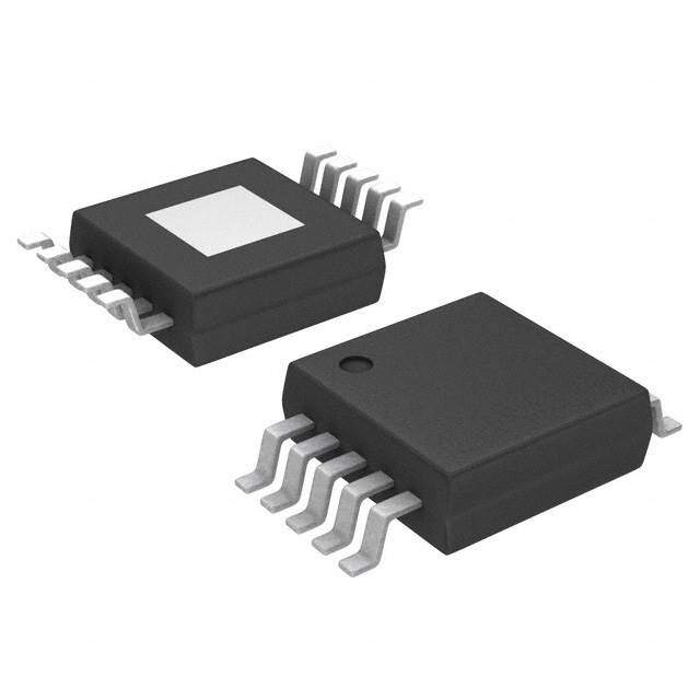
| 描述 | IC REG BUCK ADJ 1.5A 10MSOP稳压器—开关式稳压器 AC 3.5-42V Inp,1.5A |
| 产品分类 | |
| 品牌 | Texas Instruments |
| 产品手册 | http://www.ti.com/lit/gpn/tps54140-q1 |
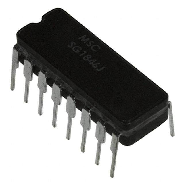
| 产品图片 |
|
| rohs | 符合RoHS无铅 / 符合限制有害物质指令(RoHS)规范要求 |
| 产品系列 | 电源管理 IC,稳压器—开关式稳压器,Texas Instruments TPS54140QDGQRQ1SWIFT™, Eco-Mode™ |
| 数据手册 | |
| 产品型号 | TPS54140QDGQRQ1 |
| PWM类型 | 电流模式 |
| 产品培训模块 | http://www.digikey.cn/PTM/IndividualPTM.page?site=cn&lang=zhs&ptm=16804 |
| 产品目录页面 | |
| 产品种类 | 稳压器—开关式稳压器 |
| 供应商器件封装 | 10-MSOP-PowerPad |
| 关闭 | Shutdown |
| 其它名称 | 296-25230-6 |
| 制造商产品页 | http://www.ti.com/general/docs/suppproductinfo.tsp?distId=10&orderablePartNumber=TPS54140QDGQRQ1 |
| 包装 | Digi-Reel® |
| 同步整流器 | 无 |
| 商标 | Texas Instruments |
| 商标名 | STEP-DOWN SWIFT, Eco-mode |
| 安装类型 | 表面贴装 |
| 安装风格 | SMD/SMT |
| 封装 | Reel |
| 封装/外壳 | 10-TFSOP,10-MSOP(0.118",3.00mm 宽)裸焊盘 |
| 封装/箱体 | HVSSOP-10 |
| 工作温度 | -40°C ~ 150°C |
| 工作温度范围 | - 40 C to + 150 C |
| 工厂包装数量 | 2500 |
| 开关频率 | 2.5 MHz |
| 拓扑结构 | Buck |
| 最大工作温度 | + 150 C |
| 最大输入电压 | 42 V |
| 最小工作温度 | - 40 C |
| 最小输入电压 | 3.5 V |
| 标准包装 | 1 |
| 电压-输入 | 3.5 V ~ 42 V |
| 电压-输出 | 0.8 V ~ 39 V |
| 电流-输出 | 1.5A |
| 电源电压-最小 | 3.5 V |
| 电源电流 | 116 uA |
| 类型 | 降压(降压) |
| 系列 | TPS54140-Q1 |
| 设计资源 | http://www.digikey.com/product-highlights/cn/zh/texas-instruments-webench-design-center/3176 |
| 输入电压 | 3.5 V to 42 V |
| 输出数 | 1 |
| 输出电压 | 0.8 V to 39 V |
| 输出电流 | 1.5 A |
| 输出端数量 | 1 Output |
| 输出类型 | 可调式 |
| 配用 | /product-detail/zh/TPS54140EVM-429/296-31178-ND/2232808 |
| 频率-开关 | 581kHz |


- 商务部:美国ITC正式对集成电路等产品启动337调查
- 曝三星4nm工艺存在良率问题 高通将骁龙8 Gen1或转产台积电
- 太阳诱电将投资9.5亿元在常州建新厂生产MLCC 预计2023年完工
- 英特尔发布欧洲新工厂建设计划 深化IDM 2.0 战略
- 台积电先进制程称霸业界 有大客户加持明年业绩稳了
- 达到5530亿美元!SIA预计今年全球半导体销售额将创下新高
- 英特尔拟将自动驾驶子公司Mobileye上市 估值或超500亿美元
- 三星加码芯片和SET,合并消费电子和移动部门,撤换高东真等 CEO
- 三星电子宣布重大人事变动 还合并消费电子和移动部门
- 海关总署:前11个月进口集成电路产品价值2.52万亿元 增长14.8%


PDF Datasheet 数据手册内容提取
TPS54140-Q1 www.ti.com SLVSA24C –OCTOBER2009–REVISEDAUGUST2012 1.5-A 42-V STEP-DOWN SWIFT™ DC/DC CONVERTER WITH Eco-mode™ CONTROL CheckforSamples:TPS54140-Q1 FEATURES • AdjustableUndervoltageLockoutVoltageand 1 Hysteresis • QualifiedforAutomotiveApplications 2 • 0.8-VInternalVoltageReference • 3.5-Vto42-VInputVoltageRange • SupportedbySwitcherPro™SoftwareTool • 200-mΩHigh-SideMOSFET (http://focus.ti.com/docs/toolsw/folders/print/s • HighEfficiencyatLightLoadsWithPulse- witcherpro.html) SkippingEco-mode™ControlScheme • ForSWIFT™Documentation,SeetheTI • 116-μAOperatingQuiescentCurrent Websiteathttp://www.ti.com/swift • 1.3-μAShutdownCurrent • 100-kHzto2.5-MHzSwitchingFrequency APPLICATIONS • SynchronizestoExternalClock • 12-Vand24-VIndustrialandCommercialLow • AdjustableSlowStart/Sequencing PowerSystems • UndervoltageandOvervoltagePower-good • AftermarketAutomotiveAccessories:Video, Output GPS,Entertainment DESCRIPTION The TPS54140-Q1 device is a 42-V 1.5-A step-down regulator with an integrated high-side MOSFET. Current- mode control provides simple external compensation and flexible component selection. A low-ripple pulse-skip mode reduces the no load, input supply current to 116 μA. Using the enable pin, shutdown supply current is reducedto1.3μA. Undervoltage lockout is internally set at 2.5 V, but can be increased using the enable pin. The output voltage startup ramp is controlled by the slow start pin that can also be configured for sequencing or tracking. An open- drainpowergoodsignalindicatestheoutputiswithin92%to109%ofitsnominalvoltage. A wide switching frequency range allows efficiency and external component size to be optimized. Frequency fold backandthermalshutdownprotectsthepartduringanoverloadcondition. The TPS54140-Q1 is available in a 10-pin thermally enhanced MSOP PowerPAD™ package (DGQ) and a 10- pinSONpackage(DRC). SIMPLIFIEDSCHEMATIC EFFICIENCY vs VIN PWRGD LOAD CURRENT 90 TPS54140 85 80 EN BOOT SS/TR PH Efficiency - % 677505 RT/CLK 60 VI= 12 V, COMP VO= 3.3 V, VSENSE 55 fsw= 1200 kHz 50 0 0.25 0.50 0.75 1 1.25 1.50 1.75 2 GND Load Current -A 1 Pleasebeawarethatanimportantnoticeconcerningavailability,standardwarranty,anduseincriticalapplicationsof TexasInstrumentssemiconductorproductsanddisclaimerstheretoappearsattheendofthisdatasheet. Eco-mode,SwitcherPro,SWIFT,PowerPADaretrademarksofTexasInstruments. 2 PRODUCTIONDATAinformationiscurrentasofpublicationdate. Copyright©2009–2012,TexasInstrumentsIncorporated Products conform to specifications per the terms of the Texas Instruments standard warranty. Production processing does not necessarilyincludetestingofallparameters.
TPS54140-Q1 SLVSA24C –OCTOBER2009–REVISEDAUGUST2012 www.ti.com This integrated circuit can be damaged by ESD. Texas Instruments recommends that all integrated circuits be handled with appropriateprecautions.Failuretoobserveproperhandlingandinstallationprocedurescancausedamage. ESDdamagecanrangefromsubtleperformancedegradationtocompletedevicefailure.Precisionintegratedcircuitsmaybemore susceptibletodamagebecauseverysmallparametricchangescouldcausethedevicenottomeetitspublishedspecifications. ORDERINGINFORMATION(1)(2) T PACKAGE ORDERABLEPARTNUMBER TOP-SIDEMARKING J MSOP–DGQ Reelof2500 TPS54140QDGQRQ1 5414Q –40°Cto150°C SON–DRC Reelof3000 TPS54140QDRCRQ1 5414Q (1) Forthemostcurrentpackageandorderinginformation,seethePackageOptionAddendumattheendofthisdocument,orseetheTI websiteatwww.ti.com. (2) Packagedrawings,thermaldata,andsymbolizationareavailableatwww.ti.com/packaging. ABSOLUTE MAXIMUM RATINGS(1) overoperatingtemperaturerange(unlessotherwisenoted) VIN –0.3Vto47V EN(2) –0.3Vto5V BOOT 55V VSENSE –0.3Vto3V V Inputvoltage IN COMP –0.3Vto3V PWRGD –0.3Vto6V SS/TR –0.3Vto3V RT/CLK –0.3Vto3.6V PHtoBOOT 8V –0.6Vto47V V Outputvoltage 200ns –1Vto47V OUT PH 30ns –2Vto47V Maximumdcvoltage,T =-40°C -0.85V J V Differentialvoltage PADtoGND ±200mV DIFF EN 100μA BOOT 100mA I Sourcecurrent VSENSE 10μA SOURCE PH CurrentLimit RT/CLK 100μA VIN CurrentLimit COMP 100μA I Sinkcurrent SINK PWRGD 10mA SS/TR 200μA Human-BodyModel(HBM)QSS009-105(JESD22-A114A) 500V ESD Electrostaticdischargeprotection MachineModel(MM)QSS009-105(JESD22-A115A) 50V Charged-DeviceModel(CDM)QSS009-147(JESD22-C101B.01) 1000V T Operatingjunctiontemperaturerange –40°Cto150°C J T Storagetemperaturerange –65°Cto150°C STG (1) StressesbeyondthoselistedunderAbsoluteMaximumRatingsmaycausepermanentdamagetothedevice.Thesearestressratings only,andfunctionaloperationofthedeviceattheseoranyotherconditionsbeyondthoseindicatedisnotimplied.Exposurebeyond absolutemaximumratedconditionsforextendedperiodsmayaffectdevicereliability. (2) SeeEnableandAdjustingUndervoltageLockoutfordetails. 2 Copyright©2009–2012,TexasInstrumentsIncorporated
TPS54140-Q1 www.ti.com SLVSA24C –OCTOBER2009–REVISEDAUGUST2012 THERMAL INFORMATION TPS54140-Q1 THERMALMETRIC(1)(2) DGQ DRC UNITS 10PINS 10PINS θ Junction-to-ambientthermalresistance(standardboard) 62.5 56.5 JA θ Junction-to-ambientthermalresistance(customboard)(3) 57 61.5 JA θ Junction-to-case(top)thermalresistance 83 52.1 JCtop θ Junction-to-boardthermalresistance 28 20.6 °C/W JB ψ Junction-to-topcharacterizationparameter 1.7 0.9 JT ψ Junction-to-boardcharacterizationparameter 20.1 20.8 JB θ Junction-to-case(bottom)thermalresistance 21 5.2 JCbot (1) Formoreinformationabouttraditionalandnewthermalmetrics,seetheICPackageThermalMetricsapplicationreport,SPRA953. (2) PowerratingataspecificambienttemperatureT shouldbedeterminedwithajunctiontemperatureof150°C.Thisisthepointwhere A distortionstartstosubstantiallyincrease.Seepowerdissipationestimateinapplicationsectionofthisdatasheetformoreinformation. (3) Testboardsconditions: (a)3inchesx3inches,2layers,thickness:0.062inch (b) 2oz.coppertraceslocatedonthetopofthePCB (c) 2oz.coppergroundplane,bottomlayer (d)6thermalvias(13mil)locatedunderthedevicepackage ELECTRICAL CHARACTERISTICS T =–40°Cto150°C,VIN=3.5Vto42V(unlessotherwisenoted) J PARAMETER TESTCONDITIONS MIN TYP MAX UNIT SUPPLYVOLTAGE(VINPIN) Operatinginputvoltage 3.5 42 V Internalundervoltagelockout Novoltagehysteresis,risingandfalling 2.5 V threshold EN=0V,25°C,3.5V≤VIN≤42V 1.3 4 Shutdownsupplycurrent EN=0V,125°C,3.5V≤VIN≤42V 1.9 6.5 μA Operating:nonswitchingsupply VSENSE=0.83V,VIN=12V,25°C 116 136 current ENABLEANDUVLO(ENPIN) Enablethresholdvoltage Novoltagehysteresis,risingandfalling,25°C 0.9 1.25 1.55 V Enablethreshold+50mV –3.8 Inputcurrent μA Enablethreshold–50mV –0.9 Hysteresiscurrent –2.9 μA VOLTAGEREFERENCE T =25°C 0.792 0.8 0.808 J Voltagereference V 0.784 0.8 0.816 HIGH-SIDEMOSFET VIN=3.5V,BOOT-PH=3V 300 On-resistance mΩ VIN=12V,BOOT-PH=6V 200 410 ERRORAMPLIFIER Inputcurrent 50 nA Erroramplifiertransconductance(g ) –2μA<I <2μA,V =1V 97 μMhos m COMP COMP Erroramplifiertransconductance(gm) –2μA<ICOMP<2μA,VCOMP=1V, 26 μMhos duringslowstart V =0.4V VSENSE Erroramplifierdcgain V =0.8V 10000 V/V VSENSE Erroramplifierbandwidth 2700 kHz Erroramplifiersource/sink V =1V,100mVoverdrive ±7 μA (COMP) COMPtoswitchcurrent 6 A/V transconductance Copyright©2009–2012,TexasInstrumentsIncorporated 3
TPS54140-Q1 SLVSA24C –OCTOBER2009–REVISEDAUGUST2012 www.ti.com ELECTRICAL CHARACTERISTICS (continued) T =–40°Cto150°C,VIN=3.5Vto42V(unlessotherwisenoted) J PARAMETER TESTCONDITIONS MIN TYP MAX UNIT CURRENTLIMIT Currentlimitthreshold VIN=12V,T =25°C 1.8 2.7 A J THERMALSHUTDOWN Thermalshutdown 182 °C TIMINGRESISTORANDEXTERNALCLOCK(RT/CLKPIN) SwitchingfrequencyrangeusingRT VIN=12V 100 2500 kHz mode f Switchingfrequency VIN=12V,R =200kΩ 450 581 720 kHz SW T Switchingfrequencyrangeusing VIN=12V 300 2200 kHz CLKmode MinimumCLKpulsewidth 40 ns RT/CLKhighthreshold VIN=12V 1.9 2.2 V RT/CLKlowthreshold VIN=12V 0.45 0.7 V RT/CLKfallingedgetoPHrising Measuredat500kHzwithRTresistorinseries 60 ns edgedelay PLLlockintime Measuredat500kHz 100 μs SLOWSTARTANDTRACKING(SS/TR) Chargecurrent V =0.4V 2 μA SS/TR SS/TR-to-VSENSEmatching V =0.4V 45 mV SS/TR SS/TR-to-referencecrossover 98%nominal 1 V SS/TRdischargecurrent(overload) VSENSE=0V,V(SS/TR)=0.4V 112 μA SS/TRdischargevoltage VSENSE=0V 54 mV POWER-GOOD(PWRGDPIN) VSENSEfalling(Fault) 92 VSENSErising(Good) 94 V VSENSEthreshold VSENSE VSENSErising(Fault) 109 % VSENSEfalling(Good) 107 Hysteresis VSENSEfalling 2 Outputhighleakage VSENSE=VREF,V(PWRGD)=5.5V,25°C 10 nA Onresistance I(PWRGD)=3mA,VSENSE<0.79V 50 Ω MinimumVINfordefinedoutput V(PWRGD)<0.5V,II(PWRGD)=100μA 0.95 1.5 V 4 Copyright©2009–2012,TexasInstrumentsIncorporated
TPS54140-Q1 www.ti.com SLVSA24C –OCTOBER2009–REVISEDAUGUST2012 DEVICE INFORMATION PINFUNCTIONS PIN I/O DESCRIPTION NAME NO. AbootstrapcapacitorisrequiredbetweenBOOTandPH.Ifthevoltageonthiscapacitorisbelowthe BOOT 1 O minimumrequiredbytheoutputdevice,theoutputisforcedtoswitchoffuntilthecapacitorisrefreshed. Erroramplifieroutput,andinputtotheoutputswitchcurrentcomparator.Connectfrequencycompensation COMP 8 O componentstothispin. Enablepin,internalpullupcurrentsource.Pullbelow1.2Vtodisable.Floattoenable.Adjusttheinput EN 3 I undervoltagelockoutwithtworesistors. GND 9 – Ground PH 10 I Thesourceoftheinternalhigh-sidepowerMOSFET. Anopendrainoutput,assertslowifoutputvoltageislowduetothermalshutdown,dropout,over-voltageor PWRGD 6 O ENshutdown. ResistorTimingandExternalClock.Aninternalamplifierholdsthispinatafixedvoltagewhenusingan externalresistortogroundtosettheswitchingfrequency.IfthepinispulledabovethePLLupperthreshold, RT/CLK 5 I amodechangeoccursandthepinbecomesasynchronizationinput.Theinternalamplifierisdisabledand thepinisahighimpedanceclockinputtotheinternalPLL.Ifclockingedgesstop,theinternalamplifierisre- enabledandthemodereturnstoaresistorsetfunction. Slow-startandTracking.Anexternalcapacitorconnectedtothispinsetstheoutputrisetime.Sincethe SS/TR 4 I voltageonthispinoverridestheinternalreference,itcanbeusedfortrackingandsequencing. VIN 2 I Inputsupplyvoltage,3.5Vto42V. VSENSE 7 I Invertingnodeofthetransconductance(gm)erroramplifier. ThermalPad – GNDpinmustbeelectricallyconnectedtotheexposedpadontheprintedcircuitboardforproperoperation. Copyright©2009–2012,TexasInstrumentsIncorporated 5
TPS54140-Q1 SLVSA24C –OCTOBER2009–REVISEDAUGUST2012 www.ti.com FUNCTIONALBLOCKDIAGRAM PWRGD EN VIN 6 3 2 Shutdown Thermal Shutdown UVLO Enable UO Logic Comparator Shutdown Shutdown Logic OV Enable Threshold Boot Charge Voltage Minimum Boot Reference Clamp UVLO Current Pulse Sense ERROR Skip AMPLIFIER PWM VSENSE 7 Comparator 1 BOOT SS/TR 4 Logic And PWM Latch Shutdown Slope Compensation COMP 8 10 PH 11 POWERPAD Frequency Shift Overload Maximum Recovery Clamp Oscillator TPS54140Block Diagram 9 GND with PLL 5 RT/CLK 6 Copyright©2009–2012,TexasInstrumentsIncorporated
TPS54140-Q1 www.ti.com SLVSA24C –OCTOBER2009–REVISEDAUGUST2012 TYPICAL CHARACTERISTICS ONRESISTANCEvsJUNCTIONTEMPERATURE VOLTAGEREFERENCEvsJUNCTIONTEMPERATURE W 0.816 m 500 nce - VI= 12 V VI= 12 V a c Drain-Source On-State Resist 213527055 BOOT-PH = 3 V BOOT-PH = 6 V V- Voltage Reference - Vref 000...788900208 ati St N - O 0.784 DS 0 -50 -25 0 25 50 75 100 125 150 R -50 -25 0 25 50 75 100 125 150 TJ- Junction Temperature - °C TJ- Junction Temperature - °C Figure1. Figure2. SWITCHCURRENTLIMITvsJUNCTIONTEMPERATURE SWITCHINGFREQUENCYvsJUNCTIONTEMPERATURE 3.5 610 V= 12 V, V= 12 V I I RT= 200 kW 600 Hz k A 3 cy - 590 nt - uen e q Switch Curr2.5 witching Fre 557800 S - fs 560 2 550 -50 -25 0 25 50 75 100 125 150 -50 -25 0 25 50 75 100 125 150 TJ- Junction Temperature - °C TJ- Junction Temperature - °C Figure3. Figure4. SWITCHINGFREQUENCYvsRT/CLKRESISTANCEHIGH SWITCHINGFREQUENCYvsRT/CLKRESISTANCELOW FREQUENCYRANGE FREQUENCYRANGE 2500 1000 VI= 12 V, VI= 12 V, TJ= 25°C TJ= 25°C Hz 2000 Hz 800 witching Frequency - k 11050000 witching Frequency - k 460000 S S f- s 500 f- s 200 0 0 0 25 50 75 100 125 150 175 200 100 200 300 400 500 600 700 800 900 1000 RT/CLK - Resistance - kW RT/CLK - Resistance - kW Figure5. Figure6. Copyright©2009–2012,TexasInstrumentsIncorporated 7
TPS54140-Q1 SLVSA24C –OCTOBER2009–REVISEDAUGUST2012 www.ti.com TYPICAL CHARACTERISTICS (continued) EATRANSCONDUCTANCEDURINGSLOWSTARTvs JUNCTIONTEMPERATURE EATRANSCONDUCTANCEvsJUNCTIONTEMPERATURE 40 150 V= 12 V I V= 12 V I 130 30 110 V V A/ A/ m m m - m - g g 90 20 70 10 50 -50 -25 0 25 50 75 100 125 150 -50 -25 0 25 50 75 100 125 150 TJ- Junction Temperature - °C TJ- Junction Temperature - °C Figure7. Figure8. ENPINVOLTAGEvsJUNCTIONTEMPERATURE ENPINCURRENTvsJUNCTIONTEMPERATURE 1.40 -3.25 V= 12 V VI= 12 V, I VI(EN)=Threshold +50 mV -3.5 V1.30 d - ol A h m EN - Thres1.20 I-(EN)-3.75 -4 1.10 -4.25 -50 -25 0 25 50 75 100 125 150 -50 -25 0 25 50 75 100 125 150 TJ- Junction Temperature - °C TJ- Junction Temperature - °C Figure9. Figure10. ENPINCURRENTvsJUNCTIONTEMPERATURE SS/TRCHARGECURRENTvsJUNCTIONTEMPERATURE -0.8 -1 VI= 12 V, VI= 12 V VI(EN)=Threshold -50 mV -0.85 -1.5 Am Am I-(EN)-0.9 I-(SS/TR) -2 -0.95 -2.5 -1 -3 -50 -25 0 25 50 75 100 125 150 -50 -25 0 25 50 75 100 125 150 TJ- Junction Temperature - °C TJ- Junction Temperature - °C Figure11. Figure12. 8 Copyright©2009–2012,TexasInstrumentsIncorporated
TPS54140-Q1 www.ti.com SLVSA24C –OCTOBER2009–REVISEDAUGUST2012 TYPICAL CHARACTERISTICS (continued) SS/TRDISCHARGECURRENTvsJUNCTION TEMPERATURE SWITCHINGFREQUENCYvsVSENSE 120 100 VI= 12 V VI= 12 V, T = 25°C J 80 115 w I-AmI(SS/TR)110 % of Nominal fs 4600 105 20 100 0 -50 -25 0 25 50 75 100 125 150 0 0.2 0.4 0.6 0.8 TJ- Junction Temperature - °C VSENSE- V Figure13. Figure14. SHUTDOWNSUPPLYCURRENTvsJUNCTION TEMPERATURE SHUTDOWNSUPPLYCURRENTvsINPUTVOLTAGE(V ) in 2 2 V= 12 V I T = 25°C J 1.5 1.5 A A m m I-(VIN) 1 I-(VIN) 1 0.5 0.5 0 0 -50 -25 0 25 50 75 100 125 150 0 10 20 30 40 TJ- Junction Temperature - °C VI- Input Voltage - V Figure15. Figure16. VINSUPPLYCURRENTvsJUNCTIONTEMPERATURE VINSUPPLYCURRENTvsINPUTVOLTAGE 140 140 VI= 12 V, TJ= 25oC, VI(VSENSE)= 0.83 V VI(VSENSE)= 0.83 V 130 130 120 120 A A m m I-(VIN) 110 I-(VIN) 110 100 100 90 90 -50 -25 0 25 50 75 100 125 150 0 20 40 TJ- Junction Temperature - °C VI- Input Voltage - V Figure17. Figure18. Copyright©2009–2012,TexasInstrumentsIncorporated 9
TPS54140-Q1 SLVSA24C –OCTOBER2009–REVISEDAUGUST2012 www.ti.com TYPICAL CHARACTERISTICS (continued) PWRGDONRESISTANCEvsJUNCTIONTEMPERATURE PWRGDTHRESHOLDvsJUNCTIONTEMPERATURE 100 115 VI= 12 V VI= 12 V 80 ef110 VSENSE Rising Vr of % 105 VSENSE Falling WN - 60 old - RDSO 40 GD Thresh 10905 VSENSE Rising R W P 20 90 VSENSE Falling 0 85 -50 -25 0 25 50 75 100 125 150 -50 -25 0 25 50 75 100 125 150 TJ- Junction Temperature - °C TJ- Junction Temperature - °C Figure19. Figure20. BOOT-PHUVLOvsJUNCTIONTEMPERATURE INPUTVOLTAGE(UVLO)vsJUNCTIONTEMPERATURE 3 2.3 2.75 V - 2.1 VI(BOOT-PH) V- VI(VIN) 2.50 1.9 2.25 1.7 2 -50 -25 0 25 50 75 100 125 150 -50 -25 0 25 50 75 100 125 150 TJ- Junction Temperature - °C TJ- Junction Temperature - °C Figure21. Figure22. SS/TRTOVSENSEOFFSETvsVSENSE SS/TRTOVSENSEOFFSETvsTEMPERATURE 600 60 V = 0.2 V V =12V (SS/TR) mV) 500 TIJN=25°C 55 VI= 12 V ( d hol 400 50 res mV ageTh 300 Offset - 45 olt 40 V 200 et s 35 Off 100 30 -50 -25 0 25 50 75 100 125 150 0 0 200 400 600 800 TJ- Junction Temperature - °C VoltageSense(mV) Figure23. Figure24. 10 Copyright©2009–2012,TexasInstrumentsIncorporated
TPS54140-Q1 www.ti.com SLVSA24C –OCTOBER2009–REVISEDAUGUST2012 OVERVIEW The TPS54140-Q1 device is a 42-V, 1.5-A, step-down (buck) regulator with an integrated high side n-channel MOSFET. To improve performance during line and load transients the device implements a constant frequency, current mode control which reduces output capacitance and simplifies external frequency compensation design. The wide switching frequency of 100 kHz to 2500 kHz allows for efficiency and size optimization when selecting the output filter components. The switching frequency is adjusted using a resistor to ground on the RT/CLK pin. The device has an internal phase lock loop (PLL) on the RT/CLK pin that is used to synchronize the power switchturnontoafallingedgeofanexternalsystemclock. The TPS54140-Q1 has a default start up voltage of approximately 2.5 V. The EN pin has an internal pull-up current source that can be used to adjust the input voltage undervoltage lockout (UVLO) threshold with two external resistors. In addition, the pull up current provides a default condition. When the EN pin is floating the device will operate. The operating current is 116 μA when not switching and under no load. When the device is disabled,thesupplycurrentis1.3μA. The integrated 200 mΩ high side MOSFET allows for high efficiency power supply designs capable of delivering 1.5 amperes of continuous current to a load. The TPS54140-Q1 reduces the external component count by integrating the boot recharge diode. The bias voltage for the integrated high side MOSFET is supplied by a capacitor on the BOOT to PH pin. The boot capacitor voltage is monitored by an UVLO circuit and will turn the high side MOSFET off when the boot voltage falls below a preset threshold. The TPS54140-Q1 can operate at high duty cycles because of the boot UVLO. The output voltage can be stepped down to as low as the 0.8 V reference. The TPS54140-Q1 has a power-good comparator (PWRGD) which asserts when the regulated output voltage is less than 92% or greater than 109% of the nominal output voltage. The PWRGD pin is an open drain output which de-asserts when the VSENSE pin voltage is between 94% and 107% of the nominal output voltage allowingthepintotransitionhighwhenapull-upresistorisused. The TPS54140-Q1 minimizes excessive output overvoltage (OV) transients by taking advantage of the OV power-good comparator. When the OV comparator is activated, the high side MOSFET is turned off and masked fromturningonuntiltheoutputvoltageislowerthan107%. The SS/TR (slow start/tracking) pin is used to minimize inrush currents or provide power supply sequencing during power up. A small value capacitor should be coupled to the pin to adjust the slow start time. A resistor dividercanbecoupledtothepinforcriticalpowersupplysequencingrequirements.TheSS/TRpinisdischarged before the output powers up. This discharging ensures a repeatable restart after an over-temperature fault, UVLOfaultoradisabledcondition. The TPS54140-Q1, also, discharges the slow start capacitor during overload conditions with an overload recovery circuit. The overload recovery circuit will slow start the output from the fault voltage to the nominal regulation voltage once a fault condition is removed. A frequency foldback circuit reduces the switching frequencyduringstartupandovercurrentfaultconditionstohelpcontroltheinductorcurrent. Copyright©2009–2012,TexasInstrumentsIncorporated 11
TPS54140-Q1 SLVSA24C –OCTOBER2009–REVISEDAUGUST2012 www.ti.com DETAILED DESCRIPTION Fixed Frequency PWM Control The TPS54140-Q1 uses an adjustable fixed frequency, peak current mode control. The output voltage is compared through external resistors on the VSENSE pin to an internal voltage reference by an error amplifier which drives the COMP pin. An internal oscillator initiates the turn on of the high side power switch. The error amplifier output is compared to the high side power switch current. When the power switch current reaches the COMP voltage level the power switch is turned off. The COMP pin voltage will increase and decrease as the output current increases and decreases. The device implements a current limit by clamping the COMP pin voltagetoamaximumlevel.TheEco-Mode™isimplementedwithaminimumclampontheCOMPpin. Slope Compensation Output Current The TPS54140-Q1 adds a compensating ramp to the switch current signal. This slope compensation prevents sub-harmonicoscillations.Theavailablepeakinductorcurrentremainsconstantoverthefulldutycyclerange. Pulse Skip Eco-Mode The TPS54140-Q1 enters the pulse skip mode when the voltage on the COMP pin is the minimum clamp value. The TPS54140-Q1 operates in a pulse skip mode at light load currents to improve efficiency. The peak switch current during the pulse skip mode will be the greater value of 50 mA or the peak inductor current that is a function of the minimum on time, input voltage, output voltage and inductance value. When the load current is low and the output voltage is within regulation the device will enter a sleep mode and draw only 116 μA input quiescentcurrent.Whilethedeviceisinsleepmodetheoutputpowerisdeliveredbytheoutputcapacitor.Asthe load current decreases, the time the output capacitor supplies the load current increases and the switching frequency decreases reducing gate drive and switching losses. As the output voltage drops, the TPS54140-Q1 wakes up from the sleep mode and the power switch turns on to recharge the output capacitor, see Figure 25. The internal PLL remains operating when in sleep mode. When operating at light load currents in the pulse skip modetheswitchingtransitionsoccursynchronouslywiththeexternalclocksignal. VOUT(ac) IL PH Figure25. PulseSkipModeOperation 12 Copyright©2009–2012,TexasInstrumentsIncorporated
TPS54140-Q1 www.ti.com SLVSA24C –OCTOBER2009–REVISEDAUGUST2012 DETAILED DESCRIPTION (continued) Bootstrap Voltage (BOOT) The TPS54140-Q1 has an integrated boot regulator and requires a small ceramic capacitor between the BOOT and PH pin to provide the gate drive voltage for the high side MOSFET. The value of the ceramic capacitor should be 0.1 μF. A ceramic capacitor with an X7R or X5R grade dielectric is recommended because of the stable characteristics over temperature and voltage. To improve drop out, the TPS54140-Q1 is designed to operate at 100% duty cycle as long as the BOOT to PH pin voltage is greater than 2.1 V. When the voltage from BOOT to PH drops below 2.1 V, the high side MOSFET is turned off using an UVLO circuit allowing for the low side diode to conduct which allows refreshing of the BOOT capacitor. Since the supply current sourced from the BOOT capacitor is low, the high side MOSFET can remain on for more switching cycles than it refreshes, thus, theeffectivedutycyclelimitationthatisattributedtothebootregulatorsystemishigh. Low Dropout Operation The duty cycle during dropout of the regulator will be mainly determined by the voltage drops across the power MOSFET, inductor, low side diode and printed circuit board resistance. During operating conditions in which the input voltage drops, the high side MOSFET can remain on for 100% of the duty cycle to maintain output regulationoruntiltheBOOTtoPHvoltagefallsbelow2.1V. Once the high side is off, the low side diode will conduct and the BOOT capacitor will be recharged. During this boot capacitor recharge time, the inductor current will ramp down until the high side MOSFET turns on. The recharge time is longer than the typical high side off time of previous switching cycles, and thus, the inductor current ripple is larger resulting in more ripple voltage on the output. The recharge time is a function of the input voltage,bootcapacitorvalue,andtheimpedanceoftheinternalbootrechargediode. Attention needs to be taken in maximum duty cycle applications which experience extended time periods without a load current. When the voltage across the BOOT capacitors falls below the 2.1 V threshold in applications that have a difference in the input voltage and output voltage that is less than 3 V, the high side MOSFET will be turned off but there is not enough current in the inductor to pull the PH pin down to recharge the boot capacitor. The regulator will not switch because the boot capacitor is less than 2.1 V and the output capacitor will decay until the difference in the input voltage and output voltage is 2.1 V. At this time the boot undervoltage lockout is exceededandthedevicewillswitchuntilthedesiredoutputvoltageisreached. The start and stop voltages are shown in Figure 26 and Figure 27 for 3.3-V and 5-V applications. The voltages are plotted versus the load current. The start voltage is defined as the input voltage needed to regulate within 1%.Thestopvoltageisdefinedastheinputvoltageatwhichtheoutputdropsby5%orstopsswitching. 4 5.6 VO= 3.3 V VO= 5 V 3.8 5.4 V V Voltage - 3.6 Start Voltage - 5.2 Start V- Input I 3.4 Stop V- Input I 5 Stop 3.2 4.8 3 4.6 0 0.05 0.10 0.15 0.20 0 0.05 0.10 0.15 0.20 IO- Output Current -A IO- Output Current -A Figure26.3.3-VStart/StopVoltage Figure27.5-VStart/StopVoltage Copyright©2009–2012,TexasInstrumentsIncorporated 13
TPS54140-Q1 SLVSA24C –OCTOBER2009–REVISEDAUGUST2012 www.ti.com DETAILED DESCRIPTION (continued) Error Amplifier The TPS54140-Q1 has a transconductance amplifier for the error amplifier. The error amplifier compares the VSENSE voltage to the lower of the SS/TR pin voltage or the internal 0.8-V voltage reference. The transconductance (gm) of the error amplifier is 97 μA/V during normal operation. During the slow start operation, thetransconductanceisafractionofthenormaloperatinggm.WhenthevoltageoftheVSENSEpinisbelow0.8 VandthedeviceisregulatingusingtheSS/TRvoltage,thegmis25μA/V. The frequency compensation components (capacitor, series resistor and capacitor) are added from the COMP pintoground. Voltage Reference The voltage reference system produces a precise ±2% voltage reference over temperature by scaling the output ofatemperaturestablebandgapcircuit. Adjusting the Output Voltage The output voltage is set with a resistor divider from the output node to the VSENSE pin. It is recommended to use 1% tolerance or better divider resistors. Start with a 10 kΩ for the R2 resistor and use the Equation 1 to calculate R1. To improve efficiency at very light loads consider using larger value resistors. If the values are too high the regulator will be more susceptible to noise and voltage errors from the VSENSE input current will be noticeable æVout - 0.8Vö R1=R2 ´ ç ÷ è 0.8V ø (1) Enable and Adjusting Undervoltage Lockout The TPS54140-Q1 is disabled when the VIN pin voltage falls below 2.5 V. If an application requires a higher undervoltage lockout (UVLO), use the EN pin as shown in Figure 28 to adjust the input voltage UVLO by using the two external resistors. Though it is not necessary to use the UVLO adjust resistors, for operation it is highly recommended to provide consistent power up behavior. The EN pin has an internal pull-up current source, I1, of 0.9 μA that provides the default condition of the TPS54140-Q1 operating when the EN pin floats. Once the EN pin voltage exceeds 1.25 V, an additional 2.9 μA of hysteresis, I , is added. This additional current facilitates HYS input voltage hysteresis. Use Equation 2 to set the external hysteresis for the input voltage. Use Equation 3 to settheinputstartvoltage. TPS54140 VIN Ihys I1 R1 0.9mA 2.9mA + R2 EN 1.25 V - Figure28. AdjustableUndervoltageLockout(UVLO) V -V R1= START STOP I HYS (2) V R2= ENA V -V START ENA +I R1 1 (3) 14 Copyright©2009–2012,TexasInstrumentsIncorporated
TPS54140-Q1 www.ti.com SLVSA24C –OCTOBER2009–REVISEDAUGUST2012 DETAILED DESCRIPTION (continued) Another technique to add input voltage hysteresis is shown in Figure 29. This method may be used, if the resistance values are high from the previous method and a wider voltage hysteresis is needed. The resistor R3 sourcesadditionalhysteresiscurrentintotheENpin. TPS54140 VIN Ihys R1 I1 2.9mA 0.9mA + R2 EN 1.25 V - VOUT R3 Figure29.AddingAdditionalHysteresis V -V R1= START STOP V I + OUT HYS R3 (4) V R2= ENA V -V V START ENA +I - ENA R1 1 R3 (5) Do not place a low-impedance voltage source with greater than 5 V directly on the EN pin. Do not place a capacitor directly on the EN pin if V > 5 V when using a voltage divider to adjust the start and stop voltage. EN The node voltage, (see Figure 30) must remain equal to or less than 5.8 V. The zener diode can sink up to 100 μA. The EN pin voltage can be greater than 5 V if the V voltage source has a high impedance and does not IN sourcemorethan100μAintotheENpin. V IN I A R UVLO1 EN 10kW Node 3 I IB R C 5.8V UVLO2 UDG-10065 Figure30. NodeVoltage Copyright©2009–2012,TexasInstrumentsIncorporated 15
TPS54140-Q1 SLVSA24C –OCTOBER2009–REVISEDAUGUST2012 www.ti.com DETAILED DESCRIPTION (continued) Slow Start/Tracking Pin (SS/TR) The TPS54140-Q1 effectively uses the lower voltage of the internal voltage reference or the SS/TR pin voltage as the reference voltage of the power-supply and regulates the output accordingly. A capacitor on the SS/TR pin to ground implements a slow start time. The TPS54140-Q1 has an internal pull-up current source of 2 μA that charges the external slow start capacitor. The calculations for the slow start time (10% to 90%) are shown in Equation6.Thevoltagereference(V )is0.8Vandtheslowstartcurrent(I )is2μA.Theslowstartcapacitor REF SS shouldremainlowerthan0.47μFandgreaterthan0.47nF. Tss(ms) ´ Iss(mA) Css(nF)= Vref(V) ´ 0.8 (6) At power up, the TPS54140-Q1 will not start switching until the slow start pin is discharged to less than 40 mV to ensureaproperpowerup,seeFigure31. Also, during normal operation, the TPS54140-Q1 will stop switching and the SS/TR must be discharged to 40 mV,whentheVINUVLOisexceeded,ENpinpulledbelow1.25V,orathermalshutdowneventoccurs. The VSENSE voltage will follow the SS/TR pin voltage with a 45-mV offset up to 85% of the internal voltage reference. When the SS/TR voltage is greater than 85% on the internal reference voltage the offset increases as the effective system reference transitions from the SS/TR voltage to the internal voltage reference (see Figure23).TheSS/TRvoltagewillramplinearlyuntilclampedat1.7V. EN SS/TR V SENSE VOUT Figure31. OperationofSS/TRPinWhenStarting Overload Recovery Circuit The TPS54140-Q1 has an overload recovery (OLR) circuit. The OLR circuit will slow start the output from the overload voltage to the nominal regulation voltage once the fault condition is removed. The OLR circuit will discharge the SS/TR pin to a voltage slightly greater than the VSENSE pin voltage using an internal pull down of 100 μA when the error amplifier is changed to a high voltage from a fault condition. When the fault condition is removed,theoutputwillslowstartfromthefaultvoltagetonominaloutputvoltage. 16 Copyright©2009–2012,TexasInstrumentsIncorporated
TPS54140-Q1 www.ti.com SLVSA24C –OCTOBER2009–REVISEDAUGUST2012 DETAILED DESCRIPTION (continued) Sequencing Many of the common power supply sequencing methods can be implemented using the SS/TR, EN and PWRGD pins. The sequential method can be implemented using an open drain output of a power-on reset pin of another device. The sequential method is illustrated in Figure 32 using two TPS54140-Q1 devices. The power good is coupled to the EN pin on the TPS54140-Q1 which will enable the second power supply once the primary supply reaches regulation. If needed, a 1-nF ceramic capacitor on the EN pin of the second power supply will provide a 1-msstartupdelay.Figure33showstheresultsofFigure32. TPS54140 PWRGD EN EN EN1 SS/TR SS/TR PWRGD1 PWRGD VOUT1 VOUT2 Figure32.SchematicforSequentialStart-Up Figure33.SequentialStartupusingENand Sequence PWRGD TTPPSS5544114600 3 EN EN1, EN2 4 SS/TR 6 PWRGD VOUT1 TTPPSS5544116400 VOUT2 3 EN 4 SS/TR 6 PWRGD Figure34.SchematicforRatiometricStart-Up Figure35.RatiometricStartupUsingCoupled UsingCoupledSS/TRPins SS/TRPins Copyright©2009–2012,TexasInstrumentsIncorporated 17
TPS54140-Q1 SLVSA24C –OCTOBER2009–REVISEDAUGUST2012 www.ti.com DETAILED DESCRIPTION (continued) Figure 34 shows a method for ratiometric start up sequence by connecting the SS/TR pins together. The regulator outputs will ramp up and reach regulation at the same time. When calculating the slow start time the pullupcurrentsourcemustbedoubledinEquation6.Figure35showstheresultsofFigure34. TPS54140 EN VOUT1 SS/TR PWRGD TPS54140 EN VOUT2 R1 SS/TR R2 PWRGD R3 R4 Figure36. SchematicforRatiometricandSimultaneousStart-UpSequence Ratiometric and simultaneous power supply sequencing can be implemented by connecting the resistor network of R1 and R2 shown in Figure 36 to the output of the power supply that needs to be tracked or another voltage reference source. Using Equation 7 and Equation 8, the tracking resistors can be calculated to initiate the V OUT2 slightly before, after or at the same time as V . Equation 9 is the voltage difference between V and V OUT1 OUT1 OUT2 atthe95%ofnominaloutputregulation. The ΔV variable is zero volts for simultaneous sequencing. To minimize the effect of the inherent SS/TR to VSENSE offset (V ) in the slow start circuit and the offset created by the pullup current source (I ) and SSOFFSET SS trackingresistors,theV andLSSareincludedasvariablesintheequations. SSOFFSET To design a ratio-metric start up in which the V voltage is slightly greater than the V voltage when V OUT2 OUT1 OUT2 reaches regulation, use a negative number in Equation 7 through Equation 9 for ΔV. Equation 9 will result in a positivenumberforapplicationswhichtheV isslightlylowerthanV whenV regulationisachieved. OUT2 OUT1 OUT2 Since the SS/TR pin must be pulled below 40 mV before starting after an EN, UVLO or thermal shutdown fault, careful selection of the tracking resistors is needed to ensure the device will restart after a fault. Make sure the calculated R1 value from Equation 7 is greater than the value calculated in Equation 10 to ensure the device can recoverfromafault. As the SS/TR voltage becomes more than 85% of the nominal reference voltage the V becomes larger SSOFFSET as the slow start circuits gradually handoff the regulation reference to the internal voltage reference. The SS/TR pin voltage needs to be greater than 1.3 V for a complete handoff to the internal voltage reference as shown in Figure23. Vout2+deltaV Vssoffset R1= ´ VREF Iss (7) VREF ´ R1 R2= Vout2+deltaV - VREF (8) 18 Copyright©2009–2012,TexasInstrumentsIncorporated
TPS54140-Q1 www.ti.com SLVSA24C –OCTOBER2009–REVISEDAUGUST2012 DETAILED DESCRIPTION (continued) deltaV=Vout1 - Vout2 (9) R1>2800 ´ Vout1 - 180 ´ deltaV (10) EN EN VOUT1 VOUT1 VOUT2 VOUT2 Figure37.RatiometricStartupwithV Leading Figure38.RatiometricStartupwithV Leading OUT2 OUT1 V V OUT1 OUT2 EN VOUT1 VOUT2 Figure39.SimultaneousStartupWithTrackingResistor Copyright©2009–2012,TexasInstrumentsIncorporated 19
TPS54140-Q1 SLVSA24C –OCTOBER2009–REVISEDAUGUST2012 www.ti.com DETAILED DESCRIPTION (continued) Constant Switching Frequency and Timing Resistor (RT/CLK Pin) The switching frequency of the TPS54140-Q1 is adjustable over a wide range from approximately 100 kHz to 2500 kHz by placing a resistor on the RT/CLK pin. The RT/CLK pin voltage is typically 0.5 V and must have a resistor to ground to set the switching frequency. To determine the timing resistance for a given switching frequency, use Equation 11 or the curves in Figure 40 or Figure 41. To reduce the solution size one would typically set the switching frequency as high as possible, but tradeoffs of the supply efficiency, maximum input voltageandminimumcontrollableontimeshouldbeconsidered. Theminimumcontrollableontimeistypically130nsandlimitsthemaximumoperatinginputvoltage. The maximum switching frequency is also limited by the frequency shift circuit. More discussion on the details of themaximumswitchingfrequencyislocatedbelow. 206033 RT (kOhm)= ¦sw (kHz)1.0888 (11) SWITCHINGFREQUENCY SWITCHINGFREQUENCY vs vs RT/CLKRESISTANCEHIGHFREQUENCYRANGE RT/CLKRESISTANCELOWFREQUENCYRANGE 2500 500 V= 12 V, I T = 25°C J V= 12 V, Hz 2000 Hz 400 TJI= 25°C witching Frequency - k 11050000 witching Frequency - k 230000 f- Ss 500 f- Ss 100 0 0 0 25 50 75 100 125 150 175 200 200 300 400 500 600 700 800 900 1000 1100 1200 RT/CLK - Clock Resistance - kW RT/CLK - Resistance - kW Figure40.HighRangeRT Figure41.LowRangeRT Overcurrent Protection and Frequency Shift The TPS54140-Q1 implements current mode control which uses the COMP pin voltage to turn off the high side MOSFET on a cycle by cycle basis. During each cycle the switch current and COMP pin voltage are compared, when the peak switch current intersects the COMP voltage, the high side switch is turned off. During overcurrent conditions that pull the output voltage low, the error amplifier will respond by driving the COMP pin high, increasing the switch current. The error amplifier output is clamped internally, which functions as a switch current limit. To increase the maximum operating switching frequency at high input voltages the TPS54140-Q1 implements a frequency shift. The switching frequency is divided by 8, 4, 2, and 1 as the voltage ramps from 0 to 0.8 volts on VSENSEpin. The device implements a digital frequency shift to enable synchronizing to an external clock during normal startup and fault conditions. Since the device can only divide the switching frequency by 8, there is a maximum inputvoltagelimitinwhichthedeviceoperatesandstillhavefrequencyshiftprotection. Duringshort-circuitevents(particularlywithhighinputvoltageapplications),thecontrolloophasafiniteminimum controllable on time and the output has a very low voltage. During the switch on time, the inductor current ramps to the peak current limit because of the high input voltage and minimum on time. During the switch off time, the inductor would normally not have enough off time and output voltage for the inductor to ramp down by the ramp upamount.Thefrequencyshifteffectivelyincreasestheofftimeallowingthecurrenttorampdown. 20 Copyright©2009–2012,TexasInstrumentsIncorporated
TPS54140-Q1 www.ti.com SLVSA24C –OCTOBER2009–REVISEDAUGUST2012 DETAILED DESCRIPTION (continued) Selecting the Switching Frequency The switching frequency that is selected should be the lower value of the two equations, Equation 12 and Equation13.Equation12isthemaximumswitchingfrequencylimitationsetbytheminimumcontrollableontime. Settingtheswitchingfrequencyabovethisvaluewillcausetheregulatortoskipswitchingpulses. Equation 13 is the maximum switching frequency limit set by the frequency shift protection. To have adequate output short circuit protection at high input voltages, the switching frequency should be set to be less than the ƒ frequency. In Equation 13, to calculate the maximum switching frequency one must take into account SW(maxshift) that the output voltage decreases from the nominal voltage to 0 volts, the ƒ integer increases from 1 to 8 DIV correspondingtothefrequencyshift. In Figure 42, the solid line illustrates a typical safe operating area regarding frequency shift and assumes the outputvoltageiszerovolts,andtheresistanceoftheinductoris0.1Ω,FETonresistanceof0.2Ωandthediode voltage drop is 0.5 V. The dashed line is the maximum switching frequency to avoid pulse skipping. Enter these equations in a spreadsheet or other software or use the SwitcherPro design software to determine the switching frequency. æ ö 1 I ´R +V +V f = ´ç L dc OUT d ÷ SW(maxskip) t çV -I ´R +V ÷ ON è IN L DS(on) d ø (12) fSWshift = fDIV ´æçIL´Rdc +VOUT(sc)+Vd ö÷ tON ç VIN-IL´RDS(on)+Vd ÷ è ø (13) I inductorcurrent L R inductorresistance dc V maximuminputvoltage IN V outputvoltage OUT V outputvoltageduringshort OUTSC V diodevoltagedrop d R switchonresistance DS(ON) t controllableontime ON ƒ frequencydivideequals(1,2,4,or8) DIV 2500 V = 3.3 V O Hz 2000 y - k Shift c n ue 1500 q Fre Skip g n hi 1000 c wit S - fs 500 0 10 20 30 40 VI- Input Voltage - V Figure42. MaximumSwitchingFrequencyvs.InputVoltage Copyright©2009–2012,TexasInstrumentsIncorporated 21
TPS54140-Q1 SLVSA24C –OCTOBER2009–REVISEDAUGUST2012 www.ti.com DETAILED DESCRIPTION (continued) How to Interface to RT/CLK Pin The RT/CLK pin can be used to synchronize the regulator to an external system clock. To implement the synchronization feature connect a square wave to the RT/CLK pin through the circuit network shown in Figure 43. The square wave amplitude must transition lower than 0.5 V and higher than 2.2 V on the RT/CLK pin and have an on time greater than 40 ns and an off time greater than 40 ns. The synchronization frequency range is 300 kHz to 2200 kHz. The rising edge of the PH will be synchronized to the falling edge of RT/CLK pin signal. The external synchronization circuit should be designed in such a way that the device will have the default frequency set resistor connected from the RT/CLK pin to ground should the synchronization signal turn off. It is recommended to use a frequency set resistor connected as shown in Figure 43 through a 50-Ω resistor to ground. The resistor should set the switching frequency close to the external CLK frequency. It is recommended to ac couple the synchronization signal through a 10-pF ceramic capacitor to RT/CLK pin and a 4-kΩ series resistor. The series resistor reduces PH jitter in heavy load applications when synchronizing to an external clock and in applications which transition from synchronizing to RT mode. The first time the CLK is pulled above the CLK threshold the device switches from the RT resistor frequency to PLL mode. The internal 0.5-V voltage source is removed and the CLK pin becomes high impedance as the PLL starts to lock onto the external signal. Since there is a PLL on the regulator the switching frequency can be higher or lower than the frequency set with the external resistor. The device transitions from the resistor mode to the PLL mode and then will increase or decreasetheswitchingfrequencyuntilthePLLlocksontotheCLKfrequencywithin100microseconds. When the device transitions from the PLL to resistor mode the switching frequency will slow down from the CLK frequency to 150 kHz, then reapply the 0.5-V voltage and the resistor will then set the switching frequency. The switching frequency is divided by 8, 4, 2, and 1 as the voltage ramps from 0- to 0.8-volts on VSENSE pin. The device implements a digital frequency shift to enable synchronizing to an external clock during normal startup and fault conditions. Figure 44, Figure 45 and Figure 46 show the device synchronized to an external system clockincontinuousconductionmode(CCM)discontinuousconduction(DCM)andpulseskipmode(PSM). TPS54140 10 pF 4 kW PLL R fset EXT RT/CLK Clock 50W Source Figure43. SynchronizingtoaSystemClock 22 Copyright©2009–2012,TexasInstrumentsIncorporated
TPS54140-Q1 www.ti.com SLVSA24C –OCTOBER2009–REVISEDAUGUST2012 DETAILED DESCRIPTION (continued) EXT EXT VOUT IL PH PH IL Figure44.PlotofSynchronizinginCCM Figure45.PlotofSynchronizinginDCM EXT IL PH Figure46.PlotofSynchronizinginPSM Power-good (PWRGD Pin) The PWRGD pin is an open drain output. Once the VSENSE pin is between 94% and 107% of the internal voltage reference the PWRGD pin is de-asserted and the pin floats. It is recommended to use a pull-up resistor between the values of 1 kΩ and 100 kΩ to a voltage source that is 5.5 V or less. The PWRGD is in a defined state once the V input voltage is greater than 1.5 V but with reduced current sinking capability. The PWRGD IN willachievefullcurrentsinkingcapabilityasV inputvoltageapproaches3V. IN Copyright©2009–2012,TexasInstrumentsIncorporated 23
TPS54140-Q1 SLVSA24C –OCTOBER2009–REVISEDAUGUST2012 www.ti.com DETAILED DESCRIPTION (continued) ThePWRGDpinispulledlowwhentheVSENSEislowerthan92%orgreaterthan109%ofthenominalinternal reference voltage. Also, the PWRGD is pulled low, if the UVLO or thermal shutdown are asserted or the EN pin pulledlow. Overvoltage Transient Protection The TPS54140-Q1 incorporates an overvoltage transient protection (OVTP) circuit to minimize voltage overshoot when recovering from output fault conditions or strong unload transients on power supply designs with low value output capacitance. For example, when the power supply output is overloaded the error amplifier compares the actual output voltage to the internal reference voltage. If the VSENSE pin voltage is lower than the internal reference voltage for a considerable time, the output of the error amplifier will respond by clamping the error amplifier output to a high voltage, thus requesting the maximum output current. Once the condition is removed, the regulator output rises and the error amplifier output transitions to the steady state duty cycle. In some applications, the power supply output voltage can respond faster than the error amplifier output can respond, this actuality leads to the possibility of an output overshoot. The OVTP feature minimizes the output overshoot, when using a low value output capacitor, by implementing a circuit to compare the VSENSE pin voltage to OVTP threshold which is 109% of the internal voltage reference. If the VSENSE pin voltage is greater than the OVTP threshold, the high side MOSFET is disabled preventing current from flowing to the output and minimizing output overshoot. When the VSENSE voltage drops lower than the OVTP threshold, the high side MOSFET is allowed toturnonatthenextclockcycle. Thermal Shutdown The device implements an internal thermal shutdown to protect itself if the junction temperature exceeds 182°C. The thermal shutdown forces the device to stop switching when the junction temperature exceeds the thermal trip threshold. Once the die temperature decreases below 182°C, the device reinitiates the power up sequence bydischargingtheSS/TRpin. Small Signal Model for Loop Response Figure 47 shows an equivalent model for the TPS54140-Q1 control loop which can be modeled in a circuit simulation program to check frequency response and dynamic load response. The error amplifier is a transconductance amplifier with a gm of 97 μA/V. The error amplifier can be modeled using an ideal voltage EA controlled current source. The resistor R and capacitor C model the open loop gain and frequency response of o o the amplifier. The 1-mV ac voltage source between the nodes a and b effectively breaks the control loop for the frequencyresponsemeasurements.Plottingc/ashowsthesmallsignalresponseofthefrequencycompensation. Plotting a/b shows the small signal response of the overall loop. The dynamic loop response can be checked by replacing R with a current source with the appropriate load step amplitude and step rate in a time domain L analysis.Thisequivalentmodelisonlyvalidforcontinuousconductionmodedesigns. 24 Copyright©2009–2012,TexasInstrumentsIncorporated
TPS54140-Q1 www.ti.com SLVSA24C –OCTOBER2009–REVISEDAUGUST2012 DETAILED DESCRIPTION (continued) PH V Power Stage O gm 6A/V ps a b R1 RESR COMP RL c VSENSE C 0.8 V OUT CO RO R3 gm ea C2 97mA/V R2 C1 Figure47. SmallSignalModelforLoopResponse Simple Small Signal Model for Peak Current Mode Control Figure 48 describes a simple small signal model that can be used to understand how to design the frequency compensation. The TPS54140-Q1 power stage can be approximated to a voltage-controlled current source (duty cycle modulator) supplying current to the output capacitor and load resistor. The control to output transfer function is shown in Equation 14 and consists of a dc gain, one dominant pole, and one ESR zero. The quotient of the change in switch current and the change in COMP pin voltage (node c in Figure 47) is the power stage transconductance. The gm for the TPS54140-Q1 is 6 A/V. The low-frequency gain of the power stage PS frequencyresponseistheproductofthetransconductanceandtheloadresistanceasshowninEquation15. Astheloadcurrentincreasesanddecreases,thelow-frequencygaindecreasesandincreases,respectively.This variation with the load may seem problematic at first glance, but fortunately the dominant pole moves with the load current (see Equation 16). The combined effect is highlighted by the dashed line in the right half of Figure 48. As the load current decreases, the gain increases and the pole frequency lowers, keeping the 0-dB crossover frequency the same for the varying load conditions which makes it easier to design the frequency compensation. The type of output capacitor chosen determines whether the ESR zero has a profound effect on the frequency compensation design. Using high ESR aluminum electrolytic capacitors may reduce the number frequency compensation components needed to stabilize the overall loop because the phase margin increases fromtheESRzeroatthelowerfrequencies(seeEquation17). Copyright©2009–2012,TexasInstrumentsIncorporated 25
TPS54140-Q1 SLVSA24C –OCTOBER2009–REVISEDAUGUST2012 www.ti.com DETAILED DESCRIPTION (continued) V O VC Adc R ESR fp R L gm ps C OUT fz Figure48.SimpleSmallSignalModelandFrequencyResponseforPeakCurrentModeControl æ s ö ç1+ ÷ VOUT = Adc´è 2p´fZ ø V æ s ö C ç1+ ÷ è 2p´fP ø (14) Adc=gm ´ R ps L (15) 1 f = P C ´R ´2p OUT L (16) 1 f = Z C ´R ´2p OUT ESR (17) Small Signal Model for Frequency Compensation The TPS54140-Q1 uses a transconductance amplifier for the error amplifier and readily supports three of the commonly-used frequency compensation circuits. Compensation circuits Type 2A, Type 2B, and Type 1 are shown in Figure 49. Type 2 circuits most likely implemented in high bandwidth power-supply designs using low ESR output capacitors. The Type 1 circuit is used with power-supply designs with high-ESR aluminum electrolytic or tantalum capacitors. Equation 18 and Equation 19 show how to relate the frequency response of theamplifiertothesmallsignalmodelinFigure49.Theopen-loopgainandbandwidtharemodeledusingtheR O and C shown in Figure 49. See the application section for a design example using a Type 2A network with a O lowESRoutputcapacitor. Equation 18 through Equation 27 are provided as a reference for those who prefer to compensate using the preferred methods. Those who prefer to use prescribed method use the method outlined in the application sectionoruseswitchedinformation. 26 Copyright©2009–2012,TexasInstrumentsIncorporated
TPS54140-Q1 www.ti.com SLVSA24C –OCTOBER2009–REVISEDAUGUST2012 DETAILED DESCRIPTION (continued) V O R1 VSENSE gm Type 2A Type 2B Type 1 ea COMP Vref R3 C2 R3 R2 RO CO C2 C1 C1 Figure49. TypesofFrequencyCompensation Aol P1 A0 Z1 P2 A1 BW Figure50. FrequencyResponseoftheType2AandType2BFrequencyCompensation Aol(V/V) Ro= gm ea (18) gm C = ea OUT 2p ´ BW (Hz) (19) æ s ö ç1+ ÷ è 2p´fZ1ø EA = A0´ æ s ö æ s ö ç1+ ÷´ç1+ ÷ è 2p´fP1ø è 2p´fP2 ø (20) R2 A0=gm ´ Ro ´ ea R1+R2 (21) R2 A1=gm ´ Ro||R3 ´ ea R1+R2 (22) 1 P1= 2p´Ro´C1 (23) Copyright©2009–2012,TexasInstrumentsIncorporated 27
TPS54140-Q1 SLVSA24C –OCTOBER2009–REVISEDAUGUST2012 www.ti.com DETAILED DESCRIPTION (continued) 1 Z1= 2p´R3´C1 (24) 1 P2= type2a 2p ´ R3||R ´ (C2+C ) OUT (25) 1 P2= type2b 2p ´ R3||R ´ C OUT (26) 1 P2= type1 2p ´ R ´ (C2+C ) OUT (27) 28 Copyright©2009–2012,TexasInstrumentsIncorporated
TPS54140-Q1 www.ti.com SLVSA24C –OCTOBER2009–REVISEDAUGUST2012 APPLICATION INFORMATION Design Guide — Step-By-Step Design Procedure This example details the design of a high frequency switching regulator design using ceramic output capacitors. Afewparametersmustbeknowninordertostartthedesignprocess.Theseparametersaretypicallydetermined atthesystemlevel.Forthisexample,wewillstartwiththefollowingknownparameters: OutputVoltage 3.3V TransientResponse0-to1.5-Aloadstep ΔV =4% OUT MaximumOutputCurrent 1.5A InputVoltage 12Vnom.8Vto18V OutputVoltageRipple <33mV pp StartInputVoltage(risingVIN) 7.25V StopInputVoltage(fallingVIN) 6.25V Selecting the Switching Frequency The first step is to decide on a switching frequency for the regulator. Typically, the user will want to choose the highest switching frequency possible since this will produce the smallest solution size. The high switching frequency allows for lower valued inductors and smaller output capacitors compared to a power supply that switchesatalowerfrequency.Theswitchingfrequencythatcanbeselectedislimitedbytheminimumon-timeof theinternalpowerswitch,theinputvoltageandtheoutputvoltageandthefrequencyshiftlimitation. Equation 12 and Equation 13 must be used to find the maximum switching frequency for the regulator, choose the lower value of the two equations. Switching frequencies higher than these values will result in pulse skipping orthelackofovercurrentprotectionduringashortcircuit. Thetypicalminimumontime,t ,is130nsfortheTPS54140-Q1.Forthisexample,theoutputvoltageis3.3V onmin and the maximum input voltage is 18 V, which allows for a maximum switch frequency up to 1600 kHz when including the inductor resistance, on resistance and diode voltage in Equation 12. To ensure overcurrent runaway is not a concern during short circuits in your design use Equation 13 or the solid curve in Figure 42 to determine the maximum switching frequency. With an maximum input voltage of 20 V, assuming a diode voltage of 0.5 V, inductor resistance of 100 mΩ, switch resistance of 200 mΩ, an output current of 2.8 A, the maximum switchingfrequencyisapproximately1600kHz. Choosing the lower of the two values and adding some margin a switching frequency of 1200 kHz is used. To determinethetimingresistanceforagivenswitchingfrequency,useEquation11orthecurveinFigure40. TheswitchingfrequencyissetbyresistorR showninFigure51. t L1 10mH C1 0.1mF 3.3 V at 1.5A U1 D1 + COUT TPS54140DGQ B220A 47mF/6.3 V 8 - 18 V BOOT PH VIN GND C2 C3 C4 R3 EN COMP 2.2mF 2.2mF 0.1mF 332 kW RSTS//CTLRKPwPdPWVRSGNDS 6.8 CpFF 7R6C.8 kW 3R11.6 kW CSS RT R4 0.01mF 90.9 kW CC R2 61.9 kW 2700 pF 10 kW Figure51. HighFrequency,3.3-VOutputPowerSupplyDesignwithAdjustedUVLO. Copyright©2009–2012,TexasInstrumentsIncorporated 29
TPS54140-Q1 SLVSA24C –OCTOBER2009–REVISEDAUGUST2012 www.ti.com Output Inductor Selection (L ) O Tocalculatetheminimumvalueoftheoutputinductor,useEquation28. K isacoefficientthatrepresentstheamountofinductorripplecurrentrelativetothemaximumoutputcurrent. IND The inductor ripple current will be filtered by the output capacitor. Therefore, choosing high inductor ripple currents will impact the selection of the output capacitor since the output capacitor must have a ripple current rating equal to or greater than the inductor ripple current. In general, the inductor ripple value is at the discretion ofthedesigner;however,thefollowingguidelinesmaybeused. For designs using low ESR output capacitors such as ceramics, a value as high as K = 0.3 may be used. IND When using higher ESR output capacitors, K = 0.2 yields better results. Since the inductor ripple current is IND part of the PWM control system, the inductor ripple current should always be greater than 100 mA for dependable operation. In a wide input voltage regulator, it is best to choose an inductor ripple current on the larger side. This allows the inductor to still have a measurable ripple current with the input voltage at its minimum. For this design example, use K = 0.2 and the minimum inductor value is calculated to be 7.6 μH. For this IND design, a nearest standard value was chosen: 10 μH. For the output filter inductor, it is important that the RMS current and saturation current ratings not be exceeded. The RMS and peak inductor current can be found from Equation30andEquation31. For this design, the RMS inductor current is 1.506 A and the peak inductor current is 1.62 A. The chosen inductorisaMSS6132-103.Ithasasaturationcurrentratingof1.64AandanRMScurrentratingof1.9A. As the equation set demonstrates, lower ripple currents will reduce the output voltage ripple of the regulator but will require a larger value of inductance. Selecting higher ripple currents will increase the output voltage ripple of theregulatorbutallowforalowerinductancevalue. The current flowing through the inductor is the inductor ripple current plus the output current. During power up, faults or transient load conditions, the inductor current can increase above the calculated peak inductor current level calculated above. In transient conditions, the inductor current can increase up to the switch current limit of the device. For this reason, the most conservative approach is to specify an inductor with a saturation current ratingequaltoorgreaterthantheswitchcurrentlimitratherthanthepeakinductorcurrent. Vinmax - Vout Vout Lomin= ´ Io ´ K Vinmax ´ ƒsw IND (28) I £I ´K RIPPLE O IND (29) 2 I = (I )2 + 1 ´æçVOUT ´ (Vinmax - VOUT)ö÷ L(rms) O 12 ç Vinmax ´ L ´ f ÷ è O SW ø (30) Iripple ILpeak = Iout+ 2 (31) Output Capacitor There are three primary considerations for selecting the value of the output capacitor. The output capacitor will determine the modulator pole, the output voltage ripple, and how the regulators responds to a large change in loadcurrent.Theoutputcapacitanceneedstobeselectedbasedonthemorestringentofthesethreecriteria. The desired response to a large change in the load current is the first criteria. The output capacitor needs to supply the load with current when the regulator can not. This situation would occur if there are desired hold-up times for the regulator where the output capacitor must hold the output voltage above a certain level for a specified amount of time after the input power is removed. The regulator also will temporarily not be able to supply sufficient output current if there is a large, fast increase in the current needs of the load such as transitioning from no load to a full load. The regulator usually needs two or more clock cycles for the control loop 30 Copyright©2009–2012,TexasInstrumentsIncorporated
TPS54140-Q1 www.ti.com SLVSA24C –OCTOBER2009–REVISEDAUGUST2012 to see the change in load current and output voltage and adjust the duty cycle to react to the change. The output capacitor must be sized to supply the extra current to the load until the control loop responds to the load change. The output capacitance must be large enough to supply the difference in current for two clock cycles while only allowing a tolerable amount of droop in the output voltage. Calculate the minimum output capacitance necessary toaccomplishthisusingEquation32. WhereΔI isthechangeinoutputcurrent,ƒ istheregulatorsswitchingfrequencyand ΔV istheallowable OUT sw OUT change in the output voltage. For this example, the transient load response is specified as a 4% change in V OUT foraloadstepfrom0A(noload)to1.5A(fullload).Forthisexample,ΔI =1.5-0=1.5Aand ΔV = 0.04 × OUT OUT 3.3 = 0.132 V. Using these numbers gives a minimum capacitance of 18.9 μF. This value does not take the ESR of the output capacitor into account in the output voltage change. For ceramic capacitors, the ESR is usually small enough to ignore in this calculation. Aluminum electrolytic and tantalum capacitors have higher ESR that shouldbetakenintoaccount. The catch diode of the regulator can not sink current so any stored energy in the inductor will produce an output voltage overshoot when the load current rapidly decreases, see Figure 52. The output capacitor must also be sized to absorb energy stored in the inductor when transitioning from a high load current to a lower load current. The excess energy that gets stored in the output capacitor will increase the voltage on the capacitor. The capacitormustbesizedtomaintainthedesiredoutputvoltageduringthesetransientperiods.UseEquation33to calculatetheminimumcapacitancetokeeptheoutputvoltageovershoottoadesiredvalue.WhereListhevalue of the inductor, I is the output current under heavy load, I is the output under light load, VF is the final peak OH OL output voltage, and Vi is the initial capacitor voltage. For this example, the worst case load step will be from 1.5 A to 0 A. The output voltage will increase during this load transition and the stated maximum in our specification is 4% of the output voltage. This will make VF = 1.04 × 3.3 = 3.432. Vi is the initial capacitor voltage which is the nominaloutputvoltageof3.3V.UsingthesenumbersinEquation33yieldsaminimumcapacitanceof25.3 μF. Use Equation 34 to calculate the minimum output capacitance needed to meet the output voltage ripple specification. Where ƒ is the switching frequency, V is the maximum allowable output voltage ripple, and sw oripple I istheinductorripplecurrent.Equation34yields0.7 μF. ripple Equation 35 calculates the maximum ESR an output capacitor can have to meet the output voltage ripple specification.Equation35indicatestheESRshouldbelessthan147mΩ. The most stringent criteria for the output capacitor is 25.3 μF of capacitance to keep the output voltage in regulationduringanunloadtransient. Additional capacitance de-ratings for aging, temperature and dc bias should be factored in which will increase thisminimumvalue.Forthisexample,a47-μF6.3-VX7Rceramiccapacitorwith5mΩ ofESRwillbeused. Capacitors generally have limits to the amount of ripple current they can handle without failing or producing excess heat. An output capacitor that can support the inductor ripple current must be specified. Some capacitor datasheetsspecifytheRootMeanSquare(RMS)valueofthemaximumripplecurrent.Equation36canbeused to calculate the RMS ripple current the output capacitor needs to support. For this application, Equation 36yields 64.8mA. 2´DI C > OUT OUT fSW ´DVOUT (32) ( 2 2) (IOH) -(IOL) COUT >LO´ ( 2 2) (Vf) -(Vi) (33) 1 1 C > ´ OUT 8´ fSW æVOUT(ripple)ö ç ÷ ç I ÷ è RIPPLE ø (34) Copyright©2009–2012,TexasInstrumentsIncorporated 31
TPS54140-Q1 SLVSA24C –OCTOBER2009–REVISEDAUGUST2012 www.ti.com V OUT(ripple) R = ESR I RIPPLE (35) ( ) V ´ V -V OUT IN(max) OUT I = COUT(rms) 12´V ´L ´ f IN(max) O SW (36) Catch Diode The TPS54140-Q1 requires an external catch diode between the PH pin and GND. The selected diode must have a reverse voltage rating equal to or greater than V . The peak current rating of the diode must be IN(max) greater than the maximum inductor current. The diode should also have a low forward voltage. Schottky diodes are typically a good choice for the catch diode due to their low forward voltage. The lower the forward voltage of thediode,thehighertheefficiencyoftheregulatorwillbe. Typically, the higher the voltage and current ratings the diode has, the higher the forward voltage will be. Since the design example has an input voltage up to 18 V, a diode with a minimum of 20 V reverse voltage will be selected. For the example design, the B220A Schottky diode is selected for its lower forward voltage and it comes in a largerpackagesizewhichhasgoodthermalcharacteristicsoversmalldevices.Thetypicalforwardvoltageofthe B220Ais0.50volts. The diode must also be selected with an appropriate power rating. The diode conducts the output current during the off-time of the internal power switch. The off-time of the internal switch is a function of the maximum input voltage, the output voltage, and the switching frequency. The output current during the off-time is multiplied by the forward voltage of the diode which equals the conduction losses of the diode. At higher switch frequencies, the ac losses of the diode need to be taken into account. The ac losses of the diode are due to the charging and discharging of the junction capacitance and reverse recovery. Equation 37 is used to calculate the total power dissipation,conductionlossesplusaclosses,ofthediode. The B220A has a junction capacitance of 120 pF. Using Equation 37, the selected diode will dissipate 0.632 Watts. This power dissipation, depending on mounting techniques, should produce a 16°C temperature rise in thediodewhentheinputvoltageis18Vandtheloadcurrentis1.5A. If the power supply spends a significant amount of time at light load currents or in sleep mode consider using a diodewhichhasalowleakagecurrentandslightlyhigherforwardvoltagedrop. ( ) VIN(max)-VOUT ´ IOUT´Vfd Cj´ fSW ´(VIN+Vfd)2 P = + D V 2 IN(max) (37) Input Capacitor The TPS54140-Q1 requires a high quality ceramic, type X5R or X7R, input decoupling capacitor of at least 3 μF of effective capacitance and in some applications a bulk capacitance. The effective capacitance includes any dc bias effects. The voltage rating of the input capacitor must be greater than the maximum input voltage. The capacitor must also have a ripple current rating greater than the maximum input current ripple of the TPS54140- Q1.TheinputripplecurrentcanbecalculatedusingEquation38. The value of a ceramic capacitor varies significantly over temperature and the amount of dc bias applied to the capacitor. The capacitance variations due to temperature can be minimized by selecting a dielectric material that is stable over temperature. X5R and X7R ceramic dielectrics are usually selected for power regulator capacitors because they have a high capacitance to volume ratio and are fairly stable over temperature. The output capacitor must also be selected with the dc bias taken into account. The capacitance value of a capacitor decreasesasthedcbiasacrossacapacitorincreases. 32 Copyright©2009–2012,TexasInstrumentsIncorporated
TPS54140-Q1 www.ti.com SLVSA24C –OCTOBER2009–REVISEDAUGUST2012 For this example design, a ceramic capacitor with at least a 20-V voltage rating is required to support the maximum input voltage. Common standard ceramic capacitor voltage ratings include 4 V, 6.3 V, 10 V, 16 V, 25 V, 50 V or 100 V so a 25-V capacitor should be selected. For this example, two 2.2-μF, 25-V capacitors in parallel have been selected. Table 1 shows a selection of high voltage capacitors. The input capacitance value determinestheinputripplevoltageoftheregulator.TheinputripplevoltagecanbecalculatedusingEquation39. Using the design example values, I = 1.5 A, C = 4.4 μF, ƒ = 1200 kHz, yields an input voltage ripple of outmax IN SW 71mVandanRMSinputripplecurrentof0.701A. Vout (Vinmin - Vout) Icirms=Iout ´ ´ Vinmin Vinmin (38) Ioutmax ´ 0.25 ΔVin= Cin ´ ¦sw (39) Table1.CapacitorTypes VENDOR VALUE(μF) EIASize VOLTAGE DIALECTRIC COMMENTS 1to2.2 100V 1210 GRM32series 1to4.7 50V Murata 1 100V 1206 GRM31series 1to2.2 50V 1101.8 50V 2220 1to1.2 100V Vishay VJX7Rseries 1to3.9 50V 2225 1to1.8 100V X7R 1to2.2 100V 1812 CseriesC4532 1.5to6.8 50V TDK 1.to2.2 100V 1210 CseriesC3225 1to3.3 50V 1to4.7 50V 1210 1 100V AVX X7Rdielectricseries 1to4.7 50V 1812 1to2.2 100V Slow Start Capacitor The slow start capacitor determines the minimum amount of time it will take for the output voltage to reach its nominal programmed value during power up. This is useful if a load requires a controlled voltage slew rate. This is also used if the output capacitance is very large and would require large amounts of current to quickly charge the capacitor to the output voltage level. The large currents necessary to charge the capacitor may make the TPS54140-Q1 reach the current limit or excessive current draw from the input power supply may cause the input voltagerailtosag.Limitingtheoutputvoltageslewratesolvesbothoftheseproblems. The slow start time must be long enough to allow the regulator to charge the output capacitor up to the output voltage without drawing excessive current. Equation 40 can be used to find the minimum slow start time, T , SS necessary to charge the output capacitor, C , from 10% to 90% of the output voltage, V , with an average OUT OUT slow start current of I . In the example, to charge the 47 μF output capacitor up to 3.3 V while only allowing SSAVG theaverageinputcurrenttobe0.125Awouldrequirea1-msslowstarttime. Once the slow start time is known, the slow start capacitor value can be calculated using Equation 6. For the example circuit, the slow start time is not too critical since the output capacitor value is 47 μF which does not requiremuchcurrenttochargeto3.3V.Theexamplecircuithastheslowstarttimesettoanarbitraryvalueof1- mswhichrequiresa3.3-nFcapacitor. Cout ´ Vout ´ 0.8 Tss> Issavg (40) Copyright©2009–2012,TexasInstrumentsIncorporated 33
TPS54140-Q1 SLVSA24C –OCTOBER2009–REVISEDAUGUST2012 www.ti.com Bootstrap Capacitor Selection A 0.1-μF ceramic capacitor must be connected between the BOOT and PH pins for proper operation. It is recommended to use a ceramic capacitor with X5R or better grade dielectric. The capacitor should have a 10-V orhighervoltagerating. Under Voltage Lock Out Set Point The Under Voltage Lock Out (UVLO) can be adjusted using an external voltage divider on the EN pin of the TPS54140-Q1. The UVLO has two thresholds, one for power up when the input voltage is rising and one for power down or brown outs when the input voltage is falling. For the example design, the supply should turn on and start switching once the input voltage increases above 7.25 V (enabled). After the regulator starts switching, itshouldcontinuetodosountiltheinputvoltagefallsbelow6.25V(UVLOstop). The programmable UVLO and enable voltages are set using a resistor divider between VIN and ground to the EN pin. Equation 2 through Equation 3 can be used to calculate the resistance values necessary. For the example application, a 332 kΩ between VIN and EN and a 61.9 kΩ between EN and ground are required to producethe7.25-and6.25-Vstartandstopvoltages. Output Voltage and Feedback Resistors Selection For the example design, 10.0 kΩ was selected for R2. Using Equation 1, R1 is calculated as 31.25 kΩ. The nearest standard 1% resistor is 31.6 kΩ. Due to current leakage of the VSENSE pin, the current flowing through the feedback network should be greater than 1 μA in order to maintain the output voltage accuracy. This requirement makes the maximum value of R2 equal to 800 kΩ. Choosing higher resistor values will decrease quiescentcurrentandimproveefficiencyatlowoutputcurrentsbutmayintroducenoiseimmunityproblems. Compensation There are several industry techniques used to compensate DC/DC regulators. The method presented here yields high phase margins. For most conditions, the regulator will have a phase margin between 60 and 90 degrees. The method presented here ignores the effects of the slope compensation that is internal to the TPS54140-Q1. Since the slope compensation is ignored, the actual cross over frequency is usually lower than the cross over frequencyusedinthecalculations. UseSwitcherProsoftwareforamoreaccuratedesign. The uncompensated regulator will have a dominant pole, typically located between 300 Hz and 3 kHz, due to the output capacitor and load resistance and a pole due to the error amplifier. One zero exists due to the output capacitorandtheESR.Thezerofrequencyishigherthaneitherofthetwopoles. Ifleftuncompensated,thedoublepolecreatedbytheerroramplifierandthemodulatorwouldleadtoanunstable regulator. To stabilize the regulator, one pole must be canceled out. One design approach is to locate a compensating zero at the modulator pole. Then select a cross over frequency that is higher than the modulator pole.Thegainoftheerroramplifiercanbecalculatedtoachievethedesiredcrossoverfrequency.Thecapacitor used to create the compensation zero along with the output impedance of the error amplifier form a low frequency pole to provide a minus one slope through the cross over frequency. Then a compensating pole is added to cancel the zero due to the output capacitors ESR. If the ESR zero resides at a frequency higher than theswitchingfrequencythenitcanbeignored. 34 Copyright©2009–2012,TexasInstrumentsIncorporated
TPS54140-Q1 www.ti.com SLVSA24C –OCTOBER2009–REVISEDAUGUST2012 To compensate the TPS54140-Q1 using this method, first calculate the modulator pole and zero using the followingequations: Ioutmax ¦pmod= 2×p ×Vout×Cout (41) Where I is the maximum output current, C is the output capacitance and V is the nominal output OUTMAX OUT OUT voltage. 1 ¦zmod= 2 ´ p ´ Resr×Cout (42) Fortheexampledesign,themodulatorpoleislocatedat1.5kHzandtheESRzeroislocatedat338kHz. Next, the designer needs to select a crossover frequency which will determine the bandwidth of the control loop. The cross over frequency must be located at a frequency at least five times higher than the modulator pole. The cross over frequency must also be selected so that the available gain of the error amplifier at the cross over frequencyishighenoughtoallowforpropercompensation. Equation47isusedtocalculatethemaximumcrossoverfrequencywhentheESRzeroislocatedatafrequency that is higher than the desired cross over frequency. This will usually be the case for ceramic or low ESR tantalum capacitors. Aluminum electrolytic and tantalum capacitors will typically produce a modulator zero at a lowfrequencyduetotheirhighESR. TheexampleapplicationisusingalowESRceramiccapacitorwith10mΩ ofESRmakingthezeroat338kHz. This value is much higher than typical crossover frequencies so the maximum crossover frequency is calculated usingbothEquation43andEquation46. Using Equation 46 gives a minimum crossover frequency of 7.6 kHz and Equation 43 gives a maximum crossoverfrequencyof45.3kHz. Acrossoverfrequencyof45kHzisarbitrarilyselectedfromthisrange. F F £ 2100 pmod forceramiccapacitors. cmax V out (43) 51442 F £ forTantalum orAluminum capacitors. cmax V out (44) F F £ sw forallcases. cmax 5 (45) F ³5 ´F forallcases. cmin pmod (46) Once a cross over frequency, F , has been selected, the gain of the modulator at the cross over frequency is c calculated.ThegainofthemodulatoratthecrossoverfrequencyiscalculatedusingEquation47. gm ´R ´(2p´ f ´C ´R +1) (PS) LOAD C OUT ESR G = MOD(fc) 2p´ f ´C ´(R +R )+1 C OUT LOAD ESR (47) Fortheexampleproblem,thegainofthemodulatoratthecrossoverfrequencyis0.542.Next,thecompensation components are calculated. A resistor in series with a capacitor is used to create a compensating zero. A capacitor in parallel to these two components forms the compensating pole. However, calculating the values of these components varies depending on if the ESR zero is located above or below the cross over frequency. For ceramic or low ESR tantalum output capacitors, the zero will usually be located above the cross over frequency. For aluminum electrolytic and tantalum capacitors, the modulator zero is usually located lower in frequency than the cross over frequency. For cases where the modulator zero is higher than the cross over frequency (ceramic capacitors). V R = OUT C G ´gm ´V MOD(fc) (EA) REF (48) 1 Cc= p×Rc× ¦pmod (49) Copyright©2009–2012,TexasInstrumentsIncorporated 35
TPS54140-Q1 SLVSA24C –OCTOBER2009–REVISEDAUGUST2012 www.ti.com Co×Resr C¦ = Rc (50) For cases where the modulator zero is less than the cross over frequency (aluminum or tantalum capacitors), the equationsare: V R = OUT C G ´ f ´gm ´V MOD(fc) Z(mod) (EA) REF (51) 1 Cc= p×Rc× ¦pmod (52) 1 C¦ = 2 ´ p ´ Rc ´ ¦zmod (53) For the example problem, the ESR zero is located at a higher frequency compared to the cross over frequency so Equation 50 through Equation 53 are used to calculate the compensation components. For the example problem,thecomponentsarecalculatedtobe:R =76.2kΩ,C =2710pF,andC =6.17pF. c c ƒ The calculated value of the C capacitor is not a standard value so a value of 2700 pF will be used, 6.8 pF is ƒ used for C , and the R resistor sets the gain of the error amplifier which determines the cross over frequency. c c ThecalculatedR resistorisnotastandardvalue,so76.8kΩ willbeused. c APPLICATION CURVES VIN VO VOUT IO EN IL Figure52.LoadTransmit Figure53.StartupWithEN VOUT VOUT IL PH VIN IL Figure54.VINPowerUp Figure55.OutputRippleCCM 36 Copyright©2009–2012,TexasInstrumentsIncorporated
TPS54140-Q1 www.ti.com SLVSA24C –OCTOBER2009–REVISEDAUGUST2012 VOUT VOUT IL IL PH PH Figure56.OutputRipple,DCM Figure57.OutputRipple,PSM VIN VIN IL IL PH PH Figure58.InputRippleCCM Figure59.InputRippleDCM 95 VI= 8 V VO= 3.3 V, 90 fsw= 1200 kHz VIN 85 80 IL cy - % 75 VI= 12 V VI= 16 V n e ci 70 Effi 65 PH 60 55 50 0 0.25 0.50 0.75 1 1.25 1.5 1.75 2 IL- Load Current -A Figure60.InputRipplePSM Figure61.EfficiencyvsLoadCurrent Copyright©2009–2012,TexasInstrumentsIncorporated 37
TPS54140-Q1 SLVSA24C –OCTOBER2009–REVISEDAUGUST2012 www.ti.com 60 1.015 150 V= 12 V I 1.010 40 100 Phase 1.005 50 20 %) Gain - dB 0 Gain 0 oPhase - gulation ( 1.000 -50 Re 0.995 -20 -100 0.990 -150 -40 0.985 100 1-103 1-104 1-105 1-106 0.00 0.25 0.50 0.75 1.00 1.25 1.50 1.75 2.00 f - Frequency - Hz Load Current -A Figure62.OverallLoopFrequencyResponse Figure63.RegulationvsLoadCurrent 1.015 I = 0.5A O 1.010 1.005 %) n ( atio 1.000 ul g e R 0.995 0.990 0.985 5 10 15 20 VI- Input Voltage - V Figure64.RegulationvsInputVoltage 38 Copyright©2009–2012,TexasInstrumentsIncorporated
TPS54140-Q1 www.ti.com SLVSA24C –OCTOBER2009–REVISEDAUGUST2012 Power Dissipation Estimate The following formulas show how to estimate the IC power dissipation under continuous conduction mode (CCM) operation.Theseequationsshouldnotbeusedifthedeviceisworkingindiscontinuousconductionmode(DCM). The power dissipation of the IC includes conduction loss (P ), switching loss (P ), gate drive loss (P ) and con sw gd supplycurrent(P ). q Vout Pcon=Io2 ´ R ´ DS(on) Vin (54) P = V 2× f × I × 0.25×10⁻⁹sec/V SW IN SW O (55) P = V × 3×10⁻⁹Asec × f gd IN SW (56) P = 116µA× V q IN (57) Where: I istheoutputcurrent(A). OUT R istheon-resistanceofthehigh-sideMOSFET(Ω). DS(ON) V istheoutputvoltage(V). OUT V istheinputvoltage(V). IN ƒ istheswitchingfrequency(Hz). SW So Ptot=Pcon+Psw +Pgd+Pq (58) ForgivenT , A TJ=TA+Rth ´ Ptot (59) ForgivenT =150°C JMAX TAmax=TJmax - Rth ´ Ptot (60) Where: P isthetotaldevicepowerdissipation(W). tot T istheambienttemperature(°C). A T isthejunctiontemperature(°C). J R isthethermalresistanceofthepackage(°C/W). th T ismaximumjunctiontemperature(°C). JMAX T ismaximumambienttemperature(°C). AMAX Therewillbeadditionalpowerlossesintheregulatorcircuitduetotheinductoracanddclosses,thecatchdiode andtraceresistancethatwillimpacttheoverallefficiencyoftheregulator. Copyright©2009–2012,TexasInstrumentsIncorporated 39
TPS54140-Q1 SLVSA24C –OCTOBER2009–REVISEDAUGUST2012 www.ti.com Layout Layout is a critical portion of good power supply design. There are several signals paths that conduct quickly changing currents or voltages that can interact with stray inductance or parasitic capacitance to generate noise ordegradethepowersupplyperformance.Toreducetheseproblems,theVINpinshouldbebypassedtoground with a low-ESR ceramic bypass capacitor with X5R or X7R dielectric. Care should be taken to minimize the loop area formed by the bypass capacitor connections, the VIN pin, and the anode of the catch diode. See Figure 65 for a PCB layout example. The GND pin should be tied directly to the thermal pad under the IC and the exposed thermalpad. The thermal pad should be connected to any internal PCB ground planes using multiple vias directly under the IC. The PH pin should be routed to the cathode of the catch diode and to the output inductor. Because the PH connection is the switching node, the catch diode and output inductor should be located very close to the PH pins, and the area of the PCB conductor minimized to prevent excessive capacitive coupling. For operation at full rated load, the top side ground area must provide adequate heat dissipating area. The RT/CLK pin is sensitive to noise so the RT resistor should be located as close as possible to the IC and routed with minimal lengths of trace. The additional external components can be placed approximately as shown. It may be possible to obtain acceptable performance with alternate PCB layouts; however, this layout has been shown to produce good resultsandismeantasaguideline. Vout Output Capacitor Output Topside Inductor Ground Route Boot Capacitor Catch Area Trace on another layer to Diode provide wide path for topside ground Input Bypass Capacitor BOOT PH Vin VIN GND EN COMP UVLO Adjust SS/TR VSENSE Compensation Resistor Resistors Network RT/CLK PWRGD Divider Slow Start Frequency Thermal VIA Capacitor Set Resistor Signal VIA Figure65. PCBLayoutExample 40 Copyright©2009–2012,TexasInstrumentsIncorporated
TPS54140-Q1 www.ti.com SLVSA24C –OCTOBER2009–REVISEDAUGUST2012 REVISION HISTORY ChangesfromRevisionB(March2011)toRevisionC Page • Changedregulatedoutputtoinput ....................................................................................................................................... 1 • Changed92to93%and107to109%indescription. .......................................................................................................... 1 • UpdatedAbsMaxfootnote ................................................................................................................................................... 2 • Changedenablethresholdto–50mVforInputcurrentandchangedtypvaluesforinputcurrentandhysteresis current ................................................................................................................................................................................... 3 • Removedinputcurrentmaxvalue;changedtypvaluefrom±0.9to–0.9 ............................................................................ 3 • Changederroramplifiertestconditionfrom±2µAto–2µA;changedg tog intheparameterdescription ..................... 3 M m • Changedenablethresholdto–50mVforInputcurrentandchangedtypvaluesforinputcurrentandhysteresis current ................................................................................................................................................................................... 4 • Insertedpagebreakinfrontofcurrentlimitsection ............................................................................................................. 4 • ChangedRT/CLKlowthresholdminvaluefrom0.5to0.45 ................................................................................................ 4 • Added(Fault)and(Good)toVSENSEfallingandrising ...................................................................................................... 4 • ChangedFigure21tomatch57060-Q1 ............................................................................................................................. 10 • Changed"areaddedtotheCOMPpintoground"to"areaddedfromtheCOMPpintoground" ..................................... 14 • Changed"usetheUVLOadjustregisters"to"usetheUVLOadjustresistors" .................................................................. 14 • Changed"Eachcycletheswitchcurrent"to"Duringeachcycletheswitchcurrent" ......................................................... 20 • Changed"highvoltage.Thus,requestingthe"to"highvoltage,thusrequestingthe" ....................................................... 24 • Changed"Equation32showstheminimumoutputcapacitancenecessarytoaccomplishthis"to"Calculatethe minimumoutputcapacitancenecessarytoaccomplishthisusingEquation32." .............................................................. 31 • Changed"Equation33isusedtocalculatethe"to"UseEquation33tocalculatetheminimum" ..................................... 31 • Changed"Equation34calculates"to"Useequation34to";changed"Equation35yields0.7µF"to"Equation34 yields0.7µF" ...................................................................................................................................................................... 31 • Changed"inputvoltageripple"to"inputripplevoltage" ..................................................................................................... 33 Copyright©2009–2012,TexasInstrumentsIncorporated 41
IMPORTANTNOTICE TexasInstrumentsIncorporatedanditssubsidiaries(TI)reservetherighttomakecorrections,enhancements,improvementsandother changestoitssemiconductorproductsandservicesperJESD46,latestissue,andtodiscontinueanyproductorserviceperJESD48,latest issue.Buyersshouldobtainthelatestrelevantinformationbeforeplacingordersandshouldverifythatsuchinformationiscurrentand complete.Allsemiconductorproducts(alsoreferredtohereinas“components”)aresoldsubjecttoTI’stermsandconditionsofsale suppliedatthetimeoforderacknowledgment. TIwarrantsperformanceofitscomponentstothespecificationsapplicableatthetimeofsale,inaccordancewiththewarrantyinTI’sterms andconditionsofsaleofsemiconductorproducts.TestingandotherqualitycontroltechniquesareusedtotheextentTIdeemsnecessary tosupportthiswarranty.Exceptwheremandatedbyapplicablelaw,testingofallparametersofeachcomponentisnotnecessarily performed. TIassumesnoliabilityforapplicationsassistanceorthedesignofBuyers’products.Buyersareresponsiblefortheirproductsand applicationsusingTIcomponents.TominimizetherisksassociatedwithBuyers’productsandapplications,Buyersshouldprovide adequatedesignandoperatingsafeguards. TIdoesnotwarrantorrepresentthatanylicense,eitherexpressorimplied,isgrantedunderanypatentright,copyright,maskworkright,or otherintellectualpropertyrightrelatingtoanycombination,machine,orprocessinwhichTIcomponentsorservicesareused.Information publishedbyTIregardingthird-partyproductsorservicesdoesnotconstitutealicensetousesuchproductsorservicesorawarrantyor endorsementthereof.Useofsuchinformationmayrequirealicensefromathirdpartyunderthepatentsorotherintellectualpropertyofthe thirdparty,oralicensefromTIunderthepatentsorotherintellectualpropertyofTI. ReproductionofsignificantportionsofTIinformationinTIdatabooksordatasheetsispermissibleonlyifreproductioniswithoutalteration andisaccompaniedbyallassociatedwarranties,conditions,limitations,andnotices.TIisnotresponsibleorliableforsuchaltered documentation.Informationofthirdpartiesmaybesubjecttoadditionalrestrictions. ResaleofTIcomponentsorserviceswithstatementsdifferentfromorbeyondtheparametersstatedbyTIforthatcomponentorservice voidsallexpressandanyimpliedwarrantiesfortheassociatedTIcomponentorserviceandisanunfairanddeceptivebusinesspractice. TIisnotresponsibleorliableforanysuchstatements. Buyeracknowledgesandagreesthatitissolelyresponsibleforcompliancewithalllegal,regulatoryandsafety-relatedrequirements concerningitsproducts,andanyuseofTIcomponentsinitsapplications,notwithstandinganyapplications-relatedinformationorsupport thatmaybeprovidedbyTI.Buyerrepresentsandagreesthatithasallthenecessaryexpertisetocreateandimplementsafeguardswhich anticipatedangerousconsequencesoffailures,monitorfailuresandtheirconsequences,lessenthelikelihoodoffailuresthatmightcause harmandtakeappropriateremedialactions.BuyerwillfullyindemnifyTIanditsrepresentativesagainstanydamagesarisingoutoftheuse ofanyTIcomponentsinsafety-criticalapplications. Insomecases,TIcomponentsmaybepromotedspecificallytofacilitatesafety-relatedapplications.Withsuchcomponents,TI’sgoalisto helpenablecustomerstodesignandcreatetheirownend-productsolutionsthatmeetapplicablefunctionalsafetystandardsand requirements.Nonetheless,suchcomponentsaresubjecttotheseterms. NoTIcomponentsareauthorizedforuseinFDAClassIII(orsimilarlife-criticalmedicalequipment)unlessauthorizedofficersoftheparties haveexecutedaspecialagreementspecificallygoverningsuchuse. OnlythoseTIcomponentswhichTIhasspecificallydesignatedasmilitarygradeor“enhancedplastic”aredesignedandintendedforusein military/aerospaceapplicationsorenvironments.BuyeracknowledgesandagreesthatanymilitaryoraerospaceuseofTIcomponents whichhavenotbeensodesignatedissolelyattheBuyer'srisk,andthatBuyerissolelyresponsibleforcompliancewithalllegaland regulatoryrequirementsinconnectionwithsuchuse. TIhasspecificallydesignatedcertaincomponentsasmeetingISO/TS16949requirements,mainlyforautomotiveuse.Inanycaseofuseof non-designatedproducts,TIwillnotberesponsibleforanyfailuretomeetISO/TS16949. Products Applications Audio www.ti.com/audio AutomotiveandTransportation www.ti.com/automotive Amplifiers amplifier.ti.com CommunicationsandTelecom www.ti.com/communications DataConverters dataconverter.ti.com ComputersandPeripherals www.ti.com/computers DLP®Products www.dlp.com ConsumerElectronics www.ti.com/consumer-apps DSP dsp.ti.com EnergyandLighting www.ti.com/energy ClocksandTimers www.ti.com/clocks Industrial www.ti.com/industrial Interface interface.ti.com Medical www.ti.com/medical Logic logic.ti.com Security www.ti.com/security PowerMgmt power.ti.com Space,AvionicsandDefense www.ti.com/space-avionics-defense Microcontrollers microcontroller.ti.com VideoandImaging www.ti.com/video RFID www.ti-rfid.com OMAPApplicationsProcessors www.ti.com/omap TIE2ECommunity e2e.ti.com WirelessConnectivity www.ti.com/wirelessconnectivity MailingAddress:TexasInstruments,PostOfficeBox655303,Dallas,Texas75265 Copyright©2016,TexasInstrumentsIncorporated