ICGOO在线商城 > 集成电路(IC) > PMIC - 稳压器 - DC DC 开关稳压器 > TPS53321RGTR
 Datasheet下载
- 型号: TPS53321RGTR
- 制造商: Texas Instruments
- 库位|库存: xxxx|xxxx
- 要求:
| 数量阶梯 | 香港交货 | 国内含税 |
| +xxxx | $xxxx | ¥xxxx |
查看当月历史价格
查看今年历史价格
TPS53321RGTR产品简介:
ICGOO电子元器件商城为您提供TPS53321RGTR由Texas Instruments设计生产,在icgoo商城现货销售,并且可以通过原厂、代理商等渠道进行代购。 TPS53321RGTR价格参考。Texas InstrumentsTPS53321RGTR封装/规格:PMIC - 稳压器 - DC DC 开关稳压器, Buck Switching Regulator IC Positive Adjustable 0.6V 1 Output 5A 16-VFQFN Exposed Pad。您可以下载TPS53321RGTR参考资料、Datasheet数据手册功能说明书,资料中有TPS53321RGTR 详细功能的应用电路图电压和使用方法及教程。
TPS53321RGTR是Texas Instruments(德州仪器)推出的一款高效、同步整流的降压型DC-DC开关稳压器,广泛应用于需要高效率和小尺寸电源解决方案的场景。该器件支持宽输入电压范围(通常为3V至20V),输出电压可调,最大持续输出电流可达10A,适用于多种中高功率密度的电源设计。

典型应用场景包括:
1. 服务器与通信设备:用于为FPGA、ASIC、DSP和微处理器等核心器件提供稳定的内核电压或I/O电源,满足高性能计算中的低电压、大电流需求。
2. 工业自动化系统:在PLC、工业HMI和电机控制模块中作为主电源转换器,具备良好的负载瞬态响应能力,保障系统稳定运行。
3. 网络与数据通信设备:如交换机、路由器和基站电源模块,利用其高效率减少散热需求,提升系统可靠性。
4. 嵌入式系统与消费类电子产品:适用于机顶盒、高端显示设备及便携式医疗仪器等对空间和能效要求较高的应用。

TPS53321RGTR采用QFN封装(PowerPAD™),体积小巧,便于PCB布局,同时集成多种保护功能(如过流、过温、欠压锁定),提升了系统的安全性和可靠性。其支持可编程软启动和频率同步功能,有助于降低浪涌电流并避免多模块间的干扰。整体上,该芯片适用于追求高效率、高集成度和紧凑设计的现代电子系统电源管理方案。
| 参数 | 数值 |
| 产品目录 | 集成电路 (IC) |
| 描述 | IC REG BUCK SYNC ADJ 5A 16QFN |
| 产品分类 | |
| 品牌 | Texas Instruments |
| 数据手册 | |
| 产品图片 |
|
| 产品型号 | TPS53321RGTR |
| PWM类型 | 电压模式 |
| rohs | 无铅 / 符合限制有害物质指令(RoHS)规范要求 |
| 产品系列 | SmoothPWM™, Eco-Mode™ |
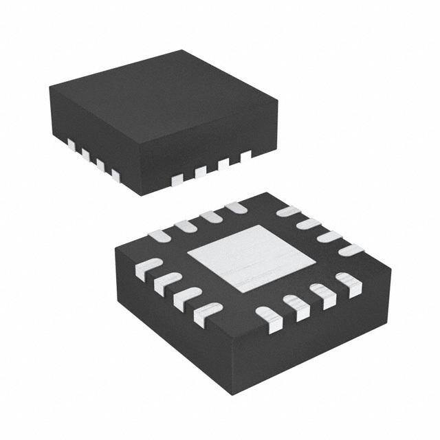
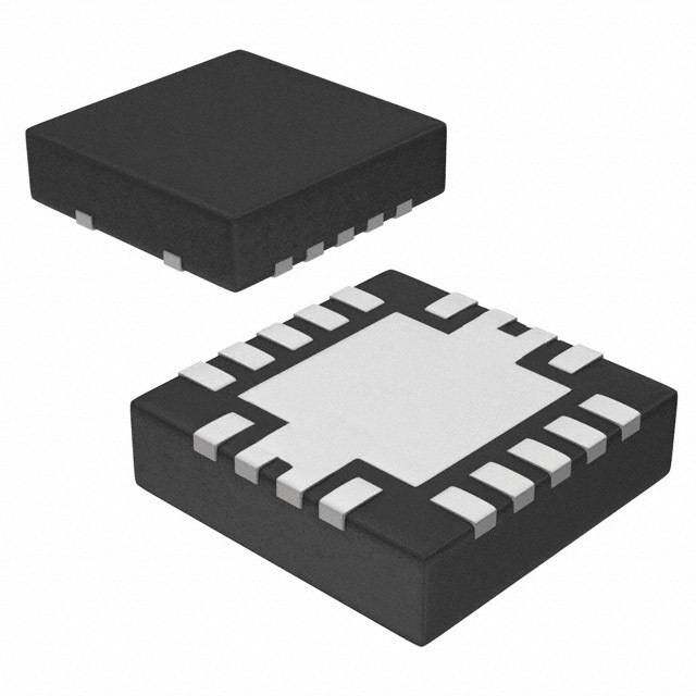
| 供应商器件封装 | 16-QFN(3x3) |
| 其它名称 | 296-28101-6 |
| 包装 | Digi-Reel® |
| 同步整流器 | 是 |
| 安装类型 | 表面贴装 |
| 封装/外壳 | 16-VFQFN 裸露焊盘 |
| 工作温度 | -40°C ~ 85°C |
| 标准包装 | 1 |
| 电压-输入 | 2.9 V ~ 6 V |
| 电压-输出 | 0.6 V ~ 5.04 V |
| 电流-输出 | 5A |
| 类型 | 降压(降压) |
| 输出数 | 1 |
| 输出类型 | 可调式 |
| 频率-开关 | 1.1MHz |

.jpg)


- 商务部:美国ITC正式对集成电路等产品启动337调查
- 曝三星4nm工艺存在良率问题 高通将骁龙8 Gen1或转产台积电
- 太阳诱电将投资9.5亿元在常州建新厂生产MLCC 预计2023年完工
- 英特尔发布欧洲新工厂建设计划 深化IDM 2.0 战略
- 台积电先进制程称霸业界 有大客户加持明年业绩稳了
- 达到5530亿美元!SIA预计今年全球半导体销售额将创下新高
- 英特尔拟将自动驾驶子公司Mobileye上市 估值或超500亿美元
- 三星加码芯片和SET,合并消费电子和移动部门,撤换高东真等 CEO
- 三星电子宣布重大人事变动 还合并消费电子和移动部门
- 海关总署:前11个月进口集成电路产品价值2.52万亿元 增长14.8%


PDF Datasheet 数据手册内容提取
Product Sample & Technical Tools & Support & Folder Buy Documents Software Community TPS53321 SLUSAF3A–DECEMBER2010–REVISEDNOVEMBER2016 TPS53321 5-A Step-Down Regulator With Integrated Switcher 1 Features 3 Description • 96%MaximumEfficiency The TPS53321 device provides a fully integrated 3-V 1 to 5-V V integrated synchronous FET converter • Continuous5-AOutputCurrent IN solution with 16 total components in 200 mm2 of PCB • SupportsAllMLCCOutputCapacitor area. Due to the low ON-resistance and TI's • SmoothPWM™Auto-SkipEco-Mode™forLight- Proprietary SmoothPWM™ skip mode of operation, it LoadEfficiency enables 96% peak efficiency and over 90% efficiency at loads as light as 100 mA. It requires only two 22- • OptimizedEfficiencyatLightandHeavyLoads µF ceramic output capacitors for a power dense 5-A • VoltageModeControl solution. • SupportsMaster-SlaveInterleavedOperation The TPS53321 features a 1.1-MHz switching • Synchronizationupto ±20%ofNominal frequency, skip mode operation support, prebias Frequency start-up, internal soft start, output soft discharge, • ConversionVoltageRangeBetween2.9Vand internal VBST switch, power good, EN/input UVLO, overcurrent, overvoltage, undervoltage, and 6V overtemperature protections, and all ceramic output • Soft-StopOutputDischargeDuringDisable capacitor support. It supports supply voltage from • AdjustableOutputVoltageRangingBetween 2.9 V to 3.5 V and conversion voltage from 2.9 V to 0.6Vand0.84V× V 6 V. The output voltage is adjustable from 0.6 V to IN 0.84V×V . • Overcurrent,Overvoltage,andOvertemperature IN Protection The TPS53321 is available in the 3 mm × 3 mm • Small3mm×3mm,16-PinQFNPackage 16-pin QFN package (Green RoHs compliant and Pb free)andoperatesbetween–40°Cand85°C. • Open-DrainPowerGoodIndication • InternalBootStrapSwitch DeviceInformation(1) • LowR ,24mΩWith3.3-VInputand19-mΩ DS(on) PARTNUMBER PACKAGE BODYSIZE(NOM) With5-VInput TPS53321 QFN(16) 3.00mm×3.00mm • SupportsPrebiasStart-Up (1) For all available packages, see the orderable addendum at theendofthedatasheet. 2 Applications • 5-VStep-DownRails • 3.3-VStep-DownRails TypicalApplicationCircuit OutputAllMLCCs V IN 2.9Vto6V 13 14 5 6 7 V VDD VIN VIN SW SW SW CBST IN 2.9Vto3.5V 12 VDD VBST 4 11 AGND TPS53321 PGD 3 PGD SYNC 2 SYNC FB 10 EN 1 EN 8 PS COMP 9 PGND PGND Pad 15 16 UDG-10204 Copyright © 2016,Texas Instruments Incorporated 1 An IMPORTANT NOTICE at the end of this data sheet addresses availability, warranty, changes, use in safety-critical applications, intellectualpropertymattersandotherimportantdisclaimers.PRODUCTIONDATA.
TPS53321 SLUSAF3A–DECEMBER2010–REVISEDNOVEMBER2016 www.ti.com Table of Contents 1 Features.................................................................. 1 7.4 DeviceFunctionalModes........................................11 2 Applications........................................................... 1 8 ApplicationandImplementation........................ 12 3 Description............................................................. 1 8.1 ApplicationInformation............................................12 4 RevisionHistory..................................................... 2 8.2 TypicalApplication..................................................12 5 PinConfigurationandFunctions......................... 3 9 PowerSupplyRecommendations...................... 18 6 Specifications......................................................... 4 10 Layout................................................................... 19 6.1 AbsoluteMaximumRatings......................................4 10.1 LayoutGuidelines.................................................19 6.2 ESDRatings..............................................................4 10.2 LayoutExample....................................................19 6.3 RecommendedOperatingConditions.......................4 11 DeviceandDocumentationSupport................. 20 6.4 ThermalInformation..................................................5 11.1 ReceivingNotificationofDocumentationUpdates20 6.5 ElectricalCharacteristics...........................................5 11.2 CommunityResources..........................................20 6.6 TypicalCharacteristics..............................................7 11.3 Trademarks...........................................................20 7 DetailedDescription.............................................. 9 11.4 ElectrostaticDischargeCaution............................20 7.1 Overview...................................................................9 11.5 Glossary................................................................20 7.2 FunctionalBlockDiagram.........................................9 12 Mechanical,Packaging,andOrderable Information........................................................... 20 7.3 FeatureDescription...................................................9 4 Revision History NOTE:Pagenumbersforpreviousrevisionsmaydifferfrompagenumbersinthecurrentversion. ChangesfromOriginal(December2010)toRevisionA Page • AddedESDRatingstable,FeatureDescriptionsection,DeviceFunctionalModes,ApplicationandImplementation section,PowerSupplyRecommendationssection,Layoutsection,DeviceandDocumentationSupportsection,and Mechanical,Packaging,andOrderableInformationsection.................................................................................................. 1 • DeletedOrderingInformationtable;seePOAattheendofthedatasheet........................................................................... 1 • DeletedLeadtemperature,1.6mm(1/16inch)fromcasefor10seconds:300°C................................................................ 4 • DeletedPackageDissipationRatingstable............................................................................................................................ 5 • AddedThermalInformationtable........................................................................................................................................... 5 • ChangedR2valueinTypical3.3-VInputApplicationCircuitDiagramFrom:4.02kΩTo:2.67kΩ.................................... 12 • ChangedR2valueinMasterandSlaveConfigurationSchematicFrom:4.02kΩTo:2.67kΩ.......................................... 16 • ChangedR12valueinMasterandSlaveConfigurationSchematicFrom:2.67kΩTo:4.02kΩ........................................ 16 2 SubmitDocumentationFeedback Copyright©2010–2016,TexasInstrumentsIncorporated ProductFolderLinks:TPS53321
TPS53321 www.ti.com SLUSAF3A–DECEMBER2010–REVISEDNOVEMBER2016 5 Pin Configuration and Functions RGTPackage 16-PinQFN TopView D D N N G G N N P P VI VI 6 5 4 3 1 1 1 1 EN 1 12 VDD SYNC 2 11 AGND Thermal PGD 3 Pad 10 FB VBST 4 9 COMP 5 6 7 8 W W W S Not to scale S S S P PinFunctions PIN TYPE(1) DESCRIPTION NO. NAME 1 EN I Enable.InternallypulleduptoVDDwitha1.35-MΩresistor. Synchronizationsignalforinputinterleaving.MasterSYNCpinsendsout180°out-of-phasesignalto 2 SYNC B slaveSYNC.SYNCfrequencymustbewithin±20%ofslavenominalfrequency. 3 PGD O Powergoodoutputflag.Open-drainoutput.Pulluptoanexternalrailthrougharesistor. Supplyinputforhigh-sideMOSFET(bootstrapterminal).ConnectcapacitorfromthispintoSW 4 VBST P terminal. 5 SW B Outputinductorconnectiontointegratedpowerdevices 6 SW B Outputinductorconnectiontointegratedpowerdevices 7 SW B Outputinductorconnectiontointegratedpowerdevices Modeconfigurationpin(with10-µAcurrent): Connectingtoground:FCCMslave Pulledhighorfloating(internalpulledhigh):FCCMmaster 8 PS I Connecta24.3-kΩresistortoGND:DEslave Connecta57.6-kΩresistortoGND:HEFmode Connecta105-kΩresistortoGND:reservedmode Connecta174-kΩresistortoGND:DEmaster 9 COMP O Erroramplifiercompensationterminal.TypeIIIcompensationmethodisrecommendedforstability. 10 FB I Voltagefeedback.AlsousedforOVP,UVP,andPGDdetermination. 11 AGND G Deviceanaloggroundterminal 12 VDD P Inputbiassupplyforanalogfunctions 13 VIN P Gatedriversupplyandpowerconversionvoltageinput 14 VIN P Gatedriversupplyandpowerconversionvoltageinput 15 PGND P ICpowerGNDterminal 16 PGND P ICpowerGNDterminal (1) B=Bidirectional,G=Ground,I=Input,O=Output,P=Supply Copyright©2010–2016,TexasInstrumentsIncorporated SubmitDocumentationFeedback 3 ProductFolderLinks:TPS53321
TPS53321 SLUSAF3A–DECEMBER2010–REVISEDNOVEMBER2016 www.ti.com 6 Specifications 6.1 Absolute Maximum Ratings overoperatingfree-airtemperaturerange(unlessotherwisenoted)(1) MIN MAX UNIT VIN,EN –0.3 7 VBST –0.3 17 Inputvoltage V VBST(withrespecttoSW) –0.3 7 FB,PS,VDD –0.3 3.7 DC –0.3 7 SW Pulse<20ns,E=5µJ –3 10 Outputvoltage PGD –0.3 7 V COMP,SYNC –0.3 3.7 PGND –0.3 0.3 Junctiontemperature,T –40 150 °C J Ambienttemperature,T –40 85 °C A Storagetemperature,T –55 150 °C stg (1) StressesbeyondthoselistedunderAbsoluteMaximumRatingsmaycausepermanentdamagetothedevice.Thesearestressratings only,whichdonotimplyfunctionaloperationofthedeviceattheseoranyotherconditionsbeyondthoseindicatedunderRecommended OperatingConditions.Exposuretoabsolute-maximum-ratedconditionsforextendedperiodsmayaffectdevicereliability. 6.2 ESD Ratings VALUE UNIT Human-bodymodel(HBM),perANSI/ESDA/JEDECJS-001(1) ±2000 V Electrostaticdischarge V (ESD) Charged-devicemodel(CDM),perJEDECspecificationJESD22-C101(2) ±500 (1) JEDECdocumentJEP155statesthat500-VHBMallowssafemanufacturingwithastandardESDcontrolprocess. (2) JEDECdocumentJEP157statesthat250-VCDMallowssafemanufacturingwithastandardESDcontrolprocess. 6.3 Recommended Operating Conditions MIN NOM MAX UNIT VIN 2.9 6 VDD 2.9 3.3 3.5 VBST –0.1 13.5 Inputvoltage V VBST(withrespecttoSW) –0.1 6 EN –0.1 6 FB,PS –0.1 3.5 SW –1 6.5 PGD –0.1 6 Outputvoltage V COMP,SYNC –0.1 3.5 PGND –0.1 0.1 T Junctiontemperature –40 125 °C J 4 SubmitDocumentationFeedback Copyright©2010–2016,TexasInstrumentsIncorporated ProductFolderLinks:TPS53321
TPS53321 www.ti.com SLUSAF3A–DECEMBER2010–REVISEDNOVEMBER2016 6.4 Thermal Information TPS53321 THERMALMETRIC(1) RGT(QFN) UNIT 16PINS R Junction-to-ambientthermalresistance 42.8 °C/W θJA R Junction-to-case(top)thermalresistance 51.3 °C/W θJC(top) R Junction-to-boardthermalresistance 16 °C/W θJB ψ Junction-to-topcharacterizationparameter 0.7 °C/W JT ψ Junction-to-boardcharacterizationparameter 16 °C/W JB R Junction-to-case(bottom)thermalresistance 4.4 °C/W θJC(bot) (1) Formoreinformationabouttraditionalandnewthermalmetrics,seetheSemiconductorandICPackageThermalMetricsapplication report. 6.5 Electrical Characteristics overrecommendedfree-airtemperaturerange,V =3.3V,V =3.3V,andPGND=GND(unlessotherwisenoted) IN VDD PARAMETER TESTCONDITIONS MIN TYP MAX UNIT SUPPLY:VOLTAGE,CURRENTS,andUVLO V VINsupplyvoltage Nominalinputvoltagerange 2.9 6 V IN I VINshutdowncurrent EN=LO 3 µA VINSDN V VINUVLOthreshold Rampup,EN=HI 2.8 V UVLO V VINUVLOhysteresis VINUVLOHysteresis 130 mV UVLOHYS V Internalcircuitrysupplyvoltage Nominal3.3-Vinputvoltagerange 2.9 3.3 3.5 V DD I VDDshutdowncurrent EN=LO 5 µA DDSDN I Standbycurrent EN=HI,noswitching 2.2 3.5 mA DD V 3.3-VUVLOthreshold Rampup,EN=HI 2.8 V DDUVLO V 3.3-VUVLOhysteresis 75 mV DDUVLOHYS VOLTAGEFEEDBACKLOOP:VREFANDERRORAMPLIFIER V VREF Internalprecisionreferencevoltage 0.6 V VREF 0°C≤T ≤85°C –1% 1% A TOLV VREFTolerance REF –40°C≤T ≤85°C –1.25% 1.25% A UGBW(1) Unitygainbandwidth 14 MHz A (1) Open-loopgain 80 dB OL I FBinputleakagecurrent SourcedfromFBpin 30 nA FBINT I (1) Outputsinkingandsourcing C =20pF 5 mA EAMAX current COMP SR(1) Slewrate 5 V/µs OCP:OVERCURRENTANDZEROCROSSING WhenI exceedsthisthresholdfor4 OUT I OvercurrentlimitonupperFET consecutivecycles.V =3.3V, 6 6.5 7 A OCPL IN V =1.5Vwith1-µHinductor,T =25°C OUT A Immediatelyshutsdownwhensensedcurrent Onetimeovercurrentlatchoff I reachthisvalue.V =3.3V, 6.25 6.8 7.35 A OCPH onthelowerFET IN V =1.5Vwith1-µHinductor,T =25°C OUT A t Hiccuptimeinterval 12.5 14.5 16.5 ms HICCUP V (1) Zerocrossingcomparator PGND–SW,skipmode –4.5 –3 –1.5 mV ZXOFF internaloffset PROTECTION:OVP,UVP,PGD,ANDINTERNALTHERMALSHUTDOWN Overvoltageprotection V MeasuredatFBw/r/tVREF 114% 117% 120% OVP thresholdvoltage Undervoltageprotection V MeasuredatFBw/r/tVREF 80% 83% 86% UVP thresholdvoltage (1) Ensuredbydesign.Notproductiontested. Copyright©2010–2016,TexasInstrumentsIncorporated SubmitDocumentationFeedback 5 ProductFolderLinks:TPS53321
TPS53321 SLUSAF3A–DECEMBER2010–REVISEDNOVEMBER2016 www.ti.com Electrical Characteristics (continued) overrecommendedfree-airtemperaturerange,V =3.3V,V =3.3V,andPGND=GND(unlessotherwisenoted) IN VDD PARAMETER TESTCONDITIONS MIN TYP MAX UNIT V PGDlowthreshold MeasuredatFBw/r/tVREF 80% 83% 86% PGDL V PGDupperthreshold MeasuredatFBw/r/tVREF 114% 117% 120% PGDU MinimumVinvoltageforvalid MeasuredatV with1-mA(or2-mA)sink V IN 1 V INMINPG PGDatstart-up currentonPGDpinatstart-up THSD(1) Thermalshutdown Latchoffcontroller,attemptsoft-stop 130 140 150 °C THSD (1) Thermalshutdownhysteresis Controllerrestartsaftertemperaturehasdropped 40 °C HYS LOGICPINS:I/OVOLTAGEANDCURRENT V PGDpulldownvoltage Pulldownvoltagewith4-mAsinkcurrent 0.2 0.4 V PGPD I PGDleakagecurrent Hi-Zleakagecurrent,apply3.3-Vinoffstate –2 0 2 µA PGLK R Enablepullupresistor 1.35 MΩ ENPU V ENlogichighthreshold 1.1 1.18 1.3 V ENH V ENhysteresis 0.18 0.24 V ENHYS Level1tolevel2(2) 0.12 Level2tolevel3 0.4 PS PSmodethresholdvoltage Level3tolevel4 0.8 V THS Level4tolevel5 1.4 Level5tolevel6 2.2 I PSsource 10-µApullupcurrentwhenenabled 8 10 12 µA PS f SlaveSYNCfrequencyrange Versusnominalswitchingfrequency –20% 20% SYNCSL PW SYNClowpulsewidth 110 ns SYNC I SYNCpinsinkcurrent T =25°C 10 µA SYNC A V (1) SYNCthreshold Fallingedge 1 V SYNCTHS V (1) SYNChysteresis 0.5 V SYNCHYS BOOTSTRAP:VOLTAGEANDLEAKAGECURRENT I VBSTleakagecurrent V =3.3V,V =6.6V,T =25°C 1 µA VBSTLK IN VBST A TIMERS:SS,FREQUENCY,RAMP,ON-TIMEANDI/OTIMING t DelayafterENasserting EN=HI,masterorHEFmode 0.2 ms SS_1 t DelayafterENasserting EN=HI,slavewaitingtime 0.5 ms SS_2 t Soft-startramp-uptime RisingfromV =0VtoV =0.6V 0.4 ms SS_3 SS SS RisingfromV =0VtoV =0.6V, t PGDstart-updelaytime SS SS 1.2 ms PGDENDLY fromV reaching0.6VtoV goinghigh SS PGD Overvoltageprotectiondelay t TimefromFBoutof+20%ofVREFtoOVPfault 1 1.7 2.5 µs OVPDLY time Undervoltageprotectiondelay t TimefromFBoutof–20%ofVREFtoUVPfault 11 µs UVPDLY time f Switchingfrequencycontrol FCCM 0.99 1.1 1.21 MHz SW Rampamplitude(1) 2.9V<V <6.0V V /4 V IN IN FCCMorDEmode 100 140 t MinimumOFFtime ns MIN(off) HEFmode 175 250 Maximumdutycycle,FCCM f =1.1MHz,0°C≤T ≤85°C 84% 89% andDEmode SW A D MAX Maximumdutycycle,HEF f =1.1MHz,0°C≤T ≤85°C 75% 81% mode SW A Soft-dischargetransistor R V =Low,V =3.3V,V =0.5V 60 Ω SFTSTP resistance EN IN OUT (2) SeePSpindescriptionforlevels. 6 SubmitDocumentationFeedback Copyright©2010–2016,TexasInstrumentsIncorporated ProductFolderLinks:TPS53321
TPS53321 www.ti.com SLUSAF3A–DECEMBER2010–REVISEDNOVEMBER2016 6.6 Typical Characteristics InductorPCMC065T-1R0(1µH,5.6mΩ)isused. 100 100 95 95 90 90 %) %) y ( y ( nc 85 nc 85 e e ci ci Effi 80 VOUT = 1.0 V Effi 80 VOUT = 1.0 V VOUT = 1.2 V VOUT = 1.2 V 75 VOUT = 1.5 V 75 VOUT = 1.5 V VOUT = 1.8 V Skip Mode VOUT = 1.8 V FCCM VOUT = 2.5 V VIN = 3.3 V VOUT = 2.5 V VIN = 3.3 V 70 70 0.0 0.5 1.0 1.5 2.0 2.5 3.0 3.5 4.0 4.5 5.0 0.0 0.5 1.0 1.5 2.0 2.5 3.0 3.5 4.0 4.5 5.0 Output Current (A) Output Current (A) Figure1.EfficiencyvsOutputCurrent, Figure2.EfficiencyvsOutputCurrent, SkipMode,V =3.3V FCCM,V =3.3V IN IN 100 100 95 95 90 90 %) %) y ( y ( nc 85 nc 85 e e ci ci Effi 80 VVOOUUTT == 11..02 VV Effi 80 VVOOUUTT == 11..02 VV VOUT = 1.5 V VOUT = 1.5 V 75 VOUT = 1.8 V 75 VOUT = 1.8 V VOUT = 2.5 V Skip Mode VOUT = 2.5 V FCCM VOUT = 3.3 V VIN = 5 V VOUT = 3.3 V VIN = 5 V 70 70 0.0 0.5 1.0 1.5 2.0 2.5 3.0 3.5 4.0 4.5 5.0 0.0 0.5 1.0 1.5 2.0 2.5 3.0 3.5 4.0 4.5 5.0 Output Current (A) Output Current (A) Figure3.EfficiencyvsOutputCurrent, Figure4.EfficiencyvsOutputCurrent, SkipMode,V =5V FCCM,V =5V IN IN 0.620 0.5 0.615 %) 0.3 V) 0.610 e ( age ( 0.605 hang 0.1 Volt 0.600 e C Feedback 00..559905 utput Voltag −0.1 O −0.3 0.585 VIN = 3.3 V VIN = 5.0 V 0.580 −0.5 −40 −25 −10 5 20 35 50 65 80 95 110 125 0.0 0.5 1.0 1.5 2.0 2.5 3.0 3.5 4.0 4.5 5.0 Temperature (°C) Output Current (A) Figure5.FeedbackVoltagevsAmbientTemperature Figure6.OutputVoltageChangevsOutputCurrent Copyright©2010–2016,TexasInstrumentsIncorporated SubmitDocumentationFeedback 7 ProductFolderLinks:TPS53321
TPS53321 SLUSAF3A–DECEMBER2010–REVISEDNOVEMBER2016 www.ti.com Typical Characteristics (continued) InductorPCMC065T-1R0(1µH,5.6mΩ)isused. 10000 10000 VIN = 3.3 V VIN = 5.0 V z) 1000 z) 1000 H H k k y ( y ( c c n n e e u u q q e e Fr 100 Fr 100 FCCM FCCM HEF Mode HEF Mode DE Mode DE Mode 10 10 0.01 0.1 1 10 0.01 0.1 1 10 Output Current (A) Output Current (A) Figure7.FrequencyvsOutputCurrent Figure8.FrequencyvsOutputCurrent atV =3.3V atV =5V IN IN HEFMode HEFMode EN(5V/div) EN(5V/div) V =3.3V V =3.3V IN IN I =0A I =0A OUT OUT V (1V/div) 0.5Vpre-biased V (1V/div) OUT OUT PGD(5V/div) PGD(5V/div) t–Time–200ms/div t–Time–200ms/div Figure9.NormalStart-UpWaveform Figure10.PrebiasStart-UpWaveform 90 80 EN(5V/div) HEFMode 70 C) NoAirFlow VIN=3.3V (° e 60 IOUT=0A atur er 50 p VOUT(1V/div) Tem 3400 VVVVVINOOOOUUUU=TTTT3====.30112....V6285@VVVV VVVVVVOOOOOINUUUUUTTTTT======501123V.....62853@VVVVV 20 PGD(5V/div) 0.0 0.5 1.0 1.5 2.0 2.5 3.0 3.5 4.0 4.5 5.0 OutputCurrent(A) t–Time–4ms/div Figure11.Soft-StopWaveform Figure12.SafeOperatingArea 8 SubmitDocumentationFeedback Copyright©2010–2016,TexasInstrumentsIncorporated ProductFolderLinks:TPS53321
TPS53321 www.ti.com SLUSAF3A–DECEMBER2010–REVISEDNOVEMBER2016 7 Detailed Description 7.1 Overview The TPS53321 is a high-efficiency switching regulator with two integrated N-channel MOSFETs and is capable ofdeliveringupto5Aofloadcurrent.TheTPS53321providesoutputvoltagebetween0.6Vand0.84 ×V from IN 2.9Vto6Vwideinputvoltagerange. This device employs five operation modes to fit various application requirements. The master or slave mode enables a two-phase interleaved operation to reduce input ripple. The skip mode operation provides reduced power loss and increases the efficiency at light load. The unique, patented PWM modulator enables smooth light loadtoheavyloadtransitionwhilemaintainingfastloadtransient. 7.2 Functional Block Diagram VIN VIN 14 13 4 VBST 0.6V–17% 0.6V UV/OV + Threshold UV VINUVLO Generation FB 10 + 5 SW 0.6V+17% OV Control HDRV Logic 6 SW PWM 7 SW + COMP 9 E/A+ 0.6V Ramp XCON + PWM LLOne-Shot SS Overtemp LDRV V Discharge 15 PGND OUT 16 PGND Enable Mode OCPLogic OSC Control Scanner VDDUVLO 12 VDD TPS53321 2 1 8 3 11 SYNC EN PS PGD AGND UDG-10205 Copyright © 2016,Texas Instruments Incorporated 7.3 Feature Description 7.3.1 SoftStart The soft-start function reduces the inrush current during the start up sequence. A slow-rising reference voltage is generated by the soft-start circuitry and sent to the input of the error amplifier. When the soft-start ramp voltage is less than 600 mV, the error amplifier uses this ramp voltage as the reference. When the ramp voltage reaches 600mV,theerroramplifierswitchestoafixed600-mVreference.Thetypicalsoft-starttimeis400 µs. 7.3.2 PowerGood The TPS53321 monitors the voltage on the FB pin. If the FB voltage is between 83% and 117% of the reference voltage,thepowergoodsignalremainshigh.IftheFBvoltagefallsoutsideoftheselimits,theinternalopen-drain outputpullsthepowergoodpin(PGD)low. Copyright©2010–2016,TexasInstrumentsIncorporated SubmitDocumentationFeedback 9 ProductFolderLinks:TPS53321
TPS53321 SLUSAF3A–DECEMBER2010–REVISEDNOVEMBER2016 www.ti.com Feature Description (continued) During start-up, V must be higher than 1 V to have valid power good logic, and the power good signal is IN delayed for 1.2 ms after the FB voltage falls to within the power good limits. There is also 10-µs delay during the shutdownsequence. 7.3.3 UndervoltageLockout(UVLO)Protection The TPS53321 provides undervoltage lockout (UVLO) protection for both power input (V ) and bias input (VDD) IN voltage. If either of them is lower than the UVLO threshold voltage minus the hysteresis, the device shuts off. When the voltage rises above the threshold voltage, the device restarts. The typical UVLO rising threshold is 2.8 V for both V and V . A hysteresis voltage of 130 mV for V and 75 mV for V is also provided to IN VDD IN VDD preventglitch. 7.3.4 OvercurrentProtection The TPS53321 continuously monitors the current flowing through the high-side and the low-side MOSFETs. If the current through the high-side FET exceeds 6.5 A, the high-side FET turns off and the low-side FET turns on until the next PWM cycle. An overcurrent (OC) counter starts to increment each occurrence of an overcurrent event. The converter shuts down immediately when the OC counter reaches four. The OC counter resets if the detectedcurrentisless6.5AafteranOCevent. Another set of overcurrent circuitry monitors the current flowing through low-side FET. If the current through the low-side FET exceeds 6.8 A, the overcurrent protection is enabled and immediately turns off both the high-side and the low-side FETs and shuts down the converter. The device is fully protected against overcurrent during both on-time and off-time. The device attempts to restart after a hiccup delay of 14.5 ms (typical). If the overcurrentconditionclearsbeforerestart,thedevicestartsupnormally. 7.3.5 OvervoltageProtection The TPS53321 monitors the voltage divided feedback voltage to detect overvoltage and undervoltage conditions. When the feedback voltage is greater than 117% of the reference, the high-side MOSFET turns off and the low- side MOSFET turns on. The output voltage then drops until it reaches the undervoltage threshold. At that point thelow-sideMOSFETturnsoffandthedeviceentersahigh-impedancestate. 7.3.6 UndervoltageProtection When the feedback voltage is lower than 83% of the reference voltage, the undervoltage protection timer starts. If the feedback voltage remains lower than the undervoltage threshold voltage after 10 µs, the device turns off both the high-side and the low-side MOSFETs and goes into a high-impedance state. The device attempts to restartafterahiccupdelayof14.5ms(typical). 7.3.7 OvertemperatureProtection The TPS53321 continuously monitors the die temperature. If the die temperature exceeds the threshold value (140˚C typical), the device shuts off. When the device temperature falls to 40˚C below the overtemperature threshold,itrestartsandreturnstonormaloperation. 7.3.8 OutputDischarge When the enable pin is low, the TPS53321 discharges the output capacitors through an internal MOSFET switch between SW and PGND while high-side and low-side MOSFETs remain off. The typical discharge switch ON- resistanceis60Ω.ThisfunctionisdisabledwhenV islessthan1V. IN 7.3.9 MasterandSlaveOperationandSynchronization Two TPS53321 can operate interleaved when configured as master and slave. The SYNC pins of the two devices are connected together for synchronization. In CCM, the master device sends the 180° out-of-phase pulse to the slave device through the SYNC pin, which determines the leading edge of the PWM pulse. If the slave device does not receive the SYNC pulse from the master device or if the SYNC connection is broken duringoperation,theslavedevicecontinuestooperateusingitsowninternalclock. 10 SubmitDocumentationFeedback Copyright©2010–2016,TexasInstrumentsIncorporated ProductFolderLinks:TPS53321
TPS53321 www.ti.com SLUSAF3A–DECEMBER2010–REVISEDNOVEMBER2016 Feature Description (continued) In DE mode, the master and slave switching node does not synchronize to each other if either one of them is operating in DCM. When both master and slave enter CCM, the switching nodes of the master and the slave synchronizetoeachother. The SYNC pin of the slave device can also connect to external clock source within ±20% of the 1.1-MHz switchingfrequency.ThefallingedgeoftheSYNCtriggerstherisingedgeofthePWMsignal. 7.4 Device Functional Modes 7.4.1 OperationModes TheTPS53321offersfiveoperationmodesdeterminedbythePSpinconnectionslistedinTable1. Table1.OperationModeSelection PSPINCONNECTION OPERATIONMODE AUTO-SKIPATLIGHTLOAD MASTER/SLAVESUPPORT GND FCCMSlave — Slave 24.3kΩtoGND DESlave Yes Slave 57.6kΩtoGND HEFMode Yes — 174kΩtoGND DEMaster Yes Master FloatingorpulledtoVDD FCCMMaster — Master Inforcedcontinuousconduction mode(FCCM),thehigh-sideFETisONduringtheon-timeandthelow-sideFET is ON during the off-time. The switching is synchronized to the internal clock thus the switching frequency is fixed. In diode emulation (DE) mode, the high-side FET is ON during the on-time and low-side FET is ON during the off-time until the inductor current reaches zero. An internal zero-crossing comparator detects the zero crossing of inductor current from positive to negative. When the inductor current reaches zero, the comparator sends a signaltothelogiccontrolandturnsoffthelow-sideFET. When the load is increased, the inductor current is always positive and the zero-crossing comparator does not send a zero-crossing signal. The converter enters into continuous conduction mode (CCM) when no zero- crossing is detected for two consecutive PWM pulses. The switching synchronizes to the internal clock and the switchingfrequencyisfixed. In high-efficiency (HEF) mode, the operation is the same as DE mode at light load. However, the converter does not synchronize to the internal clock during CCM. Instead, the PWM modulator determines the switching frequency. 7.4.2 Eco-Mode™Light-LoadOperation In skip modes (DE and HEF) when the load current is less than one-half of the inductor peak current, the inductor current becomes negative by the end of off-time. During light load operation, the low-side MOSFET is turned off when the inductor current reaches zero. The energy delivered to the load per switching cycle is increased compared to the normal PWM mode operation and the switching frequency is reduced. The switching lossisreduced,therebyimprovingefficiency. In both DE and HEF mode, the switching frequency is reduced in discontinuous conduction mode (DCM). When the load current is 0 A, the minimum switching frequency is reached. The difference between V and V VBST SW mustbemaintainedatavaluehigherthan2.4V. 7.4.3 ForcedContinuousConductionMode(FCCM) When the PS pin is grounded or greater than 2.2 V, the TPS53321 is operating in forced continuous conduction mode in both light-load and heavy-load conditions. In this mode, the switching frequency remains constant over the entire load range, making it suitable for applications that require tight control of switching frequency at a cost oflowerefficiencyatlightload. Copyright©2010–2016,TexasInstrumentsIncorporated SubmitDocumentationFeedback 11 ProductFolderLinks:TPS53321
TPS53321 SLUSAF3A–DECEMBER2010–REVISEDNOVEMBER2016 www.ti.com 8 Application and Implementation NOTE Information in the following applications sections is not part of the TI component specification, and TI does not warrant its accuracy or completeness. TI’s customers are responsible for determining suitability of components for their purposes. Customers should validateandtesttheirdesignimplementationtoconfirmsystemfunctionality. 8.1 Application Information The TPS53321 device is a high-efficiency synchronous-buck converter. The device suits low output voltage point-of-loadapplicationswith5-Aorloweroutputcurrentincomputingandsimilardigitalconsumerapplications. 8.2 Typical Application This design example describes a voltage-mode, 5-A synchronous buck converter with integrated MOSFETs. The deviceprovidesafixed1.5-Voutputatupto5Afroma3.3-Vinputbus. L1 1mH OutputallMLCCs VIN C5 C6 R6 COUT 22mF 0.1mF 2.2W 3x22mF 13 14 5 6 7 C4 1Cm8F VIN VIN SW SW SW 0.1mF VIN 12 VDD VBST 4 R7 11 AGND 20kW R3 C1 TPS53321 PGD 3 PGD 20W 2.2nF SYNC 2 SYNC FB 10 R4 EN 1 EN R1 R5 C2 2.2nF 4.02kW 8 PS PGND PGND COMP 9 4.02kW 57.6kW 15 16 C3 R2 100pF 2.67kW UDG-10206 Copyright © 2016,Texas Instruments Incorporated Figure13. Typical3.3-VInputApplicationCircuitDiagram 8.2.1 DesignRequirements Table2liststhedesignspecificationsforthisapplicationexample. Table2.TPS53321DesignExampleSpecifications PARAMETER TESTCONDITIONS MIN TYP MAX UNIT INPUTCHARACTERISTICS Inputvoltage,VIN Vin 2.9 3.3 6 V Maximuminputcurrent Vin=3.3V,1.5V/5A 2.67 A Noloadinputcurrent Vin=3.3V,1.5V/0A 12.5 mA 12 SubmitDocumentationFeedback Copyright©2010–2016,TexasInstrumentsIncorporated ProductFolderLinks:TPS53321
TPS53321 www.ti.com SLUSAF3A–DECEMBER2010–REVISEDNOVEMBER2016 Typical Application (continued) Table2.TPS53321DesignExampleSpecifications(continued) PARAMETER TESTCONDITIONS MIN TYP MAX UNIT OUTPUTCHARACTERISTICS Outputvoltage,Vo 1.485 1.5 1.515 V Lineregulation 0.1% Outputvoltageregulation Loadregulation 1% Outputvoltageripple Vin=3.3V,1.5V/0Ato5A 20 mVpp Outputloadcurrent 0 5 A Outputovercurrent 6.5 A OUTPUTCHARACTERISTICS Switchingfrequency Fixed 1.1 MHz Vin=3.3V,1.5V/5A 85.94% 1.5-Vfullloadefficiency Vin=5V,1.5V/5A 87% Operatingtemperature 25 °C 8.2.2 DetailedDesignProcedure 8.2.2.1 DeterminetheValueofR1andR2 The output voltage is programmed by the voltage-divider resistor, R1 and R2 shown in Figure 13. R1 is connected between the FB pin and the output, and R2 is connected between the FB pin and GND. The recommendedvalueforR1isfrom1kΩto5kΩ.DetermineR2usingequationinEquation1. 0.6 R2= ´R1 V -0.6 OUT (1) 8.2.2.2 ChoosetheInductor The inductance value must be determined to give the ripple current of approximately 20% to 40% of maximum outputcurrent.TheinductorripplecurrentisdeterminedbyEquation2. 1 (VIN-VOUT)´VOUT I = ´ L(ripple) L´f V SW IN (2) The inductor also requires low DCR to achieve good efficiency, as well as enough room above peak inductor currentbeforesaturation. 8.2.2.3 ChoosetheOutputCapacitor(s) The output capacitor selection is determined by output ripple and transient requirement. When operating in CC mode,theoutputripplehasthreecomponentscalculatedwithEquation3 throughEquation6. VRIPPLE = VRIPPLE(C)+VRIPPLE(ESR)+VRIPPLE(ESL) (3) I L(ripple) V = RIPPLE(C) 8´C ´f OUT SW (4) V =I ´ESR RIPPLE(ESR) L(ripple) (5) V = VIN´ESL RIPPLE(ESL) L (6) When ceramic output capacitors are used, the ESL component is usually negligible. In the case when multiple output capacitors are used, ESR and ESL must be the equivalent of ESR and ESL of all the output capacitor in parallel. When operating in DCM, the output ripple is dominated by the component determined by capacitance. It also varieswithloadcurrentandcanbeexpressedasshowninEquation7. Copyright©2010–2016,TexasInstrumentsIncorporated SubmitDocumentationFeedback 13 ProductFolderLinks:TPS53321
TPS53321 SLUSAF3A–DECEMBER2010–REVISEDNOVEMBER2016 www.ti.com ( )2 a´I -I L(ripple) OUT V = RIPPLE(DCM) 2´C ´f ´I OUT SW L(ripple) where • αistheDCMon-timecoefficientandcanbeexpressedinEquation8(typicalvalue1.25) (7) t ON(DCM) a = t ON(CCM) (8) I L V OUT axI L(ripple) V RIPPLE I OUT T1 axT UDG-10055 Figure14. DCMV RippleCalculation OUT 8.2.2.4 ChoosetheInputCapacitor The selection of input capacitor must be determined by the ripple current requirement. The ripple current generated by the converter must be absorbed by the input capacitors as well as the input source. The RMS ripplecurrentfromtheconvertercanbeexpressedinEquation9. I =I ´ D´(1-D) IN(ripple) OUT where • DisthedutycycleandcanbeexpressedasshowninEquation10 (9) V D= OUT V IN (10) To minimize the ripple current drawn from the input source, sufficient input decoupling capacitors must be placed closetothedevice.TheceramiccapacitorisrecommendedbecauseitprovideslowESRandlowESL.Theinput voltageripplecanbecalculatedasshowninEquation11whenthetotalinputcapacitanceisdetermined. I ´D V = OUT IN(ripple) f ´C SW IN (11) 8.2.2.5 CompensationDesign The TPS53321 uses voltage mode control. To effectively compensate the power stage and ensure fast transient response,TypeIIIcompensationistypicallyused. ThecontroltooutputtransferfunctioncanbedescribedinEquation12. 14 SubmitDocumentationFeedback Copyright©2010–2016,TexasInstrumentsIncorporated ProductFolderLinks:TPS53321
TPS53321 www.ti.com SLUSAF3A–DECEMBER2010–REVISEDNOVEMBER2016 1+s´C ´ESR G =4´ OUT CO æ L ö 1+s´ç +C ´(ESR+DCR)÷+s2´L´C èDCR+RLOAD OUT ø OUT (12) TheoutputL-CfilterintroducesadoublepolewhichcanbecalculatedasshowninEquation13. 1 f = DP 2´p´ L´C OUT (13) TheESRzerocanbecalculatedasshowninEquation14. 1 f = ESR 2´p´ESR´C OUT (14) Figure 15 and Figure 16 show the configuration of Type III compensation and typical pole and zero locations. Equation 16 through Equation 20 describe the compensator transfer function and poles and zeros of the Type III network. C3 C1 R4 C2 R1 R3 B) d ( n ai COMP G VREF + R2 UGD-10058 f f f f Z1 Z2 P2 P3 Frequency UDG-10057 Figure15. TypeIIICompensationNetwork Figure16. TypeIIICompensationGainPlotand ConfigurationSchematic Zero/PolePlacement (1+s´C ´(R +R ))(1+s´R ´C ) 1 1 3 4 2 G = EA æ C ´C ö (s´R1´(C2 +C3))´(1+s´C1´R3)´ç1+s´R4 2 3 ÷ C +C è 2 3 ø (15) 1 f = Z1 2´p´R ´C 4 2 (16) 1 1 f = @ Z2 2´p´(R +R )´C 2´p´R ´C 1 3 1 1 1 (17) f =0 P1 (18) 1 f = P2 2´p´R ´C 3 1 (19) 1 1 f = @ P3 æC ´C ö 2´p´R ´C 2´p´R4´çC2+C3 ÷ 4 3 è 2 3 ø (20) Copyright©2010–2016,TexasInstrumentsIncorporated SubmitDocumentationFeedback 15 ProductFolderLinks:TPS53321
TPS53321 SLUSAF3A–DECEMBER2010–REVISEDNOVEMBER2016 www.ti.com The two zeros can be placed near the double pole frequency to cancel the response from the double pole. One pole can be used to cancel ESR zero, and the other non-zero pole can be placed at half switching frequency to attenuate the high frequency noise and switching ripple. Suitable values can be selected to achieve a compromise between high phase margin and fast response. A phase margin higher than 45 degrees is required forstableoperation. For DCM operation, a C3 between 56 pF and 150 pF is recommended for output capacitance between 20 µF to 200µF. Figure17showsthemasterandslaveconfigurationschematicforadesignwitha3.3-Vinput. L1 1mH VIN OutputallMLCCs VOUT=1.2V 3.3V C5 C6 R6 COUT 22mF 0.1mF 2.2W 3x22mF 13 14 5 6 7 C4 1Cm8F VIN VIN SW SW SW 0.1mF VIN 12 VDD VBST 4 R7 11 AGND 20kW PGD_Master R3 C1 TPS53321 PGD 3 20W 2.2nF 2 SYNC EN_Master 1 EN FB 10 R4 R1 C2 2.2nF 4.02kW 8 PS PGND PGND COMP 9 4.02kW 15 16 C3 R2 100pF 2.67kW L11 1mH VIN OutputallMLCCs VOUT=1.5V C15 C16 R16 COUT 22mF 0.1mF 2.2W 3x22mF 13 14 5 6 7 C14 1C1m8F VIN VIN SW SW SW 0.1mF VIN 12 VDD VBST 4 R17 11 AGND 20kW PGD_Master R13 C11 TPS53321 PGD 3 20W 2.2nF 2 SYNC EN_Slave 1 EN FB 10 R14 R11 C12 2.2nF 4.02kW 8 PS PGND PGND COMP 9 4.02kW 15 16 C13 R12 100pF 4.02kW UDG-10207 Copyright © 2016,Texas Instruments Incorporated Figure17. MasterandSlaveConfigurationSchematic 16 SubmitDocumentationFeedback Copyright©2010–2016,TexasInstrumentsIncorporated ProductFolderLinks:TPS53321
TPS53321 www.ti.com SLUSAF3A–DECEMBER2010–REVISEDNOVEMBER2016 8.2.3 ApplicationCurves Figure19.LoadRegulation Figure18.Efficiency Figure20.LineRegulation Figure21.1.5-VOutputRipple Figure22.Master-Slave180°Synchronization Figure23.1.5-VOutputTransient Copyright©2010–2016,TexasInstrumentsIncorporated SubmitDocumentationFeedback 17 ProductFolderLinks:TPS53321
TPS53321 SLUSAF3A–DECEMBER2010–REVISEDNOVEMBER2016 www.ti.com Figure24.1.5-VTurnonWaveform Figure25.1.5-VTurnoffWaveform 9 Power Supply Recommendations The TPS53321 devices are designed to operate from an input voltage supply range between 2.9 V and 6 V (2.9 V to 3.5 V biased). This input supply must be well regulated. Proper bypassing of input supplies and internal regulators is also critical for noise performance, as is PCB layout and grounding scheme. See the recommendationsinLayout. 18 SubmitDocumentationFeedback Copyright©2010–2016,TexasInstrumentsIncorporated ProductFolderLinks:TPS53321
TPS53321 www.ti.com SLUSAF3A–DECEMBER2010–REVISEDNOVEMBER2016 10 Layout 10.1 Layout Guidelines Goodlayoutisessentialforstablepowersupplyoperation.FollowtheseguidelinesforacleanPCBlayout: • Separatethepowergroundandanaloggroundplanes.Connectthemtogetheratonelocation. • Usefourviastoconnectthethermalpadtopowerground. • PlaceVINandVDDdecouplingcapacitorsasclosetothedeviceaspossible. • UsewidetracesforV ,V ,PGND,andSW.Thesenodescarryhighcurrentandalsoserveasheatsinks. IN OUT • Placefeedbackandcompensationcomponentsasclosetothedeviceaspossible. • Keepanalogsignals(FB,COMP)awayfromnoisysignals(SW,SYNC,VBST). • SeeTPS53321evaluationmoduleforalayoutexample. Figure26showsandexamplelayoutfortheTPS53321. 10.2 Layout Example GND Shape VDD AGND FB COMP VIN Shape VIN PS VIN SW SW VOUT PGND SW PGND SW EN SYNC PGD VBST GND Shape GND Via Etch under component Figure26. TPS53321LayoutExample Copyright©2010–2016,TexasInstrumentsIncorporated SubmitDocumentationFeedback 19 ProductFolderLinks:TPS53321
TPS53321 SLUSAF3A–DECEMBER2010–REVISEDNOVEMBER2016 www.ti.com 11 Device and Documentation Support 11.1 Receiving Notification of Documentation Updates To receive notification of documentation updates, navigate to the device product folder on ti.com. In the upper right corner, click on Alert me to register and receive a weekly digest of any product information that has changed.Forchangedetails,reviewtherevisionhistoryincludedinanyreviseddocument. 11.2 Community Resources The following links connect to TI community resources. Linked contents are provided "AS IS" by the respective contributors. They do not constitute TI specifications and do not necessarily reflect TI's views; see TI's Terms of Use. TIE2E™OnlineCommunity TI'sEngineer-to-Engineer(E2E)Community.Createdtofostercollaboration amongengineers.Ate2e.ti.com,youcanaskquestions,shareknowledge,exploreideasandhelp solveproblemswithfellowengineers. DesignSupport TI'sDesignSupport QuicklyfindhelpfulE2Eforumsalongwithdesignsupporttoolsand contactinformationfortechnicalsupport. 11.3 Trademarks SmoothPWM,Eco-Mode,E2EaretrademarksofTexasInstruments. Allothertrademarksarethepropertyoftheirrespectiveowners. 11.4 Electrostatic Discharge Caution Thesedeviceshavelimitedbuilt-inESDprotection.Theleadsshouldbeshortedtogetherorthedeviceplacedinconductivefoam duringstorageorhandlingtopreventelectrostaticdamagetotheMOSgates. 11.5 Glossary SLYZ022—TIGlossary. Thisglossarylistsandexplainsterms,acronyms,anddefinitions. 12 Mechanical, Packaging, and Orderable Information The following pages include mechanical, packaging, and orderable information. This information is the most current data available for the designated devices. This data is subject to change without notice and revision of thisdocument.Forbrowser-basedversionsofthisdatasheet,refertotheleft-handnavigation. 20 SubmitDocumentationFeedback Copyright©2010–2016,TexasInstrumentsIncorporated ProductFolderLinks:TPS53321
PACKAGE OPTION ADDENDUM www.ti.com 6-Feb-2020 PACKAGING INFORMATION Orderable Device Status Package Type Package Pins Package Eco Plan Lead/Ball Finish MSL Peak Temp Op Temp (°C) Device Marking Samples (1) Drawing Qty (2) (6) (3) (4/5) TPS53321RGTR ACTIVE VQFN RGT 16 3000 Green (RoHS NIPDAU Level-2-260C-1 YEAR -40 to 85 3321 & no Sb/Br) TPS53321RGTT ACTIVE VQFN RGT 16 250 Green (RoHS NIPDAU Level-2-260C-1 YEAR -40 to 85 3321 & no Sb/Br) (1) The marketing status values are defined as follows: ACTIVE: Product device recommended for new designs. LIFEBUY: TI has announced that the device will be discontinued, and a lifetime-buy period is in effect. NRND: Not recommended for new designs. Device is in production to support existing customers, but TI does not recommend using this part in a new design. PREVIEW: Device has been announced but is not in production. Samples may or may not be available. OBSOLETE: TI has discontinued the production of the device. (2) RoHS: TI defines "RoHS" to mean semiconductor products that are compliant with the current EU RoHS requirements for all 10 RoHS substances, including the requirement that RoHS substance do not exceed 0.1% by weight in homogeneous materials. Where designed to be soldered at high temperatures, "RoHS" products are suitable for use in specified lead-free processes. TI may reference these types of products as "Pb-Free". RoHS Exempt: TI defines "RoHS Exempt" to mean products that contain lead but are compliant with EU RoHS pursuant to a specific EU RoHS exemption. Green: TI defines "Green" to mean the content of Chlorine (Cl) and Bromine (Br) based flame retardants meet JS709B low halogen requirements of <=1000ppm threshold. Antimony trioxide based flame retardants must also meet the <=1000ppm threshold requirement. (3) MSL, Peak Temp. - The Moisture Sensitivity Level rating according to the JEDEC industry standard classifications, and peak solder temperature. (4) There may be additional marking, which relates to the logo, the lot trace code information, or the environmental category on the device. (5) Multiple Device Markings will be inside parentheses. Only one Device Marking contained in parentheses and separated by a "~" will appear on a device. If a line is indented then it is a continuation of the previous line and the two combined represent the entire Device Marking for that device. (6) Lead/Ball Finish - Orderable Devices may have multiple material finish options. Finish options are separated by a vertical ruled line. Lead/Ball Finish values may wrap to two lines if the finish value exceeds the maximum column width. Important Information and Disclaimer:The information provided on this page represents TI's knowledge and belief as of the date that it is provided. TI bases its knowledge and belief on information provided by third parties, and makes no representation or warranty as to the accuracy of such information. Efforts are underway to better integrate information from third parties. TI has taken and continues to take reasonable steps to provide representative and accurate information but may not have conducted destructive testing or chemical analysis on incoming materials and chemicals. TI and TI suppliers consider certain information to be proprietary, and thus CAS numbers and other limited information may not be available for release. In no event shall TI's liability arising out of such information exceed the total purchase price of the TI part(s) at issue in this document sold by TI to Customer on an annual basis. Addendum-Page 1
PACKAGE OPTION ADDENDUM www.ti.com 6-Feb-2020 Addendum-Page 2
None
PACKAGE OUTLINE RGT0016C VQFN - 1 mm max height SCALE 3.600 PLASTIC QUAD FLATPACK - NO LEAD A 3.1 B 2.9 PIN 1 INDEX AREA 3.1 2.9 1 MAX C SEATING PLANE 0.05 0.08 0.00 1.68 0.07 (0.2) TYP 5 8 EXPOSED THERMAL PAD 12X 0.5 4 9 4X SYMM 1.5 1 12 0.30 16X 0.18 16 13 0.1 C A B PIN 1 ID SYMM (OPTIONAL) 0.05 0.5 16X 0.3 4222419/B 11/2016 NOTES: 1. All linear dimensions are in millimeters. Any dimensions in parenthesis are for reference only. Dimensioning and tolerancing per ASME Y14.5M. 2. This drawing is subject to change without notice. 3. The package thermal pad must be soldered to the printed circuit board for thermal and mechanical performance. www.ti.com
EXAMPLE BOARD LAYOUT RGT0016C VQFN - 1 mm max height PLASTIC QUAD FLATPACK - NO LEAD ( 1.68) SYMM 16 13 16X (0.6) 1 12 16X (0.24) SYMM (2.8) (0.58) TYP 12X (0.5) 9 4 ( 0.2) TYP VIA 5 8 (R0.05) (0.58) TYP ALL PAD CORNERS (2.8) LAND PATTERN EXAMPLE SCALE:20X 0.07 MAX 0.07 MIN ALL AROUND ALL AROUND SOLDER MASK METAL OPENING SOLDER MASK METAL UNDER OPENING SOLDER MASK NON SOLDER MASK SOLDER MASK DEFINED DEFINED (PREFERRED) SOLDER MASK DETAILS 4222419/B 11/2016 NOTES: (continued) 4. This package is designed to be soldered to a thermal pad on the board. For more information, see Texas Instruments literature number SLUA271 (www.ti.com/lit/slua271). 5. Vias are optional depending on application, refer to device data sheet. If any vias are implemented, refer to their locations shown on this view. It is recommended that vias under paste be filled, plugged or tented. www.ti.com
EXAMPLE STENCIL DESIGN RGT0016C VQFN - 1 mm max height PLASTIC QUAD FLATPACK - NO LEAD ( 1.55) 16 13 16X (0.6) 1 12 16X (0.24) 17 SYMM (2.8) 12X (0.5) 9 4 METAL ALL AROUND 5 8 SYMM (R0.05) TYP (2.8) SOLDER PASTE EXAMPLE BASED ON 0.125 mm THICK STENCIL EXPOSED PAD 17: 85% PRINTED SOLDER COVERAGE BY AREA UNDER PACKAGE SCALE:25X 4222419/B 11/2016 NOTES: (continued) 6. Laser cutting apertures with trapezoidal walls and rounded corners may offer better paste release. IPC-7525 may have alternate design recommendations. www.ti.com
None
None
IMPORTANTNOTICEANDDISCLAIMER TI PROVIDES TECHNICAL AND RELIABILITY DATA (INCLUDING DATASHEETS), DESIGN RESOURCES (INCLUDING REFERENCE DESIGNS), APPLICATION OR OTHER DESIGN ADVICE, WEB TOOLS, SAFETY INFORMATION, AND OTHER RESOURCES “AS IS” AND WITH ALL FAULTS, AND DISCLAIMS ALL WARRANTIES, EXPRESS AND IMPLIED, INCLUDING WITHOUT LIMITATION ANY IMPLIED WARRANTIES OF MERCHANTABILITY, FITNESS FOR A PARTICULAR PURPOSE OR NON-INFRINGEMENT OF THIRD PARTY INTELLECTUAL PROPERTY RIGHTS. These resources are intended for skilled developers designing with TI products. You are solely responsible for (1) selecting the appropriate TI products for your application, (2) designing, validating and testing your application, and (3) ensuring your application meets applicable standards, and any other safety, security, or other requirements. These resources are subject to change without notice. TI grants you permission to use these resources only for development of an application that uses the TI products described in the resource. Other reproduction and display of these resources is prohibited. No license is granted to any other TI intellectual property right or to any third party intellectual property right. TI disclaims responsibility for, and you will fully indemnify TI and its representatives against, any claims, damages, costs, losses, and liabilities arising out of your use of these resources. TI’s products are provided subject to TI’s Terms of Sale (www.ti.com/legal/termsofsale.html) or other applicable terms available either on ti.com or provided in conjunction with such TI products. TI’s provision of these resources does not expand or otherwise alter TI’s applicable warranties or warranty disclaimers for TI products. Mailing Address: Texas Instruments, Post Office Box 655303, Dallas, Texas 75265 Copyright © 2020, Texas Instruments Incorporated