ICGOO在线商城 > 集成电路(IC) > PMIC - 稳压器 - DC DC 切换控制器 > TPS40210DGQR
 Datasheet下载
- 型号: TPS40210DGQR
- 制造商: Texas Instruments
- 库位|库存: xxxx|xxxx
- 要求:
| 数量阶梯 | 香港交货 | 国内含税 |
| +xxxx | $xxxx | ¥xxxx |
查看当月历史价格
查看今年历史价格
TPS40210DGQR产品简介:
ICGOO电子元器件商城为您提供TPS40210DGQR由Texas Instruments设计生产,在icgoo商城现货销售,并且可以通过原厂、代理商等渠道进行代购。 TPS40210DGQR价格参考。Texas InstrumentsTPS40210DGQR封装/规格:PMIC - 稳压器 - DC DC 切换控制器, Boost, Flyback, SEPIC Regulator Positive Output Step-Up, Step-Up/Step-Down DC-DC Controller IC 10-MSOP-PowerPad。您可以下载TPS40210DGQR参考资料、Datasheet数据手册功能说明书,资料中有TPS40210DGQR 详细功能的应用电路图电压和使用方法及教程。
TPS40210DGQR是Texas Instruments(德州仪器)推出的一款升压型DC-DC切换控制器,广泛应用于需要高效、高电压输出的电源系统中。其主要应用场景包括工业自动化设备、电信基础设施、网络设备以及车载电子系统等。

该器件适用于输入电压较低但需稳定升压至较高电压的场合,例如在电池供电系统中将12V或24V直流电升压至48V,用于为通信模块、传感器、电机驱动器等提供工作电源。此外,TPS40210DGQR具备宽输入电压范围(4.5V至60V),支持连续导通模式下的电流模式控制,具有良好的负载调整率和线路稳定性,适合在复杂电磁环境和宽温范围内可靠运行。

由于其具备可调开关频率、软启动功能及过流保护特性,常被用于设计高性能的升压、SEPIC(单端初级电感转换器)或Ćuk拓扑电源电路,适用于对电源效率和可靠性要求较高的工业与汽车应用。同时,该芯片采用小型化封装(VSSOP-16),有助于节省PCB空间,适用于紧凑型电源设计。

综上,TPS40210DGQR是一款高灵活性、高可靠性的DC-DC切换控制器,特别适用于工业电源、电信设备、汽车电子及分布式电源系统中的升压与稳压需求。
| 参数 | 数值 |
| 产品目录 | 集成电路 (IC)半导体 |
| Cuk | 无 |
| 描述 | IC REG CTRLR BOOST PWM CM 10MSOP开关控制器 Wide Input Rnge Crnt Mode Boost Cntrlr |
| DevelopmentKit | TPS40210EVM |
| 产品分类 | |
| 品牌 | Texas Instruments |
| 产品手册 | http://www.ti.com/litv/slus772e |
| 产品图片 |
|
| rohs | 符合RoHS无铅 / 符合限制有害物质指令(RoHS)规范要求 |
| 产品系列 | 电源管理 IC,开关控制器 ,Texas Instruments TPS40210DGQR- |
| 数据手册 | |
| 产品型号 | TPS40210DGQR |
| PWM类型 | 电流模式 |
| 产品目录页面 | |
| 产品种类 | 开关控制器 |
| 倍增器 | 无 |
| 其它名称 | 296-26969-1 |
| 分频器 | 无 |
| 包装 | 剪切带 (CT) |
| 升压 | 是 |
| 占空比 | 95% |
| 占空比-最大 | 95 % |
| 反向 | 无 |
| 反激式 | 无 |
| 商标 | Texas Instruments |
| 安装风格 | SMD/SMT |
| 封装 | Reel |
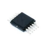
| 封装/外壳 | 10-TFSOP,10-MSOP(0.118",3.00mm 宽)裸焊盘 |
| 封装/箱体 | HVSSOP-10 |
| 工作温度 | -40°C ~ 125°C |
| 工厂包装数量 | 2500 |
| 开关频率 | 35 KHz to 1000 KHz |
| 最大工作温度 | + 125 C |
| 最小工作温度 | - 40 C |
| 标准包装 | 1 |
| 电压-电源 | 4.5 V ~ 52 V |
| 类型 | Current Mode PWM Controllers |
| 系列 | TPS40210 |
| 设计资源 | http://www.digikey.com/product-highlights/cn/zh/texas-instruments-webench-design-center/3176 |
| 输出数 | 1 |
| 输出电压 | 24 V |
| 输出电流 | 1 A |
| 输出端数量 | 1 Output |
| 配用 | /product-detail/zh/TPS40210EVM/296-30447-ND/1907866 |
| 降压 | 无 |
| 隔离式 | 无 |
| 频率-最大值 | 1MHz |


- 商务部:美国ITC正式对集成电路等产品启动337调查
- 曝三星4nm工艺存在良率问题 高通将骁龙8 Gen1或转产台积电
- 太阳诱电将投资9.5亿元在常州建新厂生产MLCC 预计2023年完工
- 英特尔发布欧洲新工厂建设计划 深化IDM 2.0 战略
- 台积电先进制程称霸业界 有大客户加持明年业绩稳了
- 达到5530亿美元!SIA预计今年全球半导体销售额将创下新高
- 英特尔拟将自动驾驶子公司Mobileye上市 估值或超500亿美元
- 三星加码芯片和SET,合并消费电子和移动部门,撤换高东真等 CEO
- 三星电子宣布重大人事变动 还合并消费电子和移动部门
- 海关总署:前11个月进口集成电路产品价值2.52万亿元 增长14.8%


PDF Datasheet 数据手册内容提取
Product Sample & Technical Tools & Support & Folder Buy Documents Software Community TPS40210,TPS40211 SLUS772F–MARCH2008–REVISEDMARCH2015 TPS4021x 4.5-V to 52-V Input Current Mode Boost Controller 1 Features 3 Description • ForBoost,Flyback,SEPIC,LEDDriveApps The TPS40210 and TPS40211 are wide-input voltage 1 (4.5 V to 52 V), nonsynchronous boost controllers. • WideInputOperatingVoltage:4.5Vto52V They are suitable for topologies which require a • AdjustableOscillatorFrequency grounded source N-channel FET including boost, • FixedFrequencyCurrentModeControl flyback, SEPIC and various LED Driver applications. The device features include programmable soft-start, • InternalSlopeCompensation overcurrent protection with automatic retry and • IntegratedLow-SideDriver programmable oscillator frequency. Current mode • ProgrammableClosed-LoopSoft-Start control provides improved transient response and simplified loop compensation. The main difference • OvercurrentProtection between the two parts is the reference voltage to • ExternalSynchronizationCapable whichtheerroramplifierregulatestheFBpin. • Reference700mV(TPS40210),260mV (TPS40211) DeviceInformation(1) • LowCurrentDisableFunction PARTNUMBER PACKAGE BODYSIZE(NOM) • CreateaCustomDesignUsingtheTPS4021x TPS40210 HVSSOP(10) 3.05mmx4.98mm withtheWEBENCHPowerDesigner TPS40211 VSON(10) 3.10mmx3.10mm (1) For all available packages, see the orderable addendum at 2 Applications theendofthedatasheet. • LEDLighting • IndustrialControlSystems • BatteryPoweredSystems SimplifiedSchematic V IN TPS40210 V 1 RC VDD 10 OUT 2 SS BP 9 3 DIS/EN GDRV 8 4 COMP ISNS 7 R 5 FB GND 6 SENSE UDG-07110 1 An IMPORTANT NOTICE at the end of this data sheet addresses availability, warranty, changes, use in safety-critical applications, intellectualpropertymattersandotherimportantdisclaimers.PRODUCTIONDATA.
TPS40210,TPS40211 SLUS772F–MARCH2008–REVISEDMARCH2015 www.ti.com Table of Contents 1 Features.................................................................. 1 7.4 DeviceFunctionalModes........................................23 2 Applications........................................................... 1 8 ApplicationandImplementation........................ 24 3 Description............................................................. 1 8.1 ApplicationInformation............................................24 4 RevisionHistory..................................................... 2 8.2 TypicalApplications................................................24 5 PinConfigurationandFunctions......................... 3 9 PowerSupplyRecommendations...................... 35 6 Specifications......................................................... 3 10 Layout................................................................... 35 6.1 AbsoluteMaximumRatings......................................3 10.1 LayoutGuidelines.................................................35 6.2 ESDRatings ............................................................4 10.2 LayoutExample....................................................35 6.3 RecommendedOperatingConditions.......................4 11 DeviceandDocumentationSupport................. 38 6.4 ThermalInformation..................................................4 11.1 DeviceSupport......................................................38 6.5 ElectricalCharacteristics...........................................4 11.2 DocumentationSupport .......................................38 6.6 TypicalCharacteristics..............................................6 11.3 RelatedLinks........................................................39 7 DetailedDescription............................................ 10 11.4 Trademarks...........................................................39 7.1 Overview.................................................................10 11.5 ElectrostaticDischargeCaution............................39 7.2 FunctionalBlockDiagram.......................................10 11.6 Glossary................................................................39 7.3 FeatureDescription.................................................11 12 Mechanical,Packaging,andOrderable Information........................................................... 39 4 Revision History NOTE:Pagenumbersforpreviousrevisionsmaydifferfrompagenumbersinthecurrentversion. ChangesfromRevisionE(October2011)toRevisionF Page • AddedUpdatedLandPattern................................................................................................................................................. 1 • AddedESDRatingstable,FeatureDescriptionsection,DeviceFunctionalModes,ApplicationandImplementation section,PowerSupplyRecommendationssection,Layoutsection,DeviceandDocumentationSupportsection,and Mechanical,Packaging,andOrderableInformationsection ................................................................................................. 1 ChangesfromRevisionD(April2010)toRevisionE Page • ChangedtheRevisiondatefromD,April2010toE,October2011...................................................................................... 1 • AddedQ1andQ3toFigure36byillustrator........................................................................................................................ 33 ChangesfromRevisionC(October2008)toRevisionD Page • ChangedC toC ......................................................................................................................................................... 19 ISNS IFLT • ChangedC toC ......................................................................................................................................................... 19 ISNS IFLT • Changedequations22and23............................................................................................................................................. 20 • Changedcorrectedequation25........................................................................................................................................... 21 • Added"R1isthehighsidefeedbackresistorinΩ"and"f isthedesiredloopcrossoverfrequency,inHz".....................21 L • Changedparagraphwithnewinput...................................................................................................................................... 21 • ChangedcapacitorvaluefromµFtoF................................................................................................................................. 21 • Changed0.2with0.1inMINcolinDesignExampleSpecificationstable........................................................................... 25 • DeletedtextfromPeakefficiencyrow.................................................................................................................................. 25 • Changed10Vwith8VinT conditionscolumn................................................................................................................ 25 OP • Changed42.8%to42.9%ineq32....................................................................................................................................... 26 • Added(V )andchangedapproximatedutycyclefrom42.8%to42.9%........................................................................... 26 FD • Changedequations32,34,35,36,37,38and39............................................................................................................... 26 • Changedequations47,48,49,50,51and53..................................................................................................................... 28 • Changedequations58,60,61,62....................................................................................................................................... 29 2 SubmitDocumentationFeedback Copyright©2008–2015,TexasInstrumentsIncorporated ProductFolderLinks:TPS40210 TPS40211
TPS40210,TPS40211 www.ti.com SLUS772F–MARCH2008–REVISEDMARCH2015 5 Pin Configuration and Functions DGQ DRC 10-Pin 10-Pin TopView TopView RC 1 10 VDD RC 1 110 VDD SS 2 9 BP SS 2 9 BP DIS/EN 3 8 GDRV DIS/EN 3 8 GDRV COMP 4 7 ISNS COMP 4 7 ISNS FB 5 6 GND FB 5 6 GND PinFunctions PIN I/O DESCRIPTION NAME NO. BP 9 O Regulatoroutputpin.Connecta1.0μFbypasscapacitorfromthispintoGND. COMP 4 O Erroramplifieroutput.ConnectcontrolloopcompensationnetworkbetweenCOMPpinandFBpin. Disablepin.Pullingthispinhigh,placesthepartintoashutdownmode.Shutdownmodeischaracterizedby averylowquiescentcurrent.Whileinshutdownmode,thefunctionalityofallblocksisdisabledandtheBP DIS/EN 3 I regulatorisshutdown.Thispinhasaninternal1MΩpull-downresistortoGND.Leavingthispin unconnectedenablesthedevice. Erroramplifierinvertinginput.Connectavoltagedividerfromtheoutputtothispintosetoutputvoltage. FB 5 I CompensationnetworkisconnectedbetweenthispinandCOMP. GDRV 8 O ConnectthegateofthepowerNchannelMOSFETtothispin. GND 6 - Deviceground. Currentsensepin.ConnectanexternalcurrentsensingresistorbetweenthispinandGND.Thevoltageon thispinisusedtoprovidecurrentfeedbackinthecontrolloopanddetectanovercurrentcondition.An ISNS 7 I overcurrentconditionisdeclaredwhenISNSpinvoltageexceedstheovercurrentthresholdvoltage,150mV typical. Switchingfrequencysettingpin.ConnectaresistorfromRCpintoVDDoftheICpowersupplyanda RC 1 I capacitorfromRCtoGND. Soft-starttimeprogrammingpin.ConnectcapacitorfromSSpintoGNDtoprogramconvertersoft-starttime. SS 2 I Thispinalsofunctionsasatimeouttimerwhenthepowersupplyisinanovercurrentcondition. Systeminputvoltage.ConnectalocalbypasscapacitorfromthispintoGND.Dependingontheamountof VDD 10 I requiredslopecompensation,thispincanbeconnectedtotheconverteroutput.SeeApplicationInformation sectionforadditionaldetails. 6 Specifications 6.1 Absolute Maximum Ratings overoperatingfree-airtemperaturerangeunlessotherwisenoted(1) MIN MAX UNIT VDD –0.3 52 Inputvoltage RC,SS,FB,DIS/EN –0.3 10 V ISNS –0.3 8 Outputvoltage COMP,BP,GDRV –0.3 9 T Operatingjunctiontemperature –40 150 °C J T Storagetemperature –55 150 °C stg (1) StressesbeyondthoselistedunderAbsoluteMaximumRatingsmaycausepermanentdamagetothedevice.Thesearestressratings only,andfunctionaloperationofthedeviceattheseoranyotherconditionsbeyondthoseindicatedunderRecommendedOperating Conditionsisnotimplied.Exposuretoabsolute-maximum-ratedconditionsforextendedperiodsmayaffectdevicereliability. Copyright©2008–2015,TexasInstrumentsIncorporated SubmitDocumentationFeedback 3 ProductFolderLinks:TPS40210 TPS40211
TPS40210,TPS40211 SLUS772F–MARCH2008–REVISEDMARCH2015 www.ti.com 6.2 ESD Ratings VALUE UNIT Human-bodymodel(HBM),perANSI/ESDA/JEDECJS-001(1) ±1500 V(ESD) Electrostaticdischarge Charged-devicemodel(CDM),perJEDECspecificationJESD22- ±1500 V C101(2) (1) JEDECdocumentJEP155statesthat500-VHBMallowssafemanufacturingwithastandardESDcontrolprocess. (2) JEDECdocumentJEP157statesthat250-VCDMallowssafemanufacturingwithastandardESDcontrolprocess. 6.3 Recommended Operating Conditions MIN MAX UNIT V Inputvoltage 4.5 52 V DD T OperatingJunctiontemperature -40 125 °C J 6.4 Thermal Information TPS40210 TPS40211 THERMALMETRIC(1) HVSSOP VSON UNIT 10PINS 10PINS R Junction-to-ambientthermalresistance 67.2 47.2 θJA R Junction-to-case(top)thermalresistance 50.5 74.6 θJC(top) R Junction-to-boardthermalresistance 41.0 22.2 θJB °C/W ψ Junction-to-topcharacterizationparameter 2.4 2.9 JT ψ Junction-to-boardcharacterizationparameter 40.7 22.4 JB R Junction-to-case(bottom)thermalresistance 15.6 8.8 θJC(bot) (1) Formoreinformationabouttraditionalandnewthermalmetrics,seetheICPackageThermalMetricsapplicationreport,SPRA953. 6.5 Electrical Characteristics T =–40°Cto125°C,V =12V ,allparametersatzeropowerdissipation(unlessotherwisenoted) J DD dc PARAMETER TESTCONDITIONS MIN TYP MAX UNIT VOLTAGEREFERENCE TPS40210 COMP=FB,4.5≤V ≤52V,T =25°C 693 700 707 DD J Feedbackvoltagerange TPS40211 COMP=FB,4.5≤V ≤52V,T =25°C 254 260 266 DD J VFB TPS40210 COMP=FB,4.5≤VDD≤52V,-40°C≤TJ≤ 686 700 714 mV 125°C COMP=FB,4.5≤V ≤52V,-40°C≤T ≤ TPS40211 DD J 250 260 270 125°C INPUTSUPPLY V Inputvoltagerange 4.5 52 V DD 4.5≤V ≤52V,noswitching,V <0.8 1.5 2.5 mA DD DIS I Operatingcurrent 2.5≤V ≤7V 10 20 μA DD DIS V <V ,V <0.8 530 μA DD UVLO(on) DIS UNDERVOLTAGELOCKOUT V Turnonthresholdvoltage 4.00 4.25 4.50 V UVLO(on) V UVLOhysteresis 140 195 240 mV UVLO(hyst) OSCILLATOR Oscillatorfrequencyrange(1) 35 1000 f kHz OSC Oscillatorfrequency R =182kΩ,C =330pF 260 300 340 RC RC Frequencylineregulation 4.5≤V ≤52V -20% 7% DD V Slopecompensationramp 520 620 720 mV SLP (1) Ensuredbydesign.Notproductiontested. 4 SubmitDocumentationFeedback Copyright©2008–2015,TexasInstrumentsIncorporated ProductFolderLinks:TPS40210 TPS40211
TPS40210,TPS40211 www.ti.com SLUS772F–MARCH2008–REVISEDMARCH2015 Electrical Characteristics (continued) T =–40°Cto125°C,V =12V ,allparametersatzeropowerdissipation(unlessotherwisenoted) J DD dc PARAMETER TESTCONDITIONS MIN TYP MAX UNIT PWM V =12V(1) 275 400 DD t Minimumpulsewidth ON(min) V =30V 90 200 ns DD t Minimumofftime 170 200 OFF(min) V Valleyvoltage 1.2 V VLY SOFT-START OffsetvoltagefromSSpintoerror V 700 mV SS(ofst) amplifierinput R Soft-startchargeresistance 320 430 600 SS(chg) kΩ R Soft-startdischargeresistance 840 1200 1600 SS(dchg) ERRORAMPLIFIER GBWP Unitygainbandwidthproduct(1) 1.5 3.0 MHz A Openloopgain(1) 60 80 dB OL Inputbiascurrent(currentoutofFB I 100 300 nA IB(FB) pin) I Outputsourcecurrent V =0.6V,V =1V 100 250 μA COMP(src) FB COMP I Outputsinkcurrent V =1.2V,V =1V 1.2 2.5 mA COMP(snk) FB COMP OVERCURRENTPROTECTION Overcurrentdetectionthreshold(at V 4.5≤V <52V,-40°C≤T ≤125°C 120 150 180 mV ISNS(oc) ISNSpin) DD J D Overcurrentdutycycle(1) 2% OC Overcurrentresetthresholdvoltage(at V 100 150 350 mV SS(rst) SSpin) T Leadingedgeblanking(1) 75 ns BLNK CURRENTSENSEAMPLIFIER A Currentsenseamplifiergain 4..2 5.6 7.2 V/V CS I Inputbiascurrent 1 3 μA B(ISNS) DRIVER I Gatedriversourcecurrent V =4V,T =25°C 375 400 GDRV(src) GDRV J mA I Gatedriversinkcurrent V =4V,T =25°C 330 400 GDRV(snk) GDRV J LINEARREGULATOR V Bypassvoltageoutput 0mA<I <15mA 7 8 9 V BP BP DISABLE/ENABLE V Turn-onvoltage 0.7 1.3 V DIS(en) V Hysteresisvoltage 25 130 220 mV DIS(hys) R DISpinpulldownresistance 0.7 1.1 1.5 MΩ DIS Copyright©2008–2015,TexasInstrumentsIncorporated SubmitDocumentationFeedback 5 ProductFolderLinks:TPS40210 TPS40211
TPS40210,TPS40211 SLUS772F–MARCH2008–REVISEDMARCH2015 www.ti.com 6.6 Typical Characteristics 1200 68pF CT(pF) 1200 33pF 470 1000 220 1000 100 68 kHz 800 33 kHz 800 ncy- 100pF ncy- ue 600 ue 600 q q Fre 220pF Fre f-SW400 f-SW400 200 200 470pF 0 0 0 0.2 0.4 0.6 0.8 1.0 1.2 100 200 300 400 500 600 700 800 900 1000 D-DutyCycle RT-TimingResistance-kW Figure1.FrequencyvsTimingResistance Figure2.SwitchingFrequencyvsDutyCycle 1.4 6 52V 1.2 4.5V 5 A A –m 1.0 –m Current 0.8 12V Current 4 uiescent 0.6 hutdown 3 Q S 2 I–VDD0.4 VVDD12V I–VDD 1 0.2 4.5V 52V 0 0 -40 -25 -10 5 20 35 50 65 80 95 110 125 -40 -25 -10 5 20 35 50 65 80 95 110 125 T –JunctionTemperature–°C T –JunctionTemperature–°C J J Figure3.QuiescentCurrentvsJunctionTemperature Figure4.ShutdownCurrentvsJunctionTemperature 0.4 0.5 52V 0.4 % 0.2 % – – 0.3 ge ge han 0.0 han 0.2 C C ge ge 0.1 olta -0.2 olta 0.0 V V nce nce-0.1 Refere -0.4 4.5V Refere-0.2 V–FB-0.6 12V VVDD142.5VV V–FB-0.3 52V -0.4 -0.8 -0.5 -40 -25 -10 5 20 35 50 65 80 95 110 125 0 10 20 30 40 50 60 TJ–JunctionTemperature–°C VVDD–InputVoltage – V Figure5.ReferenceVoltageChangevsJunction Figure6.ReferenceVoltageChangevsInputVoltage Temperature 6 SubmitDocumentationFeedback Copyright©2008–2015,TexasInstrumentsIncorporated ProductFolderLinks:TPS40210 TPS40211
TPS40210,TPS40211 www.ti.com SLUS772F–MARCH2008–REVISEDMARCH2015 Typical Characteristics (continued) 4.30 155 V UVLO VVDD 4.5V oltageLockoutThreshold–444...212550 OOfnf UVLOOn vercurrentThreshold–mV 111115555504213 4731..0255VVVV&20V 30V 7.5V Underv4.10 –OOC)149 12V&20V –VLO4.05 VISNS(148 VU UVLOOff 4.00 147 -40 -25 -10 5 20 35 50 65 80 95 110 125 -40 -25 -10 5 20 35 50 65 80 95 110 125 T –JunctionTemperature–°C T –JunctionTemperature–°C J J Figure7.UndervoltageLockoutThresholdvsJunction Figure8.OvercurrentThresholdvsJunctionTemperature Temperature 155 5 154 4 V % –m 153 e– 3 Threshold 115512 ncyChang 12 4.5V 12V nt ue Overcurre 114590 hingFreq -10 –OC)148 Switc -2 30V V (V) S(147 – -3 VDD N C 4.5V S S VI146 fO -4 1320VV 145 -5 0 5 10 15 20 25 30 35 40 45 -40 -25 -10 5 20 35 50 65 80 95 110 125 V –InputVoltage – V T –JunctionTemperature–°C VDD J Figure9.OvercurrentThresholdvsInputVoltage Figure10.SwitchingFrequencyChangevsJunction Temperature 29 1400 W V/V)VDDSLP 2275 4.5V Resistance-k11020000 RSS(DSCH) Discharge ( e o g Rati 23 24V 12V char 800 sation 21 ge/Dis 600 mpen Char SlopeCo 1179 36V VVDD123(V246)VVV SoftStart 420000 RSS(CHG)Charge 4.5V –S S 15 R 0 -40 -25 -10 5 20 35 50 65 80 95 110 125 -40 -25 -10 5 20 35 50 65 80 95 110 125 TJ–JunctionTemperature–°C TJ–JunctionTemperature–°C Figure11.OscillatorAmplitudevsJunctionTemperature Figure12.Soft-StartCharge/DischargeResistancevs JunctionTemperature Copyright©2008–2015,TexasInstrumentsIncorporated SubmitDocumentationFeedback 7 ProductFolderLinks:TPS40210 TPS40211
TPS40210,TPS40211 SLUS772F–MARCH2008–REVISEDMARCH2015 www.ti.com Typical Characteristics (continued) 180 300 A m 160 – –nA 140 urrent 250 nt C Curre 120 ource 200 –FeedbackBias 1086000 CompensationS 110500 IIB(FB) 40 –P(SRC) 50 20 M O C I 0 0 -40 -25 -10 5 20 35 50 65 80 95 110 125 -40 -25 -10 5 20 35 50 65 80 95 110 125 T –JunctionTemperature–°C T –JunctionTemperature–°C J J Figure13.FBBiasCurrentvsJunctionTemperature Figure14.CompensationSourceCurrentvsJunction Temperature 300 5 A m 4 ent– 250 % 3 SinkCurr 200 Change– 12 on ge Compensati 110500 ValleyVolta --210 – – P(SNK) 50 VVLY -3 OM -4 C I 0 -5 -40 -25 -10 5 20 35 50 65 80 95 110 125 -40 -25 -10 5 20 35 50 65 80 95 110 125 T –JunctionTemperature–°C T –JunctionTemperature–°C J J Figure15.CompensationSinkCurrentvsJunction Figure16.ValleyVoltageChangevsJunctionTemperature Temperature 8.8 1.10 V1.09 8.6 m V ILOAD=0mA old–1.08 Voltage– 88..42 OnThresh11..0067 ator urn-1.05 ul 8.0 T V–RegBP7.8 ILOAD=5mA –DIS/ENEN)111...000236 7.6 VDIS(1.01 7.4 1.00 -40 -25 -10 5 20 35 50 65 80 95 110 125 -40 -25 -10 5 20 35 50 65 80 95 110 125 T –JunctionTemperature–°C T –JunctionTemperature–°C J J Figure17.RegulatorVoltagevsJunctionTemperature Figure18.DIS/ENTurn-OnThresholdvsJunction Temperature 8 SubmitDocumentationFeedback Copyright©2008–2015,TexasInstrumentsIncorporated ProductFolderLinks:TPS40210 TPS40211
TPS40210,TPS40211 www.ti.com SLUS772F–MARCH2008–REVISEDMARCH2015 Typical Characteristics (continued) 7 V/V 6 – n ai G 5 er mplifi 4 A e s n 3 e S nt e urr 2 C – CS 1 A 0 -40 -25 -10 5 20 35 50 65 80 95 110 125 T –JunctionTemperature–°C J Figure19.CurrentSenseAmplifierGainvsJunctionTemperature Copyright©2008–2015,TexasInstrumentsIncorporated SubmitDocumentationFeedback 9 ProductFolderLinks:TPS40210 TPS40211
TPS40210,TPS40211 SLUS772F–MARCH2008–REVISEDMARCH2015 www.ti.com 7 Detailed Description 7.1 Overview The TPS4021x is a peak current-mode control low-side controller with a built in 400-mA gate driver designed to drive n- channel MOSFETs at a fixed frequency. The frequency is adjustable from 35 kHz to 1000 kHz. Small sizecombinedwithcompletefunctionalitymakesthepartbothversatileandeasytouse. Thecontrollerusesalow-valuecurrent-sensingresistorinserieswiththepowerMOSFET'ssourceconnectionto detect switching current. When the voltage drop across this resistor exceeds 150 mV, the part enters an hiccup faultmodewithatimeperiodsetbytheexternalsoft-startcapacitor. The TPS40210 uses voltage feedback to an error amplifier that is biased by a precision 700-mV reference. The TPS40211 has a lower 260-mV reference for higher efficiency in LED drive applications. Internal slope compensation eliminates the characteristic sub-harmonic instability of peak current mode control with duty cycles of50%orgreater. The TPS4021x also incorporates a soft-start feature where the output follows a slowly rising soft-start voltage, preventing output-voltage overshoot. The DIS/EN disables the TPS40210 putting it in a low quiescent current shutdownmode. 7.2 Functional Block Diagram DIS/EN 3 COMP 4 10 VDD FB 5 + + SS 2 LDO 9 BP E/A 700mV SoftStart SSRef and Overcurrent Driver OCFault PWM 8 GDRV EnableE/A Logic 6 GND Gain=6 + Oscillator and RC 1 Slope Compensation OCFault 7 ISNS 150mV UVLO + LEB UDG-07107 10 SubmitDocumentationFeedback Copyright©2008–2015,TexasInstrumentsIncorporated ProductFolderLinks:TPS40210 TPS40211
TPS40210,TPS40211 www.ti.com SLUS772F–MARCH2008–REVISEDMARCH2015 7.3 Feature Description 7.3.1 Soft-Start The soft-start feature of the TPS40210/11 is a closed-loop soft-start, meaning that the output voltage follows a linear ramp that is proportional to the ramp generated at the SS pin. This ramp is generated by an internal resistor connected from the BP pin to the SS pin and an external capacitor connected from the SS pin to GND. The SS pin voltage (V ) is level shifted down by approximately V (approximately 700 mV) and sent to one SS SS(ofst) of the “+” (the “+” input with the lowest voltage dominates) inputs of the error amplifier. When this level shifted voltage (V ) starts to rise at time t (see Figure 20), the output voltage the controller expects, rises as well. SSE 1 Since V starts at near 0 V, the controller attempts to regulate the output voltage from a starting point of zero SSE volts. It cannot do this due to the converter architecture. The output voltage starts from the input voltage less the drop across the diode (V - V ) and rises from there. The point at which the output voltage starts to rise (t ) is IN D 2 thepointwheretheV ramppassesthepointwhereitiscommandingmoreoutputvoltagethan(V -V ).This SSE IN D voltage level is labeled V . The time required for the output voltage to ramp from a theoretical zero to the SSE(1) final regulated value (from t to t ) is determined by the time it takes for the capacitor connected to the SS pin 1 3 (C )torisethrougha700-mVrange,beginningatV aboveGND. SS SS(ofst) TPS40210/11 V SS R SS(chg) 700mVREF SS ErrorAmplifier V +700mV SS(ofst) V 2 + V SSE + SS(ofst) R SS(dchg) V SSE(1) t t 0 1 V -V IN D V OUT t t 2 3 DIS UVLO OCFault FB 5 COMP 4 UDG-07121 Figure20.SSPinVoltageandOutputVoltage Figure21.SSPinFunctionalCircuit Copyright©2008–2015,TexasInstrumentsIncorporated SubmitDocumentationFeedback 11 ProductFolderLinks:TPS40210 TPS40211
TPS40210,TPS40211 SLUS772F–MARCH2008–REVISEDMARCH2015 www.ti.com Feature Description (continued) Therequiredcapacitanceforagivensoft-starttimet –t inFigure20iscalculatedinEquation1. 3 1 t C = SS SS æ ö V -V R ´lnç BP SS(ofst) ÷ SS çV -(V +V )÷ è BP SS(ofst) FB ø where • t isthesoft-starttime,inseconds SS • R istheSSchargingresistanceinΩ,typically500kΩ SS(chg) • C isthevalueofthecapacitorontheSSpin,inF SS • V isthevalueofthevoltageontheBPpin,inV BP • V istheapproximatelevelshiftfromtheSSpintotheerroramplifier(~700mV) SS(ofst) • V istheerroramplifierreferencevoltage,700mVtypical (1) FB Note that t is the time it takes for the output voltage to rise from 0 V to the final output voltage. Also note the SS tolerance on R given in the electrical specifications table. This contributes to some variability in the output SS(chg) voltagerisetimeandmarginmustbeappliedtoaccountforitindesign. Also take note of V . Its value varies depending on input conditions. For example, a converter operating from a BP slowly rising input initializes V at a fairly low value and increases during the entire startup sequence. If the BP controller has a voltage above 8V at the input and the DIS pin is used to stop and then restart the converter, V BP is approximately 8V for the entire startup sequence. The higher the voltage on BP, the shorter the startup time is andconversely,thelowerthevoltageonBP,thelongerthestartuptimeis. The soft-start time (t ) must be chosen long enough so that the converter can start up without going into an SS overcurrent state. Since the over current state is triggered by sensing the peak voltage on the ISNS pin, that voltage must be kept below the overcurrent threshold voltage V . The voltage on the ISNS pin is a function ISNS(oc) of the load current of the converter, the rate of rise of the output voltage and the output capacitance, and the current sensing resistor. The total output current that must be supported by the converter is the sum of the chargingcurrentrequiredbytheoutputcapacitorandanyexternalloadthatmustbesuppliedduringstartup.This current must be less than the I value used in Equation 15 or Equation 16 (depending on the operating OUT(oc) mode of the converter) to determine the current sense resistor value. In these equations, the actual input voltage at the time that the controller reaches the final output voltage is the important input voltage to use in the calculations. If the input voltage is slowly rising and is at less than the nominal input voltage when the startup time ends, the output current limit is less than I at the nominal input voltage. The output capacitor charging OUT(oc) current must be reduced (decrease C or increase the t ) or I must be increased and a new value for OUT SS OUT(oc) R calculated. ISNS C ´V I = OUT OUT C(chg) t SS (2) C ´V t > OUT OUT SS (I -I ) OUT(oc) EXT where • I istheoutputcapacitorchargingcurrentinA C(chg) • C isthetotaloutputcapacitanceinF OUT • V istheoutputvoltageinV OUT • t isthesoft-starttimefromEquation1 SS • I isthedesiredovercurrenttrippointinA OUT(oc) • I isanyexternalloadcurrentinA (3) EXT 12 SubmitDocumentationFeedback Copyright©2008–2015,TexasInstrumentsIncorporated ProductFolderLinks:TPS40210 TPS40211
TPS40210,TPS40211 www.ti.com SLUS772F–MARCH2008–REVISEDMARCH2015 Feature Description (continued) The capacitor on the SS pin (C ) also plays a role in overcurrent functionality. It is used as the timer between SS restartattempts.TheSSpinisconnectedtoGNDthrougharesistor,R ,wheneverthecontrollersensesan SS(dchg) overcurrent condition. Switching stops and nothing else happens until the SS pin discharges to the soft-start reset threshold, V . At this point, the SS pin capacitor is allowed to charge again through the charging SS(rst) resistor R , and the controller restarts from that point. The shortest time between restart attempts occurs SS(chg) when the SS pin discharges from V (approximately 700 mV) to V (150 mV) and then back to V SS(ofst) SS(rst) SS(ofst) and switching resumes. In actuality, this is a conservative estimate since switching does not resume until the V ramp rises to a point where it is commanding more output voltage than exists at the output of the controller. SSE This occurs at some SS pin voltage greater than V and depends on the voltage that remains on the output SS(ofst) overvoltage the converter while switching has been halted. The fastest restart time can be calculated by using Equation4,Equation5,andEquation6. æV ö t =R ´C ´lnç SS(ofst) ÷ DCHG SS(dchg) SS ç ÷ è VSS(rst) ø (4) ( ) æ V -V ö tCHG =RSS(chg)´CSS´lnçç(VBP-VSS(rst) )÷÷ è BP SS(ofst) ø (5) tRSTRT(min)=tCHG +tDCHG (6) V BP V SS t RSTR(min) V SS(ofst) V SS(rst) T-Time Figure22. Soft-StartduringOvercurrent 7.3.2 BPRegulator The TPS40210/11 has an on board linear regulator the supplies power for the internal circuitry of the controller, including the gate driver. This regulator has a nominal output voltage of 8 V and must be bypassed with a 1-μF capacitor. If the voltage at the VDD pin is less than 8 V, the voltage on the BP pin will also be less and the gate drive voltage to the external FET is reduced from the nominal 8 V. This should be considered when choosing a FETfortheconverter. Copyright©2008–2015,TexasInstrumentsIncorporated SubmitDocumentationFeedback 13 ProductFolderLinks:TPS40210 TPS40211
TPS40210,TPS40211 SLUS772F–MARCH2008–REVISEDMARCH2015 www.ti.com Feature Description (continued) Connecting external loads to this regulator can be done, but care must be taken to ensure that the thermal rating of the device is observed since there is no thermal shutdown feature in this controller. Exceeding the thermal ratings cause out of specification behavior and can lead to reduced reliability. The controller dissipates more power when there is an external load on the BP pin and is tested for dropout voltage for up to 5mA load. When the controller is in the disabled state, the BP pin regulator also shuts off so loads connected there power down aswell.WhenthecontrollerisdisabledwiththeDIS/ENpin,thisregulatoristurnedoff. The total power dissipation in the controller can be calculated as follows. The total power is the sum of P , P Q G andP . E P = V ´I Q VDD VDD(en) (7) P = V ´Q ´f G VDD g SW (8) P = V ´I E VDD EXT where • P isthequiescentpowerofthedeviceinW Q • V istheVDDpinvoltageinV DD • I isthequiescentcurrentofthecontrollerwhenenabledbutnotswitchinginA DD(en) • P isthepowerdissipatedbydrivingthegateoftheFETinW G • Q isthetotalgatechargeoftheFETatthevoltageontheBPpininC g • f istheswitchingfrequencyinHz SW • P isthedissipationcausedbeexternalloadingoftheBPpininW E • I istheexternalloadcurrentinA (9) EXT 7.3.3 Shutdown(DIS/ENPin) The DIS/EN pin is an active high shutdown command for the controller. Pulling this pin above 1.2 V causes the controller to completely shut down and enter a low current consumption state. In this state, the regulator connected to the BP pin is turned off. There is an internal 1.1-MΩ pulldown resistor connected to this pin that keeps the pin at GND level when left floating. If this function is not used in an application, it is best to connect thispintoGND. 7.3.4 MinimumOn-TimeandOff-TimeConsiderations The TPS40210 has a minimum off-time of approximately 200 ns and a minimum on-time of 300 ns. These two constraints place limitations on the operating frequency that can be used for a given input to output conversion ratio.SeeFigure2 forthemaximumfrequencythatcanbeusedforagivendutycycle. Thedutycycleatwhichtheconverteroperatesisdependentonthemodeinwhichtheconverterisrunning.Ifthe converter is running in discontinuous conduction mode, the duty cycle varies with changes to the load much morethanitdoeswhenrunningincontinuousconductionmode. Incontinuousconductionmode,thedutycycleisrelatedprimarilytotheinputandoutputvoltages. V +V 1 OUT D = V 1-D IN (10) æ æ V öö D=ç1-ç IN ÷÷ çè èVOUT +VD ø÷ø (11) In discontinuous mode the duty cycle is a function of the load, input and output voltages, inductance and switchingfrequency. ( ) 2´ V +V ´I ´L´f OUT D OUT SW D= ( )2 V IN (12) 14 SubmitDocumentationFeedback Copyright©2008–2015,TexasInstrumentsIncorporated ProductFolderLinks:TPS40210 TPS40211
TPS40210,TPS40211 www.ti.com SLUS772F–MARCH2008–REVISEDMARCH2015 Feature Description (continued) All converters using a diode as the freewheeling or catch component have a load current level at which they transition from discontinuous conduction to continuous conduction. This is the point where the inductor current just falls to zero. At higher load currents, the inductor current does not fall to zero but remains flowing in a positive direction and assumes a trapezoidal wave shape as opposed to a triangular wave shape. This load boundary between discontinuous conduction and continuous conduction can be found for a set of converter parametersasfollows. ( ) ( )2 V +V -V ´ V OUT D IN IN I = OUT(crit) ( )2 2´ V +V ´f ´L OUT D SW (13) For loads higher than the result of Equation 13, the duty cycle is given by Equation 11 and for loads less that the resultsofEquation13,thedutycycleisgivenEquation12.ForEquations1through4,thevariabledefinitionsare asfollows. • V istheoutputvoltageoftheconverterinV OUT • V istheforwardconductionvoltagedropacrosstherectifierorcatchdiodeinV D • V istheinputvoltagetotheconverterinV IN • I istheoutputcurrentoftheconverterinA OUT • ListheinductorvalueinH • f istheswitchingfrequencyinHz SW 7.3.5 SettingtheOscillatorFrequency TheoscillatorfrequencyisdeterminedbyaresistorandcapacitorconnectedtotheRCpinoftheTPS40210.The capacitor is charged to a level of approximately V /20 by current flowing through the resistor and is then DD discharged by a transistor internal to the TPS40210. The required resistor for a given oscillator frequency is foundfromeitherFigure1 orEquation14. 1 R = T 5.8´10-8 ´f ´C +8´10-10 ´f 2 +1.4´10-7 ´f -1.5´10-4 +1.7´10-6 ´C -4´10-9 ´C 2 SW T SW SW T T where • R isthetimingresistanceinkΩ T • f istheswitchingfrequencyinkHz SW • C isthetimingcapacitanceinpF (14) T For most applications a capacitor in the range of 68 pF to 120 pF gives the best results. Resistor values should be limited to between 100 kΩ and 1 MΩ as well. If the resistor value falls below 100 kΩ, decrease the capacitor size and recalculate the resistor value for the desired frequency. As the capacitor size decreases below 47 pF, the accuracy of Equation 14 degrades and empirical means may be needed to fine tune the timing component valuestoachievethedesiredswitchingfrequency. 7.3.6 SynchronizingtheOscillator The TPS40210 and TPS40211 can be synchronized to an external clock source. Figure 23 shows the functional diagramoftheoscillator.Whensynchronizingtheoscillatortoanexternalclock,theRCpinmustbepulledbelow 150 mV for 20 ns or more. The external clock frequency must be higher than the free running frequency of the converter as well. When synchronizing the controller, if the RC pin is held low for an excessive amount of time, erratic operation may occur. The maximum amount of time that the RC pin should be held low is 50% of a nominal output pulse, or 10% of the period of the synchronization frequency. If the external clock signal cannot operate with a low enough duty cycle to limit the amount of time the RC pin is held low, a resistor and capacitor can be added at the gate of the synchronization MOSFET. The capacitor should be added in series with the gate of the MOSFET to AC couple the rising edge of the synchronization signal. The resistor should be added from the gate of the MOSFET to ground to turn off the MOSFET. Typical values for the resistor and capacitor are 220 pFand1kΩ. Copyright©2008–2015,TexasInstrumentsIncorporated SubmitDocumentationFeedback 15 ProductFolderLinks:TPS40210 TPS40211
TPS40210,TPS40211 SLUS772F–MARCH2008–REVISEDMARCH2015 www.ti.com Feature Description (continued) Under circumstances where the duty cycle is less than 50%, a Schottky diode connected from the RC pin to an external clock may be used to synchronize the oscillator. The cathode of the diode is connected to the RC pin. The trip point of the oscillator is set by an internal voltage divider to be 1/20 of the input voltage. The clock signal must have an amplitude higher than this trip point. When the clock goes low, it allows the reset current to restart theRCramp,synchronizingtheoscillatortotheexternalclock.Thisprovidesasimple,single-componentmethod forclocksynchronization. VDD V 8 IN + CLK S Q R RC ExternalFrequency R Q Synchronization (optional) RC + 1 + 150mV C RC GND 5 TPS40210/11 UDG-08063 Figure23. OscillatorFunctionalDiagram VDD V 8 IN V Amplitude> IN + CLK 20 S Q R RC DutyCycle<50% R Q RC + 1 Frequency >Controller Frequency + 150mV C RC GND 5 TPS40210/11 UDG-08064 Figure24. DiodeConnectedSynchronization 16 SubmitDocumentationFeedback Copyright©2008–2015,TexasInstrumentsIncorporated ProductFolderLinks:TPS40210 TPS40211
TPS40210,TPS40211 www.ti.com SLUS772F–MARCH2008–REVISEDMARCH2015 Feature Description (continued) 7.3.7 CurrentSenseandOvercurrent The TPS4021x is a current mode controller that uses a resistor in series with the source terminal power FET to sensecurrentforboththecurrentmodecontrolandovercurrentprotection.Thedeviceentersacurrentlimitstate if the voltage on the ISNS pin exceeds the current limit threshold voltage V from the electrical ISNS(oc) specifications table. When this happens the controller discharges the SS capacitor through a relatively high impedance and then attempt to restart. The amount of output current that causes this to happen is dependent on severalvariablesintheconverter. TPS40210/11 V IN 10 VDD TPS40210/11 R T L V VDD 10 OUT 1 RC C T GDRV 8 6 GND R IFLT ISNS 7 UDG-07119 R C ISNS IFLT 6 GND UDG-07120 Figure25.OscillatorComponents Figure26.CurrentSenseComponents The load current overcurrent threshold is set by proper choice of R . If the converter is operating in ISNS discontinuousmodethecurrentsenseresistorisfoundinEquation15. f ´L´V SW ISNS(oc) R = ISNS ( ) 2´L´f ´I ´ V +V -V SW OUT(oc) OUT D IN (15) IftheconverterisoperatingincontinuousconductionmodeR canbefoundinEquation16. ISNS V V R = ISNS = ISNS ISNS æçèI1O-UDT ö÷ø+æçèIRIP2PLE ö÷ø æççè(I1O-UDT)ö÷÷ø+æçè2´Df´SWVIN´Lö÷ø where • R isthevalueofthecurrentsenseresistorinΩ. ISNS • V istheovercurrentthresholdvoltageattheISNSpin(fromelectricalspecifications) ISNS(oc) • Disthedutycycle(fromEquation11) • f istheswitchingfrequencyinHz SW • V istheinputvoltagetothepowerstageinV(seetext) IN • ListhevalueoftheinductorinH • I (oc)isthedesiredovercurrenttrippointinA OUT • V isthedropacrossthediodeinFigure26 (16) D Copyright©2008–2015,TexasInstrumentsIncorporated SubmitDocumentationFeedback 17 ProductFolderLinks:TPS40210 TPS40211
TPS40210,TPS40211 SLUS772F–MARCH2008–REVISEDMARCH2015 www.ti.com Feature Description (continued) The TPS40210/11 has a fixed undervoltage lockout (UVLO) that allows the controller to start at a typical input voltage of 4.25 V. If the input voltage is slowly rising, the converter might have less than its designed nominal input voltage available when it has reached regulation. As a result, this may decreases the apparent current limit load current value and must be taken into consideration when selecting R . The value of V used to calculate ISNS IN R must be the value at which the converter finishes startup. The total converter output current at startup is ISNS thesumoftheexternalloadcurrentandthecurrentrequiredtochargetheoutputcapacitor(s).SeetheSoft-Start sectionofthisdatasheetforinformationoncalculatingtherequiredoutputcapacitorchargingcurrent. The topology of the standard boost converter has no method to limit current from the input to the output in the event of a short circuit fault on the output of the converter. If protection from this type of event is desired, it is necessary to use some secondary protection scheme, such as a fuse, or rely on the current limit of the upstream powersource. 7.3.8 CurrentSenseandSub-HarmonicInstability A characteristic of peak current mode control results in a condition where the current control loop can exhibit instability. This results in alternating long and short pulses from the pulse width modulator. The voltage loop maintains regulation and does not oscillate, but the output ripple voltage increases. The condition occurs only when the converter is operating in continuous conduction mode and the duty cycle is 50% or greater. The cause of this condition is described in Texas Instruments literature number SLUA101, available at www.ti.com. The remedy for this condition is to apply a compensating ramp from the oscillator to the signal going to the pulse width modulator. In the TPS40210/11 the oscillator ramp is applied in a fixed amount to the pulse width modulator.TheslopeoftherampisgiveninEquation17. æV ö se =fSW ´çè V2D0D ÷ø (17) To ensure that the converter does not enter into sub-harmonic instability, the slope of the compensating ramp signalmustbeatleasthalfofthedownslopeofthecurrentrampsignal.Sincethecompensatingrampisfixedin theTPS40210/11,thisplacesaconstraintontheselectionofthecurrentsenseresistor. ThedownslopeofthecurrentsensewaveformatthepulsewidthmodulatorisdescribedinEquation18. ( ) A ´R ´ V +V -V CS ISNS OUT D IN m2= L (18) Since the slope compensation ramp must be at least half, and preferably equal to the down slope of the current sense waveform seen at the pulse width modulator, a maximum value is placed on the current sense resistor when operating in continuous mode at 50% duty cycle or greater. For design purposes, some margin should be applied to the actual value of the current sense resistor. As a starting point, the actual resistor chosen should be 80% or less that the value calculated in Equation 19. This equation calculates the resistor value that makes the slope compensation ramp equal to one half of the current ramp downslope. Values no more than 80% of this resultwouldbeacceptable. V ´L´f R = VDD SW ISNS(max) ( ) 60´ V +V -V OUT D IN where • S istheslopeofthevoltagecompensatingrampappliedtothepulsewidthmodulatorinV/s e • f istheswitchingfrequencyinHz SW • V isthevoltageattheVDDpininV DD • m2isthedownslopeofthecurrentsensewaveformseenatthepulsewidthmodulatorinV/s • R isthevalueofthecurrentsenseresistorinΩ ISNS • V istheconverteroutputvoltageV istheconverterpowerstageinputvoltage OUT IN • V isthedropacrossthediodeinFigure26 (19) D 18 SubmitDocumentationFeedback Copyright©2008–2015,TexasInstrumentsIncorporated ProductFolderLinks:TPS40210 TPS40211
TPS40210,TPS40211 www.ti.com SLUS772F–MARCH2008–REVISEDMARCH2015 Feature Description (continued) It is possible to increase the voltage compensation ramp slope by connecting the VDD pin to the output voltage of the converter instead of the input voltage as shown in Figure 26. This can help in situations where the converterdesigncallsforalargeripplecurrentvalueinrelationtothedesiredoutputcurrentlimitsetting. NOTE Connecting the VDD pin to the output voltage of the converter affects the startup voltage of the converter since the controller undervoltage lockout (UVLO) circuit monitors the VDD pin and senses the input voltage less the diode drop before startup. The effect is to increasethestartupvoltagebythevalueofthediodevoltagedrop. If an acceptable R value is not available, the next higher value can be used and the signal from the resistor ISNS divideddowntoanacceptablelevelbyplacinganotherresistorinparallelwithC . IFLT 7.3.9 CurrentSenseFiltering In most cases, a small filter placed on the ISNS pin improves performance of the converter. These are the components R and C in Figure 26. The time constant of this filter should be approximately 10% of the IFLT IFLT nominalpulsewidthoftheconverter.ThepulsewidthcanbefoundusingEquation20. D tON = f SW (20) Thesuggestedtimeconstantisthen R ´C =0.1´t IFLT IFLT ON (21) The range of R should be from about 1 kΩ to 5 kΩ for best results. Higher values can be used but this raises IFLT the impedance of the ISNS pin connection more than necessary and can lead to noise pickup issues in some layouts.C shouldbelocatedascloseaspossibletotheISNSpinaswelltoprovidenoiseimmunity. IFLT 7.3.10 ControlLoopConsiderations TherearetwomethodstodesignasuitablecontrolloopfortheTPS4021x.Thefirstandpreferredifequipmentis available is to use a frequency response analyzer to measure the open loop modulator and power stage gain and to then design compensation to fit that. The usage of these tools for this purpose is well documented with theliteraturethataccompaniesthetoolandisnotbediscussedhere. The second option is to make an initial guess at compensation, and then evaluate the transient response of the system to see if the compensation is acceptable to the application or not. For most systems, an adequate response can be obtained by simply placing a series resistor and capacitor (R and C ) from the COMP pin to FB FB the FB pin as shown in Figure 27. The initial compensation selection can be done more accurately with aid of WEBENCH® to select the compenents or the average Spice model to simulate the open loop modulator and powerstagegain. Copyright©2008–2015,TexasInstrumentsIncorporated SubmitDocumentationFeedback 19 ProductFolderLinks:TPS40210 TPS40211
TPS40210,TPS40211 SLUS772F–MARCH2008–REVISEDMARCH2015 www.ti.com Feature Description (continued) V IN TPS40210 L V 1 RC VDD 10 OUT 2 SS BP 9 C HF 3 DIS/EN GDRV 8 CFB RFB RIFLT COUT ROUT 4 COMP ISNS 7 CIFLT RSENSE 5 FB 6 GND R 1 R 2 UDG-07177 Figure27. BasicCompensationNetwork The natural phase characteristics of most capacitors used for boost outputs combined with the current mode control provide adequate phase margin when using this type of compensation. To determine an initial starting point for the compensation, the desired crossover frequency must be considered when estimating the control to outputgain.Themodelusedisacurrentsourceintotheoutputcapacitorandload. When using these equations, the loop bandwidth should be no more than 20% of the switching frequency, f . A SW more reasonable loop bandwidth would be 10% of the switching frequency. Be sure to evaluate the transient responseoftheconverterovertheexpectedloadrangetoensureacceptableoperation. K =g ´ Z (f ) CO M OUT CO (22) f 0.13´ L´ SW R OUT g = M (R )2´(120´R +L´f ) ISNS ISNS SW (23) ( ) ( )2 1+ 2p´f ´R ´C L ESR OUT Z =R ´ ( ) OUT OUT ( )2 ( )2 ( )2 1+ R +2´R ´R + R ´ 2p´f ´C OUT OUT ESR ESR L OUT where • K isthecontroltooutputgainoftheconverter,inV/V CO • g isthetransconductanceofthepowerstageandmodulator,inS M • R istheoutputloadequivalentresistance,inΩ OUT • Z istheoutputimpedance,includingtheoutputcapacitor,inΩ OUT • R isthevalueofthecurrentsenseresistor,inΩ ISNS • Listhevalueoftheinductor,inH 20 SubmitDocumentationFeedback Copyright©2008–2015,TexasInstrumentsIncorporated ProductFolderLinks:TPS40210 TPS40211
TPS40210,TPS40211 www.ti.com SLUS772F–MARCH2008–REVISEDMARCH2015 Feature Description (continued) • C isthevalueoftheoutputcapacitance,inF OUT • R istheequivalentseriesresistanceofC ,inΩ ESR OUT • f istheswitchingfrequency,inHz SW • f isthedesiredcrossoverfrequencyforthecontrolloop,inHz (24) L These equations assume that the operation is discontinuous and that the load is purely resistive. The gain in continuous conduction can be found by evaluating Equation 23 at the resistance that gives the critical conduction current for the converter. Loads that are more like current sources give slightly higher gains than predicted here. To find the gain of the compensation network required for a control loop of bandwidth f , take the reciprocal of L Equation22. 1 KCOMP = K CO (25) The GBWP of the error amplifier is only guaranteed to be at least 1.5MHz. If K multiplied by f is greater COMP L than 750 kHz, reduce the desired loop crossover frequency until this condition is satisfied. This ensures that the high-frequency pole from the error amplifier response with the compensation network in place does not cause excessivephaselagatf anddecreasedphasemarginintheloop. L The RC network connected from COMP to FB places a zero in the compensation response. That zero should be approximately 1/10th of the desired crossover frequency, f . With that being the case, R and C can be found L FB FB fromEquation26andEquation27 R1 R = =R1´K FB COMP K CO (26) 10 C = FB 2p´f ´R L FB where • R1isthehighsidefeedbackresistorinFigure27,inΩ • f isthedesiredloopcrossoverfrequency,inHz (27) L Thought not strictly necessary, it is recommended that a capacitor be added between COMP and FB to provide high-frequency noise attenuation in the control loop circuit. This capacitor introduces another pole in the compensation response. The allowable location of that pole frequency determines the capacitor value. As a startingpoint,thepolefrequencyshouldbe10× f .ThevalueofC canbefoundfromEquation28. L HF 1 C = HF 20p´f ´R L FB (28) While the error amplifier GBWP will usually be higher, it can be as low as 1.5MHz. If 10 × K × f > 1.5MHz, Comp L the error amplifier gain-bandwidth product may limit the high-frequency response below that of the high- frequencycapacitor.Tomaintainaconsistenthigh-frequencygainroll-off,C canbecalculatedbyEquation29. HF 1 C = HF ( )6 2p´1.5´ 10 ´R FB where • C isthehigh-frequencyroll-offcapacitorvalueinF HF • R isthemidbandgainsettingresistorvalueinΩ (29) FB Copyright©2008–2015,TexasInstrumentsIncorporated SubmitDocumentationFeedback 21 ProductFolderLinks:TPS40210 TPS40211
TPS40210,TPS40211 SLUS772F–MARCH2008–REVISEDMARCH2015 www.ti.com Feature Description (continued) 7.3.11 GateDriveCircuit Some applications benefit from the addition of a resistor connected between the GDRV pin and the gate of the switching MOSFET. In applications that have particularly stringent load regulation (under 0.75%) requirements and operate from input voltages above 5 V, or are sensitive to pulse jitter in the discontinuous conduction region, this resistor is recommended. The recommended starting point for the value of this resistor can be calculated fromEquation30. 105 RG = Q G where • Q istheMOSFETtotalgatechargeat8V,V innC G GS • R isthesuggestedstartingpointgateresistanceinΩ (30) G V IN TPS40210/11 L VDD 10 V OUT R G GDRV 8 ISNS 7 GND 6 UDG-07196 Figure28. GateDriveResistor 7.3.12 TPS40211 The only difference between the TPS40210 and the TPS40211 is the reference voltage that the error amplifier uses to regulate the output voltage. The TPS40211 uses a 260-mV reference and is intended for applications where the output is actually a current instead of a regulated voltage. A typical example of an application of this typeisanLEDdriver.AnexampleschematicisshowninFigure29. 22 SubmitDocumentationFeedback Copyright©2008–2015,TexasInstrumentsIncorporated ProductFolderLinks:TPS40210 TPS40211
TPS40210,TPS40211 www.ti.com SLUS772F–MARCH2008–REVISEDMARCH2015 Feature Description (continued) V IN I OUT TPS40210/11 L 1 RC VDD 10 2 SS BP 9 3 DIS/EN GDRV 8 4 COMP ISNS 7 R IFB 5 FB GND 6 UDG-07197 Figure29. TypicalLEDDriveSchematic ThecurrentintheLEDstringissetbythechoiceoftheresistorR asshowninEquation31. ISNS V RIFB = FB I OUT where • R isthevalueofthecurrentsenseresistorfortheLEDstringinΩ IFB • V isthereferencevoltagefortheTPS40211inV(0.260Vtyp.) FB • I isthedesiredDCcurrentintheLEDstringinA (31) OUT 7.4 Device Functional Modes 7.4.1 OperationNearMinimumInputVoltage The TPS4021x is designed to operate with input voltages above 4.5 V. The typical VDD UVLO threshold is 4.25 V and the device may operate at input voltages down to the UVLO voltage. At input voltages below the actual UVLO voltage, the device will not switch. When V passes the UVLO threshold the device will become active. VDD Switching is enabled and the soft-start sequence is initiated. The TPS4021x will ramp up the output voltage at theratedeterminedbytheexternalcapacitorattheSSpin. 7.4.2 OperationWithDIS/ENPin The DIS/EN pin has a 1.2-V typical threshold which can be used to disable the TPS4021x. With DIS/EN forced above this threshold voltage the device is disabled and switching is inhibited even if V is above its UVLO VDD threshold. Hysteresis on the DIS/EN pin threshold gives a typical turn-on threshold of 1.05 V. If the DIS/EN is left floating or is pulled below the 1.05-V threshold while V is above its UVLO threshold, the device becomes VDD active. Switching is enabled and the soft-start sequence is initiated. The TPS4021x will ramp up the output voltageattheratedeterminedbytheexternalcapacitoratthesoft-startpin. Copyright©2008–2015,TexasInstrumentsIncorporated SubmitDocumentationFeedback 23 ProductFolderLinks:TPS40210 TPS40211
TPS40210,TPS40211 SLUS772F–MARCH2008–REVISEDMARCH2015 www.ti.com 8 Application and Implementation NOTE Information in the following applications sections is not part of the TI component specification, and TI does not warrant its accuracy or completeness. TI’s customers are responsible for determining suitability of components for their purposes. Customers should validateandtesttheirdesignimplementationtoconfirmsystemfunctionality. 8.1 Application Information The TPS4021x is a 4.5-V to 52-V low-side controller with an integrated gate driver for a low-side N-channel MOSFET. This device is typically used in a boost topology to convert a lower DC voltage to a higher DC voltage with a peak current limit set by an external current sense resistor. It can also be configured in a SEPIC, Flyback and LED drive applications. In higher current applications, the maximum current can also be limited by the thermal performance of the external MOSFET and rectifying diode switch. Use the following design procedure to select external components for the TPS4021x. The design procedure illustrates the design of a typical boost regulator with the TPS40210. Alternatively, use the WEBENCH software to generate a complete design. The WEBENCH software uses an iterative design procedure and accesses a comprehensive database of componentswhengeneratingadesign. 8.2 Typical Applications 8.2.1 12-Vto24-VNonsynchronousBoostRegulator The following example illustrates the design process and component selection for a 12-V to 24-V nonsynchronousboostregulatorusingtheTPS40210controller. + + Figure30. TPS40210DesignExample –12-Vto24-Vat2A 24 SubmitDocumentationFeedback Copyright©2008–2015,TexasInstrumentsIncorporated ProductFolderLinks:TPS40210 TPS40211
TPS40210,TPS40211 www.ti.com SLUS772F–MARCH2008–REVISEDMARCH2015 Typical Applications (continued) 8.2.1.1 DesignRequirements Table1.TPS40210DesignExampleSpecifications PARAMETER TESTCONDITIONS MIN TYP MAX UNIT INPUTCHARACTERISTICS V Inputvoltage 8 12 14 V IN I Inputcurrent 4.4 IN A Noloadinputcurrent 0.05 V Inputundervoltagelockout 4.5 V IN(UVLO) OUTPUTCHARACTERISTICS V Outputvoltage 23.5 24.0 24.5 V OUT Lineregulation 1% Loadregulation 1% V Outputvoltageripple 500 mV OUT(ripple) PP I Outputcurrent 8V≤V ≤14V 0.1 1 2.0 OUT IN A I Outputovercurrentinceptionpoint 3.5 OCP Transientresponse ΔI Loadstep 1 A Loadslewrate 1 A/μs Overshootthresholdvoltage 500 mV Settlingtime 5 ms SYSTEMCHARACTERISTICS f Switchingfrequency 600 kHz SW η Peakefficiency V =12V 95% PK IN η Fullloadefficiency V =12V,I =2A 94% IN OUT T Operatingtemperaturerange 8V≤V ≤14V,I ≤2A 25 °C OP IN OUT MECHANICALDIMENSIONS W Width 1.5 L Length 1.5 inch h Height 0.5 8.2.1.2 DetailedDesignProcedure 8.2.1.2.1 CustomDesignwithWEBENCHTools ClickheretocreateacustomdesignusingtheTPS40210devicewiththe WEBENCH® PowerDesigner. 1. StartbyenteringyourV ,V andI requirements. IN OUT OUT 2. Optimize your design for key parameters like efficiency, footprint and cost using the optimizer dial and comparethisdesignwithotherpossiblesolutionsfromTexasInstruments. 3. WEBENCH Power Designer provides you with a customized schematic along with a list of materials with real timepricingandcomponentavailability. 4. Inmostcases,youwillalsobeableto: – Runelectricalsimulationstoseeimportantwaveformsandcircuitperformance, – Runthermalsimulationstounderstandthethermalperformanceofyourboard, – ExportyourcustomizedschematicandlayoutintopopularCADformats, – PrintPDFreportsforthedesign,andshareyourdesignwithcolleagues. 5. GetmoreinformationaboutWEBENCHtoolsatwww.ti.com/webench. 8.2.1.2.2 DutyCycleEstimation ThedutycycleofthemainswitchingMOSFETisestimatedusingEquation32andEquation33. Copyright©2008–2015,TexasInstrumentsIncorporated SubmitDocumentationFeedback 25 ProductFolderLinks:TPS40210 TPS40211
TPS40210,TPS40211 SLUS772F–MARCH2008–REVISEDMARCH2015 www.ti.com Typical Applications (continued) VOUT -VIN(max) +VFD 24V-14V+0.5V D » = =42.9% MIN V +V 24V+0.5V OUT FD (32) VOUT -VIN(min) +VFD 24V -8V +0.5V D » = = 67.3% MAX V +V 24V +0.5V OUT FD (33) Using an estimated forward drop (V ) of 0.5V for a schottky rectifier diode, the approximate duty cycle is 42.9% FD (minimum)to67.3%(maximum). 8.2.1.2.3 InductorSelection Thepeak-to-peakrippleischosentobe30%ofthemaximuminputcurrent. IOUT(max) 2 I =0.3´ =0.3´ =1.05A RIPPLE(max) 1-D 1-0.429 MIN (34) 26 SubmitDocumentationFeedback Copyright©2008–2015,TexasInstrumentsIncorporated ProductFolderLinks:TPS40210 TPS40211
TPS40210,TPS40211 www.ti.com SLUS772F–MARCH2008–REVISEDMARCH2015 Typical Applications (continued) TheminimuminductorsizecanbeestimatedusingEquation35. VIN(max) 1 14V 1 L » ´D ´ = ´0.429´ =9.5mH MIN I MIN f 1.05A 600kHz RIPPLE(max) SW (35) The next higher standard inductor value of 10 μH is selected. The ripple current for nominal and minimum V is IN estimatedbyEquation36andEquation37. V 1 12V 1 I » IN ´D´ = ´0.50´ =1.02A RIPPLE(Vintyp) L f 10mH 600kHz SW (36) V 1 8V 1 I » IN ´D´ = ´0.673´ =0.90A RIPPLE(Vinmin) L f 10mH 600kHz SW (37) The worst case peak-to-peak ripple current occurs at 50% duty cycle (V = 12.25 V) and is estimated as 1.02A. IN WorstcaseRMScurrentthroughtheinductorisapproximatedbyEquation38. ILrms = (IL(avg))2+(112IRIPPLE)2 » æççèI1O-UDT(MmAaXx)ö÷÷ø2+(112IRIPPLE(VINmin))2 = æçè1-02.673ö÷ø2+((112)´0.90A)2 =6.13Arms (38) TheworstcaseRMSinductorcurrentis6.13Arms.ThepeakinductorcurrentisestimatedbyEquation39. I » IOUT(max) +(1 )I = 2 +(1 )0.90=6.57A Lpeak 1-D 2 RIPPLE(Vinmin) 1-0.673 2 MAX (39) A 10-μH inductor with a minimum RMS current rating of 6.13A and minimum saturation current rating of 6.57 A mustbeselected.ATDKRLF12560T-100M-7R57.5-A10-μHinductorisselected. ThisinductorpowerdissipationisestimatedbyEquation40. ( )2 P » I ´DCR L Lrms (40) TheTDKRLF12560T-100M-7R512.4-mΩ DCRdissipates466-mWofpower. 8.2.1.2.4 RectifierDiodeSelection Alowforwardvoltagedropschottkydiodeisusedasarectifierdiodetoreduceitspowerdissipationandimprove efficiency.Using80%deratingonV forringingontheswitchnode,therectifierdiodeminimumreversebreak- OUT downvoltageisgivenbyEquation41. V V ³ OUT =1.25´V =1.25´24V =30V (BR)R(min) OUT 0.8 (41) The diode must have reverse breakdown voltage greater than 30 V. The rectifier diode peak and average currentsareestimatedbyEquation42andEquation43. ID(avg) »IOUT(max) = 2A (42) I =I =6.57A D(peak) L(peak) (43) ThepowerdissipationinthediodeisestimatedbyEquation44. P » V ´I =0.5V´2A =1W D(max) FD D(avg) (44) For this design, the maximum power dissipation is estimated as 1 W. Reviewing 30-V and 40-V schottky diodes, the MBRS340T3, 40-V, 3-A diode in an SMC package is selected. This diode has a forward voltage drop of 0.48 V at 6 A, so the conduction power dissipation is approximately 960 mW, less than half its rated power dissipation. Copyright©2008–2015,TexasInstrumentsIncorporated SubmitDocumentationFeedback 27 ProductFolderLinks:TPS40210 TPS40211
TPS40210,TPS40211 SLUS772F–MARCH2008–REVISEDMARCH2015 www.ti.com Typical Applications (continued) 8.2.1.2.5 OutputCapacitorSelection Outputcapacitorsmustbeselectedtomeettherequiredoutputrippleandtransientspecifications. I ´D 1 æ2A´0.673ö 1 COUT =8VOOUUTT(ripple) ´fSW =8çè 500mV ÷ø´600kHz =36mF (45) V 7 OUT(ripple) 7 500mV ESR= ´ = ´ =96mW 8 I -I 8 6.57A-2A L(peak) OUT (46) A Panasonic EEEFC1V330P 35-V 33-μF, 120-mΩ bulk capacitor and a 6.8-μF ceramic capacitor are selected to provide the required capacitance and ESR at the switching frequency. The combined capacitance of 39.8 μF and ESRof60mΩ areusedincompensationcalculations. 8.2.1.2.6 InputCapacitorSelection Since a boost converter has continuous input current, the input capacitor senses only the inductor ripple current. TheinputcapacitorvaluecanbecalculatedbyEquation47andEquation48. I 1.02A C > RIPPLE = =7.1mF IN 4´V ´f 4´60mV´600kHz IN(ripple) SW (47) V IN(ripple) 60mV ESR< = =29mW 2´I 2´1.02A RIPPLE (48) Forthisdesigntomeetamaximuminputrippleof60mV(1/2%ofV nominal),aminimum7.1-μFinputcapacitor IN withESRlessthan29mΩ isneeded.A10-μF,X7Rceramiccapacitorisselected. 8.2.1.2.7 CurrentSenseandCurrentLimit The maximum allowable current sense resistor value is limited by both the current limit and sub-harmonic stability.ThesetwolimitationsaregivenbyEquation49andEquation50. VISNS(OC)MIN 120mV R < = =15.4mW ISNS ( ) 1.1´(6.57A+0.50A) 1.1´ I +I L(peak) Drive (49) VIN(MAX)´L´fSW 14V´10mH´600kHz R < = =134mW ISNS 60´(V +V -V ) 60´(24V+0.48V-14V) OUT FD IN (50) With 10% margin on the current limit trip point (the 1.1 factor) and assuming a maximum gate drive current of 500 mA, the current limit requires a resistor less than 15.4 mΩ and stability requires a sense resistor less than 134 mΩ. A 10-mΩ resistor is selected. Approximately 2 mΩ of routing resistance is added in compensation calculations. ThepowerdissipationinR iscalculatedbyEquation51. ISNS PR =(ILRMS)2×RISNS×D ISNS (51) Atmaximumdutycycle,thisis0.253W. 8.2.1.2.8 CurrentSenseFilter To remove switching noise from the current sense, an RC filter is placed between the current sense resistor and the ISNS pin. A resistor with a value between 1 kΩ and 5 kΩ is selected and a capacitor value is calculated by Equation52. 0.1´D 0.1´0.429 C = MIN = =71pF IFLT f ´R 600kHz´1kW SW IFLT (52) Fora1-kΩ filterresistor,71pFiscalculatedanda100-pFcapacitorisselected. 28 SubmitDocumentationFeedback Copyright©2008–2015,TexasInstrumentsIncorporated ProductFolderLinks:TPS40210 TPS40211
TPS40210,TPS40211 www.ti.com SLUS772F–MARCH2008–REVISEDMARCH2015 Typical Applications (continued) 8.2.1.2.9 SwitchingMOSFETSelection The TPS40210 drives a ground referenced N-channel FET. The R and gate charge are estimated based on DS(on) thedesiredefficiencytarget. æ1 ö æ1 ö æ 1 ö PDISS(total) »POUT´ç -1÷= VOUT´IOUT´ç -1÷=24V´2A´ç -1÷=2.526W èh ø èh ø è0.95 ø (53) For a target of 95% efficiency with a 24-V Input voltage at 2 A, maximum power dissipation is limited to 2.526 W. The main power dissipating devices are the MOSFET, inductor, diode, current sense resistor and the integrated circuit,theTPS40210. P <P -P -P -P -V ´I FET DISS(total) L D Risns IN(max) VDD(max) (54) This leaves 812 mW of power dissipation for the MOSFET. This can likely cause an SO-8 MOSFET to get too hot, so power dissipation is limited to 500 mW. Allowing half for conduction and half for switching losses, we can determineatargetR andQ fortheMOSFETbyEquation55andEquation56. DS(on) GS 3´P ´I 3´0.50W´0.50A Q < FET DRIVE = =13.0nC GS 2´V ´I ´f 2´24V´2A´600kHz OUT OUT SW (55) A target MOSFET gate-to-source charge of less than 13.0 nC is calculated to limit the switching losses to less than250mW. P 0.50W R < FET = =9.9mW DS(on) 2´(I )2´D 2´6.132´0.673 RMS (56) A target MOSFET R of 9.9 mΩ is calculated to limit the conduction losses to less than 250 mW. Reviewing DS(on) 30-V and 40-V MOSFETs, an Si4386DY 9-mΩ MOSFET is selected. A gate resistor was added per Equation 30. ThemaximumgatechargeatV =8VfortheSi4386DYis33.2nC,thisimpliesR =3.3Ω. GS G 8.2.1.2.10 FeedbackDividerResistors The primary feedback divider resistor (R ) from V to FB should be selected between 10 kΩ and 100 kΩ to FB OUT maintain a balance between power dissipation and noise sensitivity. For a 24-V output a high feedback resistanceisdesirabletolimitpowerdissipationsoR =51.1kΩisselected. FB V ´R 0.700V´51.1kW R = FB FB = =1.53kW BIAS V -V 24V-0.700V OUT FB (57) R =1.50kΩisselected. BIAS 8.2.1.2.11 ErrorAmplifierCompensation Compensation selection can be done with aid of WEBENCH to select compensation components or with the aid oftheaverageSpicemodeltosimulatetheopenloopmodulatorandpowerstagegain.Alternativelythefollowing proceduregivesagoodstartingpoint. While current mode control typically only requires Type II compensation, it is desirable to layout for Type III compensation to increase flexibility during design and development. Current mode control boost converters have higher gain with higher output impedance, so it is necessary to calculate the control loop gain at the maximum outputimpedance,estimatedbyEquation58. V 24V ROUT(max)= IOUOT(UmTin) = 0.1A =240W (58) Copyright©2008–2015,TexasInstrumentsIncorporated SubmitDocumentationFeedback 29 ProductFolderLinks:TPS40210 TPS40211
TPS40210,TPS40211 SLUS772F–MARCH2008–REVISEDMARCH2015 www.ti.com Typical Applications (continued) ThetransconductanceoftheTPS40210currentmodecontrolcanbeestimatedbyEquation59. f 600kHz 0.13´ L´ SW 0.13´ 10mH´ ROUT 240W A g = = =19.2 M (R )2´(120´R +L´f ) (12mW)2´(120´12mW+10mH´600kHz) V ISNS ISNS SW (59) ThemaximumoutputimpedanceZ ,canbeestimatedbyEquation60. OUT ( ) ( )2 1+ 2p´f´R ´C ESR OUT Z (f) =R ´ ( ) OUT OUT ( )2 ( )2 ( )2 1+ R +2´R ´R + R ´ 2p´f´C OUT OUT ESR ESR OUT (60) ( ) 1+(2p´30kHz´60mW´39.8mF)2 ZOUT(fL) =240W´ ( ) =0.146W 1+ (240W)2 +2´240W´60mW+(60mW)2 ´(2p´30kHz´39.8mF)2 (61) Atthedesiredcrossoverfrequency(f )of30kHz,Z becomes0.146Ω. L OUT Themodulatorgainatthedesiredcross-overcanbeestimatedbyEquation62. K =g ´ Z (f ) =19.2A ´0.146W=2.80 CO M OUT CO V (62) The feedback compensation network needs to be designed to provide an inverse gain at the cross-over frequencyforunityloopgain.Thissetsthecompensationmid-bandgainatavaluecalculatedinEquation63. 1 1 KCOMP = = =0.357 K 2.80 CO (63) Tosetthemid-bandgainoftheerroramplifiertoK useEquation64. COMP R7 51.1kW R4=R7´K = = =18.2kW COMP K 2.80 CO (64) R4=18.7kΩ selected. Placethezeroat1/10thofthedesiredcross-overfrequency. 10 10 C2= = =2837pF 2p´f ´R4 2p´30kHz´18.7kW L (65) C2=2200pFselected. Place a high-frequency pole at about 5 times the desired cross-over frequency and less than one-half the unity gainbandwidthoftheerroramplifier: 1 1 C4» = =56.74pF 10p´f ´R4 10p´30kHz´18.7kW L (66) 1 1 C4> = =11.35pF p´GBW´R4 p´1.5MHz´18.7kW (67) C4=47pFselected. 8.2.1.2.12 RCOscillator The RC oscillator calculation is given as shown in Equation 14 in the datasheet, substituting 100 for C and 600 T for f . For a 600-kHz switching frequency, a 100pF capacitor is selected and a 262-kΩ resistor is calculated SW (261-kΩ selected). 30 SubmitDocumentationFeedback Copyright©2008–2015,TexasInstrumentsIncorporated ProductFolderLinks:TPS40210 TPS40211
TPS40210,TPS40211 www.ti.com SLUS772F–MARCH2008–REVISEDMARCH2015 Typical Applications (continued) 8.2.1.2.13 Soft-StartCapacitor SinceVDD>8V,thesoft-startcapacitorisselectedbyusingEquation68 tocalculatethevalue. C =20´T ´10-6 SS SS (68) ForT =12ms,C =240nF.A220-nFcapacitorisselected. SS SS 8.2.1.2.14 RegulatorBypass Aregulatorbypass(BP)capacitorof1.0 μFisselectedperthedatasheetrecommendation. 8.2.1.2.15 BillofMaterials Table2.BillofMaterials REFERENCE PART MANUFAC- DESCRIPTION SIZE DESIGNATOR NUMBER TURER C1 100μF,aluminumcapacitor,SM,±20%,35V 0.406x0.457 EEEFC1V101P Panasonic C2 2200pF,ceramiccapacitor,25V,X7R,20% 0603 Std Std C3 100pF,ceramiccapacitor,16V,C0G,10% 0603 Std Std C4 47pF,ceramiccapacitor,16V,X7R,20% 0603 Std Std C5 0.22μF,ceramiccapacitor,16V,X7R,20% 0603 Std Std C7 1.0μF,ceramiccapacitor,16V,X5R,20% 0603 Std Std C8 10μF,ceramiccapacitor,25V,X7R,20% 0805 C3225X7R1E106M TDK C9 0.1μF,ceramiccapacitor,50V,X7R,20% 0603 Std Std C10 100pF,ceramiccapacitor,16V,X7R,20% 0603 Std Std D1 Schottkydiode,3A,40V SMC MBRS340T3 OnSemi L1 10μH,inductor,SMT,7.5A,12.4mΩ 0.325x0.318inch RLF12560T-100M-7R5 TDK Q1 MOSFET,N-channel,40V,14A,9mΩ SO-8 Si4840DY Vishay R3 10kΩ,chipresistor,1/16W,5% 0603 Std Std R4 18.7kΩ,chipresistor,1/16W,1% 0603 Std Std R5 1.5kΩ,chipresistor,1/16W,1% 0603 Std Std R6 261kΩ,chipresistor,1/16W,1% 0603 Std Std R7 51.1kΩ,chipresistor,1/16W,1% 0603 Std Std R9 3.3Ω,chipresistor,1/16W,5% 0603 Std Std R10 1.0kΩ,chipresistor,1/16W,5% 0603 Std Std R11 10mΩ,chipresistor,1/2W,2% 1812 Std Std U1 IC,4.5V-52VI/P,currentmodeboostcontroller DGQ10 TPS40210DGQ TI Copyright©2008–2015,TexasInstrumentsIncorporated SubmitDocumentationFeedback 31 ProductFolderLinks:TPS40210 TPS40211
TPS40210,TPS40211 SLUS772F–MARCH2008–REVISEDMARCH2015 www.ti.com 8.2.1.3 ApplicationCurves 80 180 V =8V IN V =24V 60 135 OUT GDRV Phase IOUT=2A (5V/div) 40 90 20 45 B ° d – Gain– 0 Gain 0 Phase -20 -45 FETVds -40 -90 (20V/div) -60 -135 -80 -180 100 1000 10k 100k 1M fSW–Frequency–Hz T–Time–400ns Figure31.GainandPhasevsFrequency Figure32.FETVDSandVGSVoltagesvsTime 100 6 98 VIN(V1)4 VIN=14V VIN(V1)4 VIN=8V 12 5 12 96 8 8 94 W % s– 4 –Efficiency–h 89896082 VVININ==81V2V P–PowerLosLOSS 23 VVININ==1412VV 84 1 82 80 0 0 0.5 1.0 1.5 2.0 2.5 0 0.5 1.0 1.5 2.0 2.5 I –LoadCurrent– A I –LoadCurrent– A LOAD LOAD Figure33.EfficiencyvsLoadCurrent Figure34.PowerLossvsLoadCurrent 24.820 V (V) 24.772 IN 14 12 24.724 8 V V =8V e– 24.676 IN g a olt 24.628 V put 24.580 –Out 24.532 VIN=14V OUT24.484 VIN=12V V 24.436 24.388 24.340 0 0.5 1.0 1.5 2.0 2.5 I –LoadCurrent– A LOAD Figure35.OutputVoltagevsLoadCurrent 32 SubmitDocumentationFeedback Copyright©2008–2015,TexasInstrumentsIncorporated ProductFolderLinks:TPS40210 TPS40211
TPS40210,TPS40211 www.ti.com SLUS772F–MARCH2008–REVISEDMARCH2015 8.2.2 12-VInput,700-mALEDDriver,Upto35-VLEDString This application uses the TPS40211 as a boost controller that drives a string of LED diodes. The feedback point for this circuit is a sense resistor in series with this string. The low 260 mV reference minimizes power wasted in this resistor, and maintains the LED current at a value given by 0.26/R6. As the input voltage is varied, the duty cycle changes to maintain the LED current at a constant value so that the light intensity does not change with largeinputvoltagevariations. L1 VIN D1 R2 Q1 B2100 GDRV C3 C4 C21 C1 C2 R1 R11 ISNS VIN R3 D2 U1 C8 TPS40211 1 RC VIN 10 C10 C9 C11 2 SS BP 9 Loop Response DIS/EN 3 DIS/EN GDRV 8 GDRV LEDC Injection C6 4 COMP ISNS 7 ISNS R4 C5 R23 R13 C13 R24 LEDC 5 FB GND 6 R6 D3 R15 C14 Q3 PWMDimming UDG-08015 Figure36. 12-VInput,700-mALEDDriver,Upto35-VLEDString 8.2.2.1 DesignRequirements Table3.TPS40211DesignExampleSpecifications PARAMETER MIN TYP MAX UNIT INPUTCHARACTERISTICS V Inputvoltage 8 12 20 V IN OUTPUTCHARACTERISTICS V Outputvoltage 35 V OUT I Outputcurrent 0.7 A OUT SYSTEMCHARACTERISTICS f Switchingfrequency 400 kHz SW Copyright©2008–2015,TexasInstrumentsIncorporated SubmitDocumentationFeedback 33 ProductFolderLinks:TPS40210 TPS40211
TPS40210,TPS40211 SLUS772F–MARCH2008–REVISEDMARCH2015 www.ti.com 8.2.2.2 DetailedDesignProcedure Table4.TPS40211LEDDriverBillofMaterials REFERENCE TYPE DESCRIPTION SIZE DESIGNATOR C1,C2 10μF,25V 1206 C3,C4 2.2μF,100V 1210 C5 1nF,NPO 0603 C6 100pF,NPO 0603 C8 100pF 0603 C9 Capacitor 0.1μF 0603 C10 0.1μF,25V 0805 C11 1μF,25V 1206 C13 220pF 0603 C14 10nF,X7R 0603 C21 330μF,25Velectrolytic D1 B2100,SHTKY,100V,2A SMB D2 Diode BZT52C43 SOD-123 D3 MMBD7000 SOT-23 L1 Inductor Wurth7447709100,10μH,6A 12mm×12mm×10mm Q1 Si7850DP,60V,31mΩ SO-8 MOSFET Q3 2N7002,60V,0.1A SOT-23 R1 15mΩ 2512 R2 3.01Ω 0805 R3 402kΩ 0603 R4 14.3kΩ 0603 R6 0.36Ω 2512 Resistor R11 1kΩ 0603 R13 30.1kΩ 0603 R15 49.9kΩ 0603 R24 10kΩ 0603 R23 10Ω 0603 U1 Integratedcircuit TPS40211 DRC-10 34 SubmitDocumentationFeedback Copyright©2008–2015,TexasInstrumentsIncorporated ProductFolderLinks:TPS40210 TPS40211
TPS40210,TPS40211 www.ti.com SLUS772F–MARCH2008–REVISEDMARCH2015 9 Power Supply Recommendations The TPS4021x is designed to operate from an input voltage supply range between 4.5 V and 52 V. This input supply should remain within the input voltage range of the TPS4021x. If the input supply is located more than a few inches from the buck power stage controlled by the TPS4021x, additional bulk capacitance may be required inadditiontoceramic-bypasscapacitors.Anelectrolyticcapacitorwithavalueof100uFisatypicalchoice. 10 Layout 10.1 Layout Guidelines • ForthemaximumeffectivenessfromC9,placeitneartheVDDpinofthecontroller.Excessivehighfrequency noiseonVDDduringswitchingdegradesoverallregulationastheloadincreases. • Keeptheoutputloop(Q1-D1-C12-R11)assmallaspossible.Alargerloopcandegradecurrentlimitaccuracy andincreaserediatedemissions. • ForbestcurrentlimitaccuracykeeptheISNSfiltercomponentsC10andR10neartheISNSandGNDpins. • Avoid connecting traces carrying large AC currents through a ground plane. Instead, use PCB traces on the toplayertoconducttheACcurrentandusethegroundplaneasanoiseshield. • Split the ground plane as necessary to keep noise away from the TPS4021x and noise sensitive areas such as components connected to the RC pin, FB pin, COMP pin and SS pin. Also keep these noise sensitive componentsclosetotheTPS4021xIC. • KeepC7neartheBPandGNDpinstoprovidegoodbypassfortheBPregulator. • The GDRV trace should be as close as possible to the power FET gate to minimize parisitic resistance and inductance in the trace. The parasitics should also be minimized in the return path from the source of the MOSFET,throughthesenseresistorandbacktotheGNDpin. • KeeptheSWnodeasphysicallysmallaspossibletominimizeparasiticcapacitanceandradiatedemissions. • For good output voltage regulation, Kelvin connections should be brought from the load to the top FB resistor R7. 10.2 Layout Example Figure37. ComponentPlacement Copyright©2008–2015,TexasInstrumentsIncorporated SubmitDocumentationFeedback 35 ProductFolderLinks:TPS40210 TPS40211
TPS40210,TPS40211 SLUS772F–MARCH2008–REVISEDMARCH2015 www.ti.com Layout Example (continued) Figure38. TopCopper Figure39. BottomCopperViewedFromTop 36 SubmitDocumentationFeedback Copyright©2008–2015,TexasInstrumentsIncorporated ProductFolderLinks:TPS40210 TPS40211
TPS40210,TPS40211 www.ti.com SLUS772F–MARCH2008–REVISEDMARCH2015 Layout Example (continued) Figure40. Internal1CopperViewedFromTop Figure41. Internal2CopperViewedFromTop Copyright©2008–2015,TexasInstrumentsIncorporated SubmitDocumentationFeedback 37 ProductFolderLinks:TPS40210 TPS40211
TPS40210,TPS40211 SLUS772F–MARCH2008–REVISEDMARCH2015 www.ti.com 11 Device and Documentation Support 11.1 Device Support 11.1.1 Third-PartyProductsDisclaimer TI'S PUBLICATION OF INFORMATION REGARDING THIRD-PARTY PRODUCTS OR SERVICES DOES NOT CONSTITUTE AN ENDORSEMENT REGARDING THE SUITABILITY OF SUCH PRODUCTS OR SERVICES OR A WARRANTY, REPRESENTATION OR ENDORSEMENT OF SUCH PRODUCTS OR SERVICES, EITHER ALONEORINCOMBINATIONWITHANYTIPRODUCTORSERVICE. 11.1.2 RelatedDevices ThefollowingdeviceshavecharacteristicssimilartotheTPS40210andmaybeofinterest. Table5.RelatedParts DEVICE DESCRIPTION TPS6100x Single-andDual-CellBoostConverterwithStart-upintoFullLoad TPS6101x HighEfficiency1-Celland2-CellBoostConverters TPS6300x HighEfficiencySingleInductorBuck-BoostConverterwith1.8ASwitches 11.2 Documentation Support 11.2.1 CustomDesignwithWEBENCHTools ClickheretocreateacustomdesignusingtheTPS40210devicewiththe WEBENCH® PowerDesigner. 1. StartbyenteringyourV ,V andI requirements. IN OUT OUT 2. Optimize your design for key parameters like efficiency, footprint and cost using the optimizer dial and comparethisdesignwithotherpossiblesolutionsfromTexasInstruments. 3. WEBENCH Power Designer provides you with a customized schematic along with a list of materials with real timepricingandcomponentavailability. 4. Inmostcases,youwillalsobeableto: – Runelectricalsimulationstoseeimportantwaveformsandcircuitperformance, – Runthermalsimulationstounderstandthethermalperformanceofyourboard, – ExportyourcustomizedschematicandlayoutintopopularCADformats, – PrintPDFreportsforthedesign,andshareyourdesignwithcolleagues. 5. GetmoreinformationaboutWEBENCHtoolsatwww.ti.com/webench. 11.2.2 ReceivingNotificationofDocumentationUpdates To receive notification of documentation updates, navigate to the device product folder on ti.com. In the upper right corner, click on Alert me to register and receive a weekly digest of any product information that has changed.Forchangedetails,reviewtherevisionhistoryincludedinanyreviseddocument. 11.2.3 References These references may be found on the web at www.power.ti.com under Technical Documents. Many design toolsandlinkstoadditionalreferences,mayalsobefoundatwww.power.ti.com 1. Design and Application Guide for High Speed MOSFET Gate Drive Circuits, SEM 1400, 2001 Seminar Series 2. DesigningStableControlLoops,SEM1400,2001SeminarSeries 3. AdditionalPowerPAD™informationmaybefoundinApplicationsBriefsSLMA002 andSLMA004 4. QFN/SONPCBAttachment,SLUA271,June2002 38 SubmitDocumentationFeedback Copyright©2008–2015,TexasInstrumentsIncorporated ProductFolderLinks:TPS40210 TPS40211
TPS40210,TPS40211 www.ti.com SLUS772F–MARCH2008–REVISEDMARCH2015 11.3 Related Links The table below lists quick access links. Categories include technical documents, support and community resources,toolsandsoftware,andquickaccesstosampleorbuy. Table6.RelatedLinks TECHNICAL TOOLS& SUPPORT& PARTS PRODUCTFOLDER SAMPLE&BUY DOCUMENTS SOFTWARE COMMUNITY TPS40210 Clickhere Clickhere Clickhere Clickhere Clickhere TPS40211 Clickhere Clickhere Clickhere Clickhere Clickhere 11.4 Trademarks PowerPADisatrademarkofTexasInstruments. WEBENCHisaregisteredtrademarkofTexasInstruments. Allothertrademarksarethepropertyoftheirrespectiveowners. 11.5 Electrostatic Discharge Caution This integrated circuit can be damaged by ESD. Texas Instruments recommends that all integrated circuits be handled with appropriateprecautions.Failuretoobserveproperhandlingandinstallationprocedurescancausedamage. ESDdamagecanrangefromsubtleperformancedegradationtocompletedevicefailure.Precisionintegratedcircuitsmaybemore susceptibletodamagebecauseverysmallparametricchangescouldcausethedevicenottomeetitspublishedspecifications. 11.6 Glossary SLYZ022—TIGlossary. Thisglossarylistsandexplainsterms,acronyms,anddefinitions. 12 Mechanical, Packaging, and Orderable Information The following pages include mechanical, packaging, and orderable information. This information is the most current data available for the designated devices. This data is subject to change without notice and revision of thisdocument.Forbrowser-basedversionsofthisdatasheet,refertotheleft-handnavigation. Copyright©2008–2015,TexasInstrumentsIncorporated SubmitDocumentationFeedback 39 ProductFolderLinks:TPS40210 TPS40211
PACKAGE OPTION ADDENDUM www.ti.com 6-Feb-2020 PACKAGING INFORMATION Orderable Device Status Package Type Package Pins Package Eco Plan Lead/Ball Finish MSL Peak Temp Op Temp (°C) Device Marking Samples (1) Drawing Qty (2) (6) (3) (4/5) TPS40210DGQ ACTIVE HVSSOP DGQ 10 80 Green (RoHS NIPDAU | NIPDAUAG Level-1-260C-UNLIM -40 to 125 40210 & no Sb/Br) TPS40210DGQG4 ACTIVE HVSSOP DGQ 10 80 Green (RoHS NIPDAUAG Level-1-260C-UNLIM -40 to 125 40210 & no Sb/Br) TPS40210DGQR ACTIVE HVSSOP DGQ 10 2500 Green (RoHS NIPDAU | NIPDAUAG Level-1-260C-UNLIM -40 to 125 40210 & no Sb/Br) TPS40210DGQRG4 ACTIVE HVSSOP DGQ 10 2500 Green (RoHS NIPDAUAG Level-1-260C-UNLIM -40 to 125 40210 & no Sb/Br) TPS40210DRCR ACTIVE VSON DRC 10 3000 Green (RoHS NIPDAU Level-2-260C-1 YEAR -40 to 125 4210 & no Sb/Br) TPS40210DRCT ACTIVE VSON DRC 10 250 Green (RoHS NIPDAU Level-2-260C-1 YEAR -40 to 125 4210 & no Sb/Br) TPS40211DGQ ACTIVE HVSSOP DGQ 10 80 Green (RoHS NIPDAU | NIPDAUAG Level-1-260C-UNLIM -40 to 125 40211 & no Sb/Br) TPS40211DGQR ACTIVE HVSSOP DGQ 10 2500 Green (RoHS NIPDAU | NIPDAUAG Level-1-260C-UNLIM -40 to 125 40211 & no Sb/Br) TPS40211DRCR ACTIVE VSON DRC 10 3000 Green (RoHS NIPDAU Level-2-260C-1 YEAR -40 to 125 4211 & no Sb/Br) TPS40211DRCRG4 ACTIVE VSON DRC 10 3000 Green (RoHS NIPDAU Level-2-260C-1 YEAR -40 to 125 4211 & no Sb/Br) TPS40211DRCT ACTIVE VSON DRC 10 250 Green (RoHS NIPDAU Level-2-260C-1 YEAR -40 to 125 4211 & no Sb/Br) (1) The marketing status values are defined as follows: ACTIVE: Product device recommended for new designs. LIFEBUY: TI has announced that the device will be discontinued, and a lifetime-buy period is in effect. NRND: Not recommended for new designs. Device is in production to support existing customers, but TI does not recommend using this part in a new design. PREVIEW: Device has been announced but is not in production. Samples may or may not be available. OBSOLETE: TI has discontinued the production of the device. (2) RoHS: TI defines "RoHS" to mean semiconductor products that are compliant with the current EU RoHS requirements for all 10 RoHS substances, including the requirement that RoHS substance do not exceed 0.1% by weight in homogeneous materials. Where designed to be soldered at high temperatures, "RoHS" products are suitable for use in specified lead-free processes. TI may reference these types of products as "Pb-Free". RoHS Exempt: TI defines "RoHS Exempt" to mean products that contain lead but are compliant with EU RoHS pursuant to a specific EU RoHS exemption. Green: TI defines "Green" to mean the content of Chlorine (Cl) and Bromine (Br) based flame retardants meet JS709B low halogen requirements of <=1000ppm threshold. Antimony trioxide based flame retardants must also meet the <=1000ppm threshold requirement. Addendum-Page 1
PACKAGE OPTION ADDENDUM www.ti.com 6-Feb-2020 (3) MSL, Peak Temp. - The Moisture Sensitivity Level rating according to the JEDEC industry standard classifications, and peak solder temperature. (4) There may be additional marking, which relates to the logo, the lot trace code information, or the environmental category on the device. (5) Multiple Device Markings will be inside parentheses. Only one Device Marking contained in parentheses and separated by a "~" will appear on a device. If a line is indented then it is a continuation of the previous line and the two combined represent the entire Device Marking for that device. (6) Lead/Ball Finish - Orderable Devices may have multiple material finish options. Finish options are separated by a vertical ruled line. Lead/Ball Finish values may wrap to two lines if the finish value exceeds the maximum column width. Important Information and Disclaimer:The information provided on this page represents TI's knowledge and belief as of the date that it is provided. TI bases its knowledge and belief on information provided by third parties, and makes no representation or warranty as to the accuracy of such information. Efforts are underway to better integrate information from third parties. TI has taken and continues to take reasonable steps to provide representative and accurate information but may not have conducted destructive testing or chemical analysis on incoming materials and chemicals. TI and TI suppliers consider certain information to be proprietary, and thus CAS numbers and other limited information may not be available for release. In no event shall TI's liability arising out of such information exceed the total purchase price of the TI part(s) at issue in this document sold by TI to Customer on an annual basis. OTHER QUALIFIED VERSIONS OF TPS40210, TPS40211 : •Automotive: TPS40210-Q1, TPS40211-Q1 •Enhanced Product: TPS40210-EP NOTE: Qualified Version Definitions: •Automotive - Q100 devices qualified for high-reliability automotive applications targeting zero defects •Enhanced Product - Supports Defense, Aerospace and Medical Applications Addendum-Page 2
PACKAGE MATERIALS INFORMATION www.ti.com 6-Sep-2019 TAPE AND REEL INFORMATION *Alldimensionsarenominal Device Package Package Pins SPQ Reel Reel A0 B0 K0 P1 W Pin1 Type Drawing Diameter Width (mm) (mm) (mm) (mm) (mm) Quadrant (mm) W1(mm) TPS40210DGQR HVSSOP DGQ 10 2500 330.0 12.4 5.3 3.4 1.4 8.0 12.0 Q1 TPS40210DGQR HVSSOP DGQ 10 2500 330.0 12.4 5.3 3.3 1.3 8.0 12.0 Q1 TPS40210DRCR VSON DRC 10 3000 330.0 12.4 3.3 3.3 1.1 8.0 12.0 Q2 TPS40210DRCT VSON DRC 10 250 180.0 12.4 3.3 3.3 1.1 8.0 12.0 Q2 TPS40211DGQR HVSSOP DGQ 10 2500 330.0 12.4 5.3 3.4 1.4 8.0 12.0 Q1 TPS40211DRCR VSON DRC 10 3000 330.0 12.4 3.3 3.3 1.1 8.0 12.0 Q2 TPS40211DRCT VSON DRC 10 250 180.0 12.4 3.3 3.3 1.1 8.0 12.0 Q2 PackMaterials-Page1
PACKAGE MATERIALS INFORMATION www.ti.com 6-Sep-2019 *Alldimensionsarenominal Device PackageType PackageDrawing Pins SPQ Length(mm) Width(mm) Height(mm) TPS40210DGQR HVSSOP DGQ 10 2500 364.0 364.0 27.0 TPS40210DGQR HVSSOP DGQ 10 2500 346.0 346.0 35.0 TPS40210DRCR VSON DRC 10 3000 367.0 367.0 35.0 TPS40210DRCT VSON DRC 10 250 210.0 185.0 35.0 TPS40211DGQR HVSSOP DGQ 10 2500 364.0 364.0 27.0 TPS40211DRCR VSON DRC 10 3000 367.0 367.0 35.0 TPS40211DRCT VSON DRC 10 250 210.0 185.0 35.0 PackMaterials-Page2
None
None
None
None
None
GENERIC PACKAGE VIEW DRC 10 VSON - 1 mm max height PLASTIC SMALL OUTLINE - NO LEAD Images above are just a representation of the package family, actual package may vary. Refer to the product data sheet for package details. 4204102-3/M
PACKAGE OUTLINE DRC0010J VSON - 1 mm max height SCALE 4.000 PLASTIC SMALL OUTLINE - NO LEAD 3.1 B A 2.9 PIN 1 INDEX AREA 3.1 2.9 1.0 C 0.8 SEATING PLANE 0.05 0.00 0.08 C 1.65 0.1 2X (0.5) (0.2) TYP EXPOSED 4X (0.25) THERMAL PAD 5 6 2X 11 SYMM 2 2.4 0.1 10 1 8X 0.5 0.30 10X 0.18 PIN 1 ID SYMM 0.1 C A B (OPTIONAL) 0.5 0.05 C 10X 0.3 4218878/B 07/2018 NOTES: 1. All linear dimensions are in millimeters. Any dimensions in parenthesis are for reference only. Dimensioning and tolerancing per ASME Y14.5M. 2. This drawing is subject to change without notice. 3. The package thermal pad must be soldered to the printed circuit board for optimal thermal and mechanical performance. www.ti.com
EXAMPLE BOARD LAYOUT DRC0010J VSON - 1 mm max height PLASTIC SMALL OUTLINE - NO LEAD (1.65) (0.5) 10X (0.6) 1 10 10X (0.24) 11 SYMM (2.4) (3.4) (0.95) 8X (0.5) 6 5 (R0.05) TYP ( 0.2) VIA TYP (0.25) (0.575) SYMM (2.8) LAND PATTERN EXAMPLE EXPOSED METAL SHOWN SCALE:20X 0.07 MIN 0.07 MAX EXPOSED METAL ALL AROUND ALL AROUND EXPOSED METAL SOLDER MASK METAL METAL UNDER SOLDER MASK OPENING SOLDER MASK OPENING NON SOLDER MASK SOLDER MASK DEFINED DEFINED (PREFERRED) SOLDER MASK DETAILS 4218878/B 07/2018 NOTES: (continued) 4. This package is designed to be soldered to a thermal pad on the board. For more information, see Texas Instruments literature number SLUA271 (www.ti.com/lit/slua271). 5. Vias are optional depending on application, refer to device data sheet. If any vias are implemented, refer to their locations shown on this view. It is recommended that vias under paste be filled, plugged or tented. www.ti.com
EXAMPLE STENCIL DESIGN DRC0010J VSON - 1 mm max height PLASTIC SMALL OUTLINE - NO LEAD 2X (1.5) (0.5) SYMM EXPOSED METAL 11 TYP 10X (0.6) 1 10 (1.53) 10X (0.24) 2X (1.06) SYMM (0.63) 8X (0.5) 6 5 (R0.05) TYP 4X (0.34) 4X (0.25) (2.8) SOLDER PASTE EXAMPLE BASED ON 0.125 mm THICK STENCIL EXPOSED PAD 11: 80% PRINTED SOLDER COVERAGE BY AREA SCALE:25X 4218878/B 07/2018 NOTES: (continued) 6. Laser cutting apertures with trapezoidal walls and rounded corners may offer better paste release. IPC-7525 may have alternate design recommendations. www.ti.com
IMPORTANTNOTICEANDDISCLAIMER TI PROVIDES TECHNICAL AND RELIABILITY DATA (INCLUDING DATASHEETS), DESIGN RESOURCES (INCLUDING REFERENCE DESIGNS), APPLICATION OR OTHER DESIGN ADVICE, WEB TOOLS, SAFETY INFORMATION, AND OTHER RESOURCES “AS IS” AND WITH ALL FAULTS, AND DISCLAIMS ALL WARRANTIES, EXPRESS AND IMPLIED, INCLUDING WITHOUT LIMITATION ANY IMPLIED WARRANTIES OF MERCHANTABILITY, FITNESS FOR A PARTICULAR PURPOSE OR NON-INFRINGEMENT OF THIRD PARTY INTELLECTUAL PROPERTY RIGHTS. These resources are intended for skilled developers designing with TI products. You are solely responsible for (1) selecting the appropriate TI products for your application, (2) designing, validating and testing your application, and (3) ensuring your application meets applicable standards, and any other safety, security, or other requirements. These resources are subject to change without notice. TI grants you permission to use these resources only for development of an application that uses the TI products described in the resource. Other reproduction and display of these resources is prohibited. No license is granted to any other TI intellectual property right or to any third party intellectual property right. TI disclaims responsibility for, and you will fully indemnify TI and its representatives against, any claims, damages, costs, losses, and liabilities arising out of your use of these resources. TI’s products are provided subject to TI’s Terms of Sale (www.ti.com/legal/termsofsale.html) or other applicable terms available either on ti.com or provided in conjunction with such TI products. TI’s provision of these resources does not expand or otherwise alter TI’s applicable warranties or warranty disclaimers for TI products. Mailing Address: Texas Instruments, Post Office Box 655303, Dallas, Texas 75265 Copyright © 2020, Texas Instruments Incorporated