ICGOO在线商城 > 集成电路(IC) > PMIC - 监控器 > TPS3705-33DR
 Datasheet下载
- 型号: TPS3705-33DR
- 制造商: Texas Instruments
- 库位|库存: xxxx|xxxx
- 要求:
| 数量阶梯 | 香港交货 | 国内含税 |
| +xxxx | $xxxx | ¥xxxx |
查看当月历史价格
查看今年历史价格
TPS3705-33DR产品简介:
ICGOO电子元器件商城为您提供TPS3705-33DR由Texas Instruments设计生产,在icgoo商城现货销售,并且可以通过原厂、代理商等渠道进行代购。 TPS3705-33DR价格参考¥11.52-¥20.62。Texas InstrumentsTPS3705-33DR封装/规格:PMIC - 监控器, Supervisor Push-Pull, Totem Pole 1 Channel 8-SOIC。您可以下载TPS3705-33DR参考资料、Datasheet数据手册功能说明书,资料中有TPS3705-33DR 详细功能的应用电路图电压和使用方法及教程。
TPS3705-33DR是Texas Instruments(德州仪器)生产的一款高精度电压监控器,属于PMIC - 监控器类别。该器件主要用于监测系统电源电压是否稳定,确保系统在安全电压范围内运行。其典型应用包括电池供电设备、嵌入式系统、工业控制、通信设备和消费类电子产品。

该芯片具有3.3V的固定阈值检测功能,当供电电压低于设定阈值时,会触发复位信号,防止微处理器或微控制器在电压不足的情况下误操作或崩溃,从而提高系统的可靠性。其响应速度快,能够及时响应电压跌落,适用于对电源稳定性要求较高的场景。

由于采用小型化SOT-23封装,TPS3705-33DR适合空间受限的应用,如便携式医疗设备、智能传感器和物联网终端等。同时,其低功耗特性使其非常适合电池长期供电的系统,有助于延长设备工作时间。

此外,该器件具备高抗噪声能力,可在电磁干扰较强的工业环境中稳定工作,广泛应用于PLC模块、电机驱动器和自动化控制系统中作为上电复位或掉电保护电路的关键元件。

综上所述,TPS3705-33DR是一款高可靠性、低功耗、小尺寸的电压监控器,适用于需要精准电源管理与系统保护的多种电子设备。
| 参数 | 数值 |
| 产品目录 | 集成电路 (IC) |
| 描述 | IC 2.93V PROCESSOR MON 8-SOIC |
| 产品分类 | |
| 品牌 | Texas Instruments |
| 数据手册 | |
| 产品图片 |
|
| 产品型号 | TPS3705-33DR |
| rohs | 无铅 / 符合限制有害物质指令(RoHS)规范要求 |
| 产品系列 | - |
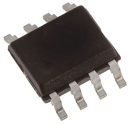
| 供应商器件封装 | 8-SOIC |
| 其它名称 | 296-26940-1 |
| 包装 | 剪切带 (CT) |
| 受监控电压数 | 1 |
| 复位 | 低有效 |
| 复位超时 | 最小为 140 ms |
| 安装类型 | 表面贴装 |
| 封装/外壳 | 8-SOIC(0.154",3.90mm 宽) |
| 工作温度 | -40°C ~ 85°C |
| 标准包装 | 1 |
| 电压-阈值 | 2.93V |
| 类型 | 简单复位/加电复位 |
| 输出 | 推挽式,图腾柱 |


- 商务部:美国ITC正式对集成电路等产品启动337调查
- 曝三星4nm工艺存在良率问题 高通将骁龙8 Gen1或转产台积电
- 太阳诱电将投资9.5亿元在常州建新厂生产MLCC 预计2023年完工
- 英特尔发布欧洲新工厂建设计划 深化IDM 2.0 战略
- 台积电先进制程称霸业界 有大客户加持明年业绩稳了
- 达到5530亿美元!SIA预计今年全球半导体销售额将创下新高
- 英特尔拟将自动驾驶子公司Mobileye上市 估值或超500亿美元
- 三星加码芯片和SET,合并消费电子和移动部门,撤换高东真等 CEO
- 三星电子宣布重大人事变动 还合并消费电子和移动部门
- 海关总署:前11个月进口集成电路产品价值2.52万亿元 增长14.8%


PDF Datasheet 数据手册内容提取
Product Order Technical Tools & Support & Folder Now Documents Software Community TPS3705-30,TPS3705-33,TPS3705-50,TPS3707-30,TPS3707-50 SLVS184E–NOVEMBER1998–REVISEDJULY2017 TPS370x-xx Processor Supervisory Circuits With Power-Fail 1 Features 3 Description • Power-OnResetGeneratorWithFixedDelay The TPS370x-xx family of microprocessor supply- 1 voltage supervisors provide circuit initialization and Timeof200ms(NoExternalCapacitorNeeded) timing supervision, primarily for DSP and processor- • PrecisionSupplyVoltageMonitor:2.5V,3V, basedsystems. 3.3V,and5V During power-on, RESET is asserted when the • Pin-for-PinCompatibleWiththeMAX705Through supply voltage V becomes higher than 1.1 V. MAX708Series DD Thereafter, the supply voltage supervisor monitors • IntegratedWatchdogTime(TPS3705-xxOnly) V and keeps RESET active as long as V remains DD DD • VoltageMonitorforPower-FailorLow-Battery below the threshold voltage VIT+. When the supply Warning voltage drops below the threshold voltage VIT–, the output becomes active (low) again. No external • MaximumSupplyCurrentof50 µA components are required. All the devices of this • 8-PinMSOPand8-PinSOICPackages family have a fixed-sense threshold voltage V set IT– • TemperatureRange:–40°Cto85°C byaninternalvoltagedivider. The product spectrum is designed for supply voltages 2 Applications of 2.5 V, 3 V, 3.3 V, and 5 V. The circuits are • DesignsUsingDSPs,Microcontrollers,or available in either 8-pin MSOP or standard SOIC packages. The TPS370x-xx devices are Microprocessors characterized for operation over a temperature range • IndustrialEquipment of−40°Cto85°C. • ProgrammableControls • AutomotiveSystems DeviceInformation(1) • PortableorBatteryPoweredEquipment PARTNUMBER PACKAGE BODYSIZE(NOM) • IntelligentInstruments TPS3705-xx, MPoSwOePrP-AD™(8) 3.00mm×3.00mm • WirelessCommunicationSystems TPS3707-xx SOIC(8) 3.90mm×4.90mm • NotebookorDesktopComputers (1) For all available packages, see the orderable addendum at theendofthedatasheet. TypicalMSP430Application 12 V 5 V VDD VDD PFO TPS3705−50 MSP430P112 100nF MR RESET RESET/NMI 910 kΩ WDO I/O PFI WDI I/O 120 kΩ GND GND Copyright © 2016,Texas Instruments Incorporated 1 An IMPORTANT NOTICE at the end of this data sheet addresses availability, warranty, changes, use in safety-critical applications, intellectualpropertymattersandotherimportantdisclaimers.PRODUCTIONDATA.
TPS3705-30,TPS3705-33,TPS3705-50,TPS3707-30,TPS3707-50 SLVS184E–NOVEMBER1998–REVISEDJULY2017 www.ti.com Table of Contents 1 Features.................................................................. 1 8.1 Overview.................................................................11 2 Applications........................................................... 1 8.2 FunctionalBlockDiagram.......................................11 3 Description............................................................. 1 8.3 FeatureDescription................................................11 8.4 DeviceFunctionalModes........................................12 4 RevisionHistory..................................................... 2 9 ApplicationandImplementation........................ 13 5 DeviceComparisonTable..................................... 3 9.1 ApplicationInformation............................................13 6 PinConfigurationandFunctions......................... 4 9.2 TypicalApplication .................................................13 7 Specifications......................................................... 5 10 PowerSupplyRecommendations..................... 14 7.1 AbsoluteMaximumRatings......................................5 11 Layout................................................................... 14 7.2 ESDRatings ............................................................5 11.1 LayoutGuidelines.................................................14 7.3 RecommendedOperatingConditions.......................5 11.2 LayoutExample....................................................14 7.4 ThermalInformation..................................................6 12 DeviceandDocumentationSupport................. 15 7.5 ElectricalCharacteristics...........................................6 7.6 TimingRequirements................................................7 12.1 ReceivingNotificationofDocumentationUpdates15 7.7 SwitchingCharacteristics..........................................7 12.2 CommunityResources..........................................15 7.8 DissipationRatings...................................................7 12.3 Trademarks...........................................................15 7.9 TimingDiagram.........................................................8 12.4 ElectrostaticDischargeCaution............................15 7.10 TypicalCharacteristics............................................9 12.5 Glossary................................................................15 8 DetailedDescription............................................ 11 13 Mechanical,Packaging,andOrderable Information........................................................... 15 4 Revision History NOTE:Pagenumbersforpreviousrevisionsmaydifferfrompagenumbersinthecurrentversion. ChangesfromRevisionD(May2016)toRevisionE Page • UpdatedpackagebodysizesintheDeviceInformationtable............................................................................................... 1 • AddedReceivingNotificationofDocumentationUpdatessection ...................................................................................... 15 ChangesfromRevisionC(December2005)toRevisionD Page • AddedESDRatingstable,FeatureDescriptionsection,DeviceFunctionalModes,ApplicationandImplementation section,PowerSupplyRecommendationssection,Layoutsection,DeviceandDocumentationSupportsection,and Mechanical,Packaging,andOrderableInformationsection.................................................................................................. 1 2 SubmitDocumentationFeedback Copyright©1998–2017,TexasInstrumentsIncorporated ProductFolderLinks:TPS3705-30 TPS3705-33 TPS3705-50 TPS3707-30 TPS3707-50
TPS3705-30,TPS3705-33,TPS3705-50,TPS3707-30,TPS3707-50 www.ti.com SLVS184E–NOVEMBER1998–REVISEDJULY2017 5 Device Comparison Table PACKAGEDDEVICES T THRESHOLD POWER-PAD MARKINGDGN CHIPFORM(Y) A VOLTAGE SMALLOUTLINE(D) µ-SMALLOUTLINE PACKAGE (DGN) 2.63V TPS3705−30D TPS3705−30DGN TIAAT TPS3705-30Y 2.93V TPS3705−33D TPS3705−33DGN TIAAU TPS3705−33Y 4.55V TPS3705−50D TPS3705−50DGN TIAAV TPS3705−50Y –40°Cto85°C 2.25V TPS3707−25D TPS3707−25DGN TIAAW TPS3707−25Y 2.63V TPS3707−30D TPS3707−30DGN TIAAX TPS3707−30Y 2.93V TPS3707−33D TPS3707−33DGN TIAAY TPS3707−33Y 4.55V TPS3707−50D TPS3707−50DGN TIAAZ TPS3707−50Y Copyright©1998–2017,TexasInstrumentsIncorporated SubmitDocumentationFeedback 3 ProductFolderLinks:TPS3705-30 TPS3705-33 TPS3705-50 TPS3707-30 TPS3707-50
TPS3705-30,TPS3705-33,TPS3705-50,TPS3707-30,TPS3707-50 SLVS184E–NOVEMBER1998–REVISEDJULY2017 www.ti.com 6 Pin Configuration and Functions TPS3705-xxDPackage 8-PinSOIC TPS3705-xxDGNPackage TopView 8-PinMSOP-PowerPAD TopView MR 1 8 WDO RESET 1 8 WDI VDD 2 7 RESET WDO 2 7 PFO GND 3 6 WDI MR 3 6 PFI PFI 4 5 PFO VDD 4 5 GND TPS3707-xxDPackage 8-PinSOIC TPS3707-xxDGNPackage TopView 8-PinMSOP-PowerPAD TopView MR 1 8 RESET RESET 1 8 NC VDD 2 7 RESET RESET 2 7 PFO GND 3 6 NC MR 3 6 PFI PFI 4 5 PFO VDD 4 5 GND PinFunctions PIN TPS3705-xx TPS3707-xx I/O DESCRIPTION NAME SOIC MSOP-PowerPAD SOIC MSOP-PowerPAD GND 3 5 3 5 — Ground MR 1 3 1 3 I Manualreset NC — — 6 8 — Nointernalconnection PFI 4 6 4 6 I Power-failcomparatorinput PFO 5 7 5 7 O Power-failcomparatoroutput RESET 7 1 7 1 O Active-lowresetoutput RESET — — 8 2 O Active-highresetoutput V 2 4 2 4 — Supplyvoltage DD WDI 6 8 — — I Watchdogtimerinput WDO 8 2 — — O Watchdogtimeroutput 4 SubmitDocumentationFeedback Copyright©1998–2017,TexasInstrumentsIncorporated ProductFolderLinks:TPS3705-30 TPS3705-33 TPS3705-50 TPS3707-30 TPS3707-50
TPS3705-30,TPS3705-33,TPS3705-50,TPS3707-30,TPS3707-50 www.ti.com SLVS184E–NOVEMBER1998–REVISEDJULY2017 7 Specifications 7.1 Absolute Maximum Ratings overoperatingfree-airtemperaturerange(unlessotherwisenoted)(1) MIN MAX UNIT Supplyvoltage,V (2) 7 V DD PFIvoltagerange,V –0.3 V +0.3 V PFI DD Allotherpins(2) –0.3 7 V Maximumlowoutputcurrent,I 5 mA OL Maximumhighoutputcurrent,I –5 mA OH Inputclampcurrent,I (V <0orV >V ) ±20 mA IK I I DD Outputclampcurrent,I (V <0orV >V ) ±20 mA OK O O DD Continuoustotalpowerdissipation SeeDissipationRatings Solderingtemperature 260 °C Operatingtemperature,T –40 85 °C A Storagetemperature,T –65 150 °C stg (1) StressesbeyondthoselistedunderAbsoluteMaximumRatingsmaycausepermanentdamagetothedevice.Thesearestressratings only,whichdonotimplyfunctionaloperationofthedeviceattheseoranyotherconditionsbeyondthoseindicatedunderRecommended OperatingConditions.Exposuretoabsolute-maximum-ratedconditionsforextendedperiodsmayaffectdevicereliability. (2) AllvoltagevaluesarewithrespecttoGND.Forreliableoperationthedevicemustnotbeoperatedat7Vformorethant=1000h continuously. 7.2 ESD Ratings VALUE UNIT Human-bodymodel(HBM),perANSI/ESDA/JEDECJS-001(1) ±2000 V Electrostaticdischarge V (ESD) Charged-devicemodel(CDM),perJEDECspecificationJESD22-C101(2) ±500 (1) JEDECdocumentJEP155statesthat500-VHBMallowssafemanufacturingwithastandardESDcontrolprocess. (2) JEDECdocumentJEP157statesthat250-VCDMallowssafemanufacturingwithastandardESDcontrolprocess. 7.3 Recommended Operating Conditions overoperatingfree-airtemperaturerange(unlessotherwisenoted) MIN NOM MAX UNIT V Supplyvoltage 2 6 V DD V Inputvoltage 0 V +0.3 V I DD V High-levelinputvoltage 0.7×V V IH DD V Low-levelinputvoltage 0.3×V V IL DD Δt/ΔV InputtransitionriseandfallrateatMRorWDI 100 ns/V T Operatingfree-airtemperature –40 85 °C A Copyright©1998–2017,TexasInstrumentsIncorporated SubmitDocumentationFeedback 5 ProductFolderLinks:TPS3705-30 TPS3705-33 TPS3705-50 TPS3707-30 TPS3707-50
TPS3705-30,TPS3705-33,TPS3705-50,TPS3707-30,TPS3707-50 SLVS184E–NOVEMBER1998–REVISEDJULY2017 www.ti.com 7.4 Thermal Information TPS3705-xx TPS3707-xx THERMALMETRIC(1) D(SOIC) DGN(MSOP-PowerPAD) UNIT 8PINS 8PINS R Junction-to-ambientthermalresistance 118.2 66.1 °C/W θJA R Junction-to-case(top)thermalresistance 64.4 62.6 °C/W θJC(top) R Junction-to-boardthermalresistance 58.5 45.1 °C/W θJB ψ Junction-to-topcharacterizationparameter 15.8 7.6 °C/W JT ψ Junction-to-boardcharacterizationparameter 57.9 44.8 °C/W JB R Junction-to-case(bottom)thermalresistance — 18.5 °C/W θJC(bot) (1) Formoreinformationabouttraditionalandnewthermalmetrics,seetheSemiconductorandICPackageThermalMetricsapplication report. 7.5 Electrical Characteristics overoperatingfree-airtemperaturerange(unlessotherwisenoted) PARAMETER TESTCONDITIONS MIN TYP MAX UNIT TPS370x-xx,V =1.1V,I =–4μA 0.8 DD OH TPS3707-25,TPS370x-30,TPS370x-33, 0.7×V VOH High-leveloutputvoltage VDD=VIT++0.2V,IOH=–500μA DD V TPS370x-50,V =V +0.2V,I =–800μA V –1.5 DD IT+ OH DD TPS370x-xx,V =6V,I =–800μA V –1.5 DD OH DD TPS3707-25,TPS370x-30,TPS370x-33, 0.3 V =V +0.2V,I =1mA DD IT+ OL V Low-leveloutputvoltage V OL TPS370x-50,V =V +0.2V,I =2.5mA 0.4 DD IT+ OL TPS370x-xx,V =6V,I =3mA 0.4 DD OL Power-upresetvoltage(1) V ≥1.1V,I =50μA 0.3 V DD OL TPS3707-25,T =0°Cto85°C 2.2 2.25 2.3 A TPS370x-30,T =0°Cto85°C 2.57 2.63 2.68 A TPS370x-33,T =0°Cto85°C 2.87 2.93 2.98 A Negative-goinginput TPS370x-50,TA=0°Cto85°C 4.45 4.55 4.63 thresholdvoltage(2) TPS3707-25,T =–40°Cto85°C 2.2 2.25 2.32 V A V IT– TPS370x-30,T =–40°Cto85°C 2.57 2.63 2.7 A TPS370x-33,T =–40°Cto85°C 2.87 2.93 3 A TPS370x-50,T =–40°Cto85°C 4.45 4.55 4.65 A Negative-goinginput thresholdvoltage,PFI(2) TPS370x-xx,VDD≥2V,TA=–40°Cto85°C 1.2 1.25 1.3 TPS3707-25 40 TPS370x-30 50 Hysteresis,V DD V TPS370x-33 50 mV hys TPS370x-50 70 Hysteresis,PFI TPS370x-xx 10 I Averagehigh-levelinputcurrent,WDI WDI=V =6V,timeaverage(dc=88%) 100 150 µA IH(AV) DD I Averagelow-levelinputcurrent,WDI WDI=0V,V =6V,timeaverage(dc=12%) –15 –20 µA IL(AV) DD High-levelinputcurrent,WDI WDI=V =6V 120 170 DD I µA IH High-levelinputcurrent,MR MR=0.7×V ,V =6V –130 –180 DD DD Low-levelinputcurrent,WDI WDI=0V,V =6V –120 –170 DD I µA IL Low-levelinputcurrent,MR MR=0V,V =6V –430 –600 DD I Inputcurrent,PFI V =6V,0V≤V ≤V –1 0 1 µA I DD I DD (1) ThelowestsupplyvoltageatwhichRESETbecomesactive,t ≥15µs/V r,VDD (2) Toensurebeststabilityofthethresholdvoltage,abypasscapacitor(ceramic,0.1µF)shouldbeplacedneartothesupplyterminals 6 SubmitDocumentationFeedback Copyright©1998–2017,TexasInstrumentsIncorporated ProductFolderLinks:TPS3705-30 TPS3705-33 TPS3705-50 TPS3707-30 TPS3707-50
TPS3705-30,TPS3705-33,TPS3705-50,TPS3707-30,TPS3707-50 www.ti.com SLVS184E–NOVEMBER1998–REVISEDJULY2017 Electrical Characteristics (continued) overoperatingfree-airtemperaturerange(unlessotherwisenoted) PARAMETER TESTCONDITIONS MIN TYP MAX UNIT TPS3705-xx,V =2Vto6V,MR=V , DD DD 30 50 MR,WDIandoutputsunconnected I Supplycurrent µA DD TPS3707-xx,V =2Vto6V,MR=V , DD DD 20 50 MR,WDIandoutputsunconnected C Inputcapacitance V =0VtoV 5 pF i I DD 7.6 Timing Requirements atR =1MΩ,C =50pF,T =25°C(unlessotherwisenoted) L L A PARAMETER TESTCONDITIONS MIN NOM MAX UNIT AtV ,V =V +0.2V,V =V –0.2V 6 µs DD DD IT+ DD IT– t Pulsewidth w AtMRandWDI,V ≥V +0.2V,V =0.3×V ,V =0.7×V 100 ns DD IT+ IL DD IH DD 7.7 Switching Characteristics atR =1MΩ,C =50pF,T =25°C(unlessotherwisenoted) L L A PARAMETER TESTCONDITIONS MIN TYP MAX UNIT t Watchdogtimeout V ≥V +0.2V,seeFigure1 1.1 1.6 2.3 s t(out) DD IT+ t Delaytime V ≥V +0.2V,seeFigure1 140 200 280 ms d DD IT+ Propagation(delay)time, MRtoRESETdelay,V ≥V +0.2V, t DD IT+ 50 250 ns PHL high-to-low-leveloutput V =0.3×V ,V =0.7×V IL DD IH DD Propagation(delay)time, MRtoRESETdelay(TPS3707-xxonly) t 50 250 ns PLH low-to-high-leveloutput V ≥V +0.2V,V =0.3×V ,V =0.7×V DD IT+ IL DD IH DD Propagation(delay)time, t V toRESETdelay 3 5 µs PHL high-to-low-leveloutput DD Propagation(delay)time, t V toRESETdelay(TPS3707-xxonly) 3 5 µs PLH low-to-high-leveloutput DD Propagation(delay)time, t PFItoPFOdelay,V =2Vto6V 0.5 1 µs PHL high-to-low-leveloutput DD Propagation(delay)time, t PFItoPFOdelay,V =2Vto6V 0.5 1 µs PLH low-to-high-leveloutput DD 7.8 Dissipation Ratings T <25°C DERATINGFACTOR T =70°C T =85°C PACKAGE A A A POWERRATING ABOVET =25°C POWERRATING POWERRATING A DGN 2.14W 17.1mW/°C 1.37W 1.11W D 725mW 5.8mW/°C 464mW 377mW Copyright©1998–2017,TexasInstrumentsIncorporated SubmitDocumentationFeedback 7 ProductFolderLinks:TPS3705-30 TPS3705-33 TPS3705-50 TPS3707-30 TPS3707-50
TPS3705-30,TPS3705-33,TPS3705-50,TPS3707-30,TPS3707-50 SLVS184E–NOVEMBER1998–REVISEDJULY2017 www.ti.com 7.9 Timing Diagram VDD 5V 4.5 V 1.1 V 0 V t MR 5 V 4.5 V 1.1 V 0 V t RESET td td td 5 V 4.5 V 1.1 V 0 V t UndefinedBehavior WDI 5 V 4.5 V e e e r r r a a a C C C n’t n’t n’t 1.1 V Do Do Do 0 V t WDO tt(out) 5 V 4.5 V 1.1 V 0 V t Figure1. TimingDiagrams 8 SubmitDocumentationFeedback Copyright©1998–2017,TexasInstrumentsIncorporated ProductFolderLinks:TPS3705-30 TPS3705-33 TPS3705-50 TPS3707-30 TPS3707-50
TPS3705-30,TPS3705-33,TPS3705-50,TPS3707-30,TPS3707-50 www.ti.com SLVS184E–NOVEMBER1998–REVISEDJULY2017 7.10 Typical Characteristics ) 50 °C 1.002 PFI=1.05V 25 VDD= 6 V MR= Open VIT( PMFRI == 1O.p05e nV 30 TA= 25°C TA), A esholdVoltageVIT( 1.001 µSupply Current− −1100 TPS3707−50 Thr 1 −D nput ID −30 I d e z ali Norm 0.999−40 −15 10 35 60 85 −50−0.5 0.5 1.5 2.5 3.5 4.5 5.5 6.5 TA−Free-AirTemperature−°C VDD−SupplyVoltage−V Figure2.NormalizedInputThresholdVoltage Figure3.SupplyCurrentvsSupplyVoltage vsFree-AirTemperatureatV DD 100 10 VDD= 6 V PFI=1.05V PFI = 1.05 V sµ MR= Open 0 − D 8 D A V µ− −100 n at ut Current −200 se Duratio 6 −Inp −300 m Pul 4 II mu −40°C ni −400 Mi 2 − 85°C tw −500 0 −1 0 1 2 3 4 5 6 0 200 400 600 800 1000 VI−InputVoltageatMR−V VDD−Threshold Overdrive−mV Figure4.InputCurrentvsInputVoltageatMR Figure5.MinimumPulseDurationatV DD vsV ThresholdOverdrive DD 3.5 6.5 VDD= 3.2 V 6 VDD= 6 V PFI = 1.05 V PFI = 1.05 V V 3 MR= Open V 5.5 MR= Open − − e e 5 g g olta 2.5 olta 4.5 V V ut ut 4 p 2 p ut ut 3.5 elO elO 3 −40°C Lev 1.5 −40°C Lev 2.5 85°C h- h- Hig 1 Hig 2 −H 85°C −H 1.5 VO 0.5 VO 1 0.5 0 0 0 −1 −2 −3 −4 −5 −6 −7 −8 −9 −10 0 −5 −10 −15 −20 −25 −30 IOH−High-Level Output Current−mA IOH−High-Level Output Current−mA Figure6.High-LevelOutputVoltage Figure7.High-LevelOutputVoltage vsHigh-LevelOutputCurrent vsHigh-LevelOutputCurrent Copyright©1998–2017,TexasInstrumentsIncorporated SubmitDocumentationFeedback 9 ProductFolderLinks:TPS3705-30 TPS3705-33 TPS3705-50 TPS3707-30 TPS3707-50
TPS3705-30,TPS3705-33,TPS3705-50,TPS3707-30,TPS3707-50 SLVS184E–NOVEMBER1998–REVISEDJULY2017 www.ti.com Typical Characteristics (continued) 3 VDD= 2.67 V PFI = 1.05 V V 2.5 MR= Open − e g a olt 2 V ut p Out 1.5 el 85°C ev −40°C L w- 1 o L − L O 0.5 V 0 0 1 2 3 4 5 6 7 8 9 10 11 12 13 IOL−Low-Level Output Current−mA Figure8.Low-LevelOutputVoltagevsLow-LevelOutputCurrent 10 SubmitDocumentationFeedback Copyright©1998–2017,TexasInstrumentsIncorporated ProductFolderLinks:TPS3705-30 TPS3705-33 TPS3705-50 TPS3707-30 TPS3707-50
TPS3705-30,TPS3705-33,TPS3705-50,TPS3707-30,TPS3707-50 www.ti.com SLVS184E–NOVEMBER1998–REVISEDJULY2017 8 Detailed Description 8.1 Overview The TPS370x-xx family of supervisors feature an integrated reference and comparator for V supervision, an DD additional power-fail supervisor, and a manual reset input. The TPS3705-xx devices feature a watchdog timer, wheretheTPS3707-xxdevicesfeatureacomplimentaryRESEToutput. 8.2 Functional Block Diagram TPS3705 VDD TPS3707 14 kΩ MR Reset RESET Logic+Timer R1 RESET + _ Only R2 TPS3707 GND Oscillator Reference Voltage of 1.25 V _ PFO PFI + Transition Watchdog WDI WDO Detection Logic+Timer Only 40 kΩ Only TPS3705 TPS3705 Copyright © 2016,Texas Instruments Incorporated 8.3 Feature Description 8.3.1 ManualResetInput The TPS370x-xx devices incorporate a manual reset input, MR. A low level at MR causes RESET to become active. 8.3.2 Power-FailComparator The TPS370x-xx family integrates a power-fail comparator which can be used for low-battery detection, power- failwarning,orformonitoringapowersupplyotherthanthemainsupply. 8.3.3 WatchdogTimer The TPS3705-xx devices have a watchdog timer that is periodically triggered by a positive or negative transition at WDI. When the supervising system fails to retrigger the watchdog circuit within the timeout interval, t = 1.6 s, WDO becomes active. This event also reinitializes the watchdog timer. Leaving WDI unconnected t(out) disablesthewatchdog. TheTPS3707-xxdevicesdonothavethewatchdogfunction,butincludeahigh-leveloutputRESET. Copyright©1998–2017,TexasInstrumentsIncorporated SubmitDocumentationFeedback 11 ProductFolderLinks:TPS3705-30 TPS3705-33 TPS3705-50 TPS3707-30 TPS3707-50
TPS3705-30,TPS3705-33,TPS3705-50,TPS3707-30,TPS3707-50 SLVS184E–NOVEMBER1998–REVISEDJULY2017 www.ti.com 8.4 Device Functional Modes 8.4.1 V <1.1V DD WhenV islessthan1.1V,thestatusoftheoutputscannotbedetermined. DD 8.4.2 1.1V< V ≤ 2V DD When V is greater than 1.1 V but less than 2 V, the output states are valid. However, the specifications in DD ElectricalCharacteristicsdonotapply. 8.4.3 2V<V < 6V DD When V is greater than 2 V but less than 6 V, the device is within the recommended operating conditions (see DD RecommendedOperatingConditions).SeeTable1,Table2,andTable3forcorrespondingtruthtables. Table1.TPS3705TruthTable MR V >V RESET TYPICALDELAY DD IT H→L 1 H→L 30ns L→H 1 L→H 200ms H 1→0 H→L 3µs H 0→1 L→H 200ms Table2.TPS3707TruthTable MR V >V RESET RESET TYPICALDELAY DD IT H→L 1 H→L L→H 30ns L→H 1 L→H H→L 200ms H 1→0 H→L L→H 3µs H 0→1 L→H H→L 200ms Table3.TPS370xTruthTable PFI>V PFO TYPICALDELAY IT 0→1 L→H 0.5µs 1→0 H→L 0.5µs 12 SubmitDocumentationFeedback Copyright©1998–2017,TexasInstrumentsIncorporated ProductFolderLinks:TPS3705-30 TPS3705-33 TPS3705-50 TPS3707-30 TPS3707-50
TPS3705-30,TPS3705-33,TPS3705-50,TPS3707-30,TPS3707-50 www.ti.com SLVS184E–NOVEMBER1998–REVISEDJULY2017 9 Application and Implementation NOTE Information in the following applications sections is not part of the TI component specification, and TI does not warrant its accuracy or completeness. TI’s customers are responsible for determining suitability of components for their purposes. Customers should validateandtesttheirdesignimplementationtoconfirmsystemfunctionality. 9.1 Application Information The TPS370x-xx family of devices offers several options for power monitoring. The TPS3705-xx offers a watchdog supervisor, V rail monitoring, and a power-fail interrupt monitor. The TPS3707-xx offers V rail DD DD monitoringwithcomplimentaryoutputsandapower-failinterruptmonitor. 9.2 Typical Application 12 V 5 V VDD VDD PFO TPS3705−50 MSP430P112 100nF MR RESET RESET/NMI 910 kΩ WDO I/O PFI WDI I/O 120 kΩ GND GND Copyright © 2016,Texas Instruments Incorporated Figure9. TypicalMSP430Application 9.2.1 DesignRequirements Table4liststherequireddesignparametersforFigure9. Table4.ApplicationParameters DESIGNPARAMETER VALUE Monitoredvoltage1 5V Monitoredvoltage2 12V 9.2.2 DetailedDesignProcedure To create two voltage monitoring rails, the PFI input can be used along with the MR pin to create a single output. The 5-V monitor is created by selecting a 5-V device option, giving threshold of 4.55 V. The PFI input is configuredtoanyadjustablerailwithavoltagedivider.UseEquation1toselectresistors. R (cid:14)R 910k(cid:14)120k V 1 2 uV u1.25 10.73V TH IT(cid:16) R 120k 2 (1) Copyright©1998–2017,TexasInstrumentsIncorporated SubmitDocumentationFeedback 13 ProductFolderLinks:TPS3705-30 TPS3705-33 TPS3705-50 TPS3707-30 TPS3707-50
TPS3705-30,TPS3705-33,TPS3705-50,TPS3707-30,TPS3707-50 SLVS184E–NOVEMBER1998–REVISEDJULY2017 www.ti.com 9.2.3 ApplicationCurves ) 50 °C 1.002 PFI=1.05V 25 VDD= 6 V MR= Open VIT( PMFRI == 1O.p05e nV 30 TA= 25°C TA), A esholdVoltageVIT( 1.001 µSupply Current− −1100 TPS3707−50 Thr 1 −D nput ID −30 I d e z ali Norm 0.999−40 −15 10 35 60 85 −50−0.5 0.5 1.5 2.5 3.5 4.5 5.5 6.5 TA−Free-AirTemperature−°C VDD−SupplyVoltage−V Figure10.NormalizedInputThresholdVoltage Figure11.SupplyCurrentvsSupplyVoltage vsFree-AirTemperatureatV DD 10 Power Supply Recommendations Thesedevicesaredesignedtooperatefromaninputsupplywithavoltagerangefrom2Vto6V. 11 Layout 11.1 Layout Guidelines Placea0.1-µFdecouplingcapacitorasclosetothedeviceaspossible. Ifaresistordividerisused,placetheresistorsasclosetothedeviceaspossibletominimizenoisecoupling. 11.2 Layout Example MR 1 8 WDO VDD 2 7 RESET Decoupling Cap 3 6 WDI PFI 4 5 PFO R1 R2 Monitored Voltage TPS3705 D Package Figure12. TPS3705Layout 14 SubmitDocumentationFeedback Copyright©1998–2017,TexasInstrumentsIncorporated ProductFolderLinks:TPS3705-30 TPS3705-33 TPS3705-50 TPS3707-30 TPS3707-50
TPS3705-30,TPS3705-33,TPS3705-50,TPS3707-30,TPS3707-50 www.ti.com SLVS184E–NOVEMBER1998–REVISEDJULY2017 12 Device and Documentation Support 12.1 Receiving Notification of Documentation Updates To receive notification of documentation updates, navigate to the device product folder on ti.com. In the upper right corner, click on Alert me to register and receive a weekly digest of any product information that has changed.Forchangedetails,reviewtherevisionhistoryincludedinanyreviseddocument. 12.2 Community Resources The following links connect to TI community resources. Linked contents are provided "AS IS" by the respective contributors. They do not constitute TI specifications and do not necessarily reflect TI's views; see TI's Terms of Use. TIE2E™OnlineCommunity TI'sEngineer-to-Engineer(E2E)Community.Createdtofostercollaboration amongengineers.Ate2e.ti.com,youcanaskquestions,shareknowledge,exploreideasandhelp solveproblemswithfellowengineers. DesignSupport TI'sDesignSupport QuicklyfindhelpfulE2Eforumsalongwithdesignsupporttoolsand contactinformationfortechnicalsupport. 12.3 Trademarks PowerPAD,E2EaretrademarksofTexasInstruments. Allothertrademarksarethepropertyoftheirrespectiveowners. 12.4 Electrostatic Discharge Caution Thesedeviceshavelimitedbuilt-inESDprotection.Theleadsshouldbeshortedtogetherorthedeviceplacedinconductivefoam duringstorageorhandlingtopreventelectrostaticdamagetotheMOSgates. 12.5 Glossary SLYZ022—TIGlossary. Thisglossarylistsandexplainsterms,acronyms,anddefinitions. 13 Mechanical, Packaging, and Orderable Information The following pages include mechanical, packaging, and orderable information. This information is the most current data available for the designated devices. This data is subject to change without notice and revision of thisdocument.Forbrowser-basedversionsofthisdatasheet,refertotheleft-handnavigation. Copyright©1998–2017,TexasInstrumentsIncorporated SubmitDocumentationFeedback 15 ProductFolderLinks:TPS3705-30 TPS3705-33 TPS3705-50 TPS3707-30 TPS3707-50
PACKAGE OPTION ADDENDUM www.ti.com 6-Feb-2020 PACKAGING INFORMATION Orderable Device Status Package Type Package Pins Package Eco Plan Lead/Ball Finish MSL Peak Temp Op Temp (°C) Device Marking Samples (1) Drawing Qty (2) (6) (3) (4/5) TPS3705-30D ACTIVE SOIC D 8 75 Green (RoHS NIPDAU Level-1-260C-UNLIM -40 to 85 70530 & no Sb/Br) TPS3705-30DGN ACTIVE HVSSOP DGN 8 80 Green (RoHS NIPDAU Level-1-260C-UNLIM -40 to 85 AAT & no Sb/Br) TPS3705-30DR ACTIVE SOIC D 8 2500 Green (RoHS NIPDAU Level-1-260C-UNLIM -40 to 85 70530 & no Sb/Br) TPS3705-33D ACTIVE SOIC D 8 75 Green (RoHS NIPDAU Level-1-260C-UNLIM -40 to 85 70533 & no Sb/Br) TPS3705-33DG4 ACTIVE SOIC D 8 75 Green (RoHS NIPDAU Level-1-260C-UNLIM -40 to 85 70533 & no Sb/Br) TPS3705-33DGN ACTIVE HVSSOP DGN 8 80 Green (RoHS NIPDAU Level-1-260C-UNLIM -40 to 85 AAU & no Sb/Br) TPS3705-33DGNR ACTIVE HVSSOP DGN 8 2500 Green (RoHS NIPDAU Level-1-260C-UNLIM -40 to 85 AAU & no Sb/Br) TPS3705-33DR ACTIVE SOIC D 8 2500 Green (RoHS NIPDAU Level-1-260C-UNLIM -40 to 85 70533 & no Sb/Br) TPS3705-33DRG4 ACTIVE SOIC D 8 2500 Green (RoHS NIPDAU Level-1-260C-UNLIM -40 to 85 70533 & no Sb/Br) TPS3705-50D ACTIVE SOIC D 8 75 Green (RoHS NIPDAU Level-1-260C-UNLIM -40 to 85 70550 & no Sb/Br) TPS3705-50DG4 ACTIVE SOIC D 8 75 Green (RoHS NIPDAU Level-1-260C-UNLIM -40 to 85 70550 & no Sb/Br) TPS3705-50DGN ACTIVE HVSSOP DGN 8 80 Green (RoHS NIPDAU Level-1-260C-UNLIM -40 to 85 AAV & no Sb/Br) TPS3705-50DGNG4 ACTIVE HVSSOP DGN 8 80 Green (RoHS NIPDAU Level-1-260C-UNLIM -40 to 85 AAV & no Sb/Br) TPS3705-50DGNR ACTIVE HVSSOP DGN 8 2500 Green (RoHS NIPDAU Level-1-260C-UNLIM -40 to 85 AAV & no Sb/Br) TPS3705-50DR ACTIVE SOIC D 8 2500 Green (RoHS NIPDAU Level-1-260C-UNLIM -40 to 85 70550 & no Sb/Br) TPS3705-50DRG4 ACTIVE SOIC D 8 2500 Green (RoHS NIPDAU Level-1-260C-UNLIM -40 to 85 70550 & no Sb/Br) TPS3707-25D ACTIVE SOIC D 8 75 Green (RoHS NIPDAU Level-1-260C-UNLIM -40 to 85 70725 & no Sb/Br) Addendum-Page 1
PACKAGE OPTION ADDENDUM www.ti.com 6-Feb-2020 Orderable Device Status Package Type Package Pins Package Eco Plan Lead/Ball Finish MSL Peak Temp Op Temp (°C) Device Marking Samples (1) Drawing Qty (2) (6) (3) (4/5) TPS3707-25DG4 ACTIVE SOIC D 8 75 Green (RoHS NIPDAU Level-1-260C-UNLIM -40 to 85 70725 & no Sb/Br) TPS3707-25DGN ACTIVE HVSSOP DGN 8 80 Green (RoHS NIPDAU Level-1-260C-UNLIM -40 to 85 AAW & no Sb/Br) TPS3707-25DGNR ACTIVE HVSSOP DGN 8 2500 Green (RoHS NIPDAU Level-1-260C-UNLIM -40 to 85 AAW & no Sb/Br) TPS3707-25DGNRG4 ACTIVE HVSSOP DGN 8 2500 Green (RoHS NIPDAU Level-1-260C-UNLIM -40 to 85 AAW & no Sb/Br) TPS3707-25DR ACTIVE SOIC D 8 2500 Green (RoHS NIPDAU Level-1-260C-UNLIM -40 to 85 70725 & no Sb/Br) TPS3707-30D ACTIVE SOIC D 8 75 Green (RoHS NIPDAU Level-1-260C-UNLIM -40 to 85 70730 & no Sb/Br) TPS3707-30DG4 ACTIVE SOIC D 8 75 Green (RoHS NIPDAU Level-1-260C-UNLIM -40 to 85 70730 & no Sb/Br) TPS3707-30DGN ACTIVE HVSSOP DGN 8 80 Green (RoHS NIPDAU Level-1-260C-UNLIM -40 to 85 AAX & no Sb/Br) TPS3707-30DGNR ACTIVE HVSSOP DGN 8 2500 Green (RoHS NIPDAU Level-1-260C-UNLIM -40 to 85 AAX & no Sb/Br) TPS3707-30DR ACTIVE SOIC D 8 2500 Green (RoHS NIPDAU Level-1-260C-UNLIM -40 to 85 70730 & no Sb/Br) TPS3707-33D ACTIVE SOIC D 8 75 Green (RoHS NIPDAU Level-1-260C-UNLIM -40 to 85 70733 & no Sb/Br) TPS3707-33DG4 ACTIVE SOIC D 8 75 Green (RoHS NIPDAU Level-1-260C-UNLIM -40 to 85 70733 & no Sb/Br) TPS3707-33DGN ACTIVE HVSSOP DGN 8 80 Green (RoHS NIPDAU Level-1-260C-UNLIM -40 to 85 AAY & no Sb/Br) TPS3707-33DGNG4 ACTIVE HVSSOP DGN 8 80 Green (RoHS NIPDAU Level-1-260C-UNLIM -40 to 85 AAY & no Sb/Br) TPS3707-33DGNR ACTIVE HVSSOP DGN 8 2500 Green (RoHS NIPDAU Level-1-260C-UNLIM -40 to 85 AAY & no Sb/Br) TPS3707-33DGNRG4 ACTIVE HVSSOP DGN 8 2500 Green (RoHS NIPDAU Level-1-260C-UNLIM -40 to 85 AAY & no Sb/Br) TPS3707-33DR ACTIVE SOIC D 8 2500 Green (RoHS NIPDAU Level-1-260C-UNLIM -40 to 85 70733 & no Sb/Br) TPS3707-50D ACTIVE SOIC D 8 75 Green (RoHS NIPDAU Level-1-260C-UNLIM -40 to 85 70750 & no Sb/Br) Addendum-Page 2
PACKAGE OPTION ADDENDUM www.ti.com 6-Feb-2020 Orderable Device Status Package Type Package Pins Package Eco Plan Lead/Ball Finish MSL Peak Temp Op Temp (°C) Device Marking Samples (1) Drawing Qty (2) (6) (3) (4/5) TPS3707-50DGN ACTIVE HVSSOP DGN 8 80 Green (RoHS NIPDAU Level-1-260C-UNLIM -40 to 85 AAZ & no Sb/Br) TPS3707-50DGNG4 ACTIVE HVSSOP DGN 8 80 Green (RoHS NIPDAU Level-1-260C-UNLIM -40 to 85 AAZ & no Sb/Br) TPS3707-50DGNR ACTIVE HVSSOP DGN 8 2500 Green (RoHS NIPDAU Level-1-260C-UNLIM -40 to 85 AAZ & no Sb/Br) TPS3707-50DR ACTIVE SOIC D 8 2500 Green (RoHS NIPDAU Level-1-260C-UNLIM -40 to 85 70750 & no Sb/Br) (1) The marketing status values are defined as follows: ACTIVE: Product device recommended for new designs. LIFEBUY: TI has announced that the device will be discontinued, and a lifetime-buy period is in effect. NRND: Not recommended for new designs. Device is in production to support existing customers, but TI does not recommend using this part in a new design. PREVIEW: Device has been announced but is not in production. Samples may or may not be available. OBSOLETE: TI has discontinued the production of the device. (2) RoHS: TI defines "RoHS" to mean semiconductor products that are compliant with the current EU RoHS requirements for all 10 RoHS substances, including the requirement that RoHS substance do not exceed 0.1% by weight in homogeneous materials. Where designed to be soldered at high temperatures, "RoHS" products are suitable for use in specified lead-free processes. TI may reference these types of products as "Pb-Free". RoHS Exempt: TI defines "RoHS Exempt" to mean products that contain lead but are compliant with EU RoHS pursuant to a specific EU RoHS exemption. Green: TI defines "Green" to mean the content of Chlorine (Cl) and Bromine (Br) based flame retardants meet JS709B low halogen requirements of <=1000ppm threshold. Antimony trioxide based flame retardants must also meet the <=1000ppm threshold requirement. (3) MSL, Peak Temp. - The Moisture Sensitivity Level rating according to the JEDEC industry standard classifications, and peak solder temperature. (4) There may be additional marking, which relates to the logo, the lot trace code information, or the environmental category on the device. (5) Multiple Device Markings will be inside parentheses. Only one Device Marking contained in parentheses and separated by a "~" will appear on a device. If a line is indented then it is a continuation of the previous line and the two combined represent the entire Device Marking for that device. (6) Lead/Ball Finish - Orderable Devices may have multiple material finish options. Finish options are separated by a vertical ruled line. Lead/Ball Finish values may wrap to two lines if the finish value exceeds the maximum column width. Important Information and Disclaimer:The information provided on this page represents TI's knowledge and belief as of the date that it is provided. TI bases its knowledge and belief on information provided by third parties, and makes no representation or warranty as to the accuracy of such information. Efforts are underway to better integrate information from third parties. TI has taken and continues to take reasonable steps to provide representative and accurate information but may not have conducted destructive testing or chemical analysis on incoming materials and chemicals. TI and TI suppliers consider certain information to be proprietary, and thus CAS numbers and other limited information may not be available for release. Addendum-Page 3
PACKAGE OPTION ADDENDUM www.ti.com 6-Feb-2020 In no event shall TI's liability arising out of such information exceed the total purchase price of the TI part(s) at issue in this document sold by TI to Customer on an annual basis. Addendum-Page 4
PACKAGE MATERIALS INFORMATION www.ti.com 6-Sep-2019 TAPE AND REEL INFORMATION *Alldimensionsarenominal Device Package Package Pins SPQ Reel Reel A0 B0 K0 P1 W Pin1 Type Drawing Diameter Width (mm) (mm) (mm) (mm) (mm) Quadrant (mm) W1(mm) TPS3705-30DR SOIC D 8 2500 330.0 12.4 6.4 5.2 2.1 8.0 12.0 Q1 TPS3705-33DGNR HVSSOP DGN 8 2500 330.0 12.4 5.3 3.4 1.4 8.0 12.0 Q1 TPS3705-33DR SOIC D 8 2500 330.0 12.4 6.4 5.2 2.1 8.0 12.0 Q1 TPS3705-50DGNR HVSSOP DGN 8 2500 330.0 12.4 5.3 3.4 1.4 8.0 12.0 Q1 TPS3705-50DR SOIC D 8 2500 330.0 12.4 6.4 5.2 2.1 8.0 12.0 Q1 TPS3707-25DGNR HVSSOP DGN 8 2500 330.0 12.4 5.3 3.4 1.4 8.0 12.0 Q1 TPS3707-25DR SOIC D 8 2500 330.0 12.4 6.4 5.2 2.1 8.0 12.0 Q1 TPS3707-30DGNR HVSSOP DGN 8 2500 330.0 12.4 5.3 3.4 1.4 8.0 12.0 Q1 TPS3707-30DR SOIC D 8 2500 330.0 12.4 6.4 5.2 2.1 8.0 12.0 Q1 TPS3707-33DGNR HVSSOP DGN 8 2500 330.0 12.4 5.3 3.4 1.4 8.0 12.0 Q1 TPS3707-33DR SOIC D 8 2500 330.0 12.4 6.4 5.2 2.1 8.0 12.0 Q1 TPS3707-50DGNR HVSSOP DGN 8 2500 330.0 12.4 5.3 3.4 1.4 8.0 12.0 Q1 TPS3707-50DR SOIC D 8 2500 330.0 12.4 6.4 5.2 2.1 8.0 12.0 Q1 PackMaterials-Page1
PACKAGE MATERIALS INFORMATION www.ti.com 6-Sep-2019 *Alldimensionsarenominal Device PackageType PackageDrawing Pins SPQ Length(mm) Width(mm) Height(mm) TPS3705-30DR SOIC D 8 2500 350.0 350.0 43.0 TPS3705-33DGNR HVSSOP DGN 8 2500 358.0 335.0 35.0 TPS3705-33DR SOIC D 8 2500 350.0 350.0 43.0 TPS3705-50DGNR HVSSOP DGN 8 2500 358.0 335.0 35.0 TPS3705-50DR SOIC D 8 2500 350.0 350.0 43.0 TPS3707-25DGNR HVSSOP DGN 8 2500 358.0 335.0 35.0 TPS3707-25DR SOIC D 8 2500 350.0 350.0 43.0 TPS3707-30DGNR HVSSOP DGN 8 2500 358.0 335.0 35.0 TPS3707-30DR SOIC D 8 2500 367.0 367.0 35.0 TPS3707-33DGNR HVSSOP DGN 8 2500 358.0 335.0 35.0 TPS3707-33DR SOIC D 8 2500 350.0 350.0 43.0 TPS3707-50DGNR HVSSOP DGN 8 2500 358.0 335.0 35.0 TPS3707-50DR SOIC D 8 2500 350.0 350.0 43.0 PackMaterials-Page2
PACKAGE OUTLINE D0008A SOIC - 1.75 mm max height SCALE 2.800 SMALL OUTLINE INTEGRATED CIRCUIT C SEATING PLANE .228-.244 TYP [5.80-6.19] .004 [0.1] C A PIN 1 ID AREA 6X .050 [1.27] 8 1 2X .189-.197 [4.81-5.00] .150 NOTE 3 [3.81] 4X (0 -15 ) 4 5 8X .012-.020 B .150-.157 [0.31-0.51] .069 MAX [3.81-3.98] .010 [0.25] C A B [1.75] NOTE 4 .005-.010 TYP [0.13-0.25] 4X (0 -15 ) SEE DETAIL A .010 [0.25] .004-.010 0 - 8 [0.11-0.25] .016-.050 [0.41-1.27] DETAIL A (.041) TYPICAL [1.04] 4214825/C 02/2019 NOTES: 1. Linear dimensions are in inches [millimeters]. Dimensions in parenthesis are for reference only. Controlling dimensions are in inches. Dimensioning and tolerancing per ASME Y14.5M. 2. This drawing is subject to change without notice. 3. This dimension does not include mold flash, protrusions, or gate burrs. Mold flash, protrusions, or gate burrs shall not exceed .006 [0.15] per side. 4. This dimension does not include interlead flash. 5. Reference JEDEC registration MS-012, variation AA. www.ti.com
EXAMPLE BOARD LAYOUT D0008A SOIC - 1.75 mm max height SMALL OUTLINE INTEGRATED CIRCUIT 8X (.061 ) [1.55] SYMM SEE DETAILS 1 8 8X (.024) [0.6] SYMM (R.002 ) TYP [0.05] 5 4 6X (.050 ) [1.27] (.213) [5.4] LAND PATTERN EXAMPLE EXPOSED METAL SHOWN SCALE:8X SOLDER MASK SOLDER MASK METAL OPENING OPENING METAL UNDER SOLDER MASK EXPOSED METAL EXPOSED METAL .0028 MAX .0028 MIN [0.07] [0.07] ALL AROUND ALL AROUND NON SOLDER MASK SOLDER MASK DEFINED DEFINED SOLDER MASK DETAILS 4214825/C 02/2019 NOTES: (continued) 6. Publication IPC-7351 may have alternate designs. 7. Solder mask tolerances between and around signal pads can vary based on board fabrication site. www.ti.com
EXAMPLE STENCIL DESIGN D0008A SOIC - 1.75 mm max height SMALL OUTLINE INTEGRATED CIRCUIT 8X (.061 ) [1.55] SYMM 1 8 8X (.024) [0.6] SYMM (R.002 ) TYP [0.05] 5 4 6X (.050 ) [1.27] (.213) [5.4] SOLDER PASTE EXAMPLE BASED ON .005 INCH [0.125 MM] THICK STENCIL SCALE:8X 4214825/C 02/2019 NOTES: (continued) 8. Laser cutting apertures with trapezoidal walls and rounded corners may offer better paste release. IPC-7525 may have alternate design recommendations. 9. Board assembly site may have different recommendations for stencil design. www.ti.com
None
PACKAGE OUTLINE DGN0008D PowerPAD TM VSSOP - 1.1 mm max height SCALE 4.000 SMALL OUTLINE PACKAGE C 5.05 A 4.75 TYP 0.1 C PIN 1 INDEX AREA SEATING PLANE 6X 0.65 8 1 2X 3.1 1.95 2.9 NOTE 3 4 5 0.38 8X 0.25 B 3.1 0.13 C A B 2.9 NOTE 4 0.23 0.13 SEE DETAIL A EXPOSED THERMAL PAD 4 5 0.25 GAGE PLANE 1.89 1.63 9 1.1 MAX 8 1 0.7 0.15 0 -8 0.05 0.4 DETA 20AIL A 1.57 TYPICAL 1.28 4225481/A 11/2019 PowerPAD is a trademark of Texas Instruments. NOTES: 1. All linear dimensions are in millimeters. Any dimensions in parenthesis are for reference only. Dimensioning and tolerancing per ASME Y14.5M. 2. This drawing is subject to change without notice. 3. This dimension does not include mold flash, protrusions, or gate burrs. Mold flash, protrusions, or gate burrs shall not exceed 0.15 mm per side. 4. This dimension does not include interlead flash. Interlead flash shall not exceed 0.25 mm per side. 5. Reference JEDEC registration MO-187. www.ti.com
EXAMPLE BOARD LAYOUT DGN0008D PowerPAD TM VSSOP - 1.1 mm max height SMALL OUTLINE PACKAGE (2) NOTE 9 METAL COVERED BY SOLDER MASK (1.57) SYMM SOLDER MASK DEFINED PAD 8X (1.4) (R0.05) TYP 8 8X (0.45) 1 (3) 9 SYMM NOTE 9 (1.89) 6X (0.65) (1.22) 5 4 ( 0.2) TYP VIA (0.55) SEE DETAILS (4.4) LAND PATTERN EXAMPLE EXPOSED METAL SHOWN SCALE: 15X SOLDER MASK METAL METAL UNDER SOLDER MASK OPENING SOLDER MASK OPENING EXPOSED METAL EXPOSED METAL 0.05 MAX 0.05 MIN ALL AROUND ALL AROUND NON-SOLDER MASK SOLDER MASK DEFINED DEFINED (PREFERRED) SOLDE15.000R MASK DETAILS 4225481/A 11/2019 NOTES: (continued) 6. Publication IPC-7351 may have alternate designs. 7. Solder mask tolerances between and around signal pads can vary based on board fabrication site. 8. Vias are optional depending on application, refer to device data sheet. If any vias are implemented, refer to their locations shown on this view. It is recommended that vias under paste be filled, plugged or tented. 9. Size of metal pad may vary due to creepage requirement. www.ti.com
EXAMPLE STENCIL DESIGN DGN0008D PowerPAD TM VSSOP - 1.1 mm max height SMALL OUTLINE PACKAGE (1.57) BASED ON 0.125 THICK STENCIL SYMM 8X (1.4) (R0.05) TYP 8 8X (0.45) 1 (1.89) SYMM BASED ON 0.125 THICK STENCIL 6X (0.65) 4 5 METAL COVERED SEE TABLE FOR BY SOLDER MASK DIFFERENT OPENINGS (4.4) FOR OTHER STENCIL THICKNESSES SOLDER PASTE EXAMPLE EXPOSED PAD 9: 100% PRINTED SOLDER COVERAGE BY AREA SCALE: 15X STENCIL SOLDER STENCIL THICKNESS OPENING 0.1 1.76 X 2.11 0.125 1.57 X 1.89 (SHOWN) 0.15 1.43 X 1.73 0.175 1.33 X 1.60 4225481/A 11/2019 NOTES: (continued) 10. Laser cutting apertures with trapezoidal walls and rounded corners may offer better paste release. IPC-7525 may have alternate design recommendations. 11. Board assembly site may have different recommendations for stencil design. www.ti.com
IMPORTANTNOTICEANDDISCLAIMER TI PROVIDES TECHNICAL AND RELIABILITY DATA (INCLUDING DATASHEETS), DESIGN RESOURCES (INCLUDING REFERENCE DESIGNS), APPLICATION OR OTHER DESIGN ADVICE, WEB TOOLS, SAFETY INFORMATION, AND OTHER RESOURCES “AS IS” AND WITH ALL FAULTS, AND DISCLAIMS ALL WARRANTIES, EXPRESS AND IMPLIED, INCLUDING WITHOUT LIMITATION ANY IMPLIED WARRANTIES OF MERCHANTABILITY, FITNESS FOR A PARTICULAR PURPOSE OR NON-INFRINGEMENT OF THIRD PARTY INTELLECTUAL PROPERTY RIGHTS. These resources are intended for skilled developers designing with TI products. You are solely responsible for (1) selecting the appropriate TI products for your application, (2) designing, validating and testing your application, and (3) ensuring your application meets applicable standards, and any other safety, security, or other requirements. These resources are subject to change without notice. TI grants you permission to use these resources only for development of an application that uses the TI products described in the resource. Other reproduction and display of these resources is prohibited. No license is granted to any other TI intellectual property right or to any third party intellectual property right. TI disclaims responsibility for, and you will fully indemnify TI and its representatives against, any claims, damages, costs, losses, and liabilities arising out of your use of these resources. TI’s products are provided subject to TI’s Terms of Sale (www.ti.com/legal/termsofsale.html) or other applicable terms available either on ti.com or provided in conjunction with such TI products. TI’s provision of these resources does not expand or otherwise alter TI’s applicable warranties or warranty disclaimers for TI products. Mailing Address: Texas Instruments, Post Office Box 655303, Dallas, Texas 75265 Copyright © 2020, Texas Instruments Incorporated