ICGOO在线商城 > 集成电路(IC) > PMIC - 栅极驱动器 > TPS2829DBVR
 Datasheet下载
- 型号: TPS2829DBVR
- 制造商: Texas Instruments
- 库位|库存: xxxx|xxxx
- 要求:
| 数量阶梯 | 香港交货 | 国内含税 |
| +xxxx | $xxxx | ¥xxxx |
查看当月历史价格
查看今年历史价格
TPS2829DBVR产品简介:
ICGOO电子元器件商城为您提供TPS2829DBVR由Texas Instruments设计生产,在icgoo商城现货销售,并且可以通过原厂、代理商等渠道进行代购。 TPS2829DBVR价格参考¥3.17-¥3.28。Texas InstrumentsTPS2829DBVR封装/规格:PMIC - 栅极驱动器, Low-Side Gate Driver IC Non-Inverting SOT-23-5。您可以下载TPS2829DBVR参考资料、Datasheet数据手册功能说明书,资料中有TPS2829DBVR 详细功能的应用电路图电压和使用方法及教程。
TPS2829DBVR 是 Texas Instruments(德州仪器)推出的一款 PMIC - 栅极驱动器,主要用于高效驱动 MOSFET 和其他功率开关器件。以下是其典型应用场景:

1. 电源管理系统
   TPS2829DBVR 可用于各种电源管理场景,例如 DC-DC 转换器、负载开关和电池管理系统。它能够快速、准确地驱动功率 MOSFET 的栅极,从而提高效率并降低功耗。

2. 电机驱动
   在小型电机控制中,TPS2829DBVR 能够提供稳定的栅极驱动信号,确保电机运行平稳且高效。适用于风扇、泵和其他低功率电机应用。

3. 消费电子设备
   该器件常用于智能手机、平板电脑、笔记本电脑等消费电子产品中,作为电源管理的一部分,优化设备的能耗表现。

4. 工业自动化
   在工业领域,TPS2829DBVR 可用于驱动传感器接口、继电器控制以及小型伺服系统中的功率开关,满足高可靠性和高性能要求。

5. 通信设备
   对于路由器、交换机和其他网络设备,TPS2829DBVR 提供了高效的功率转换支持,帮助减少热量生成并延长设备寿命。

6. 汽车电子
   在汽车应用中,如信息娱乐系统、车身控制模块和辅助驾驶系统,TPS2829DBVR 可以驱动关键的功率元件,确保系统的稳定性和安全性。

7. 物联网 (IoT) 设备
   针对低功耗 IoT 设备,TPS2829DBVR 提供了紧凑型解决方案,支持长时间运行和快速响应能力。

总之,TPS2829DBVR 凭借其出色的驱动能力和低功耗特性,在需要高效功率管理的各种场景中表现出色,广泛应用于从消费类到工业级的产品中。
| 参数 | 数值 |
| 产品目录 | 集成电路 (IC)半导体 |
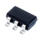
| 描述 | IC HS MOSFET DRIVER SOT-23-5门驱动器 2A HS Non-Invert |
| 产品分类 | PMIC - MOSFET,电桥驱动器 - 外部开关集成电路 - IC |
| 品牌 | Texas Instruments |
| 产品手册 | |
| 产品图片 |
|
| rohs | 符合RoHS无铅 / 符合限制有害物质指令(RoHS)规范要求 |
| 产品系列 | 电源管理 IC,门驱动器,Texas Instruments TPS2829DBVR- |
| 数据手册 | |
| 产品型号 | TPS2829DBVR |
| PCN设计/规格 | |
| 上升时间 | 14 ns |
| 下降时间 | 14 ns |
| 产品 | MOSFET Gate Drivers |
| 产品目录页面 | |
| 产品种类 | 门驱动器 |
| 供应商器件封装 | SOT-23-5 |
| 其它名称 | 296-1987-6 |
| 包装 | Digi-Reel® |
| 商标 | Texas Instruments |
| 安装类型 | 表面贴装 |
| 安装风格 | SMD/SMT |
| 封装 | Reel |
| 封装/外壳 | SC-74A,SOT-753 |
| 封装/箱体 | SOT-23-5 |
| 工作温度 | -40°C ~ 125°C |
| 工厂包装数量 | 3000 |
| 延迟时间 | 24ns |
| 最大功率耗散 | 437 mW |
| 最大工作温度 | + 125 C |
| 最小工作温度 | - 40 C |
| 标准包装 | 1 |
| 激励器数量 | 1 Driver |
| 电压-电源 | 4 V ~ 14 V |
| 电流-峰值 | 2A |
| 电源电压-最大 | 14 V |
| 电源电压-最小 | 4 V |
| 电源电流 | 15 mA |
| 类型 | MOSFET Driver |
| 系列 | TPS2829 |
| 输入类型 | 非反相 |
| 输出数 | 1 |
| 输出电流 | 2 A |
| 输出端数量 | 1 |
| 配置 | 低端 |
| 配置数 | 1 |
| 高压侧电压-最大值(自举) | - |


- 商务部:美国ITC正式对集成电路等产品启动337调查
- 曝三星4nm工艺存在良率问题 高通将骁龙8 Gen1或转产台积电
- 太阳诱电将投资9.5亿元在常州建新厂生产MLCC 预计2023年完工
- 英特尔发布欧洲新工厂建设计划 深化IDM 2.0 战略
- 台积电先进制程称霸业界 有大客户加持明年业绩稳了
- 达到5530亿美元!SIA预计今年全球半导体销售额将创下新高
- 英特尔拟将自动驾驶子公司Mobileye上市 估值或超500亿美元
- 三星加码芯片和SET,合并消费电子和移动部门,撤换高东真等 CEO
- 三星电子宣布重大人事变动 还合并消费电子和移动部门
- 海关总署:前11个月进口集成电路产品价值2.52万亿元 增长14.8%


PDF Datasheet 数据手册内容提取
(cid:1)(cid:2)(cid:3)(cid:4)(cid:5)(cid:6)(cid:7)(cid:8) (cid:1)(cid:2)(cid:3)(cid:4)(cid:5)(cid:6)(cid:10)(cid:8) (cid:1)(cid:2)(cid:3)(cid:4)(cid:5)(cid:6)(cid:5)(cid:8) (cid:1)(cid:2)(cid:3)(cid:4)(cid:5)(cid:6)(cid:11)(cid:8) (cid:1)(cid:2)(cid:3)(cid:4)(cid:5)(cid:4)(cid:5)(cid:8) (cid:1)(cid:2)(cid:3)(cid:4)(cid:5)(cid:4)(cid:11)(cid:8) (cid:3)(cid:12)(cid:13)(cid:14)(cid:15)(cid:16)(cid:17)(cid:18)(cid:19)(cid:20)(cid:13)(cid:13)(cid:16)(cid:15) (cid:19)(cid:12)(cid:14)(cid:19)(cid:17)(cid:3)(cid:2)(cid:16)(cid:16)(cid:21) (cid:22)(cid:23)(cid:3)(cid:24)(cid:16)(cid:1) (cid:21)(cid:25)(cid:12)(cid:26)(cid:16)(cid:25) SLVS160C – FEBRUARY 1997 – REVISED OCTOBER 2002 (cid:1) Low-Cost Single-Channel High-Speed TPS2816, TPS2817 MOSFET Driver TPS2818, TPS2819 (cid:1) I ...15-µA Max (TPS2828, TPS2829) DBV PACKAGE CC (TOP VIEW) (cid:1) 25-ns Max Rise/Fall Times and 40-ns Max Propagation Delay...1-nF Load VDD 1 5 VCC (cid:1) 2-A Peak Output Current (cid:1) GND 2 4-V to 14-V Driver Supply Voltage Range; Internal Regulator Extends Range to 40 V (TPS2816, TPS2817, TPS2818, TPS2819) IN 3 4 OUT (cid:1) 5-pin SOT-23 Package (cid:1) –40°C to 125°C Ambient-Temperature TPS2828, TPS2829 DBV PACKAGE Operating Range (TOP VIEW) (cid:1) Highly Resistant to Latch-ups NC 1 5 VCC description GND 2 The TPS28xx single-channel high-speed MOS- FET drivers are capable of delivering peak IN 3 4 OUT currents of up to 2 A into highly capacitive loads. High switching speeds (tr and tf = 14 ns typ) are NC – No internal connection obtained with the use of BiCMOS outputs. Typical threshold switching voltages are 2/3 and 1/3 of V . The design inherently minimizes shoot- CC through current. A regulator is provided on TPS2816 through TPS2819 devices to allow operation with supply inputs between 14 V and 40 V. The regulator output can be used to power other circuits, provided power dissipation does not exceed package limitations. If the regulator is not required, V (the regulator input) should be connected to DD V . The TPS2816 and TPS2817 input circuits include an active pullup circuit to eliminate the need for an CC external resistor when using open-collector PWM controllers. The TPS2818 and TPS2819 are identical to the TPS2816 and TPS2817, except that the active pullup circuit is omitted. The TPS2828 and TPS2829 are identical to the TPS2818 and TPS2819, except that the internal voltage regulator is omitted, allowing quiescent current to drop to less than 15 µA when the inputs are high or low. The TPS28xx series devices are available in 5-pin SOT-23 (DBV) packages and operate over an ambient temperature range of –40(cid:2)C to 125(cid:2)C. AVAILABLE OPTIONS PACKAGED DEVICES CCHHIIPP FFOORRMM TTA FFUUNNCCTTIIOONN SOT-23–5 (DBV) (Y) Inverting driver with active pullup input TPS2816DBV TPS2816Y Noninverting driver with active pullup input TPS2817DBV TPS2817Y Inverting driver TPS2818DBV TPS2818Y –4400°°CC ttoo 112255°°CC Noninverting driver TPS2819DBV TPS2819Y Inverting driver, no regulator TPS2828DBV TPS2828Y Noninverting driver, no regulator TPS2829DBV TPS2829Y The DBV package is available taped and reeled only. Please be aware that an important notice concerning availability, standard warranty, and use in critical applications of TexasInstruments semiconductor products and disclaimers thereto appears at the end of this data sheet. (cid:2)(cid:25)(cid:23)(cid:21)(cid:27)(cid:18)(cid:1)(cid:12)(cid:23)(cid:13) (cid:21)(cid:20)(cid:1)(cid:20) (cid:28)(cid:29)(cid:30)(cid:31) !"#(cid:28)(cid:31)(cid:29) (cid:28)$ %& ’(cid:29)# "$ (cid:31)(cid:30) (&)*(cid:28)%"#(cid:28)(cid:31)(cid:29) +"#’, Copyright 2002, Texas Instruments Incorporated (cid:2) (cid:31)+&%#$ %(cid:31)(cid:29)(cid:30)(cid:31) ! #(cid:31) $(’%(cid:28)(cid:30)(cid:28)%"#(cid:28)(cid:31)(cid:29)$ (’ #-’ #’ !$ (cid:31)(cid:30) (cid:1)’."$ (cid:12)(cid:29)$# &!’(cid:29)#$ $#"(cid:29)+" + /" "(cid:29)#0, (cid:2) (cid:31)+&%#(cid:28)(cid:31)(cid:29) ( (cid:31)%’$$(cid:28)(cid:29)1 +(cid:31)’$ (cid:29)(cid:31)# (cid:29)’%’$$" (cid:28)*0 (cid:28)(cid:29)%*&+’ #’$#(cid:28)(cid:29)1 (cid:31)(cid:30) "** (" "!’#’ $, www.ti.com 1
(cid:1)(cid:2)(cid:3)(cid:4)(cid:5)(cid:6)(cid:7)(cid:8) (cid:1)(cid:2)(cid:3)(cid:4)(cid:5)(cid:6)(cid:10)(cid:8) (cid:1)(cid:2)(cid:3)(cid:4)(cid:5)(cid:6)(cid:5)(cid:8) (cid:1)(cid:2)(cid:3)(cid:4)(cid:5)(cid:6)(cid:11)(cid:8) (cid:1)(cid:2)(cid:3)(cid:4)(cid:5)(cid:4)(cid:5)(cid:8) (cid:1)(cid:2)(cid:3)(cid:4)(cid:5)(cid:4)(cid:11)(cid:8) (cid:3)(cid:12)(cid:13)(cid:14)(cid:15)(cid:16)(cid:17)(cid:18)(cid:19)(cid:20)(cid:13)(cid:13)(cid:16)(cid:15) (cid:19)(cid:12)(cid:14)(cid:19)(cid:17)(cid:3)(cid:2)(cid:16)(cid:16)(cid:21) (cid:22)(cid:23)(cid:3)(cid:24)(cid:16)(cid:1) (cid:21)(cid:25)(cid:12)(cid:26)(cid:16)(cid:25) SLVS160C – FEBRUARY 1997 – REVISED OCTOBER 2002 functional block diagram TPS2816, TPS2818 TPS2817, TPS2819 VDD VREG VCC VDD VREG VCC Active Pullup Active Pullup (TPS2816 Only) (TPS2817 Only) IN OUT IN OUT GND GND TPS2828 TPS2829 VCC VCC IN OUT IN OUT GND GND INPUT STAGE DIAGRAM OUTPUT STAGE DIAGRAM VCC VCC Predrive To Drive IN Stage OUT 2 www.ti.com
(cid:1)(cid:2)(cid:3)(cid:4)(cid:5)(cid:6)(cid:7)(cid:8) (cid:1)(cid:2)(cid:3)(cid:4)(cid:5)(cid:6)(cid:10)(cid:8) (cid:1)(cid:2)(cid:3)(cid:4)(cid:5)(cid:6)(cid:5)(cid:8) (cid:1)(cid:2)(cid:3)(cid:4)(cid:5)(cid:6)(cid:11)(cid:8) (cid:1)(cid:2)(cid:3)(cid:4)(cid:5)(cid:4)(cid:5)(cid:8) (cid:1)(cid:2)(cid:3)(cid:4)(cid:5)(cid:4)(cid:11)(cid:8) (cid:3)(cid:12)(cid:13)(cid:14)(cid:15)(cid:16)(cid:17)(cid:18)(cid:19)(cid:20)(cid:13)(cid:13)(cid:16)(cid:15) (cid:19)(cid:12)(cid:14)(cid:19)(cid:17)(cid:3)(cid:2)(cid:16)(cid:16)(cid:21) (cid:22)(cid:23)(cid:3)(cid:24)(cid:16)(cid:1) (cid:21)(cid:25)(cid:12)(cid:26)(cid:16)(cid:25) SLVS160C – FEBRUARY 1997 – REVISED OCTOBER 2002 TPS28xxY chip information This chip, when properly assembled, displays characteristics similar to those of the TPS28xx. Thermal compression or ultrasonic bonding may be used on the doped aluminum bonding pads. The chip may be mounted with conductive epoxy or a gold-silicon preform. BONDING PAD ASSIGNMENTS (4) (5) (4) (5) OUT VCC (2) GND TPS2816Y (3) (1) IN VDD† 39 (2) †TPS2816 through TPS2819 only CHIP THICKNESS: 15 TYPICAL BONDING PADS: 4 × 4 MINIMUM TJ max = 150°C TOLERANCES ARE ±10%. (3) (1) ALL DIMENSIONS ARE IN MILS. 39 Terminal Functions TPS2816, TPS2818, TPS2828 (inverting driver) TERMINAL DDEESSCCRRIIPPTTIIOONN NAME NO. VDD 1 Regulator supply voltage input. (Not connected on TPS2828) GND 2 Ground IN 3 Driver input. OUT 4 Driver output, OUT = IN VCC 5 Driver supply voltage/regulator output voltage TPS2817, TPS2819, TPS2829 (noninverting driver) TERMINAL DDEESSCCRRIIPPTTIIOONN NAME NO. VDD 1 Regulator supply voltage input. (Not connected on TPS2829) GND 2 Ground IN 3 Driver input. OUT 4 Driver output, OUT= IN VCC 5 Driver supply voltage/regulator output voltage www.ti.com 3
(cid:1)(cid:2)(cid:3)(cid:4)(cid:5)(cid:6)(cid:7)(cid:8) (cid:1)(cid:2)(cid:3)(cid:4)(cid:5)(cid:6)(cid:10)(cid:8) (cid:1)(cid:2)(cid:3)(cid:4)(cid:5)(cid:6)(cid:5)(cid:8) (cid:1)(cid:2)(cid:3)(cid:4)(cid:5)(cid:6)(cid:11)(cid:8) (cid:1)(cid:2)(cid:3)(cid:4)(cid:5)(cid:4)(cid:5)(cid:8) (cid:1)(cid:2)(cid:3)(cid:4)(cid:5)(cid:4)(cid:11)(cid:8) (cid:3)(cid:12)(cid:13)(cid:14)(cid:15)(cid:16)(cid:17)(cid:18)(cid:19)(cid:20)(cid:13)(cid:13)(cid:16)(cid:15) (cid:19)(cid:12)(cid:14)(cid:19)(cid:17)(cid:3)(cid:2)(cid:16)(cid:16)(cid:21) (cid:22)(cid:23)(cid:3)(cid:24)(cid:16)(cid:1) (cid:21)(cid:25)(cid:12)(cid:26)(cid:16)(cid:25) SLVS160C – FEBRUARY 1997 – REVISED OCTOBER 2002 DISSIPATION RATING TABLE TA ≤ 25°C DERATING FACTOR TA = 70°C TA = 80°C PACKAGE POWER RATING ABOVE TA = 25°C POWER RATING POWER RATING DBV 437 mW 3.5 mW/°C 280 mW 227 mW These dissipation ratings are based upon EIA specification JESD51-3, ”Low Effective Thermal Conductivity Test Board for Leaded Surface Mount Packages,” in tests conducted in a zero-airflow, wind tunnel environment. absolute maximum ratings over operating temperature range (unless otherwise noted)† Supply voltage range, V . . . . . . . . . . . . . . . . . . . . . . . . . . . . . . . . . . . . . . . . . . . . . . . . . . . . . . . . . –0.3 V to 15 V CC Regulator supply voltage range, V . . . . . . . . . . . . . . . . . . . . . . . . . . . . . . . . . . . . . . . . . . . . V –0.3 V to 42 V DD CC Input voltage range, IN . . . . . . . . . . . . . . . . . . . . . . . . . . . . . . . . . . . . . . . . . . . . . . . . . . . . . . –0.3 V to V +0.5 V CC Output voltage range, (pin 4) . . . . . . . . . . . . . . . . . . . . . . . . . . . . . . . . . . . . . . . . . . . . . . . . . –0.5 V to V +0.5 V CC Continuous regulator output current, V . . . . . . . . . . . . . . . . . . . . . . . . . . . . . . . . . . . . . . . . . . . . . . . . . . . . 25 mA CC Continuous output current, OUT . . . . . . . . . . . . . . . . . . . . . . . . . . . . . . . . . . . . . . . . . . . . . . . . . . . . . . . . . ±100 mA Continuous total power dissipation . . . . . . . . . . . . . . . . . . . . . . . . . . . . . . . . . . . . . See Dissipation Rating Table Operating ambient temperature range, T . . . . . . . . . . . . . . . . . . . . . . . . . . . . . . . . . . . –40°C to 125°C A Storage temperature range, T . . . . . . . . . . . . . . . . . . . . . . . . . . . . . . . . . . . . . . . . . . –65°C to 150°C stg Lead temperature 1,6 mm (1/16inch) from case for 10 seconds . . . . . . . . . . . . . . . . . . . . . . . . . . . . . . . . . 260°C †Stresses beyond those listed under “absolute maximum ratings” may cause permanent damage to the device. These are stress ratings only, and functional operation of the device at these or any other conditions beyond those indicated under “recommended operating conditions” is not implied. Exposure to absolute-maximum-rated conditions for extended periods may affect device reliability. NOTE 1: All voltages are with respect to device GND terminal. recommended operating conditions MIN MAX UNIT Regulator input voltage range, VDD, TPS2816 through TPS2819 8 40 V Supply voltage, VCC 4 14 V Input voltage, IN –0.3 VCC V Continuous regulator output current, ICC 0 20 mA Operating ambient temperature range, TA –40 125 (cid:2)C 4 www.ti.com
(cid:1)(cid:2)(cid:3)(cid:4)(cid:5)(cid:6)(cid:7)(cid:8) (cid:1)(cid:2)(cid:3)(cid:4)(cid:5)(cid:6)(cid:10)(cid:8) (cid:1)(cid:2)(cid:3)(cid:4)(cid:5)(cid:6)(cid:5)(cid:8) (cid:1)(cid:2)(cid:3)(cid:4)(cid:5)(cid:6)(cid:11)(cid:8) (cid:1)(cid:2)(cid:3)(cid:4)(cid:5)(cid:4)(cid:5)(cid:8) (cid:1)(cid:2)(cid:3)(cid:4)(cid:5)(cid:4)(cid:11)(cid:8) (cid:3)(cid:12)(cid:13)(cid:14)(cid:15)(cid:16)(cid:17)(cid:18)(cid:19)(cid:20)(cid:13)(cid:13)(cid:16)(cid:15) (cid:19)(cid:12)(cid:14)(cid:19)(cid:17)(cid:3)(cid:2)(cid:16)(cid:16)(cid:21) (cid:22)(cid:23)(cid:3)(cid:24)(cid:16)(cid:1) (cid:21)(cid:25)(cid:12)(cid:26)(cid:16)(cid:25) SLVS160C – FEBRUARY 1997 – REVISED OCTOBER 2002 TPS28xx electrical characteristics over recommended operating ambient temperature range, V = 10 V, V tied to V , C = 1 nF (unless otherwise specified) CC DD CC L Inputs PARAMETER TEST CONDITIONS MIN TYP† MAX UNIT VCC = 5 V 3.3 4 PPoossiittiivvee-ggooiinngg iinnpuutt tthhrreesshhoolldd vvoollttaaggee VCC = 10 V 6.6 7 VV VCC = 14 V 9.3 10 VCC = 5 V 1 1.7 NNeeggaattiivvee-ggooiinngg iinnpuutt tthhrreesshhoolldd vvoollttaaggee VCC = 10 V 2 3.3 VV VCC = 14 V 2.5 4.6 Input voltage hysteresis 1.3 V Input current, TPS2818/19/28/29 Input = 0 V or VCC 0.2 µA Input = 0 V 650 IInnppuutt ccuurrrreenntt, TTPPSS22881166//1177 µAA Input = VCC 15 Input capacitance 5 10 pF †Typicals are for TA = 25°C unless otherwise noted. outputs PARAMETER TEST CONDITIONS MIN TYP† MAX UNIT IO = –1 mA 9.75 9.9 HHiighh-llevell outtputt vollttage VV IO = –100 mA 8 9.1 IO = 1 mA 0.18 0.25 LLoow-lleeveell oouttpputt voollttaaggee VV IO = 100 mA 1 2 †Typicals are for TA = 25°C unless otherwise noted. regulator, TPS2816 through TPS2819 PARAMETER TEST CONDITIONS MIN TYP† MAX UNIT 1144 ≤≤ VVDDDD ≤≤ 4400 VV,, 1100 1111..55 1133 OOuttpputt voollttaaggee 0 ≤ IO ≤ 20 mA VV IIOO = 1100 mmAA,, 88 1100 OOuuttppuutt vvoollttaaggee iinn ddrrooppoouutt VV VDD = 10 V †Typicals are for TA = 25°C unless otherwise noted. supply current PARAMETER TEST CONDITIONS MIN TYP† MAX UNIT TTPPSS22881166,, IN = high = 10 V 150 250 TPS2817 IN = low = 0 V 650 1000 SSuuppppllyy ccuurrrreenntt iinnttoo VVCCCC TTPPSS22881188,, 2255 5500 µµAA TPS2819 IINN == hhiigghh oorr llooww,, TPS2828, High = 10 V, Low = 0 V 0.1 15 TPS2829 TTPPSS22881166,, VVDDDD == 2200 VV,, 665500 11000000 TPS2817 IN = high = 10 V or low = 0 V SSuuppppllyy ccuurrrreenntt iinnttoo VVDDDD µµAA TTPPSS22881188,, VVDDDD == 2200 VV,, 5500 115500 TPS2819 IN = high = 10 V or low = 0 V †Typicals are for TA = 25°C unless otherwise noted. www.ti.com 5
(cid:1)(cid:2)(cid:3)(cid:4)(cid:5)(cid:6)(cid:7)(cid:8) (cid:1)(cid:2)(cid:3)(cid:4)(cid:5)(cid:6)(cid:10)(cid:8) (cid:1)(cid:2)(cid:3)(cid:4)(cid:5)(cid:6)(cid:5)(cid:8) (cid:1)(cid:2)(cid:3)(cid:4)(cid:5)(cid:6)(cid:11)(cid:8) (cid:1)(cid:2)(cid:3)(cid:4)(cid:5)(cid:4)(cid:5)(cid:8) (cid:1)(cid:2)(cid:3)(cid:4)(cid:5)(cid:4)(cid:11)(cid:8) (cid:3)(cid:12)(cid:13)(cid:14)(cid:15)(cid:16)(cid:17)(cid:18)(cid:19)(cid:20)(cid:13)(cid:13)(cid:16)(cid:15) (cid:19)(cid:12)(cid:14)(cid:19)(cid:17)(cid:3)(cid:2)(cid:16)(cid:16)(cid:21) (cid:22)(cid:23)(cid:3)(cid:24)(cid:16)(cid:1) (cid:21)(cid:25)(cid:12)(cid:26)(cid:16)(cid:25) SLVS160C – FEBRUARY 1997 – REVISED OCTOBER 2002 TPS28xxY electrical characteristics at TA = 25(cid:2)C, VCC = 10 V, VDD tied to VCC, CL = 1 nF (unless otherwise specified) Inputs PARAMETER TEST CONDITIONS MIN TYP MAX UNIT VCC = 5 V 3.3 PPoossiittiivvee-ggooiinngg iinnpuutt tthhrreesshhoolldd vvoollttaaggee VCC = 10 V 6.6 VV VCC = 14 V 9.3 VCC = 5 V 1.7 NNeeggaattiivvee-ggooiinngg iinnpuutt tthhrreesshhoolldd vvoollttaaggee VCC = 10 V 3.3 VV VCC = 14 V 4.6 Input voltage hysteresis 1.3 V Input current, TPS2818/19/28/29 Input = 0 V or VCC 0.2 µA Input = 0 V 650 IInnppuutt ccuurrrreenntt, TTPPSS22881166//1177 µAA Input = VCC 15 Input resistance 1000 MΩ Input capacitance 5 pF outputs PARAMETER TEST CONDITIONS MIN TYP MAX UNIT IO = –1 mA 9.9 HHiighh-llevell outtputt vollttage VV IO = –100 mA 9.1 IO = 1 mA 0.18 LLooww-lleevveell oouuttppuutt vvoollttaaggee VV IO = 100 mA 1 regulator, TPS2816 through TPS2819 PARAMETER TEST CONDITIONS MIN TYP MAX UNIT Output voltage 14 ≤ VDD ≤ 40 V, 11.5 V 0 ≤ IO ≤ 20 mA Output voltage in dropout IO = 10 mA, 9 V VDD = 10 V supply current PARAMETER TEST CONDITIONS MIN TYP MAX UNIT TTPPSS22881166,, IN = high = 10 V 150 TPS2817 IN = low = 0 V 650 SSuuppppllyy ccuurrrreenntt iinnttoo VVCCCC TTPPSS22881188,, 2255 µµAA TPS2819 IINN == hhiigghh oorr llooww,, TPS2828, High = 10 V, Low = 0 V 0.1 TPS2829 TTPPSS22881166,, VVDDDD == 2200 VV,, 665500 TPS2817 IN = high = 10 V or low = 0 V SSuuppppllyy ccuurrrreenntt iinnttoo VVDDDD µµAA TTPPSS22881188,, VVDDDD == 2200 VV,, 5500 TPS2819 IN = high = 10 V or low = 0 V 6 www.ti.com
(cid:1)(cid:2)(cid:3)(cid:4)(cid:5)(cid:6)(cid:7)(cid:8) (cid:1)(cid:2)(cid:3)(cid:4)(cid:5)(cid:6)(cid:10)(cid:8) (cid:1)(cid:2)(cid:3)(cid:4)(cid:5)(cid:6)(cid:5)(cid:8) (cid:1)(cid:2)(cid:3)(cid:4)(cid:5)(cid:6)(cid:11)(cid:8) (cid:1)(cid:2)(cid:3)(cid:4)(cid:5)(cid:4)(cid:5)(cid:8) (cid:1)(cid:2)(cid:3)(cid:4)(cid:5)(cid:4)(cid:11)(cid:8) (cid:3)(cid:12)(cid:13)(cid:14)(cid:15)(cid:16)(cid:17)(cid:18)(cid:19)(cid:20)(cid:13)(cid:13)(cid:16)(cid:15) (cid:19)(cid:12)(cid:14)(cid:19)(cid:17)(cid:3)(cid:2)(cid:16)(cid:16)(cid:21) (cid:22)(cid:23)(cid:3)(cid:24)(cid:16)(cid:1) (cid:21)(cid:25)(cid:12)(cid:26)(cid:16)(cid:25) SLVS160C – FEBRUARY 1997 – REVISED OCTOBER 2002 switching characteristics for all devices over recommended operating ambient temperature range, V = 10 V, V tied to V , C = 1 nF (unless otherwise specified) CC DD CC L PARAMETER TEST CONDITIONS MIN TYP MAX UNIT VCC = 14 V 25 trr Rise time VCC = 10 V 14 30 ns VCC = 5 V 35 VCC = 14 V 25 tff Fall time VCC = 10 V 14 30 ns VCC = 5 V 35 VCC = 14 V 40 tPPHHLL Propaggation delayy time,, higgh-to-low-level output VCC = 10 V 24 45 ns VCC = 5 V 50 VCC = 14 V 40 tPPLLHH Propaggation delayy time,, low-to-higgh-level output VCC = 10 V 24 45 ns VCC = 5 V 50 PARAMETER MEASUREMENT INFORMATION IN 50% 50% 0 V tf tr 90% 90% OUT 50% 50% 10% 10% 0 V tPHL tPLH Figure 1. Typical Timing Diagram (TPS2816) www.ti.com 7
(cid:1)(cid:2)(cid:3)(cid:4)(cid:5)(cid:6)(cid:7)(cid:8) (cid:1)(cid:2)(cid:3)(cid:4)(cid:5)(cid:6)(cid:10)(cid:8) (cid:1)(cid:2)(cid:3)(cid:4)(cid:5)(cid:6)(cid:5)(cid:8) (cid:1)(cid:2)(cid:3)(cid:4)(cid:5)(cid:6)(cid:11)(cid:8) (cid:1)(cid:2)(cid:3)(cid:4)(cid:5)(cid:4)(cid:5)(cid:8) (cid:1)(cid:2)(cid:3)(cid:4)(cid:5)(cid:4)(cid:11)(cid:8) (cid:3)(cid:12)(cid:13)(cid:14)(cid:15)(cid:16)(cid:17)(cid:18)(cid:19)(cid:20)(cid:13)(cid:13)(cid:16)(cid:15) (cid:19)(cid:12)(cid:14)(cid:19)(cid:17)(cid:3)(cid:2)(cid:16)(cid:16)(cid:21) (cid:22)(cid:23)(cid:3)(cid:24)(cid:16)(cid:1) (cid:21)(cid:25)(cid:12)(cid:26)(cid:16)(cid:25) SLVS160C – FEBRUARY 1997 – REVISED OCTOBER 2002 PARAMETER MEASUREMENT INFORMATION TPS2816 1 5 Regulator 10 V 0.1 µF + 4.7 µF 2 3 4 Input Output 50 Ω 1 nF Figure 2. Switching Time Test Setup TPS2816 Current Loop VCC 10 V + 0.1 µF 4.7 µF 0–10 Vdc OUT Figure 3. Shoot-Through Current Test Setup 8 www.ti.com
(cid:1)(cid:2)(cid:3)(cid:4)(cid:5)(cid:6)(cid:7)(cid:8) (cid:1)(cid:2)(cid:3)(cid:4)(cid:5)(cid:6)(cid:10)(cid:8) (cid:1)(cid:2)(cid:3)(cid:4)(cid:5)(cid:6)(cid:5)(cid:8) (cid:1)(cid:2)(cid:3)(cid:4)(cid:5)(cid:6)(cid:11)(cid:8) (cid:1)(cid:2)(cid:3)(cid:4)(cid:5)(cid:4)(cid:5)(cid:8) (cid:1)(cid:2)(cid:3)(cid:4)(cid:5)(cid:4)(cid:11)(cid:8) (cid:3)(cid:12)(cid:13)(cid:14)(cid:15)(cid:16)(cid:17)(cid:18)(cid:19)(cid:20)(cid:13)(cid:13)(cid:16)(cid:15) (cid:19)(cid:12)(cid:14)(cid:19)(cid:17)(cid:3)(cid:2)(cid:16)(cid:16)(cid:21) (cid:22)(cid:23)(cid:3)(cid:24)(cid:16)(cid:1) (cid:21)(cid:25)(cid:12)(cid:26)(cid:16)(cid:25) SLVS160C – FEBRUARY 1997 – REVISED OCTOBER 2002 TYPICAL CHARACTERISTICS Table of Graphs FIGURE Rise time vs Supply voltage 4 Fall time vs Supply voltage 5 Propagation time (L>H) vs Supply voltage 6 Propagation Time (H>L) vs Supply voltage 7 Rise time vs Ambient temperature 8 Fall time vs Ambient temperature 9 Propagation time (L>H) vs Supply voltage 10 Propagation time (H>L) vs Ambient temperature 11 Supply current (VCC) vs Supply voltage 12 Supply current (VCC) vs Load capacitance 13 Supply current (VCC) vs Ambient temperature 14 Input threshold voltage vs Supply voltage 15 Regulator output voltage vs Regulator supply voltage 16 Regulator quiescent current vs Regulator supply voltage 17 Shoot-through current vs Input voltage (L>H) 18 Shoot-through current vs Input voltage (H>L) 19 www.ti.com 9
(cid:1)(cid:2)(cid:3)(cid:4)(cid:5)(cid:6)(cid:7)(cid:8) (cid:1)(cid:2)(cid:3)(cid:4)(cid:5)(cid:6)(cid:10)(cid:8) (cid:1)(cid:2)(cid:3)(cid:4)(cid:5)(cid:6)(cid:5)(cid:8) (cid:1)(cid:2)(cid:3)(cid:4)(cid:5)(cid:6)(cid:11)(cid:8) (cid:1)(cid:2)(cid:3)(cid:4)(cid:5)(cid:4)(cid:5)(cid:8) (cid:1)(cid:2)(cid:3)(cid:4)(cid:5)(cid:4)(cid:11)(cid:8) (cid:3)(cid:12)(cid:13)(cid:14)(cid:15)(cid:16)(cid:17)(cid:18)(cid:19)(cid:20)(cid:13)(cid:13)(cid:16)(cid:15) (cid:19)(cid:12)(cid:14)(cid:19)(cid:17)(cid:3)(cid:2)(cid:16)(cid:16)(cid:21) (cid:22)(cid:23)(cid:3)(cid:24)(cid:16)(cid:1) (cid:21)(cid:25)(cid:12)(cid:26)(cid:16)(cid:25) SLVS160C – FEBRUARY 1997 – REVISED OCTOBER 2002 TYPICAL CHARACTERISTICS RISE TIME FALL TIME vs vs SUPPLY VOLTAGE SUPPLY VOLTAGE 35 30 TA = 25°C TA = 25°C 30 25 CL = 2200 pF 25 ns CL = 2200 pF ns 20 me – 20 me – Ti Ti 15 Rise 15 Fall – – tr CL = 1000 pF tf 10 CL = 1000 pF 10 5 5 CL = 0 CL = 0 0 0 4 6 8 10 12 14 4 6 8 10 12 14 VCC – Supply Voltage – V VCC – Supply Voltage – V Figure 4 Figure 5 PROPAGATION DELAY TIME, PROPAGATION DELAY TIME, LOW-TO-HIGH-LEVEL OUTPUT HIGH-TO-LOW-LEVEL OUTPUT vs vs SUPPLY VOLTAGE SUPPLY VOLTAGE 40 40 TA = 25°C TA = 25°C 35 35 Propagation Delay Time, t –PLHLow-To-High-Level Output – ns 2123105500 CCLL =C = L2 1 2=00 0000 p pFF Propagation Delay Time,t –PHLHigh-To-Low-Level Output – ns 2123105500 CCLL = = 1C 02L02 00= 0 p0 pFF 5 5 0 0 4 6 8 10 12 14 4 6 8 10 12 14 VCC – Supply Voltage – V VCC – Supply Voltage – V Figure 6 Figure 7 10 www.ti.com
(cid:1)(cid:2)(cid:3)(cid:4)(cid:5)(cid:6)(cid:7)(cid:8) (cid:1)(cid:2)(cid:3)(cid:4)(cid:5)(cid:6)(cid:10)(cid:8) (cid:1)(cid:2)(cid:3)(cid:4)(cid:5)(cid:6)(cid:5)(cid:8) (cid:1)(cid:2)(cid:3)(cid:4)(cid:5)(cid:6)(cid:11)(cid:8) (cid:1)(cid:2)(cid:3)(cid:4)(cid:5)(cid:4)(cid:5)(cid:8) (cid:1)(cid:2)(cid:3)(cid:4)(cid:5)(cid:4)(cid:11)(cid:8) (cid:3)(cid:12)(cid:13)(cid:14)(cid:15)(cid:16)(cid:17)(cid:18)(cid:19)(cid:20)(cid:13)(cid:13)(cid:16)(cid:15) (cid:19)(cid:12)(cid:14)(cid:19)(cid:17)(cid:3)(cid:2)(cid:16)(cid:16)(cid:21) (cid:22)(cid:23)(cid:3)(cid:24)(cid:16)(cid:1) (cid:21)(cid:25)(cid:12)(cid:26)(cid:16)(cid:25) SLVS160C – FEBRUARY 1997 – REVISED OCTOBER 2002 TYPICAL CHARACTERISTICS RISE TIME FALL TIME vs vs AMBIENT TEMPERATURE AMBIENT TEMPERATURE 19 20 VCC = 10 V VCC = 10 V 19 Load = 1000 pF Load = 1000 pF 18 f = 100 kHz f = 100 kHz 18 17 17 Time – ns 16 Time – ns 1156 Rise Fall 14 – tr 15 – tf 13 12 14 11 13 10 –50 –25 0 25 50 75 100 125 –50 –25 0 25 50 75 100 125 Ambient Temperature – °C Ambient Temperature – °C Figure 8 Figure 9 PROPAGATION DELAY TIME, PROPAGATION DELAY TIME, LOW-TO-HIGH-LEVEL OUTPUT HIGH-TO-LOW-LEVEL OUTPUT vs vs SUPPLY VOLTAGE AMBIENT TEMPERATURE 19 20 VCC = 10 V VCC = 10 V Load = 1000 pF 19 Load = 1000 pF Propagation Delay Time, t –PLHLow-To-High-Level Output – ns 1111165478 f = 100 kHz Propagation Delay Time,t –PHLHigh-To-Low-Level Output – ns 11111118635427 f = 100 kHz 11 13 10 –50 –25 0 25 50 75 100 125 –50 –25 0 25 50 75 100 125 TA – Ambient Temperature – °C TA – Ambient Temperature – °C Figure 10 Figure 11 www.ti.com 11
(cid:1)(cid:2)(cid:3)(cid:4)(cid:5)(cid:6)(cid:7)(cid:8) (cid:1)(cid:2)(cid:3)(cid:4)(cid:5)(cid:6)(cid:10)(cid:8) (cid:1)(cid:2)(cid:3)(cid:4)(cid:5)(cid:6)(cid:5)(cid:8) (cid:1)(cid:2)(cid:3)(cid:4)(cid:5)(cid:6)(cid:11)(cid:8) (cid:1)(cid:2)(cid:3)(cid:4)(cid:5)(cid:4)(cid:5)(cid:8) (cid:1)(cid:2)(cid:3)(cid:4)(cid:5)(cid:4)(cid:11)(cid:8) (cid:3)(cid:12)(cid:13)(cid:14)(cid:15)(cid:16)(cid:17)(cid:18)(cid:19)(cid:20)(cid:13)(cid:13)(cid:16)(cid:15) (cid:19)(cid:12)(cid:14)(cid:19)(cid:17)(cid:3)(cid:2)(cid:16)(cid:16)(cid:21) (cid:22)(cid:23)(cid:3)(cid:24)(cid:16)(cid:1) (cid:21)(cid:25)(cid:12)(cid:26)(cid:16)(cid:25) SLVS160C – FEBRUARY 1997 – REVISED OCTOBER 2002 TYPICAL CHARACTERISTICS SUPPLY CURRENT SUPPLY CURRENT vs vs SUPPLY VOLTAGE LOAD CAPACITANCE 16 4 Load = 1000 pF VCC = 10 V f = 100 kHz 14 Duty Cycle = 50% 3.5 Duty Cycle = 50% A 12 f = 1 MHz mA 3 nt – m 10 ent – 2.5 urre Curr ply C 8 f = 500 kHz pply 2 p u u 6 S 1.5 – S – C C C C 4 I 1 I f = 40 kHz f = 100 kHz 2 0.5 0 0 4 6 8 10 12 14 0 1000 2000 VCC – Supply Voltage – V CL – Load Capacitance – pF Figure 12 Figure 13 SUPPLY CURRENT INPUT THRESHOLD VOLTAGE vs vs AMBIENT TEMPERATURE SUPPLY VOLTAGE 3 9 VCC = 10 V Load = 1000 pF 8 f = 100 kHz Duty Cycle = 50% A 2.5 V 7 m – ent – oltage 6 Positive Going ply Curr 2 shold V 54 p e Su Thr Negative Going – C ut 3 C 1.5 np I – I 2 T VI 1 1 0 –50 –25 0 25 50 75 100 125 4 6 8 10 12 14 TA – Ambient Temperature – °C VCC – Supply Voltage – V Figure 14 Figure 15 12 www.ti.com
(cid:1)(cid:2)(cid:3)(cid:4)(cid:5)(cid:6)(cid:7)(cid:8) (cid:1)(cid:2)(cid:3)(cid:4)(cid:5)(cid:6)(cid:10)(cid:8) (cid:1)(cid:2)(cid:3)(cid:4)(cid:5)(cid:6)(cid:5)(cid:8) (cid:1)(cid:2)(cid:3)(cid:4)(cid:5)(cid:6)(cid:11)(cid:8) (cid:1)(cid:2)(cid:3)(cid:4)(cid:5)(cid:4)(cid:5)(cid:8) (cid:1)(cid:2)(cid:3)(cid:4)(cid:5)(cid:4)(cid:11)(cid:8) (cid:3)(cid:12)(cid:13)(cid:14)(cid:15)(cid:16)(cid:17)(cid:18)(cid:19)(cid:20)(cid:13)(cid:13)(cid:16)(cid:15) (cid:19)(cid:12)(cid:14)(cid:19)(cid:17)(cid:3)(cid:2)(cid:16)(cid:16)(cid:21) (cid:22)(cid:23)(cid:3)(cid:24)(cid:16)(cid:1) (cid:21)(cid:25)(cid:12)(cid:26)(cid:16)(cid:25) SLVS160C – FEBRUARY 1997 – REVISED OCTOBER 2002 TYPICAL CHARACTERISTICS REGULATOR OUTPUT VOLTAGE REGULATOR QUIESCENT CURRENT vs vs REGULATOR SUPPLY VOLTAGE REGULATOR SUPPLY VOLTAGE 12 670 TPS2816,17 only 11 665 No Load A µ 660 V – 10 – ge nt 655 a e Volt 9 Curr 650 put 8 ent 645 Out esc Regulator 76 ulator Qui 663450 Load = 10 kΩ eg 630 R 5 625 4 620 4 8 12 16 20 24 28 32 36 40 4 8 12 16 20 24 28 32 36 40 VDD – Regulator Supply Voltage – V VDD – Regulator Supply Voltage – V Figure 16 Figure 17 SHOOT-THROUGH CURRENT SHOOT-THROUGH CURRENT vs vs INPUT VOLTAGE LOW-TO-HIGH INPUT VOLTAGE HIGH-TO-LOW 7 7 VCC = 10 V VCC = 10 V No Load No Load 6 TA = 25°C 6 TA = 25°C A A Current – m 45 Current – m 45 Shoot-Through 32 Shoot-Through 32 1 1 0 0 0 2 4 6 8 10 0 2 4 6 8 10 VI – Input Voltage – V VI – Input Voltage – V Figure 18 Figure 19 www.ti.com 13
(cid:1)(cid:2)(cid:3)(cid:4)(cid:5)(cid:6)(cid:7)(cid:8) (cid:1)(cid:2)(cid:3)(cid:4)(cid:5)(cid:6)(cid:10)(cid:8) (cid:1)(cid:2)(cid:3)(cid:4)(cid:5)(cid:6)(cid:5)(cid:8) (cid:1)(cid:2)(cid:3)(cid:4)(cid:5)(cid:6)(cid:11)(cid:8) (cid:1)(cid:2)(cid:3)(cid:4)(cid:5)(cid:4)(cid:5)(cid:8) (cid:1)(cid:2)(cid:3)(cid:4)(cid:5)(cid:4)(cid:11)(cid:8) (cid:3)(cid:12)(cid:13)(cid:14)(cid:15)(cid:16)(cid:17)(cid:18)(cid:19)(cid:20)(cid:13)(cid:13)(cid:16)(cid:15) (cid:19)(cid:12)(cid:14)(cid:19)(cid:17)(cid:3)(cid:2)(cid:16)(cid:16)(cid:21) (cid:22)(cid:23)(cid:3)(cid:24)(cid:16)(cid:1) (cid:21)(cid:25)(cid:12)(cid:26)(cid:16)(cid:25) SLVS160C – FEBRUARY 1997 – REVISED OCTOBER 2002 APPLICATION INFORMATION MOSFETs are voltage-driven devices that require very little steady-state drive current. However, the large input capacitance (200 pF to 3000 pF or greater) of these devices requires large current surges to reduce the turn-on and turn-off times. The TPS2816 series of high-speed drivers can supply up to 2 A to a MOSFET, greatly reducing the switching times. The fast rise times and fall times and short propagation delays allow for operation in today’s high-frequency switching converters. In addition, MOSFETs have a limited gate-bias voltage range, usually less than 20 V. The TPS2816 series of drivers extends this operating range by incorporating an on-board series regulator with an input range up to 40 V. This regulator can be used to power the drivers, the PWM chip, and other circuitry, providing the power dissipation rating is not exceeded. When using these devices, care should be exercised in the proper placement of the driver, the switching MOSFET, and the bypass capacitor. Because of the large input capacitance of the MOSFET, the driver should be placed close to the gate to eliminate the possibility of oscillations caused by trace inductance ringing with the gate capacitance of the MOSFET. When the driver output path is longer than approximately 2 inches, a resistor in the range of 10 Ω should be placed in series with the gate drive as close as possible to the MOSFET. A ceramic bypass capacitor is also recommended to provide a source for the high-speed current transients that the MOSFET requires. This capacitor should be placed between V and GND of the driver (see Figures 20 CC and 21). TPS2816 VCC 1 5 Regulator Load 2 0.1 µF 3 4 Input Figure 20. V < 14 V CC TPS2816 VDD 1 5 Regulator + 0.1 µF 2 Load 4.7 µF 3 4 Input Figure 21. V > 14 V CC 14 www.ti.com
(cid:1)(cid:2)(cid:3)(cid:4)(cid:5)(cid:6)(cid:7)(cid:8) (cid:1)(cid:2)(cid:3)(cid:4)(cid:5)(cid:6)(cid:10)(cid:8) (cid:1)(cid:2)(cid:3)(cid:4)(cid:5)(cid:6)(cid:5)(cid:8) (cid:1)(cid:2)(cid:3)(cid:4)(cid:5)(cid:6)(cid:11)(cid:8) (cid:1)(cid:2)(cid:3)(cid:4)(cid:5)(cid:4)(cid:5)(cid:8) (cid:1)(cid:2)(cid:3)(cid:4)(cid:5)(cid:4)(cid:11)(cid:8) (cid:3)(cid:12)(cid:13)(cid:14)(cid:15)(cid:16)(cid:17)(cid:18)(cid:19)(cid:20)(cid:13)(cid:13)(cid:16)(cid:15) (cid:19)(cid:12)(cid:14)(cid:19)(cid:17)(cid:3)(cid:2)(cid:16)(cid:16)(cid:21) (cid:22)(cid:23)(cid:3)(cid:24)(cid:16)(cid:1) (cid:21)(cid:25)(cid:12)(cid:26)(cid:16)(cid:25) SLVS160C – FEBRUARY 1997 – REVISED OCTOBER 2002 APPLICATION INFORMATION The on-board series regulator supplies approximately 20 mA of current at 11.5 V, some of which can be used for external circuitry, providing the power dissipation rating for the driver is not exceeded. When using the on-board series regulator, an electrolytic output capacitor of 4.7 µF or larger is recommended. Although not required, a 0.1-µF ceramic capacitor on the input of the regulator can help suppress transient currents (see Figure 22). When not used, the regulator should be connected to V . Grounding V will result in destruction CC DD of the regulator. 34 VDC 0.1 µF + 0.1 µF 4.7 µF VCC TPS2816 PWM Controller 1 5 Regulator 0.1 µF 2 VO 3 4 Out 10 µF GND Figure 22. Boost Application The TPS2816 and TPS2818 drivers include active pullup circuits on the inputs to eliminate the need for external pullup resistors when using controllers with open-collector outputs (such as the TL5001). The TPS2817 and TPS2819 drivers have standard CMOS inputs providing a total device operating current of less than 50 µA. All devices switch at standard CMOS logic levels of approximately 2/3 V with positive-going input levels, and CC approximately 1/3 V with negative-going input levels. Being CMOS drivers, these devices will draw relatively CC large amounts of current (Approximately 5 mA) when the inputs are in the range of one-half of the supply voltage. In normal operation, the driver input is in this range for a very short time. Care should be taken to avoid use of very low slew-rate inputs, used under normal operating conditions. Although not destructive to the device, slew rates slower than 0.1 V/µs are not recommended. The BiCMOS output stage provides high instantaneous drive current to rapidly toggle the power switch, and very low drop to each rail to ensure proper operation at voltage extremes. Low-voltage circuits (less than 14 V) that require very low quiescent currents can use the TPS2828 and TPS2829 drivers. These drivers use typically 0.2 µA of quiescent current (with inputs high or low). They do not have the internal regulator or the active pullup circuit, but all other specifications are the same as for the rest of the family. 2.5-V/3.3-V, 3-A application Figure 23 illustrates the use of the TPS2817 with a TL5001 PWM controller and a TPS1110 in a simple step-down converter application. The converter operates at 275 kHz and delivers either 2.5 V or 3.3 V (determined by the value of R6) at 3 A (5 A peak) from a 5-V supply. The bill of materials is provided in Table 1. www.ti.com 15
(cid:1)(cid:2)(cid:3)(cid:4)(cid:5)(cid:6)(cid:7)(cid:8) (cid:1)(cid:2)(cid:3)(cid:4)(cid:5)(cid:6)(cid:10)(cid:8) (cid:1)(cid:2)(cid:3)(cid:4)(cid:5)(cid:6)(cid:5)(cid:8) (cid:1)(cid:2)(cid:3)(cid:4)(cid:5)(cid:6)(cid:11)(cid:8) (cid:1)(cid:2)(cid:3)(cid:4)(cid:5)(cid:4)(cid:5)(cid:8) (cid:1)(cid:2)(cid:3)(cid:4)(cid:5)(cid:4)(cid:11)(cid:8) (cid:3)(cid:12)(cid:13)(cid:14)(cid:15)(cid:16)(cid:17)(cid:18)(cid:19)(cid:20)(cid:13)(cid:13)(cid:16)(cid:15) (cid:19)(cid:12)(cid:14)(cid:19)(cid:17)(cid:3)(cid:2)(cid:16)(cid:16)(cid:21) (cid:22)(cid:23)(cid:3)(cid:24)(cid:16)(cid:1) (cid:21)(cid:25)(cid:12)(cid:26)(cid:16)(cid:25) SLVS160C – FEBRUARY 1997 – REVISED OCTOBER 2002 APPLICATION INFORMATION Q1 TPS1110D L1 4.5 V to 7 V VO + 3 A Continuous C7 C8 5 A Peak R5 U1 TPS2817DBV + + CR1 1 5 C9 C10 C12 C13 C5 Regulator 2 GND 3 4 R4 GND R7 C11 C6 U2 + TL5001CD 1 5 OUT SCP R6 2 8 VCC GND DTC COMP FB RT C9 6 3 4 7 R1 C2 C3 R3 R2 C4 Figure 23. Step-Down Application NOTE: If the parasitics of the external circuit cause the voltage to violate the Absolute Maximum Rating for the Output pins, Schottky diodes should be added from ground to output and from output to Vcc. 16 www.ti.com
(cid:1)(cid:2)(cid:3)(cid:4)(cid:5)(cid:6)(cid:7)(cid:8) (cid:1)(cid:2)(cid:3)(cid:4)(cid:5)(cid:6)(cid:10)(cid:8) (cid:1)(cid:2)(cid:3)(cid:4)(cid:5)(cid:6)(cid:5)(cid:8) (cid:1)(cid:2)(cid:3)(cid:4)(cid:5)(cid:6)(cid:11)(cid:8) (cid:1)(cid:2)(cid:3)(cid:4)(cid:5)(cid:4)(cid:5)(cid:8) (cid:1)(cid:2)(cid:3)(cid:4)(cid:5)(cid:4)(cid:11)(cid:8) (cid:3)(cid:12)(cid:13)(cid:14)(cid:15)(cid:16)(cid:17)(cid:18)(cid:19)(cid:20)(cid:13)(cid:13)(cid:16)(cid:15) (cid:19)(cid:12)(cid:14)(cid:19)(cid:17)(cid:3)(cid:2)(cid:16)(cid:16)(cid:21) (cid:22)(cid:23)(cid:3)(cid:24)(cid:16)(cid:1) (cid:21)(cid:25)(cid:12)(cid:26)(cid:16)(cid:25) SLVS160C – FEBRUARY 1997 – REVISED OCTOBER 2002 APPLICATION INFORMATION Table 1. Bill of Materials REF DES PART NO. DESCRIPTION MFR U1 TPS2817DBV IC, MOSFET driver, single noninverting TI U2 TL5001CD IC, PWM controller TI Q1 TPS1110D MOSFET, p-channel, 6 A, 7 V, 75 mΩ TI C1, C2, C5, C8 Capacitor, ceramic, 0.1 µF, 50 V, X7R, 1206 C3 Capacitor, ceramic, 0.033 µF, 50 V, X7R, 1206 C4 Capacitor, ceramic, 2200 pF, 50 V, X7R, 0805 C6 ECS-T1CY105R Capacitor, tantalum, 1.0 µF, 16 V, A case Panasonic C7 10SC47M Capacitor, OS-Con, 47 µF, 10 V Sanyo C9 Capacitor, ceramic, 1000 pF, 50 V, X7R, 0805 C10, C12 10SA220M Capacitor, OS-Con, 220 µF, 10 V Sanyo C11 Capacitor, ceramic, 0.022 µF, 50 V, X7R, 0805 C13 Capacitor, ceramic, 47 µF, 50 V, X7R CR1 50WQ03F Diode, Shottky, D-pak, 5 A 30 V IR L1 SML3723 Inductor, 27 µH, +/– 20%, 3 A Nova Magnetics R1 Resistor, CF, 47 kΩ, 1/10 W, 5%, 0805 R2 Resistor, CF, 1.5 kΩ, 1/10 W, 5%, 0805 R3 Resistor, MF, 30.1 kΩ, 1/10 W, 1%, 0805 R4 Resistor, MF, 1.00 kΩ, 1/10 W, 1%, 0805 R5 Resistor, CF, 47 Ω, 1/10 W, 5%, 0805 R6 (3.3-V) Resistor, MF, 2.32 kΩ, 1/10 W, 1%, 0805 R6 (2.5-V) Resistor, MF, 1.50 kΩ, 1/10 W, 1%, 0805 R7 Resistor, CF, 100 Ω, 1/10 W, 5%, 0805 As shown in Figures 24 and 25, the TPS2817 turns on the TPS1110 power switch in less than 20 ns and off in 25 ns. 2 V/div Q1 Gate 2 V/div Q1 Drain 2 V/div Q1 Gate 2 V/div Q1 Drain 12.5 ns/div 12.5 ns/div Figure 24. Q1 Turn-On Waveform Figure 25. Q1 Turn-Off Waveform www.ti.com 17
(cid:1)(cid:2)(cid:3)(cid:4)(cid:5)(cid:6)(cid:7)(cid:8) (cid:1)(cid:2)(cid:3)(cid:4)(cid:5)(cid:6)(cid:10)(cid:8) (cid:1)(cid:2)(cid:3)(cid:4)(cid:5)(cid:6)(cid:5)(cid:8) (cid:1)(cid:2)(cid:3)(cid:4)(cid:5)(cid:6)(cid:11)(cid:8) (cid:1)(cid:2)(cid:3)(cid:4)(cid:5)(cid:4)(cid:5)(cid:8) (cid:1)(cid:2)(cid:3)(cid:4)(cid:5)(cid:4)(cid:11)(cid:8) (cid:3)(cid:12)(cid:13)(cid:14)(cid:15)(cid:16)(cid:17)(cid:18)(cid:19)(cid:20)(cid:13)(cid:13)(cid:16)(cid:15) (cid:19)(cid:12)(cid:14)(cid:19)(cid:17)(cid:3)(cid:2)(cid:16)(cid:16)(cid:21) (cid:22)(cid:23)(cid:3)(cid:24)(cid:16)(cid:1) (cid:21)(cid:25)(cid:12)(cid:26)(cid:16)(cid:25) SLVS160C – FEBRUARY 1997 – REVISED OCTOBER 2002 APPLICATION INFORMATION The efficiency for various output currents, with a 5.25-V input, is shown in Figure 26. For a 3.3-V output, the efficiency is greater than 90% for loads up to 2 A – exceptional for a simple, inexpensive design. 95 VI = 5.25 V TA = 25°C VO = 3.3 V 90 % 85 – VO = 2.5 V y c n e ci Effi 80 75 70 0 0.5 1 1.5 2 2.5 3 3.5 4 4.5 5 Load Current – A Figure 26. Converter Efficiency 18 www.ti.com
PACKAGE OPTION ADDENDUM www.ti.com 6-Feb-2020 PACKAGING INFORMATION Orderable Device Status Package Type Package Pins Package Eco Plan Lead/Ball Finish MSL Peak Temp Op Temp (°C) Device Marking Samples (1) Drawing Qty (2) (6) (3) (4/5) TPS2816DBVR ACTIVE SOT-23 DBV 5 3000 Green (RoHS NIPDAU Level-1-260C-UNLIM -40 to 125 PAAI & no Sb/Br) TPS2816DBVT ACTIVE SOT-23 DBV 5 250 Green (RoHS NIPDAU Level-1-260C-UNLIM -40 to 125 PAAI & no Sb/Br) TPS2817DBVR ACTIVE SOT-23 DBV 5 3000 Green (RoHS NIPDAU Level-1-260C-UNLIM -40 to 125 PABI & no Sb/Br) TPS2817DBVT ACTIVE SOT-23 DBV 5 250 Green (RoHS NIPDAU Level-1-260C-UNLIM -40 to 125 PABI & no Sb/Br) TPS2818DBVR ACTIVE SOT-23 DBV 5 3000 Green (RoHS NIPDAU Level-1-260C-UNLIM -40 to 125 PACI & no Sb/Br) TPS2819DBVR ACTIVE SOT-23 DBV 5 3000 Green (RoHS NIPDAU Level-1-260C-UNLIM -40 to 125 PADI & no Sb/Br) TPS2819DBVRG4 ACTIVE SOT-23 DBV 5 3000 Green (RoHS NIPDAU Level-1-260C-UNLIM -40 to 125 PADI & no Sb/Br) TPS2819DBVT ACTIVE SOT-23 DBV 5 250 Green (RoHS NIPDAU Level-1-260C-UNLIM -40 to 125 PADI & no Sb/Br) TPS2828DBVR ACTIVE SOT-23 DBV 5 3000 Green (RoHS NIPDAU Level-1-260C-UNLIM -40 to 125 PAXI & no Sb/Br) TPS2828DBVRG4 ACTIVE SOT-23 DBV 5 3000 Green (RoHS NIPDAU Level-1-260C-UNLIM -40 to 125 PAXI & no Sb/Br) TPS2828DBVT ACTIVE SOT-23 DBV 5 250 Green (RoHS NIPDAU Level-1-260C-UNLIM -40 to 125 PAXI & no Sb/Br) TPS2829DBVR ACTIVE SOT-23 DBV 5 3000 Green (RoHS NIPDAU Level-1-260C-UNLIM -40 to 125 PAYI & no Sb/Br) TPS2829DBVRG4 ACTIVE SOT-23 DBV 5 3000 TBD Call TI Call TI -40 to 125 PAYI TPS2829DBVT ACTIVE SOT-23 DBV 5 250 Green (RoHS NIPDAU Level-1-260C-UNLIM -40 to 125 PAYI & no Sb/Br) TPS2829DBVTG4 ACTIVE SOT-23 DBV 5 250 Green (RoHS NIPDAU Level-1-260C-UNLIM -40 to 125 PAYI & no Sb/Br) (1) The marketing status values are defined as follows: ACTIVE: Product device recommended for new designs. LIFEBUY: TI has announced that the device will be discontinued, and a lifetime-buy period is in effect. NRND: Not recommended for new designs. Device is in production to support existing customers, but TI does not recommend using this part in a new design. PREVIEW: Device has been announced but is not in production. Samples may or may not be available. Addendum-Page 1
PACKAGE OPTION ADDENDUM www.ti.com 6-Feb-2020 OBSOLETE: TI has discontinued the production of the device. (2) RoHS: TI defines "RoHS" to mean semiconductor products that are compliant with the current EU RoHS requirements for all 10 RoHS substances, including the requirement that RoHS substance do not exceed 0.1% by weight in homogeneous materials. Where designed to be soldered at high temperatures, "RoHS" products are suitable for use in specified lead-free processes. TI may reference these types of products as "Pb-Free". RoHS Exempt: TI defines "RoHS Exempt" to mean products that contain lead but are compliant with EU RoHS pursuant to a specific EU RoHS exemption. Green: TI defines "Green" to mean the content of Chlorine (Cl) and Bromine (Br) based flame retardants meet JS709B low halogen requirements of <=1000ppm threshold. Antimony trioxide based flame retardants must also meet the <=1000ppm threshold requirement. (3) MSL, Peak Temp. - The Moisture Sensitivity Level rating according to the JEDEC industry standard classifications, and peak solder temperature. (4) There may be additional marking, which relates to the logo, the lot trace code information, or the environmental category on the device. (5) Multiple Device Markings will be inside parentheses. Only one Device Marking contained in parentheses and separated by a "~" will appear on a device. If a line is indented then it is a continuation of the previous line and the two combined represent the entire Device Marking for that device. (6) Lead/Ball Finish - Orderable Devices may have multiple material finish options. Finish options are separated by a vertical ruled line. Lead/Ball Finish values may wrap to two lines if the finish value exceeds the maximum column width. Important Information and Disclaimer:The information provided on this page represents TI's knowledge and belief as of the date that it is provided. TI bases its knowledge and belief on information provided by third parties, and makes no representation or warranty as to the accuracy of such information. Efforts are underway to better integrate information from third parties. TI has taken and continues to take reasonable steps to provide representative and accurate information but may not have conducted destructive testing or chemical analysis on incoming materials and chemicals. TI and TI suppliers consider certain information to be proprietary, and thus CAS numbers and other limited information may not be available for release. In no event shall TI's liability arising out of such information exceed the total purchase price of the TI part(s) at issue in this document sold by TI to Customer on an annual basis. OTHER QUALIFIED VERSIONS OF TPS2818, TPS2819, TPS2829 : •Automotive: TPS2819-Q1, TPS2829-Q1 •Enhanced Product: TPS2818-EP, TPS2819-EP NOTE: Qualified Version Definitions: •Automotive - Q100 devices qualified for high-reliability automotive applications targeting zero defects •Enhanced Product - Supports Defense, Aerospace and Medical Applications Addendum-Page 2
PACKAGE MATERIALS INFORMATION www.ti.com 24-Apr-2020 TAPE AND REEL INFORMATION *Alldimensionsarenominal Device Package Package Pins SPQ Reel Reel A0 B0 K0 P1 W Pin1 Type Drawing Diameter Width (mm) (mm) (mm) (mm) (mm) Quadrant (mm) W1(mm) TPS2816DBVR SOT-23 DBV 5 3000 178.0 9.0 3.23 3.17 1.37 4.0 8.0 Q3 TPS2816DBVT SOT-23 DBV 5 250 178.0 9.0 3.23 3.17 1.37 4.0 8.0 Q3 TPS2817DBVR SOT-23 DBV 5 3000 178.0 9.0 3.23 3.17 1.37 4.0 8.0 Q3 TPS2817DBVT SOT-23 DBV 5 250 178.0 9.0 3.23 3.17 1.37 4.0 8.0 Q3 TPS2818DBVR SOT-23 DBV 5 3000 178.0 9.0 3.23 3.17 1.37 4.0 8.0 Q3 TPS2819DBVR SOT-23 DBV 5 3000 178.0 9.0 3.23 3.17 1.37 4.0 8.0 Q3 TPS2819DBVT SOT-23 DBV 5 250 178.0 9.0 3.23 3.17 1.37 4.0 8.0 Q3 TPS2828DBVR SOT-23 DBV 5 3000 178.0 9.0 3.23 3.17 1.37 4.0 8.0 Q3 TPS2828DBVT SOT-23 DBV 5 250 178.0 9.0 3.23 3.17 1.37 4.0 8.0 Q3 TPS2829DBVR SOT-23 DBV 5 3000 178.0 9.0 3.23 3.17 1.37 4.0 8.0 Q3 TPS2829DBVT SOT-23 DBV 5 250 178.0 9.0 3.23 3.17 1.37 4.0 8.0 Q3 PackMaterials-Page1
PACKAGE MATERIALS INFORMATION www.ti.com 24-Apr-2020 *Alldimensionsarenominal Device PackageType PackageDrawing Pins SPQ Length(mm) Width(mm) Height(mm) TPS2816DBVR SOT-23 DBV 5 3000 180.0 180.0 18.0 TPS2816DBVT SOT-23 DBV 5 250 180.0 180.0 18.0 TPS2817DBVR SOT-23 DBV 5 3000 180.0 180.0 18.0 TPS2817DBVT SOT-23 DBV 5 250 180.0 180.0 18.0 TPS2818DBVR SOT-23 DBV 5 3000 180.0 180.0 18.0 TPS2819DBVR SOT-23 DBV 5 3000 180.0 180.0 18.0 TPS2819DBVT SOT-23 DBV 5 250 180.0 180.0 18.0 TPS2828DBVR SOT-23 DBV 5 3000 180.0 180.0 18.0 TPS2828DBVT SOT-23 DBV 5 250 180.0 180.0 18.0 TPS2829DBVR SOT-23 DBV 5 3000 180.0 180.0 18.0 TPS2829DBVT SOT-23 DBV 5 250 180.0 180.0 18.0 PackMaterials-Page2
IMPORTANTNOTICEANDDISCLAIMER TI PROVIDES TECHNICAL AND RELIABILITY DATA (INCLUDING DATASHEETS), DESIGN RESOURCES (INCLUDING REFERENCE DESIGNS), APPLICATION OR OTHER DESIGN ADVICE, WEB TOOLS, SAFETY INFORMATION, AND OTHER RESOURCES “AS IS” AND WITH ALL FAULTS, AND DISCLAIMS ALL WARRANTIES, EXPRESS AND IMPLIED, INCLUDING WITHOUT LIMITATION ANY IMPLIED WARRANTIES OF MERCHANTABILITY, FITNESS FOR A PARTICULAR PURPOSE OR NON-INFRINGEMENT OF THIRD PARTY INTELLECTUAL PROPERTY RIGHTS. These resources are intended for skilled developers designing with TI products. You are solely responsible for (1) selecting the appropriate TI products for your application, (2) designing, validating and testing your application, and (3) ensuring your application meets applicable standards, and any other safety, security, or other requirements. These resources are subject to change without notice. TI grants you permission to use these resources only for development of an application that uses the TI products described in the resource. Other reproduction and display of these resources is prohibited. No license is granted to any other TI intellectual property right or to any third party intellectual property right. TI disclaims responsibility for, and you will fully indemnify TI and its representatives against, any claims, damages, costs, losses, and liabilities arising out of your use of these resources. TI’s products are provided subject to TI’s Terms of Sale (www.ti.com/legal/termsofsale.html) or other applicable terms available either on ti.com or provided in conjunction with such TI products. TI’s provision of these resources does not expand or otherwise alter TI’s applicable warranties or warranty disclaimers for TI products. Mailing Address: Texas Instruments, Post Office Box 655303, Dallas, Texas 75265 Copyright © 2020, Texas Instruments Incorporated