ICGOO在线商城 > 集成电路(IC) > 线性 - 音頻放大器 > TPA2000D2PWR

 Datasheet下载
- 型号: TPA2000D2PWR
- 制造商: Texas Instruments
- 库位|库存: xxxx|xxxx
- 要求:
| 数量阶梯 | 香港交货 | 国内含税 |
| +xxxx | $xxxx | ¥xxxx |
查看当月历史价格
查看今年历史价格
TPA2000D2PWR产品简介:
ICGOO电子元器件商城为您提供TPA2000D2PWR由Texas Instruments设计生产,在icgoo商城现货销售,并且可以通过原厂、代理商等渠道进行代购。 TPA2000D2PWR价格参考¥5.63-¥11.43。Texas InstrumentsTPA2000D2PWR封装/规格:线性 - 音頻放大器, Amplifier IC 2-Channel (Stereo) Class D 24-TSSOP。您可以下载TPA2000D2PWR参考资料、Datasheet数据手册功能说明书,资料中有TPA2000D2PWR 详细功能的应用电路图电压和使用方法及教程。
TPA2000D2PWR 是由德州仪器(Texas Instruments)生产的一款高效 D 类音频功率放大器,属于线性 - 音频放大器类别。以下是其主要应用场景:

1. 便携式音频设备:
   TPA2000D2PWR 以其高效率和低功耗特性非常适合用于便携式音频设备,例如蓝牙音箱、便携式音响、手持对讲机等。它能够以较小的电池容量提供较高的输出功率,延长设备的续航时间。

2. 消费类电子产品:
   该型号广泛应用于消费类电子产品中,如迷你音响系统、家庭影院条形音箱(Soundbar)、多媒体音箱等。其紧凑的设计和出色的音质表现使其成为这些产品的理想选择。

3. 汽车音响系统:
   在汽车应用中,TPA2000D2PWR 可用于后装市场的车载音响系统或小型车内扬声器驱动。它的高效率有助于减少热量产生,从而降低对车辆散热系统的要求。

4. 语音助手和智能家居设备:
   随着智能语音助手的普及,TPA2000D2PWR 被广泛应用于支持语音交互的智能家居设备中,例如智能音箱、语音控制面板等。其低失真和高保真性能确保了清晰的语音播放。

5. 工业和物联网设备:
   在某些工业或物联网设备中,需要内置扬声器来发出警报声或提示音,TPA2000D2PWR 可以为这些设备提供稳定可靠的音频输出。

6. 医疗设备:
   对于一些需要音频反馈的医疗设备(如超声波机器、病人监护仪等),TPA2000D2PWR 的低电磁干扰(EMI)特性和小尺寸设计非常适用。

7. 教育和娱乐设备:
   它还可以用于电子学习设备(如早教机、点读笔)以及游戏机配件(如手柄震动反馈模块中的声音部分)。

总结来说,TPA2000D2PWR 凭借其高效能、小体积和良好的音质表现,适用于多种需要高质量音频输出且对功耗敏感的应用场景。
| 参数 | 数值 |
| 产品目录 | 集成电路 (IC) |
| 描述 | IC AMP AUDIO PWR 2W STER 24TSSOP |
| 产品分类 | |
| 品牌 | Texas Instruments |
| 数据手册 | |
| 产品图片 |
|
| 产品型号 | TPA2000D2PWR |
| rohs | 无铅 / 符合限制有害物质指令(RoHS)规范要求 |
| 产品系列 | - |
| 不同负载时的最大输出功率x通道数 | 2W x 2 @ 3 欧姆 |
| 产品目录页面 | |
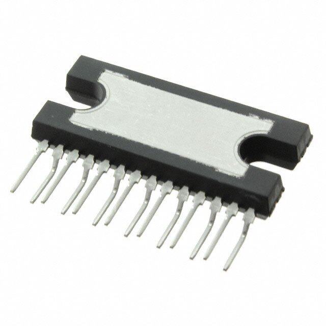
| 供应商器件封装 | 24-TSSOP |
| 其它名称 | 296-13382-1 |
| 包装 | 剪切带 (CT) |
| 安装类型 | 表面贴装 |
| 封装/外壳 | 24-TSSOP(0.173",4.40mm 宽) |
| 工作温度 | -40°C ~ 85°C (TA) |
| 标准包装 | 1 |
| 特性 | 消除爆音,差分输入,短路和热保护,关闭 |
| 电压-电源 | 4.5 V ~ 5.5 V |
| 类型 | D 类 |
| 输出类型 | 2 通道(立体声) |
| 配用 | /product-detail/zh/TPA2000D2EVM/296-10829-ND/381827 |


- 商务部:美国ITC正式对集成电路等产品启动337调查
- 曝三星4nm工艺存在良率问题 高通将骁龙8 Gen1或转产台积电
- 太阳诱电将投资9.5亿元在常州建新厂生产MLCC 预计2023年完工
- 英特尔发布欧洲新工厂建设计划 深化IDM 2.0 战略
- 台积电先进制程称霸业界 有大客户加持明年业绩稳了
- 达到5530亿美元!SIA预计今年全球半导体销售额将创下新高
- 英特尔拟将自动驾驶子公司Mobileye上市 估值或超500亿美元
- 三星加码芯片和SET,合并消费电子和移动部门,撤换高东真等 CEO
- 三星电子宣布重大人事变动 还合并消费电子和移动部门
- 海关总署:前11个月进口集成电路产品价值2.52万亿元 增长14.8%


PDF Datasheet 数据手册内容提取
TPA2000D2 www.ti.com SLOS291F–MARCH2000–REVISEDMARCH2007 2-W FILTERLESS STEREO CLASS-D AUDIO POWER AMPLIFIER FEATURES • Short-CircuitProtection(ShorttoBattery, • ModulationSchemeOptimizedtoOperate Ground,andLoad) WithoutaFilter • -40°Cto85°COperatingTemperatureRange • 2WInto3-W Speakers(THD+N<0.4%) PW OR PWP PACKAGE • <0.08%THD+Nat1W,1kHz,Into4-W Load (TOP VIEW) • ExtremelyEfficientThirdGeneration5-V Class-DTechnology: PGND 1 24 PGND LOUTN 2 23 LOUTP – LowSupplyCurrent(NoFilter) ...8mA GAIN0 3 22 BYPASS – LowSupplyCurrent(Filter) ...15mA PV 4 21 PV DD DD – LowShutdownCurrent...1µA LINN 5 20 LINP AGND 6 19 V – LowNoiseFloor ...56µV DD RMS COSC 7 18 ROSC – MaximumEfficiencyInto3W ,65-70% RINN 8 17 RINP – MaximumEfficiencyInto8W ,75-85% PV 9 16 PV DD DD – 4InternalGainSettings...8-23.5dB SHUTDOWN 10 15 GAIN1 ROUTN 11 14 ROUTP – PSRR...-77dB PGND 12 13 PGND • IntegratedDepopCircuitry DESCRIPTION The TPA2000D2 is the third generation 5-V class-D amplifier from Texas Instruments. Improvements to previous generation devices include: lower supply current, lower noise floor, better efficiency, four different gain settings, smaller packaging, and fewer external components. The most significant advancement with this device is its modulationschemethatallowstheamplifiertooperatewithouttheoutputfilter.Eliminating the output filter saves theuserapproximately30%insystemcostand75%inPCBarea. The TPA2000D2 is a monolithic class-D power IC stereo audio amplifier, using the high switching speed of power MOSFET transistors. These transistors reproduce the analog signal through high-frequency switching of the output stage. The TPA2000D2 is configured as a bridge-tied load (BTL) amplifier capable of delivering greater than 2 W of continuous average power into a 3-W load at less than 1% THD+N from a 5-V power supply in the high fidelity range (20 Hz to 20 kHz). With 1 W being delivered to a 4-W load at 1 kHz, the typical THD+N islessthan0.08%. A BTL configuration eliminates the need for external coupling capacitors on the output. Low supply current of 8 mA makes the device ideal for battery-powered applications. Protection circuitry increases device reliability: thermal,over-current,andunder-voltageshutdown. Efficient class-D modulation enables the TPA2000D2 to operate at full power into 3-W loads at an ambient temperatureof85°C. AVAILABLEOPTIONS(1) PACKAGEDDEVICE T A TSSOP(PW) TSSOP(PWP)(2) –40°Cto85°C TPA2000D2PW TPA2000D2PWP (1) Forthemostcurrentpackageandorderinginformation,seethePackageOptionAddendumattheend ofthisdocument,orseetheTIwebsiteatwww.ti.com. (2) ThePWPpackageisavailabletapedandreeled.Toorderatapedandreeledpart,addthesuffixRto thepartnumber(e.g.,TPA2000D2PWPR). Pleasebeawarethatanimportantnoticeconcerningavailability,standardwarranty,anduseincriticalapplicationsofTexas Instrumentssemiconductorproductsanddisclaimerstheretoappearsattheendofthisdatasheet. PRODUCTIONDATAinformationiscurrentasofpublicationdate. Copyright©2000–2007,TexasInstrumentsIncorporated Products conform to specifications per the terms of the Texas Instruments standard warranty. Production processing does not necessarilyincludetestingofallparameters.
TPA2000D2 www.ti.com SLOS291F–MARCH2000–REVISEDMARCH2007 Thesedeviceshavelimitedbuilt-inESDprotection.Theleadsshouldbeshortedtogetherorthedeviceplacedinconductivefoam duringstorageorhandlingtopreventelectrostaticdamagetotheMOSgates. VDD AGND VDD PVDD Gain RINN + Adjust Gate ROUTN _ Drive _ + PGND _ + PVDD _ Gate Gain ROUTP RINP + Drive Adjust PGND SHUTDOWN OC Start-Up Detect GAIN1 2 Biases Protection GAIN0 Gain and Ramp Logic OC References Generator Detect COSC ROSC Thermal VDD ok BYPASS PVDD Gain LINP + Adjust _ DGraivtee LOUTP _ + PGND _ + PVDD _ Gate LINN Gain + Drive LOUTN Adjust PGND 2 SubmitDocumentationFeedback
TPA2000D2 www.ti.com SLOS291F–MARCH2000–REVISEDMARCH2007 TERMINALFUNCTION TERMINAL I/O DESCRIPTION NAME NO. AGND 6 - Analogground BYPASS 22 I Taptovoltagedividerforinternalmidsupplybiasgeneratorusedforanalogreference. AcapacitorconnectedtothisterminalsetstheoscillationfrequencyinconjunctionwithROSC.For COSC 7 I properoperation,connecta220pFcapacitorfromCOSCtoground. GAIN0 3 I Bit0ofgaincontrol(TTLlogiclevel) GAIN1 15 I Bit1ofgaincontrol(TTLlogiclevel) LINN 5 I Leftchannelnegativedifferentialaudioinput LINP 20 I Leftchannelpositivedifferentialaudioinput LOUTN 2 O Leftchannelnegativeaudiooutput LOUTP 23 O Leftchannelpositiveaudiooutput 1,24 - PowergroundforleftchannelH-bridge PGND 12,13 - PowergroundforrightchannelH-bridge 4,21 - PowersupplyforleftchannelH-bridge PV DD 9,16 - PowersupplyforrightchannelH-bridge RINN 8 I Rightchannelnegativedifferentialaudioinput RINP 17 I Rightchannelpositivedifferentialaudioinput AresistorconnectedtothisterminalsetstheoscillationfrequencyinconjunctionwithCOSC.For ROSC 18 I properoperation,connecta120kW resistorfromROSCtoground. ROUTN 11 O Rightchannelnegativeaudiooutput ROUTP 14 O Rightchannelpositiveoutput PlacestheamplifierinshutdownmodeifaTTLlogiclowisplacedonthisterminal;normaloperationif SHUTDOWN 10 I aTTLlogichighisplacedonthisterminal. V 19 - Analogpowersupply DD ABSOLUTE MAXIMUM RATINGS overoperatingfree-airtemperaturerange(unlessotherwisenoted)(1) UNIT V ,PV Supplyvoltage -0.3Vto6V DD DD V Inputvoltage -0.3VtoV +0.3V I DD Continuoustotalpowerdissipation SeeDissipationRatingTable T Operatingfree-airtemperaturerange -40°Cto85°C A T Operatingjunctiontemperaturerange -40°Cto150°C J T Storagetemperaturerange -65°Cto150°C stg Leadtemperature1,6mm(1/16inch)fromcasefor10seconds 260°C (1) Stressesbeyondthoselistedunderabsolutemaximumratingsmaycausepermanentdamagetothedevice.Thesearestressratings only,andfunctionaloperationofthedeviceattheseoranyotherconditionsbeyondthoseindicatedunderrecommendedoperating conditionsisnotimplied.Exposuretoabsolute-maximum-ratedconditionsforextendedperiodsmayaffectdevicereliability. DISSIPATIONRATINGTABLE T £ 25°C DERATINGFACTOR T =70°C T =85°C PACKAGE A A A POWERRATING ABOVET =25°C POWERRATING POWERRATING A PW 1.04W 8.34mW/°C 0.67W 0.54W PWP 2.7W 21.8mW/°C 1.7W 1.4W SubmitDocumentationFeedback 3
TPA2000D2 www.ti.com SLOS291F–MARCH2000–REVISEDMARCH2007 RECOMMENDED OPERATING CONDITIONS MIN TYP MAX UNIT V ,PV Supplyvoltage 4.5 5.5 V DD DD V High-levelinputvoltage GAIN0,GAIN1,SHUTDOWN 2 V IH V Low-levelinputvoltage GAIN0,GAIN1,SHUTDOWN 0.8 V IL R Oscillatorresistance 120 kW OSC C Oscillatorcapacitance 220 pF OSC f Switchingfrequency 200 300 kHz s T Operatingfree-airtemperature -40 85 °C A ELECTRICAL CHARACTERISTICS T =25°C,V =PV =5V(unlessotherwisenoted) A DD DD PARAMETER TESTCONDITIONS MIN TYP MAX UNIT |V | Outputoffsetvoltage(measureddifferentially) V =0V 25 mV OO I PSRR Powersupplyrejectionratio V =PV =4.5Vto5.5V -77 dB DD DD I High-levelinputcurrent V =PV =5.5V,V =V =PV 1 µA IH DD DD I DD DD I Low-levelinputcurrent V =PV =5.5V,V =0V 1 µA IL DD DD I I Supplycurrent Nofilter(withorwithoutspeakerload) 8 10 mA DD I Supplycurrent Withfilter,L=22µH,C=1µF 15 mA DD I Supplycurrent,shutdownmode 1 15 µA DD(SD) OPERATING CHARACTERISTICS T =25°C,V =PV =5V,R =4W ,Gain=8dB(unlessotherwisenoted) A DD DD L PARAMETER TESTCONDITIONS MIN TYP MAX UNIT P Outputpower THD=0.1%,f=1kHz,R =3W 2 W O L THD+N Totalharmonicdistortionplusnoise P =1W,f=20Hzto20kHz <0.5% O B Maximumoutputpowerbandwidth THD=5% 20 kHz OM k Supplyripplerejectionratio f=1kHz,C =0.4µF -60 dB SVR (BYPASS) SNR Signal-to-noiseratio 87 dBV Integratednoisefloor 20Hzto20kHz,Noinput 56 µV Z Inputimpedance >20 kW I Table1.GainSettings AMPLIFIERGAIN INPUTIMPEDANCE GAIN1 GAIN0 (dB) (kW ) TYP TYP 0 0 8 104 0 1 12 74 1 0 17.5 44 1 1 23.5 24 4 SubmitDocumentationFeedback
TPA2000D2 www.ti.com SLOS291F–MARCH2000–REVISEDMARCH2007 TYPICAL CHARACTERISTICS TableofGraphs FIGURE h Efficiency vsOutputpower 2,3 FFTat1.5Woutputpower vsFrequency 4 vsOutputpower 5-7 THD+N Totalharmonicdistortionplusnoise vsFrequency 8,9 Crosstalk vsFrequency 10 Powersupplyrejectionratio vsFrequency 11 TEST SET-UP FOR GRAPHS The THD+N measurements shown do not use an LC output filter, but use a low pass filter with a cutoff frequency of 20 kHz so the switching frequency does not dominate the measurement. This is done to ensure that the THD+N measured is just the audible THD+N. The THD+N measurements are shown at the highest gain forworstcase. TheLCoutputfilterusedintheefficiencycurves(Figure2andFigure3)isshowninFigure1. L1=L2=22µH(DCR=110mW , Partnumber=SCD0703T-220M-S, Manufacturer=GCI) C1=C2=1µF The ferrite filter used in the efficiency curves (Figure 2 and Figure 3) is shown in Figure 1, where L is a ferrite bead. L1=L2=ferritebead(partnumber=2512067007Y3,manufacturer=Fair-Rite) C1=C2=1nF L1 OUT+ C1 OUT– L2 C2 Figure1.Class-DOutputFilter SubmitDocumentationFeedback 5
TPA2000D2 www.ti.com SLOS291F–MARCH2000–REVISEDMARCH2007 TYPICAL CHARACTERISTICS EFFICIENCY EFFICIENCY vs vs OUTPUTPOWER OUTPUTPOWER 90 80 Ferrite Bead Filter LC Filter Ferrite Bead Filter 80 70 70 60 No Filter LC Filter Notebook Speaker 60 % 50 % cy − 50 y − n Class−AB c 40 e n Effici 40 Efficie 30 Class−AB 30 20 20 10 RVDL D= =8 5W, V Multimedia Speaker 10 RVDL D= =3 5W, V Notebook PC Speaker 0 0 0 0.2 0.4 0.6 0.8 1 1.2 0 0.5 1 1.5 2 PO − Output Power − W PO − Output Power − W Figure2. Figure3. FFTAT1.5WOUTPUTPOWER vs FREQUENCY +0 VDD = 5 V, −20 Gain = 8 dB, f = 1 kHz, B −40 PO = 1.5 W, d Bandwidth = 20 Hz to 22 kHz, V − −60 16386 Frequency Bins r e w −80 o P −100 −120 −140 0 2k 4k 6k 8k 10k 12k 14k 16k 18k 20k 22k 24k f − Frequency − Hz Figure4. 6 SubmitDocumentationFeedback
TPA2000D2 www.ti.com SLOS291F–MARCH2000–REVISEDMARCH2007 TYPICAL CHARACTERISTICS (continued) TOTALHARMONICDISTORTIONPLUSNOISE TOTALHARMONICDISTORTIONPLUSNOISE vs vs OUTPUTPOWER OUTPUTPOWER 10 10 VDD = 5 V VDD = 5 V Gain = 23.5 dB Gain = 23.5 dB − % RL = 3 W − % RL = 4 W n n o o orti orti st 1 st 1 Di Di c c ni 1 kHz ni 1 kHz o o m 20 Hz m ar ar 20 Hz H H al al ot 0.1 ot 0.1 T T − − N N + + D D H 20 kHz H 20 kHz T T 0.01 0.01 10 m 100 m 1 2 3 10 m 100 m 1 2 3 PO − Output Power − W PO − Output Power − W Figure5. Figure6. TOTALHARMONICDISTORTIONPLUSNOISE TOTALHARMONICDISTORTIONPLUSNOISE vs vs OUTPUTPOWER FREQUENCY 10 10 VDD = 5 V VDD = 5 V Distortion − % 1 GRLa i=n 8= W23.5 dB Distortion − % 1 GRLa i=n 4= W23.5 dB monic 1 kHz monic 0.2 W Har 20 Hz Har 0.75 W D+N − Total 0.1 D+N − Total 0.1 1.5 W H 20 kHz H T T 0.01 0.01 10 m 100 m 1 2 20 100 1 k 10 k 20 k PO − Output Power − W f − Frequency − Hz Figure7. Figure8. SubmitDocumentationFeedback 7
TPA2000D2 www.ti.com SLOS291F–MARCH2000–REVISEDMARCH2007 TYPICAL CHARACTERISTICS (continued) TOTALHARMONICDISTORTIONPLUSNOISE vs FREQUENCY 10 VDD = 5 V Gain = 23.5 dB % − RL = 8 W n o orti 1 st Di c 0.1 W ni o m ar 1 W H al 0.1 ot T − N 0.5 W + D H T 0.01 20 100 1 k 20 k f − Frequency − Hz Figure9. CROSSTALK POWERSUPPLYREJECTIONRATIO vs vs FREQUENCY FREQUENCY −30 −30 B d − o −40 ati −40 R n o dB Left to Right cti −50 sstalk − −50 ply Reje −60 o p Cr Su r e Right to Left w −70 o P −60 − R R −80 S P −70 −90 1 10 100 1 k 10 k 100 k 10 100 1 k 10 k 100 k f − Frequency − Hz f − Frequency − Hz Figure10. Figure11. 8 SubmitDocumentationFeedback
TPA2000D2 www.ti.com SLOS291F–MARCH2000–REVISEDMARCH2007 APPLICATION INFORMATION ELIMINATING THE OUTPUT FILTER WITH THE TPA2000D2 ThissectionfocusesonwhytheusercaneliminatetheoutputfilterwiththeTPA2000D2. EFFECT ON AUDIO The class-D amplifier outputs a pulse-width modulated (PWM) square wave, which is the sum of the switching waveform and the amplified input audio signal. The human ear acts as a band-pass filter such that only the frequencies between approximately 20 Hz and 20 kHz are passed. The switching frequency components are muchgreaterthan20kHz,sotheonlysignalheardistheamplifiedinputaudiosignal. TRADITIONAL CLASS-D MODULATION SCHEME The traditional class-D modulation scheme, which is used in the TPA005Dxx family, has a differential output where each output is 180 degrees out of phase and changes from ground to the supply voltage, V . Therefore, DD the differential prefiltered output varies between positive and negative V , where filtered 50% duty cycle yields DD 0 volts across the load. The traditional class-D modulation scheme with voltage and current waveforms is shown in Figure 12. Note that even at an average of 0 volts across the load (50% duty cycle), the current to the load is highcausinghighloss,thuscausingahighsupplycurrent. OUT+ OUT– +5 V Differential Voltage O V Across Load –5 V Current Figure12.TraditionalClass-DModulationScheme'sOutputVoltageandCurrentWaveformsIntoan InductiveLoadWithNoInput TPA2000D2 MODULATION SCHEME The TPA2000D2 uses a modulation scheme that still has each output switching from 0 to the supply voltage. However, OUT+ and OUT- are now in phase with each other with no input. The duty cycle of OUT+ is greater than 50% and OUT- is less than 50% for positive voltages. The duty cycle of OUT+ is less than 50% and OUT- is greater than 50% for negative voltages. The voltage across the load sits at 0 volts throughout most of the switchingperiodgreatlyreducingtheswitchingcurrent,whichreducesanyI2Rlossesintheload. SubmitDocumentationFeedback 9
TPA2000D2 www.ti.com SLOS291F–MARCH2000–REVISEDMARCH2007 APPLICATION INFORMATION (continued) OUT+ OUT– Output = 0 V Differential +5 V Voltage 0 V Across –5 V Load Current OUT+ OUT– Output > 0 V Differential +5 V Voltage 0 V Across –5 V Load Current Figure13.TheTPA2000D2OutputVoltageandCurrentWaveformsIntoanInductiveLoad EFFICIENCY: WHY YOU MUST USE A FILTER WITH THE TRADITIONAL CLASS-D MODULATION SCHEME The main reason that the traditional class-D amplifier needs an output filter is that the switching waveform results in maximum current flow. This causes more loss in the load, which causes lower efficiency. The ripple current is large for the traditional modulation scheme because the ripple current is proportional to voltage multiplied by the time at that voltage. The differential voltage swing is 2 × V and the time at each voltage is DD half the period for the traditional modulation scheme. An ideal LC filter is needed to store the ripple current from each half cycle for the next half cycle, while any resistance causes power dissipation. The speaker is both resistiveandreactive,whereasanLCfilterisalmostpurelyreactive. The TPA2000D2 modulation scheme has very little loss in the load without a filter because the pulses are very short and the change in voltage is V instead of 2 × V . As the output power increases, the pulses widen DD DD making the ripple current larger. Ripple current could be filtered with an LC filter for increased efficiency, but for mostapplicationsthefilterisnotneeded. An LC filter with a cutoff frequency less than the class-D switching frequency allows the switching current to flow through the filter instead of the load. The filter has less resistance than the speaker, which results in less power dissipatedandincreasedefficiency. EFFECTS OF APPLYING A SQUARE WAVE INTO A SPEAKER Audiospecialistshavesaidforyearsnottoapplyasquarewavetospeakers.If the amplitude of the waveform is high enough and the frequency of the square wave is within the bandwidth of the speaker, the square wave could cause the voice coil to jump out of the air gap and/or scar the voice coil. A 250-kHz switching frequency, however, is not significant because the speaker cone movement is proportional to 1/f2 for frequencies beyond the audio band. Therefore, the amount of cone movement at the switching frequency is very small. However, 10 SubmitDocumentationFeedback
TPA2000D2 www.ti.com SLOS291F–MARCH2000–REVISEDMARCH2007 APPLICATION INFORMATION (continued) damage could occur to the speaker if the voice coil is not designed to handle the additional power. To size the speaker for added power, the ripple current dissipated in the load needs to be calculated by subtracting the theoretical supplied power, P , from the actual supply power, P , at maximum output power, SUP THEORETICAL SUP P . The switching power dissipated in the speaker is the inverse of the measured efficiency,h , minus OUT MEASURED thetheoreticalefficiency,h . THEORETICAL PSPKR = PSUP – PSUP THEORETICAL (at max output power) (1) PSPKR = PSUP / POUT – PSUP THEORETICAL / POUT (at max output power) (2) P = 1/h – 1/h (at max output power) SPKR MEASURED THEORETICAL (3) The maximum efficiency of the TPA2000D2 with an 8-W load is 85%. Using Equation 3 with the efficiency at maximum power from Figure 2 (78%), we see that there is an additional 106 mW dissipated in the speaker. The added power dissipated in the speaker is not an issue as long as it is taken into account when choosing the speaker. WHEN TO USE AN OUTPUT FILTER Design the TPA2000D2 without the filter if the traces from amplifier to speaker are short. The TPA2000D2 passed FCC and CE radiated emissions with no shielding with speaker wires 8 inches (20,32 cm) long or less. Notebook PCs and powered speakers where the speaker is in the same enclosure as the amplifier are good applicationsforclass-Dwithoutafilter. Aferritebeadfiltercanoftenbeusedif the design is failing radiated emissions without a filter, and the frequency sensitive circuit is greater than 1 MHz. This is good for circuits that just have to pass FCC and CE because FCC and CE only test radiated emissions greater than 30 MHz. If choosing a ferrite bead, choose one with high impedanceathighfrequencies,butverylowimpedanceatlowfrequencies. Use an output filter if there are low frequency (< 1 MHz) EMI sensitive circuits and/or there are long leads from amplifiertospeaker. GAIN SETTING VIA GAIN0 AND GAIN1 INPUTS ThegainoftheTPA2000D2issetbytwoinputterminals,GAIN0andGAIN1. The gains listed in Table 2 are realized by changing the taps on the input resistors inside the amplifier. This causes the input impedance, Z, to be dependent on the gain setting. The actual gain settings are controlled by I ratios of resistors, so the actual gain distribution from part-to-part is quite good. However, the input impedance mayshiftby30%duetoshiftsintheactualresistanceoftheinputresistors. For design purposes, the input network (discussed in the next section) should be designed assuming an input impedance of 20 kW , which is the absolute minimum input impedance of the TPA2000D2. At the lower gain settings,theinputimpedancecouldincreasetoashighas115kW . Table2.GainSettings AMPLIFIERGAIN INPUTIMPEDANCE GAIN1 GAIN0 (dB) (kW ) TYP TYP 0 0 8 104 0 1 12 74 1 0 17.5 44 1 1 23.5 24 SubmitDocumentationFeedback 11
TPA2000D2 www.ti.com SLOS291F–MARCH2000–REVISEDMARCH2007 INPUT RESISTANCE Each gain setting is achieved by varying the input resistance of the amplifier, which can range from its smallest valuetoover6timesthatvalue. ZF Input CI IN ZI Signal The-3dBfrequencycanbecalculatedusingEquation4: f(cid:1)3dB(cid:2)2(cid:1)C1 Z I I (4) INPUT CAPACITOR, C I In the typical application an input capacitor, C, is required to allow the amplifier to bias the input signal to the I proper dc level for optimum operation. In this case, C and the input impedance of the amplifier, Z, form a I I high-passfilterwiththecornerfrequencydeterminedinEquation5. −3 dB f (cid:1) 1 c(highpass) 2(cid:1)Z C I I fc (5) The value of C is important, as it directly affects the bass (low frequency) performance of the circuit. Consider I the example where Z is 20 kW and the specification calls for a flat bass response down to 80 Hz. Equation 5 is I reconfiguredasEquation6. C (cid:1) 1 I 2(cid:1)Z f I c (6) In this example, C is 0.1 µF, so one would likely choose a value in the range of 0.1 µF to 1 µF. If the gain is I known and is constant, use Z from Table 1 to calculate C. A further consideration for this capacitor is the I I leakage path from the input source through the input network (C) and the feedback network to the load. This I leakage current creates a dc offset voltage at the input to the amplifier that reduces useful headroom, especially in high gain applications. For this reason a low-leakage tantalum or ceramic capacitor is the best choice. When polarized capacitors are used, the positive side of the capacitor should face the amplifier input in most applications as the dc level there is held at V /2, which is likely higher than the source dc level. Note that it is DD importanttoconfirmthecapacitorpolarityintheapplication. C should be 10 times smaller than the bypass capacitor to reduce clicking and popping noise from power on/off I and entering and leaving shutdown. After sizing CI for a given cutoff frequency, size the bypass capacitor up to 10timesthatoftheinputcapacitor. C ≤ C / 10 I BYP (7) 12 SubmitDocumentationFeedback
TPA2000D2 www.ti.com SLOS291F–MARCH2000–REVISEDMARCH2007 SWITCHING FREQUENCY TheswitchingfrequencyisdeterminedusingthevaluesofthecomponentsconnectedtoR (pin 18) and C OSC OSC (pin7)andiscalculatedwiththefollowingequation: f (cid:1) 6.6 s R C OSC OSC (8) The switching frequency was chosen to be centered on 250 kHz. This frequency is the optimum audio fidelity of oversampling and of maximizing efficiency by minimizing the switching losses of the amplifier. The recommended values are a resistance of 120 kW and a capacitance of 220 pF. Using these component values, the amplifier operates properly by using 5% tolerance resistors and 10% tolerance capacitors. The tolerance of the components can be changed, as long as the switching frequency remains between 200 kHz and 300 kHz. Withinthisrange,theinternalcircuitryofthedeviceprovidesstableoperation. POWER SUPPLY DECOUPLING, C S The TPA2000D2 is a high-performance CMOS audio amplifier that requires adequate power supply decoupling to ensure the output total harmonic distortion (THD) is as low as possible. Power supply decoupling also prevents oscillations for long lead lengths between the amplifier and the speaker. The optimum decoupling is achievedbyusingtwocapacitorsofdifferenttypesthat target different types of noise on the power supply leads. For higher frequency transients, spikes, or digital hash on the line, a good low equivalent-series-resistance (ESR) ceramic capacitor, typically 0.1 µF placed as close as possible to the device V lead works best. For DD filtering lower-frequency noise signals, a larger aluminum electrolytic capacitor of 10 µF or greater placed near theaudiopoweramplifierisrecommended. MIDRAIL BYPASS CAPACITOR, C BYP The midrail bypass capacitor, C , is the most critical capacitor and serves several important functions. During BYP start-up or recovery from shutdown mode, C determines the rate at which the amplifier starts up. The second BYP function is to reduce noise produced by the power supply caused by coupling into the output drive signal. This noise is from the midrail generation circuit internal to the amplifier, which appears as degraded PSRR and THD+N. Bypass capacitor, C , values of 0.47 µF to 1 µF ceramic or tantalum low-ESR capacitors are recommended BYP forthebestTHDandnoiseperformance. Increasing the bypass capacitor reduces clicking and popping noise from power on/off and entering and leaving shutdown.Tohaveminimalpop,C shouldbe10timeslargerthanC. BYP I C ≥ 10 × C BYP I (9) DIFFERENTIAL INPUT The differential input stage of the amplifier cancels any noise that appears on both input lines of a channel. To use the TPA2000D2 EVM with a differential source, connect the positive lead of the audio source to the RINP (LINP) input and the negative lead from the audio source to the RINN (LINN) input. To use the TPA2000D2 with a single-ended source, ac ground the RINN and LINN inputs through a capacitor and apply the audio single to the RINP and LINP inputs. In a single-ended input application, the RINN and LINN inputs should be ac-groundedattheaudiosourceinsteadofatthedeviceinputsforbestnoiseperformance. SHUTDOWN MODES The TPA2000D2 employs a shutdown mode of operation designed to reduce supply current, I , to the absolute DD minimum level during periods of nonuse for battery-power conservation. The SHUTDOWN input terminal should be held high during normal operation when the amplifier is in use. Pulling SHUTDOWN low causes the outputs to mute and the amplifier to enter a low-current state, I = 1 µA. SHUTDOWN should never be left DD(SD) unconnected,becauseamplifieroperationwouldbeunpredictable. SubmitDocumentationFeedback 13
TPA2000D2 www.ti.com SLOS291F–MARCH2000–REVISEDMARCH2007 USING LOW-ESR CAPACITORS Low-ESR capacitors are recommended throughout this application section. A real (as opposed to ideal) capacitor can be modeled simply as a resistor in series with an ideal capacitor. The voltage drop across this resistor minimizes the beneficial effects of the capacitor in the circuit. The lower the equivalent value of this resistancethemoretherealcapacitorbehaveslikeanidealcapacitor. EVALUATION CIRCUIT C1 0.1 m F LEFT AUDIO INPUT+ LEFT AUDIO OUTPUT– VDD TPA2000D2 PGND PGND LOUTN LOUTP LEFT AUDIO OUTPUT+ C5 1 m F GAIN SELECT GAIN0 BYPASS C2 C17 C6 10 m F 0.1 m F LPVDD LPVDD LEFT AUDIO INPUT– 0.1 m F LINN LINP20 0.1 mCF21 VDD AGND VDD VDD C3 C7 C20 R1 0.1 m F COSC ROSC 220 pF 0.1 m F 120k RIGHT AUDIO INPUT+ RINN RINP C8 RPVDD RPVDD 10 m F 10 C19 TO SYSTEM CONTROL SHUTDOWN GAIN1 GAIN SELECT 0.1 m F C18 ROUTN ROUTP RIGHT AUDIO OUTPUT + 0.1 m F PGND PGND VDD RIGHT AUDIO OUTPUT – C4 RIGHT AUDIO INPUT– 0.1 m F Table3.TPA2000D2ApplicationBillofMaterials REFERENCE DESCRIPTION SIZE QUANTITY MANUFACTURER PARTNUMBER C1-4,C17-21 Capacitor,ceramicchip,0.1µF,±10%,X7R,50V 0805 9 Kemet C0805C104K5RAC C5 Capacitor,ceramic,1.0µF,80%/-20%,Y5V,16V 0805 1 Murata GRM40-Y5V105Z16 C6,C8 Capacitor,ceramic,10µF,80%/-20%,Y5V,16V 1210 2 Murata GRM235-Y5V106Z16 C7 Capacitor,ceramic,220pF,±10%,XICON,50V 0805 2 Mouser 140-CC501B221K R1 Resistor,chip,120kW ,1/10W,5%,XICON 0805 1 Mouser 260-120K IC,TPA2000D2,audiopoweramplifier,2-W, 24pin U1 1 TI TPA2000D2PWP 2-channel,class-D TSSOP 14 SubmitDocumentationFeedback
PACKAGE OPTION ADDENDUM www.ti.com 6-Feb-2020 PACKAGING INFORMATION Orderable Device Status Package Type Package Pins Package Eco Plan Lead/Ball Finish MSL Peak Temp Op Temp (°C) Device Marking Samples (1) Drawing Qty (2) (6) (3) (4/5) TPA2000D2PW ACTIVE TSSOP PW 24 60 Green (RoHS NIPDAU Level-2-260C-1 YEAR -40 to 85 TPA2000D2 & no Sb/Br) TPA2000D2PWP ACTIVE HTSSOP PWP 24 60 Green (RoHS NIPDAU Level-2-260C-1 YEAR -40 to 85 TPA2000D2 & no Sb/Br) TPA2000D2PWPG4 ACTIVE HTSSOP PWP 24 60 Green (RoHS NIPDAU Level-2-260C-1 YEAR -40 to 85 TPA2000D2 & no Sb/Br) TPA2000D2PWPR ACTIVE HTSSOP PWP 24 2000 Green (RoHS NIPDAU Level-2-260C-1 YEAR -40 to 85 TPA2000D2 & no Sb/Br) TPA2000D2PWR ACTIVE TSSOP PW 24 2000 Green (RoHS NIPDAU Level-2-260C-1 YEAR -40 to 85 TPA2000D2 & no Sb/Br) TPA2000D2PWRG4 ACTIVE TSSOP PW 24 2000 Green (RoHS NIPDAU Level-2-260C-1 YEAR -40 to 85 TPA2000D2 & no Sb/Br) (1) The marketing status values are defined as follows: ACTIVE: Product device recommended for new designs. LIFEBUY: TI has announced that the device will be discontinued, and a lifetime-buy period is in effect. NRND: Not recommended for new designs. Device is in production to support existing customers, but TI does not recommend using this part in a new design. PREVIEW: Device has been announced but is not in production. Samples may or may not be available. OBSOLETE: TI has discontinued the production of the device. (2) RoHS: TI defines "RoHS" to mean semiconductor products that are compliant with the current EU RoHS requirements for all 10 RoHS substances, including the requirement that RoHS substance do not exceed 0.1% by weight in homogeneous materials. Where designed to be soldered at high temperatures, "RoHS" products are suitable for use in specified lead-free processes. TI may reference these types of products as "Pb-Free". RoHS Exempt: TI defines "RoHS Exempt" to mean products that contain lead but are compliant with EU RoHS pursuant to a specific EU RoHS exemption. Green: TI defines "Green" to mean the content of Chlorine (Cl) and Bromine (Br) based flame retardants meet JS709B low halogen requirements of <=1000ppm threshold. Antimony trioxide based flame retardants must also meet the <=1000ppm threshold requirement. (3) MSL, Peak Temp. - The Moisture Sensitivity Level rating according to the JEDEC industry standard classifications, and peak solder temperature. (4) There may be additional marking, which relates to the logo, the lot trace code information, or the environmental category on the device. (5) Multiple Device Markings will be inside parentheses. Only one Device Marking contained in parentheses and separated by a "~" will appear on a device. If a line is indented then it is a continuation of the previous line and the two combined represent the entire Device Marking for that device. Addendum-Page 1
PACKAGE OPTION ADDENDUM www.ti.com 6-Feb-2020 (6) Lead/Ball Finish - Orderable Devices may have multiple material finish options. Finish options are separated by a vertical ruled line. Lead/Ball Finish values may wrap to two lines if the finish value exceeds the maximum column width. Important Information and Disclaimer:The information provided on this page represents TI's knowledge and belief as of the date that it is provided. TI bases its knowledge and belief on information provided by third parties, and makes no representation or warranty as to the accuracy of such information. Efforts are underway to better integrate information from third parties. TI has taken and continues to take reasonable steps to provide representative and accurate information but may not have conducted destructive testing or chemical analysis on incoming materials and chemicals. TI and TI suppliers consider certain information to be proprietary, and thus CAS numbers and other limited information may not be available for release. In no event shall TI's liability arising out of such information exceed the total purchase price of the TI part(s) at issue in this document sold by TI to Customer on an annual basis. Addendum-Page 2
PACKAGE MATERIALS INFORMATION www.ti.com 26-Feb-2019 TAPE AND REEL INFORMATION *Alldimensionsarenominal Device Package Package Pins SPQ Reel Reel A0 B0 K0 P1 W Pin1 Type Drawing Diameter Width (mm) (mm) (mm) (mm) (mm) Quadrant (mm) W1(mm) TPA2000D2PWPR HTSSOP PWP 24 2000 330.0 16.4 6.95 8.3 1.6 8.0 16.0 Q1 TPA2000D2PWR TSSOP PW 24 2000 330.0 16.4 6.95 8.3 1.6 8.0 16.0 Q1 PackMaterials-Page1
PACKAGE MATERIALS INFORMATION www.ti.com 26-Feb-2019 *Alldimensionsarenominal Device PackageType PackageDrawing Pins SPQ Length(mm) Width(mm) Height(mm) TPA2000D2PWPR HTSSOP PWP 24 2000 367.0 367.0 38.0 TPA2000D2PWR TSSOP PW 24 2000 350.0 350.0 43.0 PackMaterials-Page2
PACKAGE OUTLINE PW0024A TSSOP - 1.2 mm max height SCALE 2.000 SMALL OUTLINE PACKAGE SEATING PLANE C 6.6 TYP 6.2 A 0.1 C PIN 1 INDEX AREA 22X 0.65 24 1 2X 7.9 7.15 7.7 NOTE 3 12 13 0.30 24X B 4.5 0.19 1.2 MAX 4.3 0.1 C A B NOTE 4 0.25 GAGE PLANE 0.15 0.05 (0.15) TYP SEE DETAIL A 0.75 0 -8 0.50 DETA 20AIL A TYPICAL 4220208/A 02/2017 NOTES: 1. All linear dimensions are in millimeters. Any dimensions in parenthesis are for reference only. Dimensioning and tolerancing per ASME Y14.5M. 2. This drawing is subject to change without notice. 3. This dimension does not include mold flash, protrusions, or gate burrs. Mold flash, protrusions, or gate burrs shall not exceed 0.15 mm per side. 4. This dimension does not include interlead flash. Interlead flash shall not exceed 0.25 mm per side. 5. Reference JEDEC registration MO-153. www.ti.com
EXAMPLE BOARD LAYOUT PW0024A TSSOP - 1.2 mm max height SMALL OUTLINE PACKAGE 24X (1.5) SYMM (R0.05) TYP 1 24X (0.45) 24 22X (0.65) SYMM 12 13 (5.8) LAND PATTERN EXAMPLE EXPOSED METAL SHOWN SCALE: 10X SOLDER MASK METAL METAL UNDER SOLDER MASK OPENING SOLDER MASK OPENING EXPOSED METAL EXPOSED METAL 0.05 MAX 0.05 MIN ALL AROUND ALL AROUND NON-SOLDER MASK SOLDER MASK DEFINED DEFINED (PREFERRED) SOLDE15.000R MASK DETAILS 4220208/A 02/2017 NOTES: (continued) 6. Publication IPC-7351 may have alternate designs. 7. Solder mask tolerances between and around signal pads can vary based on board fabrication site. www.ti.com
EXAMPLE STENCIL DESIGN PW0024A TSSOP - 1.2 mm max height SMALL OUTLINE PACKAGE 24X (1.5) SYMM (R0.05) TYP 1 24X (0.45) 24 22X (0.65) SYMM 12 13 (5.8) SOLDER PASTE EXAMPLE BASED ON 0.125 mm THICK STENCIL SCALE: 10X 4220208/A 02/2017 NOTES: (continued) 8. Laser cutting apertures with trapezoidal walls and rounded corners may offer better paste release. IPC-7525 may have alternate design recommendations. 9. Board assembly site may have different recommendations for stencil design. www.ti.com
GENERIC PACKAGE VIEW PWP 24 PowerPADTM TSSOP - 1.2 mm max height 4.4 x 7.6, 0.65 mm pitch PLASTIC SMALL OUTLINE This image is a representation of the package family, actual package may vary. Refer to the product data sheet for package details. 4224742/B www.ti.com
PACKAGE OUTLINE PWP0024B PowerPAD T M TSSOP - 1.2 mm max height SCALE 2.200 PLASTIC SMALL OUTLINE 6.6 TYP SEATING PLANE C 6.2 PIN 1 ID A AREA 0.1 C 22X 0.65 24 1 7.9 2X 7.7 7.15 NOTE 3 12 13 0.30 4.5 24X B 0.19 4.3 0.1 C A B (0.15) TYP SEE DETAIL A 4X (0.2) MAX 2X (0.95) MAX NOTE 5 NOTE 5 EXPOSED THERMAL PAD 0.25 5.16 GAGE PLANE 1.2 MAX 4.12 0.15 0 - 8 0.05 0.75 0.50 DETAIL A (1) TYPICAL 2.40 1.65 4222709/A 02/2016 PowerPAD is a trademark of Texas Instruments. NOTES: 1. All linear dimensions are in millimeters. Any dimensions in parenthesis are for reference only. Dimensioning and tolerancing per ASME Y14.5M. 2. This drawing is subject to change without notice. 3. This dimension does not include mold flash, protrusions, or gate burrs. Mold flash, protrusions, or gate burrs shall not exceed 0.15 mm per side. 4. Reference JEDEC registration MO-153. 5. Features may not be present and may vary. www.ti.com
EXAMPLE BOARD LAYOUT PWP0024B PowerPAD T M TSSOP - 1.2 mm max height PLASTIC SMALL OUTLINE (3.4) NOTE 9 SOLDER MASK DEFINED PAD (2.4) 24X (1.5) SYMM SEE DETAILS 1 24 24X (0.45) (R0.05) TYP (1.1) (7.8) SYMM TYP NOTE 9 (5.16) 22X (0.65) ( 0.2) TYP VIA 12 13 METAL COVERED (1) TYP BY SOLDER MASK (5.8) LAND PATTERN EXAMPLE SCALE:10X SOOPLEDNEINRG MASK METAL SMOELTDAELR U MNDAESRK SOOPLEDNEINRG MASK 0.05 MIN 0.05 MAX ALL AROUND ALL AROUND NON SOLDER MASK SOLDER MASK DEFINED DEFINED SOLDER MASK DETAILS PADS 1-24 4222709/A 02/2016 NOTES: (continued) 6. Publication IPC-7351 may have alternate designs. 7. Solder mask tolerances between and around signal pads can vary based on board fabrication site. 8. This package is designed to be soldered to a thermal pad on the board. For more information, see Texas Instruments literature numbers SLMA002 (www.ti.com/lit/slma002) and SLMA004 (www.ti.com/lit/slma004). 9. Size of metal pad may vary due to creepage requirement. www.ti.com
EXAMPLE STENCIL DESIGN PWP0024B PowerPAD T M TSSOP - 1.2 mm max height PLASTIC SMALL OUTLINE (2.4) BASED ON 0.125 THICK 24X (1.5) STENCIL (R0.05) TYP 1 24 24X (0.45) (5.16) SYMM BASED ON 0.125 THICK STENCIL 22X (0.65) 12 13 SYMM METAL COVERED BY SOLDER MASK SEE TABLE FOR DIFFERENT OPENINGS (5.8) FOR OTHER STENCIL THICKNESSES SOLDER PASTE EXAMPLE EXPOSED PAD 100% PRINTED SOLDER COVERAGE BY AREA SCALE:10X STENCIL SOLDER STENCIL THICKNESS OPENING 0.1 2.68 X 5.77 0.125 2.4 X 5.16 (SHOWN) 0.15 2.19 X 4.71 0.175 2.03 X 4.36 4222709/A 02/2016 NOTES: (continued) 10. Laser cutting apertures with trapezoidal walls and rounded corners may offer better paste release. IPC-7525 may have alternate design recommendations. 11. Board assembly site may have different recommendations for stencil design. www.ti.com
IMPORTANTNOTICEANDDISCLAIMER TI PROVIDES TECHNICAL AND RELIABILITY DATA (INCLUDING DATASHEETS), DESIGN RESOURCES (INCLUDING REFERENCE DESIGNS), APPLICATION OR OTHER DESIGN ADVICE, WEB TOOLS, SAFETY INFORMATION, AND OTHER RESOURCES “AS IS” AND WITH ALL FAULTS, AND DISCLAIMS ALL WARRANTIES, EXPRESS AND IMPLIED, INCLUDING WITHOUT LIMITATION ANY IMPLIED WARRANTIES OF MERCHANTABILITY, FITNESS FOR A PARTICULAR PURPOSE OR NON-INFRINGEMENT OF THIRD PARTY INTELLECTUAL PROPERTY RIGHTS. These resources are intended for skilled developers designing with TI products. You are solely responsible for (1) selecting the appropriate TI products for your application, (2) designing, validating and testing your application, and (3) ensuring your application meets applicable standards, and any other safety, security, or other requirements. These resources are subject to change without notice. TI grants you permission to use these resources only for development of an application that uses the TI products described in the resource. Other reproduction and display of these resources is prohibited. No license is granted to any other TI intellectual property right or to any third party intellectual property right. TI disclaims responsibility for, and you will fully indemnify TI and its representatives against, any claims, damages, costs, losses, and liabilities arising out of your use of these resources. TI’s products are provided subject to TI’s Terms of Sale (www.ti.com/legal/termsofsale.html) or other applicable terms available either on ti.com or provided in conjunction with such TI products. TI’s provision of these resources does not expand or otherwise alter TI’s applicable warranties or warranty disclaimers for TI products. Mailing Address: Texas Instruments, Post Office Box 655303, Dallas, Texas 75265 Copyright © 2020, Texas Instruments Incorporated