 Datasheet下载
- 型号: TN1205H-6T
- 制造商: STMicroelectronics
- 库位|库存: xxxx|xxxx
- 要求:
| 数量阶梯 | 香港交货 | 国内含税 |
| +xxxx | $xxxx | ¥xxxx |
查看当月历史价格
查看今年历史价格
TN1205H-6T产品简介:
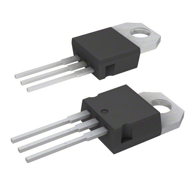
ICGOO电子元器件商城为您提供TN1205H-6T由STMicroelectronics设计生产,在icgoo商城现货销售,并且可以通过原厂、代理商等渠道进行代购。 TN1205H-6T价格参考。STMicroelectronicsTN1205H-6T封装/规格:晶闸管 - SCR, SCR 600V 12A Standard Recovery Through Hole TO-220AB。您可以下载TN1205H-6T参考资料、Datasheet数据手册功能说明书,资料中有TN1205H-6T 详细功能的应用电路图电压和使用方法及教程。
STMicroelectronics(意法半导体)生产的TN1205H-6T是一款晶闸管(SCR,Silicon Controlled Rectifier),属于功率半导体器件。其主要应用场景包括以下几类:

1. 电机控制与启动
   TN1205H-6T可用于电机的软启动和速度控制。通过调节SCR的导通角,可以实现对电机电压的精确控制,从而降低启动电流冲击并优化运行效率。适用于工业设备中的交流电机驱动。

2. 电力调节与调光
   该型号适合用于灯光调光系统(如白炽灯或卤素灯调光)。通过相位控制技术,SCR能够调整输出到负载的功率,从而实现亮度调节。此外,它也适用于加热元件的功率控制,例如电炉、烤箱等家用或工业设备。

3. 开关电源与逆变器
   在开关电源和逆变器中,TN1205H-6T可以用作高压开关元件,帮助实现直流到交流的转换或稳压功能。这种应用常见于不间断电源(UPS)、太阳能逆变器和其他需要高效能量转换的场合。

4. 过压保护与电路切换
   SCR具有快速响应的特点,因此可作为过压保护装置的核心组件。当检测到异常高电压时,TN1205H-6T会迅速触发以分流多余电流,保护下游敏感设备。同时,在某些配电系统中,它可以用于自动切换备用电源或隔离故障部分。

5. 焊接设备
   在电阻焊机或其他类型焊接设备中,TN1205H-6T能够提供精确的电流控制,确保焊接过程稳定且一致。这有助于提高焊接质量并延长设备寿命。

总结来说,TN1205H-6T凭借其高耐压能力(600V)、大电流承载能力和可靠性能,广泛应用于需要功率调节、开关控制及保护功能的各种电气和电子系统中。选择具体应用场景时,需结合实际需求考虑散热设计、驱动电路匹配等因素。
| 参数 | 数值 |
| 产品目录 | |
| 描述 | SCR 12A 600V TO-220SCR High Temp 12A SCR 600V 2 to 5 mA IGT |
| 产品分类 | SCR - 单个分离式半导体 |
| GateTriggerCurrent-Igt | 5 mA |
| GateTriggerVoltage-Vgt | 1.3 V |
| 品牌 | STMicroelectronics |
| 产品手册 | |
| 产品图片 |
|
| rohs | 符合RoHS无铅 / 符合限制有害物质指令(RoHS)规范要求 |
| 产品系列 | 晶体闸流管,SCR,STMicroelectronics TN1205H-6T- |
| 数据手册 | |
| 产品型号 | TN1205H-6T |
| SCR类型 | 标准恢复型 |
| 产品培训模块 | http://www.digikey.cn/PTM/IndividualPTM.page?site=cn&lang=zhs&ptm=26297http://www.digikey.cn/PTM/IndividualPTM.page?site=cn&lang=zhs&ptm=26298 |
| 产品种类 | SCR |
| 供应商器件封装 | TO-220AB |
| 保持电流Ih最大值 | 20 mA |
| 其它名称 | 497-11369-5 |
| 其它有关文件 | http://www.st.com/web/catalog/sense_power/FM144/CL1220/SC111/PF251674?referrer=70071840 |
| 包装 | 管件 |
| 商标 | STMicroelectronics |
| 安装类型 | 通孔 |
| 安装风格 | Through Hole |
| 封装 | Tube |
| 封装/外壳 | TO-220-3 |
| 封装/箱体 | TO-220-3 |
| 工作温度 | -40°C ~ 150°C |
| 工厂包装数量 | 50 |
| 开启状态RMS电流-ItRMS | 12 A |
| 最大工作温度 | + 150 C |
| 栅极触发电压-Vgt | 1.3 V |
| 栅极触发电流-Igt | 5 mA |
| 标准包装 | 50 |
| 电压-断态 | 600V |
| 电压-栅极触发(Vgt)(最大值) | 1.3V |
| 电压-通态(Vtm)(最大值) | 1.6V |
| 电流-不重复浪涌50、60Hz(Itsm) | 120A,126A |
| 电流-保持(Ih)(最大值) | 20mA |
| 电流-断态(最大值) | 5µA |
| 电流-栅极触发(Igt)(最大值) | 5mA |
| 电流-通态(It(AV))(最大值) | 7.6A |
| 电流-通态(It(RMS))(最大值) | 12A |
| 系列 | TN1205H |
| 额定重复关闭状态电压VDRM | 600 V |


- 商务部:美国ITC正式对集成电路等产品启动337调查
- 曝三星4nm工艺存在良率问题 高通将骁龙8 Gen1或转产台积电
- 太阳诱电将投资9.5亿元在常州建新厂生产MLCC 预计2023年完工
- 英特尔发布欧洲新工厂建设计划 深化IDM 2.0 战略
- 台积电先进制程称霸业界 有大客户加持明年业绩稳了
- 达到5530亿美元!SIA预计今年全球半导体销售额将创下新高
- 英特尔拟将自动驾驶子公司Mobileye上市 估值或超500亿美元
- 三星加码芯片和SET,合并消费电子和移动部门,撤换高东真等 CEO
- 三星电子宣布重大人事变动 还合并消费电子和移动部门
- 海关总署:前11个月进口集成电路产品价值2.52万亿元 增长14.8%


PDF Datasheet 数据手册内容提取
TN1205H High temperature 12 A SCRs − Datasheet production data Features A ■ High junction temperature: T = 150 °C j ■ Medium current SCRs G ■ High noise immunity up to 150 °C K ■ RoHS (2002/95/EC) compliant A A ■ 600 V V , V DRM RRM Application K A K G A G ■ General purpose AC line load switching D2PAK ■ Motor control circuits (TN1205H-6G) TO-220AB (TN1205H-6T) ■ Small home appliances ■ Lighting ■ Inrush current limiting circuits Table 1. Device summary ■ Over-voltage crowbar protection Order code Package VDRM, I V GT RRM Description TN1205H-6T TO-220AB 600 V 2 to 5 mA TN1205H-6G D2PAK Available in standard gate triggering levels, the TN1205H SCR series has very high switching capability up to junction temperature of 150 °C. These products fit all modes of control found in applications such as overvoltage crowbar protection, motor control circuits in power tools and kitchen aids, inrush current limiting circuits, capacitive discharge ignition and voltage regulation circuits. These products are particulary adapted for use in areas where the ambient temperature is high or the ventilation low, or where an increase of power density is required. Through-hole or surface-mount packages provide performance in a limited space area. April 2012 Doc ID 018497 Rev 4 1/10 This is information on a product in full production. www.st.com 10
Characteristics TN1205H 1 Characteristics Table 2. A bsolute ratings (limiting values) Symbol Parameter Value Unit IT(RMS) On-state rms current (180° conduction angle) TO220-AB, 12 A T = 136 °C I Average on-state current (180° conduction angle) D2PAK c 7.6 A T(AV) t = 8.3 ms 126 p I Non repetitive surge peak on-state current T = 25 °C A TSM j t = 10 ms 120 p I2t I2t Value for fusing t = 10 ms 72 A2S p V , V , V DSM Non repetitive surge peak off-state voltage t = 10 ms DRM RRM V V p +100 RSM Critical rate of rise of on-state current I = 2 x I , dI/dt G GT F = 60 Hz T = 150 °C 100 A/µs t ≤ 100 ns j r I Peak gate current t = 20 µs T = 150 °C 4 A GM p j P Average gate power dissipation T = 150 °C 1 W G(AV) j V Maximum peak reverse gate voltage 5 V RGM T Storage junction temperature range stg - 40 to + 150 °C T Operating junction temperature range j T Maximum lead temperature for soldering during 10 s. 260 °C L Table 3. E lectrical characteristics (T = 25 °C, unless otherwise specified) j Symbol Test conditions Value Unit MIN. 2 I V = 12 V, R = 33 Ω mA GT D L MAX. 5 V V = V , R = 3.3 kΩ MAX. 1.3 V GT D DRM L V V = V , R = 3.3 kΩ MIN. 0.2 V GD D DRM L I I = 500 mA gate open MAX. 20 mA H T I I = 1.2 I MAX. 40 mA L G GT T = 125 °C 200 j dV/dt V = 67% V gate open MIN. V/µs D DRM T = 150 °C 100 j t I = 40 A, V = 500 V, I = 100 mA, dI /dt = 5 A/µs typ. 1.9 µs gt TM D G G V = 335 V, Tj =125 °C, I = 20 A, V = 25 V, (dI /dt) = 30 A/µs, t DM TM R T Max typ. 65 µs q dV /dt = 50 V/µs, R = 100 Ω D GK 2/10 Doc ID 018497 Rev 4
TN1205H Characteristics Table 4. S tatic characteristics Symbol Test conditions Value Unit V I = 24 A, t = 380 µs T = 25 °C 1.6 V T TM p j V Threshold voltage T = 150 °C 0.8 V TD j R Dynamic resistance T = 150 °C 30 mΩ d j MAX. T = 25 °C 5 µA j I DRM V = V T = 125 °C 1 IRRM DRM RRM j mA T = 150 °C 3 j Table 5. T hermal resistance Symbol Parameter Value Max. Unit R Junction to case (DC) 1.3 °C/W th(j-c) S(1) = 1 cm2 D2PAK 45 R Junction to ambient (DC) °C/W th(j-a) TO-220AB 60 1. S = Copper surface under tab Figure 1. Maximum average power Figure 2. Average and DC on-state current dissipation vs. average on-state vs. case temperature current P(W) I (A) 11 14 T(AV) α= 180° 360° 10 D.C. 9 α 12 8 10 7 6 8 α= 180° 5 6 4 3 4 2 2 1 IT(AV)(A) T (°C) 0 0 case 0 1 2 3 4 5 6 7 8 0 10 20 30 40 50 60 70 80 90 100 110 120 130 140 150 Doc ID 018497 Rev 4 3/10
Characteristics TN1205H Figure 3. A verage and DC on-state current Figure 4. Relative variation of thermal vs. ambient temperature impedance vs. pulse duration IT(AV)(A) K = [Zth/ Rth] 4.0 1.00 3.5 D..C Zth(j-c) Zth(j-a) 3.0 α=D .1C80° D2PAK SCU= 1 cm2 D2PAK 2.5 . S =1cm2 2.0 α= 180° 0.10 (ECpUoxyFr4) TO-220AB 1.5 TO220AB 1.0 0.5 0.0 TA(°C) 0.01 Tp(s) 0 10 20 30 40 50 60 70 80 90 100 110 120 130 140 150 1.0E-03 1.0E-02 1.0E-01 1.0E+00 1.0E+01 1.0E+02 1.0E+03 Figure 5. R elative variation of I ,V , I , I Figure 6. Relative variation of static dV/dt GT GT H L vs. junction temperature immunity vs. junction temperature (typical values) (typical values) I ,V ,I ,IT]/I ,V ,I ,I[T = 25 °C] dV/dt[T]/dV/dt[T = 150 °C] 2.0 GT GT H L j GT GT H L j 16 j j 1.8 1145 VD= 0.67 xVDRM 1.6 13 12 1.4 11 1.2 VGT 190 01..80 IGT RgkI=H I1L kΩ 678 0.6 5 4 0.4 3 0.2 2 T(°C) 1 T(°C) 0.0 j 0 j -40 -20 0 20 40 60 80 100 120 140 25 50 75 100 125 150 Figure 7. S urge peak on-state current vs. Figure 8. Non repetitive surge peak on-state number of cycles current and corresponding value of I2t vs. sinusoidal pulse width 130 ITSM(A) 10000 ITSM(A),I2t (A2s) 120 dl /dt limitation:100 A / µs Tjinitial = 25 °C 110 tp= 20 ms 100 One cycle 90 Non repetitive 1000 7800 Tjinitial = 25 °C ITSM 60 50 40 100 I²t Sinusoidal pulse 30 Repetitive with width t <10 ms p 20 Tc= 136 °C 10 Number of cycles tp(ms) 0 10 1 10 100 1000 0.01 0.10 1.00 10.00 4/10 Doc ID 018497 Rev 4
TN1205H Characteristics F igure 9. On-state characteristics Figure 10. Relative variation of leakage (maximum values) current vs. junction temperature for different values of blocking voltage 1000 ITM(A) 1.0E+00IDRM,IRRM[Tj;VDRM,VRRM] / IDRM,IRRM[Tj= 150 °C;600V] Tjmax: VDRM=VRRM= 600V V = 0.8V to R = 30 mΩ d 1.0E-01 100 VDRM=VRRM= 400V 1.0E-02 VDRM=VRRM= 200V 10 Typical value T= 150 °C 1.0E-03 j T= 25 °C 1 j VTM(V) 1.0E-04 Tj(°C) 0 1 2 3 4 5 25 50 75 100 125 150 Figure 11. Thermal resistance junction to ambient vs. copper surface under tab (D2PAK, printed circuit board FR4, copper thickness: 35 µm) R (°C/W) 80 th(j-a) D2PAK 70 60 50 40 30 20 10 S (cm²) 0 CU 0 5 10 15 20 25 30 35 40 Doc ID 018497 Rev 4 5/10
Ordering information scheme TN1205H 2 Ordering information scheme Figure 12. Ordering information scheme TN 12 05 H - 6 G - TR Standard SCR Current 12 = 12 A Sensitivity 05 = 2 to 5 mA Junction temperature H = 150 °C Voltage 6 = 600V Package T =TO-220AB G = D2PAK Delivery mode Blank = tube (TO-220AB, D2PAK) TR = tape and reel (D2PAK) 6/10 Doc ID 018497 Rev 4
TN1205H Package information 3 Package information ● Epoxy meets UL94, V0 ● Lead-free package In order to meet environmental requirements, ST offers these devices in different grades of ECOPACK® packages, depending on their level of environmental compliance. ECOPACK® specifications, grade definitions and product status are available at: www.st.com. ECOPACK® is an ST trademark. T able 6. TO-220AB dimensions Dimensions Ref. Millimeters Inches Min. Typ. Max. Min. Typ. Max. A 15.20 15.90 0.598 0.625 a1 3.75 0.147 B C a2 13.00 14.00 0.511 0.551 Ø I b2 B 10.00 10.40 0.393 0.409 L F b1 0.61 0.88 0.024 0.034 A b2 1.23 1.32 0.048 0.051 I4 C 4.40 4.60 0.173 0.181 l3 c1 0.49 0.70 0.019 0.027 a1 c2 c2 2.40 2.72 0.094 0.107 l2 a2 e 2.40 2.70 0.094 0.106 F 6.20 6.60 0.244 0.259 M b1 c1 ØI 3.75 3.85 0.147 0.151 e I4 15.80 16.40 16.80 0.622 0.646 0.661 L 2.65 2.95 0.104 0.116 l2 1.14 1.70 0.044 0.066 l3 1.14 1.70 0.044 0.066 M 2.60 0.102 Doc ID 018497 Rev 4 7/10
Package information TN1205H Table 7. D2PAK Dimensions Dimensions Ref. Millimeters Inches Min. Typ. Max. Min. Typ. Max. A 4.30 4.60 0.169 0.181 A A1 2.49 2.69 0.098 0.106 E C2 L2 A2 0.03 0.23 0.001 0.009 B 0.70 0.93 0.027 0.037 D B2 1.25 1.40 0.048 0.055 L C 0.45 0.60 0.017 0.024 L3 A1 C2 1.21 1.36 0.047 0.054 B2 C R B D 8.95 9.35 0.352 0.368 G E 10.00 10.28 0.393 0.405 G 4.88 5.28 0.192 0.208 A2 2mm min. FLAT ZONE L 15.00 15.85 0.590 0.624 L2 1.27 1.40 0.050 0.055 V2 L3 1.40 1.75 0.055 0.069 R 0.40 0.016 V2 0° 8° 0° 8° Figure 13. Footprint (dimensions in mm) 16.90 10.30 5.08 1.30 3.70 8.90 8/10 Doc ID 018497 Rev 4
TN1205H Ordering information 4 Ordering information T able 8. Ordering information Order code Marking Package Weight Base qty Delivery mode TN1205H-6T TN1205H6T TO-220AB 2.0 g 50 Tube TN1205H-6G TN1205H6G D2PAK 1.5 g 50 Tube TN1205H-6G-TR TN1205H6G D2PAK 1.5 g 1000 Tape and reel 5 Revision history T able 9. Document revision history Date Revision Changes 17-Feb-2011 1 First issue. 26-Sep-2011 2 Corrected typographical error in Features and Description. 17-Jan-2012 3 Updated units for t in Table3. gt Moved junction temperature to top of features list. 26-Apr-2012 4 Description reworded for readability. No technical changes. Doc ID 018497 Rev 4 9/10
TN1205H Please Read Carefully: Information in this document is provided solely in connection with ST products. STMicroelectronics NV and its subsidiaries (“ST”) reserve the right to make changes, corrections, modifications or improvements, to this document, and the products and services described herein at any time, without notice. All ST products are sold pursuant to ST’s terms and conditions of sale. Purchasers are solely responsible for the choice, selection and use of the ST products and services described herein, and ST assumes no liability whatsoever relating to the choice, selection or use of the ST products and services described herein. No license, express or implied, by estoppel or otherwise, to any intellectual property rights is granted under this document. If any part of this document refers to any third party products or services it shall not be deemed a license grant by ST for the use of such third party products or services, or any intellectual property contained therein or considered as a warranty covering the use in any manner whatsoever of such third party products or services or any intellectual property contained therein. UNLESS OTHERWISE SET FORTH IN ST’S TERMS AND CONDITIONS OF SALE ST DISCLAIMS ANY EXPRESS OR IMPLIED WARRANTY WITH RESPECT TO THE USE AND/OR SALE OF ST PRODUCTS INCLUDING WITHOUT LIMITATION IMPLIED WARRANTIES OF MERCHANTABILITY, FITNESS FOR A PARTICULAR PURPOSE (AND THEIR EQUIVALENTS UNDER THE LAWS OF ANY JURISDICTION), OR INFRINGEMENT OF ANY PATENT, COPYRIGHT OR OTHER INTELLECTUAL PROPERTY RIGHT. UNLESS EXPRESSLY APPROVED IN WRITING BY TWO AUTHORIZED ST REPRESENTATIVES, ST PRODUCTS ARE NOT RECOMMENDED, AUTHORIZED OR WARRANTED FOR USE IN MILITARY, AIR CRAFT, SPACE, LIFE SAVING, OR LIFE SUSTAINING APPLICATIONS, NOR IN PRODUCTS OR SYSTEMS WHERE FAILURE OR MALFUNCTION MAY RESULT IN PERSONAL INJURY, DEATH, OR SEVERE PROPERTY OR ENVIRONMENTAL DAMAGE. ST PRODUCTS WHICH ARE NOT SPECIFIED AS "AUTOMOTIVE GRADE" MAY ONLY BE USED IN AUTOMOTIVE APPLICATIONS AT USER’S OWN RISK. Resale of ST products with provisions different from the statements and/or technical features set forth in this document shall immediately void any warranty granted by ST for the ST product or service described herein and shall not create or extend in any manner whatsoever, any liability of ST. ST and the ST logo are trademarks or registered trademarks of ST in various countries. Information in this document supersedes and replaces all information previously supplied. The ST logo is a registered trademark of STMicroelectronics. All other names are the property of their respective owners. © 2012 STMicroelectronics - All rights reserved STMicroelectronics group of companies Australia - Belgium - Brazil - Canada - China - Czech Republic - Finland - France - Germany - Hong Kong - India - Israel - Italy - Japan - Malaysia - Malta - Morocco - Philippines - Singapore - Spain - Sweden - Switzerland - United Kingdom - United States of America www.st.com 10/10 Doc ID 018497 Rev 4
Mouser Electronics Authorized Distributor Click to View Pricing, Inventory, Delivery & Lifecycle Information: S TMicroelectronics: TN1205H-6G-TR TN1205H-6T TN1205H-6G