ICGOO在线商城 > 集成电路(IC) > 嵌入式 - DSP(数字式信号处理器) > TMS320C6748BZWTA3
 Datasheet下载
- 型号: TMS320C6748BZWTA3
- 制造商: Texas Instruments
- 库位|库存: xxxx|xxxx
- 要求:
| 数量阶梯 | 香港交货 | 国内含税 |
| +xxxx | $xxxx | ¥xxxx |
查看当月历史价格
查看今年历史价格
TMS320C6748BZWTA3产品简介:
ICGOO电子元器件商城为您提供TMS320C6748BZWTA3由Texas Instruments设计生产,在icgoo商城现货销售,并且可以通过原厂、代理商等渠道进行代购。 TMS320C6748BZWTA3价格参考。Texas InstrumentsTMS320C6748BZWTA3封装/规格:嵌入式 - DSP(数字式信号处理器), 。您可以下载TMS320C6748BZWTA3参考资料、Datasheet数据手册功能说明书,资料中有TMS320C6748BZWTA3 详细功能的应用电路图电压和使用方法及教程。
TMS320C6748BZWTA3是Texas Instruments(德州仪器)推出的一款高性能嵌入式数字信号处理器(DSP),属于C6000系列,广泛应用于各种需要高效处理复杂算法的场景。该处理器基于C674x内核,采用先进的工艺技术制造,具有卓越的计算能力和低功耗特性。

 应用场景

1. 音频处理
   TMS320C6748BZWTA3在音频处理领域表现出色,适用于高保真音响、专业音频设备、汽车音响系统等。它能够实时处理复杂的音频算法,如多声道环绕声、降噪、回声消除和音频增强,提供高质量的音效体验。

2. 工业自动化
   在工业自动化中,TMS320C6748BZWTA3可用于运动控制、电机驱动和传感器数据处理。其强大的浮点运算能力使得它能够精确控制电机的速度和位置,同时处理来自多个传感器的数据,实现高效的工业控制系统。

3. 医疗设备
   该处理器在医疗设备中的应用也非常广泛,如超声波成像、心电图(ECG)分析、脑电图(EEG)监测等。它能够快速处理大量的医学影像和生理信号数据,提供准确的诊断信息,帮助医生做出更可靠的判断。

4. 通信系统
   TMS320C6748BZWTA3支持多种通信协议,适用于无线基站、卫星通信、宽带接入设备等。它可以高效处理复杂的调制解调算法,确保通信系统的稳定性和可靠性,同时降低延迟和功耗。

5. 视频处理
   在视频处理方面,该处理器可以用于视频编码、解码、图像增强和压缩等任务。它支持高清甚至4K视频处理,广泛应用于安防监控、视频会议和多媒体娱乐设备中。

6. 智能电网
   TMS320C6748BZWTA3还可以用于智能电网中的电力监测和管理。它可以实时分析电网数据,优化电力分配,提高能源利用效率,确保电网的安全稳定运行。

总之,TMS320C6748BZWTA3凭借其强大的处理能力和灵活的应用扩展性,在多个领域展现出广泛的应用前景,为各类复杂信号处理任务提供了可靠的解决方案。
| 参数 | 数值 |
| 产品目录 | 集成电路 (IC)半导体 |
| 描述 | IC DSP FIX/FLOAT POINT 361NFBGA数字信号处理器和控制器 - DSP, DSC Fixed/Floating Point DSP |
| DevelopmentKit | TMDXLCDK6748 |
| 产品分类 | |
| 品牌 | Texas Instruments |
| MIPS | 3648 MIPs |
| 产品手册 | |
| 产品图片 |
|
| rohs | 符合RoHS无铅 / 符合限制有害物质指令(RoHS)规范要求 |
| 产品系列 | 嵌入式处理器和控制器,数字信号处理器和控制器 - DSP, DSC,Texas Instruments TMS320C6748BZWTA3TMS320C674x |
| 数据手册 | |
| 产品型号 | TMS320C6748BZWTA3 |
| PCN其它 | |
| PCN设计/规格 | |
| 产品 | DSPs |
| 产品种类 | 数字信号处理器和控制器 - DSP, DSC |
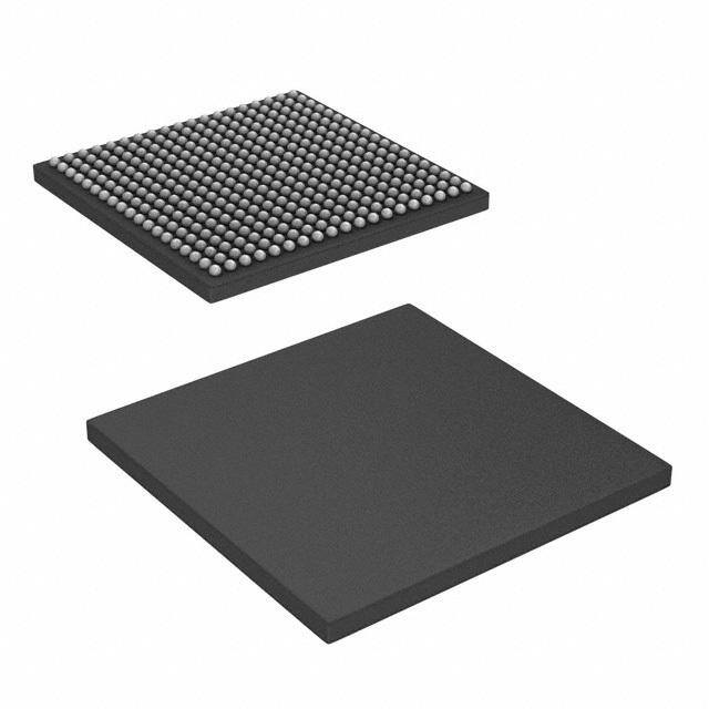
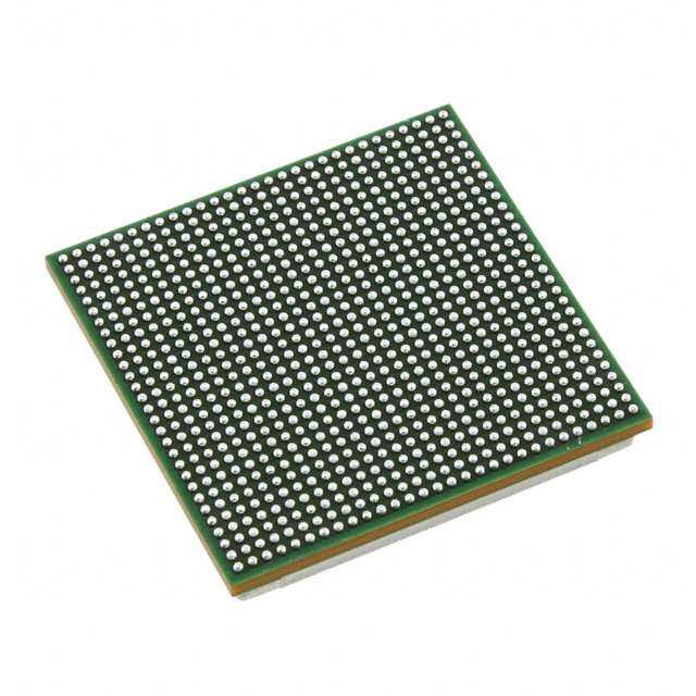
| 供应商器件封装 | 361-NFBGA(16x16) |
| 其它名称 | 296-32754 |
| 制造商产品页 | http://www.ti.com/general/docs/suppproductinfo.tsp?distId=10&orderablePartNumber=TMS320C6748BZWTA3 |
| 包装 | 托盘 |
| 商标 | Texas Instruments |
| 处理器系列 | TMS320C6x |
| 安装类型 | 表面贴装 |
| 安装风格 | SMD/SMT |
| 定时器数量 | 4 Timer |
| 封装/外壳 | 361-LFBGA |
| 封装/箱体 | nFBGA-361 |
| 工作温度 | -40°C ~ 105°C |
| 工作电源电压 | 1 V to 1.3 V, 1.8 V, 3.3 V |
| 工厂包装数量 | 90 |
| 接口 | EBI/EMI,以太网 MAC,主机接口,I²C,McASP,SPI,UART,USB |
| 接口类型 | Ethernet, I2C, MMC/SD, SATA, SPI, UART, USB, VPIF |
| 时钟速率 | 375MHz |
| 最大工作温度 | + 105 C |
| 最大时钟频率 | 456 MHz |
| 最小工作温度 | - 40 C |
| 标准包装 | 90 |
| 核心 | C674x |
| 片上ADC | No |
| 片载RAM | 448kB |
| 电压-I/O | 1.8V,3.3V |
| 电压-内核 | 1.20V |
| 程序存储器大小 | 320 kB |
| 程序存储器类型 | Cache |
| 类型 | TMS320C6x |
| 系列 | TMS320C6748 |
| 系列/芯体 | TMS320C6x |
| 芯体结构 | C674x |
| 说明书类型 | Fixed/Floating Point |
| 非易失性存储器 | 外部 |


- 商务部:美国ITC正式对集成电路等产品启动337调查
- 曝三星4nm工艺存在良率问题 高通将骁龙8 Gen1或转产台积电
- 太阳诱电将投资9.5亿元在常州建新厂生产MLCC 预计2023年完工
- 英特尔发布欧洲新工厂建设计划 深化IDM 2.0 战略
- 台积电先进制程称霸业界 有大客户加持明年业绩稳了
- 达到5530亿美元!SIA预计今年全球半导体销售额将创下新高
- 英特尔拟将自动驾驶子公司Mobileye上市 估值或超500亿美元
- 三星加码芯片和SET,合并消费电子和移动部门,撤换高东真等 CEO
- 三星电子宣布重大人事变动 还合并消费电子和移动部门
- 海关总署:前11个月进口集成电路产品价值2.52万亿元 增长14.8%

PDF Datasheet 数据手册内容提取
Product Order Technical Tools & Support & Folder Now Documents Software Community TMS320C6748 SPRS590G–JUNE2009–REVISEDJANUARY2017 TMS320C6748™ Fixed- and Floating-Point DSP 1 Device Overview 1.1 Features 1 • 375-and456-MHzC674xFixed-andFloating- – 2SP × DP→DPEveryThreeClocks PointVLIWDSP – 2DP ×DP →DPEveryFourClocks • C674xInstructionSetFeatures – Fixed-PointMultiplySupportsTwo32 ×32- – SupersetoftheC67x+andC64x+ISAs BitMultiplies,Four16 ×16-BitMultiplies,or Eight8×8-BitMultipliesperClockCycle, – Upto3648MIPSand2746MFLOPS andComplexMultiples – Byte-Addressable(8-,16-,32-,and64-BitData) – InstructionPackingReducesCodeSize – 8-BitOverflowProtection – AllInstructionsConditional – Bit-FieldExtract,Set,Clear – HardwareSupportforModuloLoopOperation – Normalization,Saturation,Bit-Counting – ProtectedModeOperation – Compact16-BitInstructions – ExceptionsSupportforErrorDetectionand • C674xTwo-LevelCacheMemoryArchitecture ProgramRedirection – 32KBofL1PProgramRAM/Cache • SoftwareSupport – 32KBofL1DDataRAM/Cache – TIDSPBIOS™ – 256KBofL2UnifiedMappedRAM/Cache – ChipSupportLibraryandDSPLibrary – FlexibleRAM/CachePartition(L1andL2) • 128KBofRAMSharedMemory • EnhancedDirectMemoryAccessController3 • 1.8-Vor3.3-VLVCMOSI/Os(Exceptfor USBand (EDMA3): DDR2Interfaces) – 2ChannelControllers • TwoExternalMemoryInterfaces: – 3TransferControllers – EMIFA – 64IndependentDMAChannels – NOR(8-or16-Bit-WideData) – 16QuickDMAChannels – NAND(8-or16-Bit-WideData) – ProgrammableTransferBurstSize – 16-BitSDRAMWith128-MBAddressSpace • TMS320C674xFloating-PointVLIWDSPCore – DDR2/MobileDDRMemoryControllerWithone – Load-StoreArchitectureWithNonaligned oftheFollowing: Support – 16-BitDDR2SDRAMWith256-MBAddress – 64General-PurposeRegisters(32-Bit) Space – SixALU(32-and40-Bit)FunctionalUnits – 16-BitmDDRSDRAMWith256-MBAddress – Supports32-BitInteger,SP(IEEESingle Space Precision/32-Bit)andDP(IEEEDouble • ThreeConfigurable16550-TypeUARTModules: Precision/64-Bit)FloatingPoint – WithModemControlSignals – SupportsuptoFourSPAdditionsPerClock, – 16-ByteFIFO FourDPAdditionsEveryTwoClocks – 16xor13xOversamplingOption – SupportsuptoTwoFloating-Point(SPorDP) • LCDController ReciprocalApproximation(RCPxP)and Square-RootReciprocalApproximation • TwoSerialPeripheralInterfaces(SPIs)EachWith (RSQRxP)OperationsPerCycle MultipleChipSelects – TwoMultiplyFunctionalUnits: • TwoMultimediaCard(MMC)/SecureDigital(SD) CardInterfacesWithSecureDataI/O(SDIO) – Mixed-PrecisionIEEEFloating-PointMultiply Interfaces Supportedupto: • TwoMasterandSlaveInter-IntegratedCircuits – 2SP × SP→SPPerClock (I2CBus™) – 2SP × SP→DPEveryTwoClocks 1 An IMPORTANT NOTICE at the end of this data sheet addresses availability, warranty, changes, use in safety-critical applications, intellectualpropertymattersandotherimportantdisclaimers.PRODUCTIONDATA.
TMS320C6748 SPRS590G–JUNE2009–REVISEDJANUARY2017 www.ti.com • OneHost-PortInterface(HPI)With16-Bit-Wide • UniversalParallelPort(uPP): MuxedAddressandDataBusForHighBandwidth – High-SpeedParallelInterfacetoFPGAsand • ProgrammableReal-TimeUnitSubsystem DataConverters (PRUSS) – DataWidthonBothChannelsis8-to16-Bit – TwoIndependentProgrammableReal-TimeUnit Inclusive (PRU)Cores – Single-DataRateorDual-DataRateTransfers – 32-BitLoad-StoreRISCArchitecture – SupportsMultipleInterfacesWithSTART, – 4KBofInstructionRAMPerCore ENABLE,andWAITControls – 512BytesofDataRAMPerCore • SerialATA(SATA)Controller: – PRUSScanbeDisabledThroughSoftwareto – SupportsSATAI(1.5Gbps)andSATAII SavePower (3.0Gbps) – Register30ofEachPRUisExportedFrom – SupportsAllSATAPower-Management theSubsysteminAdditiontotheNormalR31 Features OutputofthePRUCores. – Hardware-AssistedNativeCommandQueueing – StandardPower-ManagementMechanism (NCQ)forupto32Entries – ClockGating – SupportsPortMultiplierandCommand-Based – EntireSubsystemUnderaSinglePSCClock Switching GatingDomain • Real-TimeClock(RTC)With32-kHzOscillatorand – DedicatedInterruptController SeparatePowerRail – DedicatedSwitchedCentralResource • Three64-BitGeneral-PurposeTimers(Each ConfigurableasTwo32-BitTimers) • USB1.1OHCI(Host)WithIntegratedPHY(USB1) • One64-BitGeneral-PurposeorWatchdogTimer • USB2.0OTGPortWithIntegratedPHY(USB0) (ConfigurableasTwo32-BitGeneral-Purpose – USB2.0High-andFull-SpeedClient Timers) – USB2.0High-,Full-,andLow-SpeedHost • TwoEnhancedHigh-ResolutionPulseWidth – EndPoint0(Control) Modulators(eHRPWMs): – EndPoints1,2,3,and4(Control,Bulk, – Dedicated16-BitTime-BaseCounterWith Interrupt,orISOC)RXandTX PeriodandFrequencyControl • OneMultichannelAudioSerialPort(McASP): – 6Single-EdgeOutputs,6Dual-EdgeSymmetric – TwoClockZonesand16SerialDataPins Outputs,or3Dual-EdgeAsymmetricOutputs – SupportsTDM,I2S,andSimilarFormats – Dead-BandGeneration – DIT-Capable – PWMChoppingbyHigh-FrequencyCarrier – FIFOBuffersforTransmitandReceive – TripZoneInput • TwoMultichannelBufferedSerialPorts(McBSPs): • Three32-BitEnhancedCapture(eCAP)Modules: – SupportsTDM,I2S,andSimilarFormats – Configurableas3CaptureInputsor3Auxiliary – AC97AudioCodecInterface PulseWidthModulator(APWM)Outputs – TelecomInterfaces(ST-Bus,H100) – Single-ShotCaptureofuptoFourEvent – 128-ChannelTDM Timestamps – FIFOBuffersforTransmitandReceive • Packages: • 10/100MbpsEthernetMAC(EMAC): – 361-BallPb-FreePlasticBallGridArray(PBGA) – IEEE802.3Compliant [ZCESuffix],0.65-mmBallPitch – MIIMedia-IndependentInterface – 361-BallPb-FreePBGA[ZWTSuffix], 0.80-mmBallPitch – RMIIReducedMedia-IndependentInterface • Commercial,Extended,orIndustrialTemperature – ManagementDataI/O(MDIO)Module • VideoPortInterface(VPIF): – Two8-BitSD(BT.656),Single16-BitorSingle Raw(8-,10-,and12-Bit)VideoCapture Channels – Two8-BitSD(BT.656),Single16-BitVideo DisplayChannels 2 DeviceOverview Copyright©2009–2017,TexasInstrumentsIncorporated SubmitDocumentationFeedback ProductFolderLinks:TMS320C6748
TMS320C6748 www.ti.com SPRS590G–JUNE2009–REVISEDJANUARY2017 1.2 Applications • CurrencyInspection • MachineVision(Low-End) • BiometricIdentification 1.3 Description TheTMS320C6748fixed-andfloating-pointDSPisalow-powerapplicationsprocessorbasedonaC674x DSP core. This DSP provides significantly lower power than other members of the TMS320C6000™ platformofDSPs. The device enables original-equipment manufacturers (OEMs) and original-design manufacturers (ODMs) to quickly bring to market devices with robust operating systems, rich user interfaces, and high processor performancethroughthemaximumflexibilityofafullyintegrated,mixedprocessorsolution. The device DSP core uses a 2-level cache-based architecture. The level 1 program cache (L1P) is a 32-KB direct mapped cache, and the level 1 data cache (L1D) is a 32-KB 2-way, set-associative cache. The level 2 program cache (L2P) consists of a 256-KB memory space that is shared between program and data space. L2 memory can be configured as mapped memory, cache, or combinations of the two. Although the DSP L2 is accessible by other hosts in the system, an additional 128KB of RAM shared memoryisavailableforusebyotherhostswithoutaffectingDSPperformance. For security-enabled devices, TI’s Basic Secure Boot lets users protect proprietary intellectual property and prevents external entities from modifying user-developed algorithms. By starting from a hardware- based “root-of-trust," the secure boot flow ensures a known good starting point for code execution. By default, the JTAG port is locked down to prevent emulation and debug attacks; however, the JTAG port can be enabled during the secure boot process during application development. The boot modules are encrypted while sitting in external nonvolatile memory, such as flash or EEPROM, and are decrypted and authenticated when loaded during secure boot. Encryption and decryption protects customers’ IP and lets themsecurelysetupthesystemandbegindeviceoperationwithknown,trustedcode. Basic Secure Boot uses either SHA-1 or SHA-256, and AES-128 for boot image validation. Basic Secure Boot also uses AES-128 for boot image encryption. The secure boot flow employs a multilayer encryption scheme which not only protects the boot process but also offers the ability to securely upgrade boot and application software code. A 128-bit device-specific cipher key, known only to the device and generated using a NIST-800-22 certified random number generator, is used to protect customer encryption keys. When an update is needed, the customer uses the encryption keys to create a new encrypted image. Then the device can acquire the image through an external interface, such as Ethernet, and overwrite the existing code. For more details on the supported security features or TI’s Basic Secure Boot, see the TMS320C674x/OMAP-L1xProcessorSecurityUser’sGuide. The peripheral set includes: a 10/100 Mbps Ethernet media access controller (EMAC) with a management data input/output (MDIO) module; one USB2.0 OTG interface; one USB1.1 OHCI interface; two I2C Bus interfaces; one multichannel audio serial port (McASP) with 16 serializers and FIFO buffers; two multichannel buffered serial ports (McBSPs) with FIFO buffers; two serial peripheral interfaces (SPIs) with multiple chip selects; four 64-bit general-purpose timers each configurable (one configurable as a watchdog); a configurable 16-bit host-port interface (HPI); up to 9 banks of general-purpose input/output (GPIO) pins, with each bank containing 16 pins with programmable interrupt and event generation modes, multiplexed with other peripherals; three UART interfaces (each with RTS and CTS); two enhanced high- resolution pulse width modulator (eHRPWM) peripherals; three 32-bit enhanced capture (eCAP) module peripherals which can be configured as 3 capture inputs or 3 APWM outputs; two external memory interfaces: an asynchronous and SDRAM external memory interface (EMIFA) for slower memories or peripherals;andahigherspeedDDR2/MobileDDRcontroller. The EMAC provides an efficient interface between the device and a network. The EMAC supports both 10Base-T and 100Base-TX, or 10 Mbps and 100 Mbps in either half- or full-duplex mode. Additionally, an MDIOinterfaceisavailableforPHYconfiguration.TheEMACsupportsbothMIIandRMIIinterfaces. Copyright©2009–2017,TexasInstrumentsIncorporated DeviceOverview 3 SubmitDocumentationFeedback ProductFolderLinks:TMS320C6748
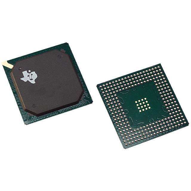
TMS320C6748 SPRS590G–JUNE2009–REVISEDJANUARY2017 www.ti.com The Serial ATA (SATA) controller provides a high-speed interface to mass data storage devices. The SATAcontrollersupportsbothSATAI(1.5Gbps)andSATAII(3.0Gbps). The Universal Parallel Port (uPP) provides a high-speed interface to many types of data converters, FPGAs, or other parallel devices. The uPP supports programmable data widths between 8- to 16-bits on bothchannels.Single-datarateanddouble-dataratetransfersaresupportedaswellasSTART,ENABLE, andWAITsignalstoprovidecontrolforavarietyofdataconverters. Avideoportinterface(VPIF)providesaflexiblevideoI/Oport. The rich peripheral set provides the ability to control external peripheral devices and communicate with external processors. For details on each peripheral, see the related sections in this document and the associatedperipheralreferenceguides. The device has a complete set of development tools for the DSP. These tools include C compilers, a DSP assembly optimizer to simplify programming and scheduling, and a Windows® debugger interface for visibilityintosourcecodeexecution. DeviceInformation(1) PARTNUMBER PACKAGE BODYSIZE TMS320C6748ZCE NFBGA(361) 13,00mmx13,00mm TMS320C6748ZWT NFBGA(361) 16,00mmx16,00mm (1) Formoreinformationonthesedevices,seeSection8. 4 DeviceOverview Copyright©2009–2017,TexasInstrumentsIncorporated SubmitDocumentationFeedback ProductFolderLinks:TMS320C6748
TMS320C6748 www.ti.com SPRS590G–JUNE2009–REVISEDJANUARY2017 1.4 Functional Block Diagram Figure1-1showsthefunctionalblockdiagramofthedevice. JTAG Interface DSPSubsystem System Control C674x™ Input PLL/Clock DSPCPU Clock(s) Generator Memory w/OSC Protection AET General- Purpose 32KB 32KB Timer (x3) Power/Sleep L1 Pgm L1 RAM Controller RTC/ 256KB L2 RAM 32-kHz Pin OSC Multiplexing BOOT ROM Switched Central Resource (SCR) Peripherals DMA Audio Ports Serial Interfaces Display Parallel Port Internal Memory Control Timers EDMA3 McASP McBSP I2C SPI UART LCD uPP 128KB ePWM eCAP (x2) w/FIFO (x2) (x2) (x2) (x3) Ctlr RAM (x2) (x3) Customizable Interface Connectivity Video External Memory Interfaces USB2.0 USB1.1 EMAC MMC/SD EMIFA(8b/16B) PRU Subsystem OTPGH YCtlr OHPCHI YCtlr (M1I0I//R10M0II) MDIO HPI ((8xb2)) SATA VPIF N16AbN SDD/FRlaAsMh DCDoRn2t/rMoDlleDrR Figure1-1.FunctionalBlockDiagram Copyright©2009–2017,TexasInstrumentsIncorporated DeviceOverview 5 SubmitDocumentationFeedback ProductFolderLinks:TMS320C6748
TMS320C6748 SPRS590G–JUNE2009–REVISEDJANUARY2017 www.ti.com Table of Contents 1 DeviceOverview ........................................ 1 6.11 DDR2/mDDRMemoryController.................. 119 .............................................. .......................... 1.1 Features 1 6.12 MemoryProtectionUnits 132 ........................................... ......... 1.2 Applications 3 6.13 MMC/SD/SDIO(MMCSD0,MMCSD1) 135 ............................................ ...................... 1.3 Description 3 6.14 SerialATAController(SATA) 138 ............................ .......... 1.4 FunctionalBlockDiagram 5 6.15 MultichannelAudioSerialPort(McASP) 143 2 Revision History......................................... 7 6.16 MultichannelBufferedSerialPort(McBSP)........ 152 3 DeviceComparison ..................................... 8 6.17 SerialPeripheralInterfacePorts(SPI0,SPI1)..... 161 ................................ .......... 3.1 Device Characteristics 8 6.18 Inter-IntegratedCircuitSerialPorts(I2C) 182 3.2 Device Compatibility.................................. 9 6.19 UniversalAsynchronousReceiver/Transmitter ............................................. ...................................... (UART) 186 3.3 DSPSubsystem 9 ............................. 6.20 UniversalSerialBusOTGController(USB0) 3.4 MemoryMapSummary 20 ..................................... [USB2.0OTG] 188 .................................... 3.5 PinAssignments 23 6.21 UniversalSerialBusHostController(USB1) 3.6 PinMultiplexingControl............................. 26 [USB1.1OHCI]..................................... 195 3.7 TerminalFunctions.................................. 27 6.22 EthernetMediaAccessController(EMAC)........ 196 3.8 UnusedPinConfigurations.......................... 69 6.23 ManagementDataInput/Output(MDIO)........... 203 4 DeviceConfiguration.................................. 71 6.24 LCDController(LCDC)............................ 205 4.1 BootModes ......................................... 71 6.25 Host-PortInterface(UHPI)......................... 220 4.2 SYSCFG Module.................................... 71 6.26 UniversalParallelPort(uPP)...................... 228 4.3 Pullup/Pulldown Resistors .......................... 74 6.27 VideoPortInterface(VPIF)........................ 233 5 Specifications........................................... 75 6.28 EnhancedCapture(eCAP)Peripheral............. 239 5.1 AbsoluteMaximumRatingsOverOperating 6.29 EnhancedHigh-ResolutionPulse-WidthModulator JunctionTemperatureRange ......................................... (eHRPWM) 242 ................................. (UnlessOtherwiseNoted) 75 .............................................. 6.30 Timers 247 .................................... 5.2 Handling Ratings 75 ............................ 6.31 RealTimeClock(RTC) 249 ............... 5.3 RecommendedOperatingConditions 76 ............. 6.32 General-PurposeInput/Output(GPIO) 252 . 5.4 NotesonRecommendedPower-OnHours(POH) 78 6.33 ProgrammableReal-TimeUnitSubsystem 5.5 ElectricalCharacteristicsOverRecommended ........................................... (PRUSS) 256 RangesofSupplyVoltageandOperatingJunction .................................... ............ 6.34 EmulationLogic 259 Temperature(UnlessOtherwiseNoted) 79 7 DeviceandDocumentationSupport.............. 263 6 PeripheralInformationandElectrical Specifications........................................... 80 7.1 Device Nomenclature.............................. 263 6.1 ParameterInformation .............................. 80 7.2 ToolsandSoftware................................ 264 ............................ 6.2 RecommendedClockandControlSignalTransition 7.3 DocumentationSupport 264 Behavior............................................. 81 7.4 CommunityResources............................. 265 6.3 PowerSupplies...................................... 81 7.5 Trademarks........................................ 265 6.4 Reset................................................ 82 7.6 ElectrostaticDischargeCaution................... 265 6.5 CrystalOscillatororExternalClockInput........... 86 7.7 ExportControlNotice.............................. 265 6.6 ClockPLLs.......................................... 87 7.8 Glossary............................................ 265 ............................................ 6.7 Interrupts 92 8 MechanicalPackagingandOrderable 6.8 PowerandSleepController(PSC).................. 96 Information............................................. 266 6.9 EnhancedDirectMemoryAccessController 8.1 ThermalDataforZCEPackage................... 266 ........................................... (EDMA3) 101 ................... 8.2 ThermalDataforZWTPackage 267 ............. 6.10 ExternalMemoryInterfaceA(EMIFA) 107 ............................. 8.3 PackagingInformation 267 6 TableofContents Copyright©2009–2017,TexasInstrumentsIncorporated SubmitDocumentationFeedback ProductFolderLinks:TMS320C6748
TMS320C6748 www.ti.com SPRS590G–JUNE2009–REVISEDJANUARY2017 2 Revision History NOTE:Pagenumbersforpreviousrevisionsmaydifferfrompagenumbersinthecurrentversion. ChangesfromMarch31,2014toJanuary31,2017 Page • RemovedinternalpullupdesignationfromRESETinTable3-5.............................................................. 27 • AddedfootnotetoCLKOUTDescriptioninTable3-6.......................................................................... 28 • AddednewcolumntoTable3-32called"Configuration(WhenUSB1isusedandUSB0isnotused)"................ 69 Copyright©2009–2017,TexasInstrumentsIncorporated RevisionHistory 7 SubmitDocumentationFeedback ProductFolderLinks:TMS320C6748
TMS320C6748 SPRS590G–JUNE2009–REVISEDJANUARY2017 www.ti.com 3 Device Comparison 3.1 Device Characteristics Table 3-1 provides an overview of the device. The table shows significant features of the device, including thecapacityofon-chipRAM,peripherals,andthepackagetypewithpincount. Table3-1.CharacteristicsofC6748 HARDWAREFEATURES C6748 DDR2,16-bitbuswidth,upto156MHz DDR2/mDDRMemoryController MobileDDR,16-bitbuswidth,upto150MHz Asynchronous(8/16-bitbuswidth)RAM,Flash, EMIFA 16-bitSDRAM,NOR,NAND FlashCardInterface 2MMCandSDcardssupported 64independentchannels,16QDMAchannels, EDMA3 2channelcontrollers,3transfercontrollers 464-BitGeneralPurpose(eachconfigurableas2separate Timers 32-bittimers,oneconfigurableasWatchDog) UART 3(eachwithRTSandCTSflowcontrol) SPI 2(Eachwithonehardwarechipselect) I2C 2(bothMaster/Slave) Peripherals MultichannelAudioSerialPort[McASP] 1(eachwithtransmit/receive,FIFObuffer,16serializers) Notallperipheralspins MultichannelBufferedSerialPort[McBSP] 2(eachwithtransmit/receive,FIFObuffer,16) areavailableatthe sametime(formore 10/100EthernetMACwithManagementDataI/O 1(MIIorRMIIInterface) detail,seetheDevice 4SingleEdge,4DualEdgeSymmetric,or Configurationssection). eHRPWM 2DualEdgeAsymmetricOutputs eCAP 332-bitcaptureinputsor332-bitauxiliaryPWMoutputs UHPI 1(16-bitmultiplexedaddress/data) USB2.0(USB0) High-SpeedOTGControllerwithon-chipOTGPHY USB1.1(USB1) Full-SpeedOHCI(ashost)withon-chipPHY General-PurposeInput/OutputPort 9banksof16-bit LCDController 1 SATAController 1(SupportsbothSATAIandSATAII) UniversalParallelPort(uPP) 1 VideoPortInterface(VPIF) 1(videoinandvideoout) PRUSubsystem(PRUSS) 2ProgrammablePRUCores Size(Bytes) 448KBRAM DSP 32KBL1Program(L1P)/Cache(upto32KB) 32KBL1Data(L1D)/Cache(upto32KB) 256KBUnifiedMappedRAM/Cache(L2) On-ChipMemory Organization DSPMemoriescanbemadeaccessibletoEDMA3and otherperipherals. ADDITIONALMEMORY 128KBRAM Security SecureBoot TIBasicSecureBoot C674xCPUID+CPU ControlStatusRegister(CSR.[31:16]) 0x1400 RevID C674xMegamodule RevisionIDRegister(MM_REVID[15:0]) 0x0000 Revision JTAGBSDL_ID DEVIDR0Register seeSection6.34.4.1,JTAGPeripheralRegisterDescription CPUFrequency MHz 674xDSP375MHz(1.2V)or456MHz(1.3V) 8 DeviceComparison Copyright©2009–2017,TexasInstrumentsIncorporated SubmitDocumentationFeedback ProductFolderLinks:TMS320C6748
TMS320C6748 www.ti.com SPRS590G–JUNE2009–REVISEDJANUARY2017 Table3-1.CharacteristicsofC6748 (continued) HARDWAREFEATURES C6748 Variable(1.2V-1.0V)for375MHzversion Core(V) Voltage Variable(1.3V-1.0V)for456MHzversion I/O(V) 1.8Vor3.3V 13mmx13mm,361-Ball0.65mmpitch,PBGA(ZCE) Packages 16mmx16mm,361-Ball0.80mmpitch,PBGA(ZWT) ProductPreview(PP), ProductStatus(1) AdvanceInformation(AI), 375MHzversions-PD 456MHzversions-PD orProductionData(PD) (1) ADVANCEINFORMATIONconcernsnewproductsinthesamplingorpreproductionphaseofdevelopment.Characteristicdataand otherspecificationsaresubjecttochangewithoutnotice.PRODUCTIONDATAinformationiscurrentasofpublicationdate.Products conformtospecificationsperthetermsoftheTexasInstrumentsstandardwarranty.Productionprocessingdoesnotnecessarilyinclude testingofallparameters. 3.2 Device Compatibility The C674x DSP core is code-compatible with the C6000™ DSP platform and supports features of both theC64x+andC67x+DSPfamilies. 3.3 DSP Subsystem TheDSPSubsystemincludesthefollowingfeatures: • C674xDSPCPU • 32KBL1Program(L1P)/Cache(upto32KB) • 32KBL1Data(L1D)/Cache(upto32KB) • 256KBUnifiedMappedRAM/Cache(L2) • BootROM (cannotbeusedforapplicationcode) • Littleendian Copyright©2009–2017,TexasInstrumentsIncorporated DeviceComparison 9 SubmitDocumentationFeedback ProductFolderLinks:TMS320C6748
TMS320C6748 SPRS590G–JUNE2009–REVISEDJANUARY2017 www.ti.com 32K Bytes 256K Bytes BOOT L1PRAM/ L2 RAM ROM Cache 256 256 256 256 Cache Control Cache Control Memory Protect L1P Memory Protect L2 Bandwidth Mgmt Bandwidth Mgmt 256 256 256 256 Power Down Instruction Fetch Interrupt Controller C674x Fixed/Floating Point CPU IDMA Register Register FileA File B 256 64 64 CFG Bandwidth Mgmt Memory Protect L1D EMC 32 Configuration Peripherals Cache Control Bus MDMA SDMA 8 x 32 64 64 64 64 32K Bytes High L1D RAM/ Performance Cache Switch Fabric Figure3-1.C674xMegamoduleBlockDiagram 3.3.1 C674x DSP CPU Description The C674x Central Processing Unit (CPU) consists of eight functional units, two register files, and two data paths as shown in Figure 3-2. The two general-purpose register files (A and B) each contain 32 32- bit registers for a total of 64 registers. The general-purpose registers can be used for data or can be data address pointers. The data types supported include packed 8-bit data, packed 16-bit data, 32-bit data, 40- bit data, and 64-bit data. Values larger than 32 bits, such as 40-bit-long or 64-bit-long values are stored in register pairs, with the 32 LSBs of data placed in an even register and the remaining 8 or 32 MSBs in the nextupperregister(whichisalwaysanodd-numberedregister). The eight functional units (.M1, .L1, .D1, .S1, .M2, .L2, .D2, and .S2) are each capable of executing one instruction every clock cycle. The .M functional units perform all multiply operations. The .S and .L units perform a general set of arithmetic, logical, and branch functions. The .D units primarily load data from memorytotheregisterfileandstoreresultsfromtheregisterfileintomemory. The C674x CPU combines the performance of the C64x+ core with the floating-point capabilities of the C67x+core. 10 DeviceComparison Copyright©2009–2017,TexasInstrumentsIncorporated SubmitDocumentationFeedback ProductFolderLinks:TMS320C6748
TMS320C6748 www.ti.com SPRS590G–JUNE2009–REVISEDJANUARY2017 Each C674x .M unit can perform one of the following each clock cycle: one 32 x 32 bit multiply, one 16 x 32 bit multiply, two 16 x 16 bit multiplies, two 16 x 32 bit multiplies, two 16 x 16 bit multiplies with add/subtract capabilities, four 8 x 8 bit multiplies, four 8 x 8 bit multiplies with add operations, and four 16 x 16 multiplies with add/subtract capabilities (including a complex multiply). There is also support for Galois field multiplication for 8-bit and 32-bit data. Many communications algorithms such as FFTs and modems require complex multiplication. The complex multiply (CMPY) instruction takes for 16-bit inputs and produces a 32-bit real and a 32-bit imaginary output. There are also complex multiplies with rounding capability that produces one 32-bit packed output that contain 16-bit real and 16-bit imaginary values. The 32 x 32 bit multiply instructions provide the extended precision necessary for high-precision algorithms on avarietyofsignedandunsigned32-bitdatatypes. The .L or (Arithmetic Logic Unit) now incorporates the ability to do parallel add/subtract operations on a pair of common inputs. Versions of this instruction exist to work on 32-bit data or on pairs of 16-bit data performingdual16-bitaddandsubtractsinparallel.Therearealsosaturatedformsoftheseinstructions. The C674x core enhances the .S unit in several ways. On the previous cores, dual 16-bit MIN2 and MAX2 comparisons were only available on the .L units. On the C674x core they are also available on the .S unit which increases the performance of algorithms that do searching and sorting. Finally, to increase data packing and unpacking throughput, the .S unit allows sustained high performance for the quad 8-bit/16-bit and dual 16-bit instructions. Unpack instructions prepare 8-bit data for parallel 16-bit operations. Pack instructionsreturnparallelresultstooutputprecisionincludingsaturationsupport. Othernewfeaturesinclude: • SPLOOP-AsmallinstructionbufferintheCPUthataidsincreationofsoftwarepipeliningloopswhere multiple iterations of a loop are executed in parallel. The SPLOOP buffer reduces the code size associatedwithsoftwarepipelining.Furthermore,loopsintheSPLOOPbufferarefullyinterruptible. • Compact Instructions - The native instruction size for the C6000 devices is 32 bits. Many common instructions such as MPY, AND, OR, ADD, and SUB can be expressed as 16 bits if the C674x compiler can restrict the code to use certain registers in the register file. This compression is performedbythecodegenerationtools. • Instruction Set Enhancement - As noted above, there are new instructions such as 32-bit multiplications, complex multiplications, packing, sorting, bit manipulation, and 32-bit Galois field multiplication. • Exceptions Handling - Intended to aid the programmer in isolating bugs. The C674x CPU is able to detect and respond to exceptions, both from internally detected sources (such as illegal op-codes) and fromsystemevents(suchasawatchdogtimeexpiration). • Privilege - Defines user and supervisor modes of operation, allowing the operating system to give a basic level of protection to sensitive resources. Local memory is divided into multiple pages, each with read,write,andexecutepermissions. • Time-Stamp Counter - Primarily targeted for Real-Time Operating System (RTOS) robustness, a free- runningtime-stampcounterisimplementedintheCPUwhichisnotsensitivetosystemstalls. For more details on the C674x CPU and its enhancements over the C64x architecture, see the following documents: • TMS320C64x/C64x+DSPCPUandInstructionSetReferenceGuide (literaturenumberSPRUFE8) • TMS320C64xTechnicalOverview(literaturenumberSPRU395) Copyright©2009–2017,TexasInstrumentsIncorporated DeviceComparison 11 SubmitDocumentationFeedback ProductFolderLinks:TMS320C6748
TMS320C6748 SPRS590G–JUNE2009–REVISEDJANUARY2017 www.ti.com ÁÁÁ ÁÁÁÁ Even src1 Odd register ÁÁÁÁÁÁ register file A file A (A0, A2, .L1 srcÁ2 ÁÁ ÁÁ (A1, A3, A4...A30) A5...A31) odd dsÁt Á ÁÁ (D) even dst long src 8 ÁÁ ST1b 32 MSB 32 LSB ST1a long src 8 Á even dst Á Á Data path A odd dst (D) .S1 src1 ÁÁ Á src2 ÁÁ ÁÁ 32 dst2 ÁÁÁ ÁÁ (A) dst1 32 (B) .M1 src1 ÁÁ ÁÁ src2 ÁÁ Á (C) 32 MSB LD1b 32 LÁSB Á Á LD1a Á dst Á .D1 src1 DA1Á Á src2 2x ÁÁ 1x Even Á Á Odd register DA2Á .D2 ssrrcc12 Á refigleis tBer (Bfi0le, BB2, dst Á (B1, B3, B4...B30) LD2a 32 LSB B5...B31) LD2b 32 MSB Á Á src2 (C) .M2 src1 ÁÁ dst2 32 (B) dst1 32 ÁÁ (A) ÁÁ src2 src1 Á Data path B .S2 odd dst Á (D) even dst 8 long src Á 32 MSB ST2a 32 LSB ST2b Á 8 long src ÁÁ even dst ÁÁ (D) odd dst .L2 ÁÁ src2 src1 Control Register A. On .M unit, dst2 is 32 MSB. B. On .M unit, dst1 is 32 LSB. C. On C64x CPU .M unit, src2 is 32 bits; on C64x+ CPU .M unit, src2 is 64 bits. D. On .L and .S units, odd dst connects to odd register files and even dst connects to even register files. Figure3-2.TMS320C674xCPU(DSPCore)DataPaths 12 DeviceComparison Copyright©2009–2017,TexasInstrumentsIncorporated SubmitDocumentationFeedback ProductFolderLinks:TMS320C6748
TMS320C6748 www.ti.com SPRS590G–JUNE2009–REVISEDJANUARY2017 3.3.2 DSP Memory Mapping TheDSPmemorymapisshowninSection3.4. BydefaulttheDSPalsohasaccesstomostonandoffchipmemoryareas. Additionally, the DSP megamodule includes the capability to limit access to its internal memories through itsSDMAport;withoutneedinganexternalMPUunit. 3.3.2.1 ExternalMemories TheDSPhasaccesstothefollowingExternalmemories: • AsynchronousEMIF/SDRAM/NAND/NORFlash(EMIFA) • SDRAM(DDR2) 3.3.2.2 DSPInternalMemories TheDSPhasaccesstothefollowingDSPmemories: • L2RAM • L1PRAM • L1DRAM 3.3.2.3 C674xCPU The C674x core uses a two-level cache-based architecture. The Level 1 Program cache (L1P) is 32 KB directmappedcacheandtheLevel1Datacache(L1D)is32KB2-waysetassociatedcache.TheLevel2 memory/cache (L2) consists of a 256 KB memory space that is shared between program and data space. L2memorycanbeconfiguredasmappedmemory,cache,oracombinationofboth. Table3-2showsamemorymapoftheC674xCPUcacheregistersforthedevice. Table3-2.C674xCacheRegisters ByteAddress RegisterName RegisterDescription 0x01840000 L2CFG L2Cacheconfigurationregister 0x01840020 L1PCFG L1PSizeCacheconfigurationregister 0x01840024 L1PCC L1PFreezeModeCacheconfigurationregister 0x01840040 L1DCFG L1DSizeCacheconfigurationregister 0x01840044 L1DCC L1DFreezeModeCacheconfigurationregister 0x01840048-0x01840FFC - Reserved 0x01841000 EDMAWEIGHT L2EDMAaccesscontrolregister 0x01841004-0x01841FFC - Reserved 0x01842000 L2ALLOC0 L2allocationregister0 0x01842004 L2ALLOC1 L2allocationregister1 0x01842008 L2ALLOC2 L2allocationregister2 0x0184200C L2ALLOC3 L2allocationregister3 0x01842010-0x01843FFF - Reserved 0x01844000 L2WBAR L2writebackbaseaddressregister 0x01844004 L2WWC L2writebackwordcountregister 0x01844010 L2WIBAR L2writebackinvalidatebaseaddressregister 0x01844014 L2WIWC L2writebackinvalidatewordcountregister 0x01844018 L2IBAR L2invalidatebaseaddressregister 0x0184401C L2IWC L2invalidatewordcountregister 0x01844020 L1PIBAR L1Pinvalidatebaseaddressregister 0x01844024 L1PIWC L1Pinvalidatewordcountregister 0x01844030 L1DWIBAR L1Dwritebackinvalidatebaseaddressregister Copyright©2009–2017,TexasInstrumentsIncorporated DeviceComparison 13 SubmitDocumentationFeedback ProductFolderLinks:TMS320C6748
TMS320C6748 SPRS590G–JUNE2009–REVISEDJANUARY2017 www.ti.com Table3-2.C674xCacheRegisters(continued) ByteAddress RegisterName RegisterDescription 0x01844034 L1DWIWC L1Dwritebackinvalidatewordcountregister 0x01844038 - Reserved 0x01844040 L1DWBAR L1DBlockWriteback 0x01844044 L1DWWC L1DBlockWriteback 0x01844048 L1DIBAR L1Dinvalidatebaseaddressregister 0x0184404C L1DIWC L1Dinvalidatewordcountregister 0x01844050-0x01844FFF - Reserved 0x01845000 L2WB L2writebackallregister 0x01845004 L2WBINV L2writebackinvalidateallregister 0x01845008 L2INV L2GlobalInvalidatewithoutwriteback 0x0184500C-0x01845027 - Reserved 0x01845028 L1PINV L1PGlobalInvalidate 0x0184502C-0x01845039 - Reserved 0x01845040 L1DWB L1DGlobalWriteback 0x01845044 L1DWBINV L1DGlobalWritebackwithInvalidate 0x01845048 L1DINV L1DGlobalInvalidatewithoutwriteback 0x01848000–0x018480FF MAR0-MAR63 Reserved0x00000000–0x3FFFFFFF MemoryAttributeRegistersforEMIFASDRAMData(CS0) 0x01848100–0x0184817F MAR64–MAR95 Externalmemoryaddresses0x40000000–0x5FFFFFFF MemoryAttributeRegistersforEMIFAAsyncData(CS2) 0x01848180–0x01848187 MAR96-MAR97 Externalmemoryaddresses0x60000000–0x61FFFFFF MemoryAttributeRegistersforEMIFAAsyncData(CS3) 0x01848188–0x0184818F MAR98–MAR99 Externalmemoryaddresses0x62000000–0x63FFFFFF MemoryAttributeRegistersforEMIFAAsyncData(CS4) 0x01848190–0x01848197 MAR100–MAR101 Externalmemoryaddresses0x64000000–0x65FFFFFF MemoryAttributeRegistersforEMIFAAsyncData(CS5) 0x01848198–0x0184819F MAR102–MAR103 Externalmemoryaddresses0x66000000–0x67FFFFFF 0x018481A0–0x018481FF MAR104–MAR127 Reserved0x68000000–0x7FFFFFFF MemoryAttributeRegisterforRAM 0x01848200 MAR128 Externalmemoryaddresses0x80000000–0x8001FFFF Reserved0x80020000–0x81FFFFFF 0x01848204–0x018482FF MAR129–MAR191 Reserved0x82000000–0xBFFFFFFF MemoryAttributeRegistersforDDR2Data(CS2) 0x01848300–0x0184837F MAR192–MAR223 Externalmemoryaddresses0xC0000000–0xDFFFFFFF 0x01848380–0x018483FF MAR224–MAR255 Reserved0xE0000000–0xFFFFFFFF Table3-3.C674xL1/L2MemoryProtectionRegisters HEXADDRESSRANGE REGISTERACRONYM DESCRIPTION 0x0184A000 L2MPFAR L2memoryprotectionfaultaddressregister 0x0184A004 L2MPFSR L2memoryprotectionfaultstatusregister 0x0184A008 L2MPFCR L2memoryprotectionfaultcommandregister 0x0184A00C-0x0184A0FF - Reserved 0x0184A100 L2MPLK0 L2memoryprotectionlockkeybits[31:0] 0x0184A104 L2MPLK1 L2memoryprotectionlockkeybits[63:32] 0x0184A108 L2MPLK2 L2memoryprotectionlockkeybits[95:64] 0x0184A10C L2MPLK3 L2memoryprotectionlockkeybits[127:96] 0x0184A110 L2MPLKCMD L2memoryprotectionlockkeycommandregister 0x0184A114 L2MPLKSTAT L2memoryprotectionlockkeystatusregister 0x0184A118-0x0184A1FF - Reserved 14 DeviceComparison Copyright©2009–2017,TexasInstrumentsIncorporated SubmitDocumentationFeedback ProductFolderLinks:TMS320C6748
TMS320C6748 www.ti.com SPRS590G–JUNE2009–REVISEDJANUARY2017 Table3-3.C674xL1/L2MemoryProtectionRegisters(continued) HEXADDRESSRANGE REGISTERACRONYM DESCRIPTION L2memoryprotectionpageattributeregister0(controlsmemoryaddress 0x0184A200 L2MPPA0 0x00800000-0x00801FFF) L2memoryprotectionpageattributeregister1(controlsmemoryaddress 0x0184A204 L2MPPA1 0x00802000-0x00803FFF) L2memoryprotectionpageattributeregister2(controlsmemoryaddress 0x0184A208 L2MPPA2 0x00804000-0x00805FFF) L2memoryprotectionpageattributeregister3(controlsmemoryaddress 0x0184A20C L2MPPA3 0x00806000-0x00807FFF) L2memoryprotectionpageattributeregister4(controlsmemoryaddress 0x0184A210 L2MPPA4 0x00808000-0x00809FFF) L2memoryprotectionpageattributeregister5(controlsmemoryaddress 0x0184A214 L2MPPA5 0x0080A000-0x0080BFFF) L2memoryprotectionpageattributeregister6(controlsmemoryaddress 0x0184A218 L2MPPA6 0x0080C000-0x0080DFFF) L2memoryprotectionpageattributeregister7(controlsmemoryaddress 0x0184A21C L2MPPA7 0x0080E000-0x0080FFFF) L2memoryprotectionpageattributeregister8(controlsmemoryaddress 0x0184A220 L2MPPA8 0x00810000-0x00811FFF) L2memoryprotectionpageattributeregister9(controlsmemoryaddress 0x0184A224 L2MPPA9 0x00812000-0x00813FFF) L2memoryprotectionpageattributeregister10(controlsmemoryaddress 0x0184A228 L2MPPA10 0x00814000-0x00815FFF) L2memoryprotectionpageattributeregister11(controlsmemoryaddress 0x0184A22C L2MPPA11 0x00816000-0x00817FFF) L2memoryprotectionpageattributeregister12(controlsmemoryaddress 0x0184A230 L2MPPA12 0x00818000-0x00819FFF) L2memoryprotectionpageattributeregister13(controlsmemoryaddress 0x0184A234 L2MPPA13 0x0081A000-0x0081BFFF) L2memoryprotectionpageattributeregister14(controlsmemoryaddress 0x0184A238 L2MPPA14 0x0081C000-0x0081DFFF) L2memoryprotectionpageattributeregister15(controlsmemoryaddress 0x0184A23C L2MPPA15 0x0081E000-0x0081FFFF) L2memoryprotectionpageattributeregister16(controlsmemoryaddress 0x0184A240 L2MPPA16 0x00820000-0x00821FFF) L2memoryprotectionpageattributeregister17(controlsmemoryaddress 0x0184A244 L2MPPA17 0x00822000-0x00823FFF) L2memoryprotectionpageattributeregister18(controlsmemoryaddress 0x0184A248 L2MPPA18 0x00824000-0x00825FFF) L2memoryprotectionpageattributeregister19(controlsmemoryaddress 0x0184A24C L2MPPA19 0x00826000-0x00827FFF) L2memoryprotectionpageattributeregister20(controlsmemoryaddress 0x0184A250 L2MPPA20 0x00828000-0x00829FFF) L2memoryprotectionpageattributeregister21(controlsmemoryaddress 0x0184A254 L2MPPA21 0x0082A000-0x0082BFFF) L2memoryprotectionpageattributeregister22(controlsmemoryaddress 0x0184A258 L2MPPA22 0x0082C000-0x0082DFFF) L2memoryprotectionpageattributeregister23(controlsmemoryaddress 0x0184A25C L2MPPA23 0x0082E000-0x0082FFFF) L2memoryprotectionpageattributeregister24(controlsmemoryaddress 0x0184A260 L2MPPA24 0x00830000-0x00831FFF) L2memoryprotectionpageattributeregister25(controlsmemoryaddress 0x0184A264 L2MPPA25 0x00832000-0x00833FFF) L2memoryprotectionpageattributeregister26(controlsmemoryaddress 0x0184A268 L2MPPA26 0x00834000-0x00835FFF) L2memoryprotectionpageattributeregister27(controlsmemoryaddress 0x0184A26C L2MPPA27 0x00836000-0x00837FFF) Copyright©2009–2017,TexasInstrumentsIncorporated DeviceComparison 15 SubmitDocumentationFeedback ProductFolderLinks:TMS320C6748
TMS320C6748 SPRS590G–JUNE2009–REVISEDJANUARY2017 www.ti.com Table3-3.C674xL1/L2MemoryProtectionRegisters(continued) HEXADDRESSRANGE REGISTERACRONYM DESCRIPTION L2memoryprotectionpageattributeregister28(controlsmemoryaddress 0x0184A270 L2MPPA28 0x00838000-0x00839FFF) L2memoryprotectionpageattributeregister29(controlsmemoryaddress 0x0184A274 L2MPPA29 0x0083A000-0x0083BFFF) L2memoryprotectionpageattributeregister30(controlsmemoryaddress 0x0184A278 L2MPPA30 0x0083C000-0x0083DFFF) L2memoryprotectionpageattributeregister31(controlsmemoryaddress 0x0184A27C L2MPPA31 0x0083E000-0x0083FFFF) L2memoryprotectionpageattributeregister32(controlsmemoryaddress 0x0184A280 L2MPPA32 0x00700000-0x00707FFF) L2memoryprotectionpageattributeregister33(controlsmemoryaddress 0x0184A284 L2MPPA33 0x00708000-0x0070FFFF) L2memoryprotectionpageattributeregister34(controlsmemoryaddress 0x0184A288 L2MPPA34 0x00710000-0x00717FFF) L2memoryprotectionpageattributeregister35(controlsmemoryaddress 0x0184A28C L2MPPA35 0x00718000-0x0071FFFF) L2memoryprotectionpageattributeregister36(controlsmemoryaddress 0x0184A290 L2MPPA36 0x00720000-0x00727FFF) L2memoryprotectionpageattributeregister37(controlsmemoryaddress 0x0184A294 L2MPPA37 0x00728000-0x0072FFFF) L2memoryprotectionpageattributeregister38(controlsmemoryaddress 0x0184A298 L2MPPA38 0x00730000-0x00737FFF) L2memoryprotectionpageattributeregister39(controlsmemoryaddress 0x0184A29C L2MPPA39 0x00738000-0x0073FFFF) L2memoryprotectionpageattributeregister40(controlsmemoryaddress 0x0184A2A0 L2MPPA40 0x00740000-0x00747FFF) L2memoryprotectionpageattributeregister41(controlsmemoryaddress 0x0184A2A4 L2MPPA41 0x00748000-0x0074FFFF) L2memoryprotectionpageattributeregister42(controlsmemoryaddress 0x0184A2A8 L2MPPA42 0x00750000-0x00757FFF) L2memoryprotectionpageattributeregister43(controlsmemoryaddress 0x0184A2AC L2MPPA43 0x00758000-0x0075FFFF) L2memoryprotectionpageattributeregister44(controlsmemoryaddress 0x0184A2B0 L2MPPA44 0x00760000-0x00767FFF) L2memoryprotectionpageattributeregister45(controlsmemoryaddress 0x0184A2B4 L2MPPA45 0x00768000-0x0076FFFF) L2memoryprotectionpageattributeregister46(controlsmemoryaddress 0x0184A2B8 L2MPPA46 0x00770000-0x00777FFF) L2memoryprotectionpageattributeregister47(controlsmemoryaddress 0x0184A2BC L2MPPA47 0x00778000-0x0077FFFF) L2memoryprotectionpageattributeregister48(controlsmemoryaddress 0x0184A2C0 L2MPPA48 0x00780000-0x00787FFF) L2memoryprotectionpageattributeregister49(controlsmemoryaddress 0x0184A2C4 L2MPPA49 0x00788000-0x0078FFFF) L2memoryprotectionpageattributeregister50(controlsmemoryaddress 0x0184A2C8 L2MPPA50 0x00790000-0x00797FFF) L2memoryprotectionpageattributeregister51(controlsmemoryaddress 0x0184A2CC L2MPPA51 0x00798000-0x0079FFFF) L2memoryprotectionpageattributeregister52(controlsmemoryaddress 0x0184A2D0 L2MPPA52 0x007A0000-0x007A7FFF) L2memoryprotectionpageattributeregister53(controlsmemoryaddress 0x0184A2D4 L2MPPA53 0x007A8000-0x007AFFFF) L2memoryprotectionpageattributeregister54(controlsmemoryaddress 0x0184A2D8 L2MPPA54 0x007B0000-0x007B7FFF) L2memoryprotectionpageattributeregister55(controlsmemoryaddress 0x0184A2DC L2MPPA55 0x007B8000-0x007BFFFF) 16 DeviceComparison Copyright©2009–2017,TexasInstrumentsIncorporated SubmitDocumentationFeedback ProductFolderLinks:TMS320C6748
TMS320C6748 www.ti.com SPRS590G–JUNE2009–REVISEDJANUARY2017 Table3-3.C674xL1/L2MemoryProtectionRegisters(continued) HEXADDRESSRANGE REGISTERACRONYM DESCRIPTION L2memoryprotectionpageattributeregister56(controlsmemoryaddress 0x0184A2E0 L2MPPA56 0x007C0000-0x007C7FFF) L2memoryprotectionpageattributeregister57(controlsmemoryaddress 0x0184A2E4 L2MPPA57 0x007C8000-0x007CFFFF) L2memoryprotectionpageattributeregister58(controlsmemoryaddress 0x0184A2E8 L2MPPA58 0x007D0000-0x007D7FFF) L2memoryprotectionpageattributeregister59(controlsmemoryaddress 0x0184A2EC L2MPPA59 0x007D8000-0x007DFFFF) L2memoryprotectionpageattributeregister60(controlsmemoryaddress 0x0184A2F0 L2MPPA60 0x007E0000-0x007E7FFF) L2memoryprotectionpageattributeregister61(controlsmemoryaddress 0x0184A2F4 L2MPPA61 0x007E8000-0x007EFFFF) L2memoryprotectionpageattributeregister62(controlsmemoryaddress 0x0184A2F8 L2MPPA62 0x007F0000-0x007F7FFF) L2memoryprotectionpageattributeregister63(controlsmemoryaddress 0x0184A2FC L2MPPA63 0x007F8000-0x007FFFFF) 0x0184A300-0x0184A3FF - Reserved 0x0184A400 L1PMPFAR L1Pmemoryprotectionfaultaddressregister 0x0184A404 L1PMPFSR L1Pmemoryprotectionfaultstatusregister 0x0184A408 L1PMPFCR L1Pmemoryprotectionfaultcommandregister 0x0184A40C-0x0184A4FF - Reserved 0x0184A500 L1PMPLK0 L1Pmemoryprotectionlockkeybits[31:0] 0x0184A504 L1PMPLK1 L1Pmemoryprotectionlockkeybits[63:32] 0x0184A508 L1PMPLK2 L1Pmemoryprotectionlockkeybits[95:64] 0x0184A50C L1PMPLK3 L1Pmemoryprotectionlockkeybits[127:96] 0x0184A510 L1PMPLKCMD L1Pmemoryprotectionlockkeycommandregister 0x0184A514 L1PMPLKSTAT L1Pmemoryprotectionlockkeystatusregister 0x0184A518-0x0184A5FF - Reserved 0x0184A600-0x0184A63F - Reserved (1) L1Pmemoryprotectionpageattributeregister16(controlsmemoryaddress 0x0184A640 L1PMPPA16 0x00E00000-0x00E007FF) L1Pmemoryprotectionpageattributeregister17(controlsmemoryaddress 0x0184A644 L1PMPPA17 0x00E00800-0x00E00FFF) L1Pmemoryprotectionpageattributeregister18(controlsmemoryaddress 0x0184A648 L1PMPPA18 0x00E01000-0x00E017FF) L1Pmemoryprotectionpageattributeregister19(controlsmemoryaddress 0x0184A64C L1PMPPA19 0x00E01800-0x00E01FFF) L1Pmemoryprotectionpageattributeregister20(controlsmemoryaddress 0x0184A650 L1PMPPA20 0x00E02000-0x00E027FF) L1Pmemoryprotectionpageattributeregister21(controlsmemoryaddress 0x0184A654 L1PMPPA21 0x00E02800-0x00E02FFF) L1Pmemoryprotectionpageattributeregister22(controlsmemoryaddress 0x0184A658 L1PMPPA22 0x00E03000-0x00E037FF) L1Pmemoryprotectionpageattributeregister23(controlsmemoryaddress 0x0184A65C L1PMPPA23 0x00E03800-0x00E03FFF) L1Pmemoryprotectionpageattributeregister24(controlsmemoryaddress 0x0184A660 L1PMPPA24 0x00E04000-0x00E047FF) L1Pmemoryprotectionpageattributeregister25(controlsmemoryaddress 0x0184A664 L1PMPPA25 0x00E04800-0x00E04FFF) L1Pmemoryprotectionpageattributeregister26(controlsmemoryaddress 0x0184A668 L1PMPPA26 0x00E05000-0x00E057FF) (1) TheseaddressescorrespondtotheL1Pmemoryprotectionpageattributeregisters0-15(L1PMPPA0-L1PMPPA15)oftheC674x megamaodule.Theseregistersarenotsupportedforthisdevice. Copyright©2009–2017,TexasInstrumentsIncorporated DeviceComparison 17 SubmitDocumentationFeedback ProductFolderLinks:TMS320C6748
TMS320C6748 SPRS590G–JUNE2009–REVISEDJANUARY2017 www.ti.com Table3-3.C674xL1/L2MemoryProtectionRegisters(continued) HEXADDRESSRANGE REGISTERACRONYM DESCRIPTION L1Pmemoryprotectionpageattributeregister27(controlsmemoryaddress 0x0184A66C L1PMPPA27 0x00E05800-0x00E05FFF) L1Pmemoryprotectionpageattributeregister28(controlsmemoryaddress 0x0184A670 L1PMPPA28 0x00E06000-0x00E067FF) L1Pmemoryprotectionpageattributeregister29(controlsmemoryaddress 0x0184A674 L1PMPPA29 0x00E06800-0x00E06FFF) L1Pmemoryprotectionpageattributeregister30(controlsmemoryaddress 0x0184A678 L1PMPPA30 0x00E07000-0x00E077FF) L1Pmemoryprotectionpageattributeregister31(controlsmemoryaddress 0x0184A67C L1PMPPA31 0x00E07800-0x00E07FFF) 0x0184A67F–0x0184ABFF - Reserved 0x0184AC00 L1DMPFAR L1Dmemoryprotectionfaultaddressregister 0x0184AC04 L1DMPFSR L1Dmemoryprotectionfaultstatusregister 0x0184AC08 L1DMPFCR L1Dmemoryprotectionfaultcommandregister 0x0184AC0C-0x0184ACFF - Reserved 0x0184AD00 L1DMPLK0 L1Dmemoryprotectionlockkeybits[31:0] 0x0184AD04 L1DMPLK1 L1Dmemoryprotectionlockkeybits[63:32] 0x0184AD08 L1DMPLK2 L1Dmemoryprotectionlockkeybits[95:64] 0x0184AD0C L1DMPLK3 L1Dmemoryprotectionlockkeybits[127:96] 0x0184AD10 L1DMPLKCMD L1Dmemoryprotectionlockkeycommandregister 0x0184AD14 L1DMPLKSTAT L1Dmemoryprotectionlockkeystatusregister 0x0184AD18-0x0184ADFF - Reserved 0x0184AE00-0x0184AE3F - Reserved (2) L1Dmemoryprotectionpageattributeregister16(controlsmemoryaddress 0x0184AE40 L1DMPPA16 0x00F00000-0x00F007FF) L1Dmemoryprotectionpageattributeregister17(controlsmemoryaddress 0x0184AE44 L1DMPPA17 0x00F00800-0x00F00FFF) L1Dmemoryprotectionpageattributeregister18(controlsmemoryaddress 0x0184AE48 L1DMPPA18 0x00F01000-0x00F017FF) L1Dmemoryprotectionpageattributeregister19(controlsmemoryaddress 0x0184AE4C L1DMPPA19 0x00F01800-0x00F01FFF) L1Dmemoryprotectionpageattributeregister20(controlsmemoryaddress 0x0184AE50 L1DMPPA20 0x00F02000-0x00F027FF) L1Dmemoryprotectionpageattributeregister21(controlsmemoryaddress 0x0184AE54 L1DMPPA21 0x00F02800-0x00F02FFF) L1Dmemoryprotectionpageattributeregister22(controlsmemoryaddress 0x0184AE58 L1DMPPA22 0x00F03000-0x00F037FF) L1Dmemoryprotectionpageattributeregister23(controlsmemoryaddress 0x0184AE5C L1DMPPA23 0x00F03800-0x00F03FFF) L1Dmemoryprotectionpageattributeregister24(controlsmemoryaddress 0x0184AE60 L1DMPPA24 0x00F04000-0x00F047FF) L1Dmemoryprotectionpageattributeregister25(controlsmemoryaddress 0x0184AE64 L1DMPPA25 0x00F04800-0x00F04FFF) L1Dmemoryprotectionpageattributeregister26(controlsmemoryaddress 0x0184AE68 L1DMPPA26 0x00F05000-0x00F057FF) L1Dmemoryprotectionpageattributeregister27(controlsmemoryaddress 0x0184AE6C L1DMPPA27 0x00F05800-0x00F05FFF) L1Dmemoryprotectionpageattributeregister28(controlsmemoryaddress 0x0184AE70 L1DMPPA28 0x00F06000-0x00F067FF) L1Dmemoryprotectionpageattributeregister29(controlsmemoryaddress 0x0184AE74 L1DMPPA29 0x00F06800-0x00F06FFF) (2) TheseaddressescorrespondtotheL1Dmemoryprotectionpageattributeregisters0-15(L1DMPPA0-L1DMPPA15)oftheC674x megamaodule.Theseregistersarenotsupportedforthisdevice. 18 DeviceComparison Copyright©2009–2017,TexasInstrumentsIncorporated SubmitDocumentationFeedback ProductFolderLinks:TMS320C6748
TMS320C6748 www.ti.com SPRS590G–JUNE2009–REVISEDJANUARY2017 Table3-3.C674xL1/L2MemoryProtectionRegisters(continued) HEXADDRESSRANGE REGISTERACRONYM DESCRIPTION L1Dmemoryprotectionpageattributeregister30(controlsmemoryaddress 0x0184AE78 L1DMPPA30 0x00F07000-0x00F077FF) L1Dmemoryprotectionpageattributeregister31(controlsmemoryaddress 0x0184AE7C L1DMPPA31 0x00F07800-0x00F07FFF) 0x0184AE80–0x0185FFFF - Reserved Copyright©2009–2017,TexasInstrumentsIncorporated DeviceComparison 19 SubmitDocumentationFeedback ProductFolderLinks:TMS320C6748
TMS320C6748 SPRS590G–JUNE2009–REVISEDJANUARY2017 www.ti.com 3.4 Memory Map Summary Note: Read/Write accesses to illegal or reserved addresses in the memory map may cause undefined behavior. Table3-4. C6748TopLevelMemoryMap StartAddress EndAddress Size DSPMemMap EDMAMemMap PRUSSMemMap Master LCDC PeripheralMem MemMap Map 0x00000000 0x00000FFF 4K PRUSSLocal AddressSpace 0x00001000 0x006FFFFF 0x00700000 0x007FFFFF 1024K DSPL2ROM (1) 0x00800000 0x0083FFFF 256K DSPL2RAM 0x00840000 0x00DFFFFF 0x00E00000 0x00E07FFF 32K DSPL1PRAM 0x00E08000 0x00EFFFFF 0x00F00000 0x00F07FFF 32K DSPL1DRAM 0x00F08000 0x017FFFFF 0x01800000 0x0180FFFF 64K DSPInterrupt Controller 0x01810000 0x01810FFF 4K DSPPowerdown Controller 0x01811000 0x01811FFF 4K DSPSecurityID 0x01812000 0x01812FFF 4K DSPRevisionID 0x01813000 0x0181FFFF 52K 0x01820000 0x0182FFFF 64K DSPEMC 0x01830000 0x0183FFFF 64K DSPInternal Reserved 0x01840000 0x0184FFFF 64K DSPMemory System 0x01850000 0x01BFFFFF 0x01C00000 0x01C07FFF 32K EDMA3CC 0x01C08000 0x01C083FF 1K EDMA3TC0 0x01C08400 0x01C087FF 1K EDMA3TC1 0x01C08800 0x01C0FFFF 0x01C10000 0x01C10FFF 4K PSC0 0x01C11000 0x01C11FFF 4K PLLController0 0x01C12000 0x01C13FFF 0x01C14000 0x01C14FFF 4K SYSCFG0 0x01C15000 0x01C1FFFF 0x01C20000 0x01C20FFF 4K Timer0 0x01C21000 0x01C21FFF 4K Timer1 0x01C22000 0x01C22FFF 4K I2C0 0x01C23000 0x01C23FFF 4K RTC 0x01C24000 0x01C3FFFF 0x01C40000 0x01C40FFF 4K MMC/SD0 0x01C41000 0x01C41FFF 4K SPI0 0x01C42000 0x01C42FFF 4K UART0 0x01C43000 0x01CFFFFF 0x01D00000 0x01D00FFF 4K McASP0Control 0x01D01000 0x01D01FFF 4K McASP0AFIFOCtrl (1) TheDSPL2ROMisusedforbootpurposesandcannotbeprogrammedwithapplicationcode 20 DeviceComparison Copyright©2009–2017,TexasInstrumentsIncorporated SubmitDocumentationFeedback ProductFolderLinks:TMS320C6748
TMS320C6748 www.ti.com SPRS590G–JUNE2009–REVISEDJANUARY2017 Table3-4. C6748TopLevelMemoryMap(continued) StartAddress EndAddress Size DSPMemMap EDMAMemMap PRUSSMemMap Master LCDC PeripheralMem MemMap Map 0x01D02000 0x01D02FFF 4K McASP0Data 0x01D03000 0x01D0BFFF 0x01D0C000 0x01D0CFFF 4K UART1 0x01D0D000 0x01D0DFFF 4K UART2 0x01D0E000 0x01D0FFFF 0x01D10000 0x01D107FF 2K McBSP0 0x01D10800 0x01D10FFF 2K McBSP0FIFOCtrl 0x01D11000 0x01D117FF 2K McBSP1 0x01D11800 0x01D11FFF 2K McBSP1FIFOCtrl 0x01D12000 0x01DFFFFF 0x01E00000 0x01E0FFFF 64K USB0 0x01E10000 0x01E10FFF 4K UHPI 0x01E11000 0x01E12FFF 0x01E13000 0x01E13FFF 4K LCDController 0x01E14000 0x01E14FFF 4K MemoryProtectionUnit1(MPU1) 0x01E15000 0x01E15FFF 4K MemoryProtectionUnit2(MPU2) 0x01E16000 0x01E16FFF 4K UPP 0x01E17000 0x01E17FFF 4K VPIF 0x01E18000 0x01E19FFF 8K SATA 0x01E1A000 0x01E1AFFF 4K PLLController1 0x01E1B000 0x01E1BFFF 4K MMCSD1 0x01E1C000 0x01E1FFFF 0x01E20000 0x01E21FFF 8K EMACControlModuleRAM 0x01E22000 0x01E22FFF 4K EMACControlModuleRegisters 0x01E23000 0x01E23FFF 4K EMACControlRegisters 0x01E24000 0x01E24FFF 4K EMACMDIOport 0x01E25000 0x01E25FFF 4K USB1 0x01E26000 0x01E26FFF 4K GPIO 0x01E27000 0x01E27FFF 4K PSC1 0x01E28000 0x01E28FFF 4K I2C1 0x01E29000 0x01E2BFFF 0x01E2C000 0x01E2CFFF 4K SYSCFG1 0x01E2D000 0x01E2FFFF 0x01E30000 0x01E37FFF 32K EDMA3CC1 0x01E38000 0x01E383FF 1K EDMA3TC2 0x01E38400 0x01EFFFFF 0x01F00000 0x01F00FFF 4K eHRPWM0 0x01F01000 0x01F01FFF 4K HRPWM0 0x01F02000 0x01F02FFF 4K eHRPWM1 0x01F03000 0x01F03FFF 4K HRPWM1 0x01F04000 0x01F05FFF 0x01F06000 0x01F06FFF 4K ECAP0 0x01F07000 0x01F07FFF 4K ECAP1 0x01F08000 0x01F08FFF 4K ECAP2 0x01F09000 0x01F0BFFF 0x01F0C000 0x01F0CFFF 4K Timer2 Copyright©2009–2017,TexasInstrumentsIncorporated DeviceComparison 21 SubmitDocumentationFeedback ProductFolderLinks:TMS320C6748
TMS320C6748 SPRS590G–JUNE2009–REVISEDJANUARY2017 www.ti.com Table3-4. C6748TopLevelMemoryMap(continued) StartAddress EndAddress Size DSPMemMap EDMAMemMap PRUSSMemMap Master LCDC PeripheralMem MemMap Map 0x01F0D000 0x01F0DFFF 4K Timer3 0x01F0E000 0x01F0EFFF 4K SPI1 0x01F0F000 0x01F0FFFF 0x01F10000 0x01F10FFF 4K McBSP0FIFOData 0x01F11000 0x01F11FFF 4K McBSP1FIFOData 0x01F12000 0x116FFFFF 0x11700000 0x117FFFFF 1024K DSPL2ROM (1) 0x11800000 0x1183FFFF 256K DSPL2RAM 0x11840000 0x11DFFFFF 0x11E00000 0x11E07FFF 32K DSPL1PRAM 0x11E08000 0x11EFFFFF 0x11F00000 0x11F07FFF 32K DSPL1DRAM 0x11F08000 0x3FFFFFFF 0x40000000 0x5FFFFFFF 512M EMIFASDRAMdata(CS0) 0x60000000 0x61FFFFFF 32M EMIFAasyncdata(CS2) 0x62000000 0x63FFFFFF 32M EMIFAasyncdata(CS3) 0x64000000 0x65FFFFFF 32M EMIFAasyncdata(CS4) 0x66000000 0x67FFFFFF 32M EMIFAasyncdata(CS5) 0x68000000 0x68007FFF 32K EMIFAControlRegs 0x68008000 0x7FFFFFFF 0x80000000 0x8001FFFF 128K On-chipRAM 0x80020000 0xAFFFFFFF 0xB0000000 0xB0007FFF 32K DDR2/mDDRControlRegs 0xB0008000 0xBFFFFFFF 0xC0000000 0xCFFFFFFF 256M DDR2/mDDRData 0xD0000000 0xFFFFFFFF 22 DeviceComparison Copyright©2009–2017,TexasInstrumentsIncorporated SubmitDocumentationFeedback ProductFolderLinks:TMS320C6748
TMS320C6748 www.ti.com SPRS590G–JUNE2009–REVISEDJANUARY2017 3.5 Pin Assignments Extensive use of pin multiplexing is used to accommodate the largest number of peripheral functions in the smallest possible package. Pin multiplexing is controlled using a combination of hardware configurationatdeviceresetandsoftwareprogrammableregistersettings. 3.5.1 Pin Map (Bottom View) The following graphics show the bottom view of the ZCE and ZWT packages pin assignments in four quadrants(A,B,C,andD). Thepinassignmentsforbothpackagesareidentical. 1 2 3 4 5 6 7 8 9 10 VP_DOUT[0]/ VP_DOUT[1]/ VP_DOUT[2]/ LCD_D[0]/ LCD_D[1]/ LCD_D[2]/ W UPP_XD[8]/ UPP_XD[9]/ UPP_XD[10]/ DDR_A[10] DDR_A[6] DDR_A[2] DDR_CLKN DDR_CLKP DDR_RAS DDR_D[15] W GP7[8]/ GP7[9]/ GP7[10]/ PRU1_R31[8] PRU1_R31[9] PRU1_R31[10] VP_DOUT[3]/ VP_DOUT[4]/ VP_DOUT[5]/ LCD_D[3]/ LCD_D[4]/ LCD_D[5]/ V UPP_XD[11]/ UPP_XD[12]/ UPP_XD[13]/ DDR_A[12] DDR_A[5] DDR_A[3] DDR_CKE DDR_BA[0] DDR_CS DDR_D[13] V GP7[11]/ GP7[12]/ GP7[13]/ PRU1_R31[11] PRU1_R31[12] PRU1_R31[13] VP_DOUT[6]/ VP_DOUT[7]/ VP_DOUT[8]/ LCD_D[6]/ LCD_D[7]/ LCD_D[8]/ U UPP_XD[14]/ UPP_XD[15]/ UPP_XD[0]/ DDR_A[8] DDR_A[4] DDR_A[7] DDR_A[0] DDR_BA[2] DDR_CAS DDR_D[12] U GP7[14]/ GP7[15]/ GP7[0]/ PRU1_R31[14] PRU1_R31[15] BOOT[0] VP_DOUT[9]/ VP_DOUT[10]/ VP_DOUT[11]/ LCD_D[9]/ LCD_D[10]/ LCD_D[11]/ T UPP_XD[1]/ UPP_XD[2]/ UPP_XD[3]/ DDR_A[11] DDR_A[13] DDR_A[9] DDR_A[1] DDR_WE DDR_BA[1] DDR_D[10] T GP7[1]/ GP7[2]/ GP7[3]/ BOOT[1] BOOT[2] BOOT[3] VP_DOUT[12]/ VP_DOUT[13]/ VP_DOUT[14]/ LCD_D[12]/ LCD_D[13]/ LCD_D[14]/ LCD_AC_ENB_CS/ R UPP_XD[4]/ UPP_XD[5]/ UPP_XD[6]/ DVDD3318_C GP6[0]/ DDR_VREF DDR_DVDD18 DDR_DVDD18 DDR_DVDD18 DDR_DQM[1] R GP7[4]/ GP7[5]/ GP7[6]/ PRU1_R31[28] BOOT[4] BOOT[5] BOOT[6] VP_DOUT[15]/ LCD_D[15]/ P SATA_VDD SATA_VDD SATA_VDDR UPP_XD[7]/ DVDD3318_C DVDD3318_C DDR_DVDD18 DDR_DVDD18 DDR_DVDD18 DDR_DVDD18 P GP7[7]/ BOOT[7] N SATA_REFCLKN SATA_REFCLKP SATA_REG SATA_VDD VSS DDR_DVDD18 RVDD CVDD DDR_DVDD18 DDR_DVDD18 N M SATA_VSS SATA_VDD NC VSS VSS VSS VSS CVDD CVDD VSS M L SATA_RXP SATA_RXN SATA_VSS DVDD3318_C VSS DVDD18 VSS VSS VSS VSS L K SATA_VSS SATA_VSS MVMPPPCRR_SUUGCD11PL__16KRR_[O3D33]U01/AT[[T232[]]2//]/ VPPPRR_UUGC11PL__6KRR[O133]U01/[T[013]]// DVDD18 CVDD VSS VSS VSS VSS K 1 2 3 4 5 6 7 8 9 10 Figure3-3.PinMap(QuadA) Copyright©2009–2017,TexasInstrumentsIncorporated DeviceComparison 23 SubmitDocumentationFeedback ProductFolderLinks:TMS320C6748
TMS320C6748 SPRS590G–JUNE2009–REVISEDJANUARY2017 www.ti.com 11 12 13 14 15 16 17 18 19 W DDR_D[7] DDR_D[6] DDR_DQM[0] PURVPUPUPHG_1_PCP_2IR_x6LTH[K37X0CI]N/C[S10L0//K]/ UPUPPRH_UPGCI0_PH_H6ARC[_31NS00T[]T2AL81R]//T/ PURRUVHMUPPPI0PI_I___D_RHRDIXND3[1D[1[412[[]122]//]6]//] PURRUVHMUPPPI0P_II___D_HRRDINDX3[1[1E[210[R]20]//4/]/] RMPIUIR_VUHUMPPP0_HPI_D_Z_RHI_DN35D[[1901[[9]_]2//]C3/]LK/ RPUMRVUHUIPIPP_1_PCI_D__RRHIDN3SD[[18_0[[8]D]2//]9V/]/ W V DDR_DQS[1] DDR_D[5] DDR_D[4] DDR_D[2] PPUVRRHPUUGP_11CPI___6LRRH[K363DI1]0N/S[[11196/]//] PURRUVHMUPPPI0PI_I___D_THRDIXND3[D1[1[614[[0]24]//]8]//] PURRUVHMUPPPI0IP_I___D_RHRDIXND3[D1[1[311[[]021]//]5]//] PPVURRUPHUUVP_P00SDP_I_Y_I_RRNHND33[DC1[017[5[/[7]11]/]_55/]]/ PPVURRUPHUUHP_P00SDP_I__YI_RRNHND33[DC1[016[4[/[6]11]/]_44/]]/ V U DDR_D[14] DDR_ZP DDR_D[3] DDR_D[1] DDR_D[0] UPPPUR_HCUPGH0I__PARH6_3H[E90WN][2AIL7B/]/LE/UPUPPRH_UPCGI0_HP_HA6RC[_31CN10L]T[2OL90C]//K/ PURRUVHMUPPPI0PI_I___D_THRDIXND3[D1[1[715[[1]25]//]9]//] PVURUPHUP_FP0DPI_IE_I_RNLHD3D[D1[05/[3[5]1]/]_3/]/ U PRU0_R31[13] PRU0_R30[26]/ VP_DIN[12]/ RESETOUT/ CLKOUT/ T DDR_D[9] DDR_D[11] DDR_D[8] DDR_DQS[0] UHPI_HRW/ UHPI_HD[4]/ UHPI_HAS/ UHPI_HDS2/ RSV2 T UPP_CHA_WAIT/ UPP_D[4]/ PRU1_R30[14]/ PRU1_R30[13]/ GP6[8]/ PRU0_R30[12]/ GP6[15] GP6[14] PRU1_R31[17] PRU0_R31[12] R DDR_DQGATE0 DDR_DQGATE1 DVDD18 PURRUVHMUPPP0PI_II___D_HRTDINXD3[1[1E[513[N]23]///7]/] PPURVRUHUPUPP_00PID____RHIRDN3D3[[1091[1][][/9/9]/]]/ PPRRUUUHG01PP__I6_RR[H313I020N[][31T10/]]// PPURRHUUGP01P__I_6RRH[331R003D[[]31Y12/]]// PPURVRUHUPUPP_00PD_I___RIRHND33D[[0131[[13]1[/1]]1//1]/] PPURVRUHUPUPP_00PD_I___RIRHND33D[[0112[[0[2]11/]]0/0/]]/ R VP_DIN[8]/ P VSS DVDD3318_C DVDD18 USB1_VDDA18 USB1_VDDA33 USB0_ID UUHPPPI__HDD[0[0]/]/ USB1_DM USB1_DP P GP6[5]/ PRU1_R31[0] N VSS VSS DVDD3318_C USB0_VDDA18 PLL1_VDDA NC USB0_VDDA12 USB0_VDDA33 USB0_VBUS N M VSS USB_CVDD DVDD3318_C NC PLL1_VSSA TDI PLL0_VSSA USB0_DM USB0_DP M L VSS CVDD DVDD3318_C RTC_CVDD PLL0_VDDA TMS TRST OSCVSS OSCIN L K VSS CVDD DVDD3318_C RESET DVDD3318_B EMU1 GP8[0] USB0_DRVVBUS OSCOUT K 11 12 13 14 15 16 17 18 19 Figure3-4.PinMap(QuadB) 24 DeviceComparison Copyright©2009–2017,TexasInstrumentsIncorporated SubmitDocumentationFeedback ProductFolderLinks:TMS320C6748
TMS320C6748 www.ti.com SPRS590G–JUNE2009–REVISEDJANUARY2017 11 12 13 14 15 16 17 18 19 J VSS CVDD DVDD18 DVDD3318_B TCK EMU0 NMI TDO RTC_XI J H CVDD CVDD CVDD RVDD VSS SPGIP12_[E1N2]A/ SPGI1P_2S[1O1M]I/ RTC_VSS RTC_XO H SPI1_SCS[7]/ SPI1_SCS[6]/ G DVDD18 DVDD18 CVDD DVDD3318_A DVDD3318_A TM6I24CP02__SOCULT/12/ SPGI1P_2S[1IM0]O/ TMI624CP03__SODUAT/12/ SGPIP12_[C1L3K]/ G GP1[5] GP1[4] F DVDD3318_B DVDD3318_B DVDD3318_B DVDD18 DVDD3318_A SUIPA2ICRG1T1_P_S21S_C[2TDS]XA[4D/]// USIPA2IRCG1T_1P2S_1_SC[R3CS]XL[5D/]// PTSMRPEGU6IP14P0W_P_2SMR2[1C_315SI0AN][/[1/81]]2// SSUATPAAIRG1_T_PCS11P_C[_0TSP]X[O2D]D/// F E MPMRECUMSG1AD_P_0R4A_3[[2D01]A[82T]6/[]3/]/ MPMRECUMSG1AD_P_0R4A_3[[0D01]A[62T]4/[]5/]/ EMGAP_5A[6[6]]/ DVDD3318_B CVDD TMTSM6P4M6IG0P4DP_0PSC1_0[CLO_7KSI]UN//[T111]2/2/ SATSUMAPA_IIGRIM0_TP_RPS08X__[CS2DCS]W[/T1[3S]I/T]//CH USSPAAIRG1TT_AP1S_1_CL[R1ES]XD[3D/]// PTSMRPEGU6IP14P0W_P_2SMR3[1C_314SI0BN][/[0/71]]2// E D PPPRRREUUMUG101PA___5_RRR[A3133[03011[][3[2/22]11/1]]] // PREUMG1A_PR_5A3[90[9][1]/7]/ PPRREUMUG11PA__5_RR[A133[2011][2[/22]0/0]]/ EMGAP_5A[3[3]]/ EMGAP_5A[1[1]]/ SSUAMPATIIGARI0__TP_RCS08X_P[C1DR_S][/DT0[2S]E/]//T TMTSM6P46IG0MP4P_1PDS1_1I[COO_6SI]/UN/[T011]2/2/ SUMPAIIGR0I_TP_RS08X_[C3DTS]X/[[24D]]// MSEPIGPI_IWP0R_1MXC[8C0L]AL/KK// D C MPPMRRECUMUGS11PAD__5_0RR[A_133[D5011]A[5[/22T]3/3[]6]/]/ PPRREUMUG11PA__5_RR[A133[0011][0[/11]8/8]]/ EMGAP_5A[5[5]]/ EMGAP_5A[0[0]]/ EMGAP_2B[A8][0]/ ESPMPWGIII0_MP_R8SSX[Y6OE]NM/RCI/I/ PRSMEPUPIII0_W0_R_MREX30ND0BAV[/6/]/ EPSWPMGIIM0PI__S8CSY[5IRMN]S/COO// USMPAIIRG0I_TP_R0S8X_[C4RDS]/X[[35D]]// C B MPMRECMUSG1ADP__0R4A_[3[1D10]A7[2T]/5[4]]/ PPRREUUMG11PA__5_RR[A133[1011]1[/[11]/99]]/ PREUMG1A_PR_5A3[70[7][1]/5]/ EMGAP_5A[2[2]]/ EGMPA3_[1O0E]/ EMGAP_3C[1S2[]5]/ EMGAP_3C[1S5[]2]/ EPPMRRUAUG_00PW__3RRA[383I0]T1/[[[000]]]// EPPMRRUAUG_00PW__2RR[A133I]0T1/[[[111]]]// B A MPMRECUMSG1AD_P_0R4A_3[[4D02]A[02T]8/[]1/]/ MPPMRRECUMUGS11PAD__5_0RR[A_133[D4011]A[4[/22T]2/2[]7]/]/ PREUMG1A_PR_5A3[80[8][1]/6]/ EMGAP_5A[4[4]]/ EMGAP_2B[A9][1]/ PPRERMUUG0A0P___2RRR[533A]01/S[[33/]]/ EMGAP_3C[1S4[]3]/ EMGAP_2C[S0][0]/ VSS A 11 12 13 14 15 16 17 18 19 Figure3-5.PinMap(QuadC) Copyright©2009–2017,TexasInstrumentsIncorporated DeviceComparison 25 SubmitDocumentationFeedback ProductFolderLinks:TMS320C6748
TMS320C6748 SPRS590G–JUNE2009–REVISEDJANUARY2017 www.ti.com 1 2 3 4 5 6 7 8 9 10 VP_CLKIN3/ PRU0_R30[23]/ MMCSD1_DAT[1]/ MMCSD1_CMD/ J SATA_TXP SATA_TXN PRU1_R30[1]/ UPP_CHB_ENABLE/ DVDD3318_C CVDD VSS VSS VSS VSS J GP6[2]/ GP8[13]/ PRU1_R31[2] PRU1_R31[25] VP_CLKIN2/ MMCSD1_DAT[5]/ MMCSD1_DAT[3]/ LCD_HSYNC/ H SATA_VSS SATA_VSS PRU1_R30[3]/ PRU1_R30[5]/ DVDD3318_A CVDD CVDD VSS VSS CVDD H GP6[4]/ GP8[9]/ PRU1_R31[4] PRU1_R31[6] PRU0_R30[25]/ PRU0_R30[24]/ PRU0_R30[22]/ MMCSD1_DAT[4]/ MMCSD1_DAT[0]/ MMCSD1_CLK/ PRU1_R30[8]/ LCD_VSYNC/ G UPP_CHB_CLOCK/ UPP_CHB_START/ UPP_CHB_WAIT/ PRU1_R30[4]/ DVDD3318_A DVDD18 CVDD CVDD DVDD3318_B DVDD18 G GP8[15]/ GP8[14]/ GP8[12]/ GP8[8]/ PRU1_R31[27] PRU1_R31[26] PRU1_R31[24] PRU1_R31[5] F MMPLRCCUGSD1DP__81PR[_1C3D1L0A]K[T7/][/7]/ MMPPLRCRCGUSUDP1D1__8_1MR[R_1C3D300L1]A/[K[T67/][]/6]/ ECMAIPGCIA_0PLXT_K8XRA[SD70P0]/[W/0]M/0/ RUDTAECGRE_TPPA2S0L_[L8ACE]R/TEMSP// DVDD3318_A DVDD3318_B DVDD3318_B DVDD3318_B EMGAP_3C[1S3[]4]/ DVDD3318_B F E MGIAI_DPXTX1RX0[91D/]/[/1] MGIAIP_DXT1RR[X012D/0/[]2/] MGIAIFP_SXT1XRX[103D1//][/3] ECPARPCUGA1L0PX_K_0RARS[08P31]/W1//[M8]1/ RVDD EMGAP_3D[7[1]5]/ EGMPA4_[D13[5]]/ EGMPA4_[D11[3]]/ MPRMUCG1S_PDR403[7_0]C[3L1K]// EMGAP_3D[0[]8]/ E D MGAFPIISX_1RRC[104O2//]L/ PEPRPRUGWUA0P0MX_1_RR1[R1T37350Z/1][/[1[077]]/] MGICIAP_LXT1KRX[X15C30/L]//K AGDXPRR011[2/0]/ PPURRAUUAGR00MTP__U2R0R_[T339RE01]/T[/[11S66/]]/ EMGAP_3D[3[1]1]/ EGMPA4_[D15[7]]/ PEPRMRUAUG0_0P_S_2RRD[633C]01/K[[44E]]// EMGAP_3D[1[]9]/ EMGAP_A3[_9R]W/ D C PMRGCUIAIP_L0X1TK_R[XRR16E340/1]N//[/6] PRUGA0PF_0SR[1R331/][/20] GADPXX0R1[91//] AGFXSPRR01[142/]/ AGFXSPRX01[131/]/ EGMPA4_[D14[6]]/ EMGAP_3D[6[1]4]/ EMA_WGEPN2_[3D]QM[0]/ EMGAP_4D[8[]0]/ MPMRECUMSG1AD_P_0R4A_3[[3D01]A[92T]7/[]2/]/ C B PPRRUUGA00PC__0LRR[K133X401]/[[/1291]]/ PRUGA0PF_0SR[1X321/][/19] ACGXLPKR0X1[531]// CAGXLPKR0R1[641]// EGMPA4_[D12[4]]/ EMGAP_3D[5[1]3]/ PPRERUMUG00AP___2RRC[733L]01/K[[5/5]]/ EGMPA4_[D10[2]]/ EGMPA3_[W11E]/ MPMRECUMSG1AD_P_0R4A_3[[5D02]A[12T]9/[]0/]/ B A PPRRUUGA00PC__0LRR[K133R501]/[[/2202]]/ PPURRAAUUGRH00TP_C_1R0RL_[3K31R011RT[][1//1S88/]]/ UPSURBAAUG_RHR0PTC_E01RL[F_1K3CC01XL]T[//1KS7I/N]/ ECEAPPWAG2XMP_R0A01[TP75Z]W/[0M]/2/ EMA_WGEPN2_[2D]QM[1]/ EMGAP_3D[4[1]2]/ EMGAP_3D[2[1]0]/ EMGAP_4D[9[]1]/ PPRERMUUG0A0P___2RRC[433A]01/S[[22/]]/ MPMREUCMG1SA_PD_R40A3[_[602C][23M]0/D]// A 1 2 3 4 5 6 7 8 9 10 Figure3-6.PinMap(QuadD) 3.6 Pin Multiplexing Control DevicelevelpinmultiplexingiscontrolledbyregistersPINMUX0-PINMUX19intheSYSCFGmodule. For the device family, pin multiplexing can be controlled on a pin-by-pin basis. Each pin that is multiplexed withseveraldifferentfunctionshasacorresponding4-bitfieldinoneofthePINMUXregisters. Pin multiplexing selects which of several peripheral pin functions controls the pin's IO buffer output data and output enable values only. The default pin multiplexing control for almost every pin is to select 'none' oftheperipheralfunctionsinwhichcasethepin'sIObufferisheldtri-stated. Notethatthe inputfromeachpinisalwaysroutedtoalloftheperipheralsthatsharethepin;thePINMUX registershavenoeffectoninputfromapin. 26 DeviceComparison Copyright©2009–2017,TexasInstrumentsIncorporated SubmitDocumentationFeedback ProductFolderLinks:TMS320C6748
TMS320C6748 www.ti.com SPRS590G–JUNE2009–REVISEDJANUARY2017 3.7 Terminal Functions Table 3-5 to Table 3-31 identify the external signal names, the associated pin/ball numbers along with the mechanical package designator, the pin type (I, O, IO, OZ, or PWR), whether the pin/ball has any internal pullup/pulldown resistors, whether the pin/ball is configurable as an IO in GPIO mode, and a functional pin description. 3.7.1 Device Reset, NMI and JTAG Table3-5.Reset,NMIandJTAGTerminalFunctions SNIGANMAEL NO. TYPE(1) PULL(2) GPROOWUEPR(3) DESCRIPTION RESET RESET K14 I — B Deviceresetinput NMI J17 I IPU B Non-MaskableInterrupt RESETOUT/UHPI_HAS/PRU1_R30[14]/ T17 O(4) CP[21] C Resetoutput GP6[15] JTAG TMS L16 I IPU B JTAGtestmodeselect TDI M16 I IPU B JTAGtestdatainput TDO J18 O IPU B JTAGtestdataoutput TCK J15 I IPU B JTAGtestclock TRST L17 I IPD B JTAGtestreset EMU0 J16 I/O IPU B Emulationpin EMU1 K16 I/O IPU B Emulationpin (1) I=Input,O=Output,I/O=Bidirectional,Z=Highimpedance,PWR=Supplyvoltage,GND=Ground,A=Analogsignal. Note:Formultiplexedpinswherefunctionshavedifferenttypes(ie.,inputversusoutput),thetablereflectsthepinfunctiondirectionfor thatparticularperipheral. (2) IPD=InternalPulldownresistor,IPU=InternalPullupresistor.CP[n]=configurablepull-up/pull-down(wherenisthepingroup)using thePUPDENAandPUPDSELregistersintheSystemModule.Formoredetailedinformationonpullup/pulldownresistorsandsituations whereexternalpullup/pulldownresistorsarerequired,seetheDeviceConfigurationsection.Forelectricalspecificationsonpullupand internalpulldowncircuits,seetheDeviceOperatingConditionssection. (3) Thissignalispartofadual-voltageIOgroup(A,BorC).Thesegroupscanbeoperatedat3.3Vor1.8Vnominal.Thethreegroupscan beoperatedatindependentvoltagesbutallpinswithinagroupwilloperateatthesamevoltage.GroupAoperatesatthevoltageof powersupplyDVDD3318_A.GroupBoperatesatthevoltageofpowersupplyDVDD3318_B.GroupCoperatesatthevoltageofpower supplyDVDD3318_C. (4) OpendrainmodeforRESETOUTfunction. Copyright©2009–2017,TexasInstrumentsIncorporated DeviceComparison 27 SubmitDocumentationFeedback ProductFolderLinks:TMS320C6748
TMS320C6748 SPRS590G–JUNE2009–REVISEDJANUARY2017 www.ti.com 3.7.2 High-Frequency Oscillator and PLL Table3-6.High-FrequencyOscillatorandPLLTerminalFunctions SNIGANMAEL NO. TYPE(1) PULL(2) GPROOWUEPR(3) DESCRIPTION CLKOUT/UHPI_HDS2/ T18 O CP[22] C PLLObservationClock(4) PRU1_R30[13]/GP6[14] 1.2-VOSCILLATOR OSCIN L19 I — — Oscillatorinput OSCOUT K19 O — — Oscillatoroutput OSCVSS L18 GND — — Oscillatorground 1.2-VPLL0 PLL0_VDDA L15 PWR — — PLLanalogV (1.2-Vfilteredsupply) DD PLL0_VSSA M17 GND — — PLLanalogV (forfilter) SS 1.2-VPLL1 PLL1_VDDA N15 PWR — — PLLanalogV (1.2-Vfilteredsupply) DD PLL1_VSSA M15 GND — — PLLanalogV (forfilter) SS (1) I=Input,O=Output,I/O=Bidirectional,Z=Highimpedance,PWR=Supplyvoltage,GND=Ground,A=Analogsignal. Note:Formultiplexedpinswherefunctionshavedifferenttypes(ie.,inputversusoutput),thetablereflectsthepinfunctiondirectionfor thatparticularperipheral. (2) IPD=InternalPulldownresistor;IPU=InternalPullupresistor;CP[n]=configurablepull-up/pull-down(wherenisthepingroup)using thePUPDENAandPUPDSELregistersintheSystemModule.Formoredetailedinformationonpullup/pulldownresistorsandsituations whereexternalpullup/pulldownresistorsarerequired,seetheDeviceConfigurationsection.Forelectricalspecificationsonpullupand internalpulldowncircuits,seetheDeviceOperatingConditionssection. (3) Thissignalispartofadual-voltageIOgroup(A,BorC).Thesegroupscanbeoperatedat3.3Vor1.8Vnominal.Thethreegroupscan beoperatedatindependentvoltagesbutallpinswithinagroupwilloperateatthesamevoltage.GroupAoperatesatthevoltageof powersupplyDVDD3318_A.GroupBoperatesatthevoltageofpowersupplyDVDD3318_B.GroupCoperatesatthevoltageofpower supplyDVDD3318_C. (4) Note:TheCLKOUTclockoutputisprovidedasPLLobservationclock,andisprovidedfordebugpurposesonly.Itmayberoutedtoa testpoint,butshouldneverbeconnectedtoaload. 28 DeviceComparison Copyright©2009–2017,TexasInstrumentsIncorporated SubmitDocumentationFeedback ProductFolderLinks:TMS320C6748
TMS320C6748 www.ti.com SPRS590G–JUNE2009–REVISEDJANUARY2017 3.7.3 Real-Time Clock and 32-kHz Oscillator Table3-7.Real-TimeClock(RTC)and1.2-V,32-kHzOscillatorTerminalFunctions SNIGANMAEL NO. TYPE(1) PULL(2) GPROOWUEPR(3) DESCRIPTION RTC_XI J19 I — — RTC32-kHzoscillatorinput RTC_XO H19 O — — RTC32-kHzoscillatoroutput RTC_ALARM/UART2_CTS/GP0[8]/DEEPSLEEP F4 O CP[0] A RTCAlarm RTCmodulecorepower RTC_CVDD L14 PWR — — (isolatedfromchipCV ) DD RTC_V H18 GND — — Oscillatorground ss (1) I=Input,O=Output,I/O=Bidirectional,Z=Highimpedance,PWR=Supplyvoltage,GND=Ground,A=Analogsignal. Note:Formultiplexedpinswherefunctionshavedifferenttypes(ie.,inputversusoutput),thetablereflectsthepinfunctiondirectionfor thatparticularperipheral. (2) IPD=InternalPulldownresistor;IPU=InternalPullupresistor;CP[n]=configurablepull-up/pull-down(wherenisthepingroup)using thePUPDENAandPUPDSELregistersintheSystemModule.Thepull-upandpull-downcontrolofthesepinsisnotactiveuntilthe deviceisoutofreset.Duringreset,allofthepinsassociatedwiththeseregistersarepulleddown.Iftheapplicationrequiresapull-up, anexternalpull-upcanbeused.Formoredetailedinformationonpullup/pulldownresistorsandsituationswhereexternal pullup/pulldownresistorsarerequired,seetheDeviceConfigurationsection.Forelectricalspecificationsonpullupandinternalpulldown circuits,seetheDeviceOperatingConditionssection. (3) Thissignalispartofadual-voltageIOgroup(A,BorC).Thesegroupscanbeoperatedat3.3Vor1.8Vnominal.Thethreegroupscan beoperatedatindependentvoltagesbutallpinswithinagroupwilloperateatthesamevoltage.GroupAoperatesatthevoltageof powersupplyDVDD3318_A.GroupBoperatesatthevoltageofpowersupplyDVDD3318_B.GroupCoperatesatthevoltageofpower supplyDVDD3318_C. 3.7.4 DEEPSLEEP Power Control Table3-8.DEEPSLEEPPowerControlTerminalFunctions SNIGANMAEL NO. TYPE(1) PULL(2) GPROOWUEPR(3) DESCRIPTION RTC_ALARM/UART2_CTS/GP0[8]/DEEPSLEEP F4 I CP[0] A DEEPSLEEPpowercontroloutput (1) I=Input,O=Output,I/O=Bidirectional,Z=Highimpedance,PWR=Supplyvoltage,GND=Ground,A=Analogsignal. Note:Formultiplexedpinswherefunctionshavedifferenttypes(ie.,inputversusoutput),thetablereflectsthepinfunctiondirectionfor thatparticularperipheral. (2) IPD=InternalPulldownresistor;IPU=InternalPullupresistor;CP[n]=configurablepull-up/pull-down(wherenisthepingroup)using thePUPDENAandPUPDSELregistersintheSystemModule.Thepull-upandpull-downcontrolofthesepinsisnotactiveuntilthe deviceisoutofreset.Duringreset,allofthepinsassociatedwiththeseregistersarepulleddown.Iftheapplicationrequiresapull-up, anexternalpull-upcanbeused.Formoredetailedinformationonpullup/pulldownresistorsandsituationswhereexternal pullup/pulldownresistorsarerequired,seetheDeviceConfigurationsection.Forelectricalspecificationsonpullupandinternalpulldown circuits,seetheDeviceOperatingConditionssection. (3) Thissignalispartofadual-voltageIOgroup(A,BorC).Thesegroupscanbeoperatedat3.3Vor1.8Vnominal.Thethreegroupscan beoperatedatindependentvoltagesbutallpinswithinagroupwilloperateatthesamevoltage.GroupAoperatesatthevoltageof powersupplyDVDD3318_A.GroupBoperatesatthevoltageofpowersupplyDVDD3318_B.GroupCoperatesatthevoltageofpower supplyDVDD3318_C. Copyright©2009–2017,TexasInstrumentsIncorporated DeviceComparison 29 SubmitDocumentationFeedback ProductFolderLinks:TMS320C6748
TMS320C6748 SPRS590G–JUNE2009–REVISEDJANUARY2017 www.ti.com 3.7.5 External Memory Interface A (EMIFA) Table3-9.ExternalMemoryInterfaceA(EMIFA)TerminalFunctions SNIGANMAEL NO. TYPE(1) PULL(2) GPROOWUEPR(3) DESCRIPTION EMA_D[15]/GP3[7] E6 I/O CP[17] B EMA_D[14]/GP3[6] C7 I/O CP[17] B EMA_D[13]/GP3[5] B6 I/O CP[17] B EMA_D[12]/GP3[4] A6 I/O CP[17] B EMA_D[11]/GP3[3] D6 I/O CP[17] B EMA_D[10]/GP3[2] A7 I/O CP[17] B EMA_D[9]/GP3[1] D9 I/O CP[17] B EMA_D[8]/GP3[0] E10 I/O CP[17] B EMIFAdatabus EMA_D[7]/GP4[15] D7 I/O CP[17] B EMA_D[6]/GP4[14] C6 I/O CP[17] B EMA_D[5]/GP4[13] E7 I/O CP[17] B EMA_D[4]/GP4[12] B5 I/O CP[17] B EMA_D[3]/GP4[11] E8 I/O CP[17] B EMA_D[2]/GP4[10] B8 I/O CP[17] B EMA_D[1]/GP4[9] A8 I/O CP[17] B EMA_D[0]/GP4[8] C9 I/O CP[17] B (1) I=Input,O=Output,I/O=Bidirectional,Z=Highimpedance,PWR=Supplyvoltage,GND=Ground,A=Analogsignal. Note:Thepintypeshownreferstotheinput,outputorhigh-impedancestateofthepinfunctionwhenconfiguredasthesignalname highlightedinbold.Allmultiplexedsignalsmayenterahigh-impedancestatewhentheconfiguredfunctionisinput-onlyortheconfigured functionsupportshigh-Zoperation.AllGPIOsignalscanbeusedasinputoroutput.Formultiplexedpinswherefunctionshavedifferent types(ie.,inputversusoutput),thetablereflectsthepinfunctiondirectionforthatparticularperipheral. (2) IPD=InternalPulldownresistor;IPU=InternalPullupresistor;CP[n]=configurablepull-up/pull-down(wherenisthepingroup)using thePUPDENAandPUPDSELregistersintheSystemModule.Thepull-upandpull-downcontrolofthesepinsisnotactiveuntilthe deviceisoutofreset.Duringreset,allofthepinsassociatedwiththeseregistersarepulleddown.Iftheapplicationrequiresapull-up, anexternalpull-upcanbeused.Formoredetailedinformationonpullup/pulldownresistorsandsituationswhereexternal pullup/pulldownresistorsarerequired,seetheDeviceConfigurationsection.Forelectricalspecificationsonpullupandinternalpulldown circuits,seetheDeviceOperatingConditionssection. (3) Thissignalispartofadual-voltageIOgroup(A,BorC).Thesegroupscanbeoperatedat3.3Vor1.8Vnominal.Thethreegroupscan beoperatedatindependentvoltagesbutallpinswithinagroupwilloperateatthesamevoltage.GroupAoperatesatthevoltageof powersupplyDVDD3318_A.GroupBoperatesatthevoltageofpowersupplyDVDD3318_B.GroupCoperatesatthevoltageofpower supplyDVDD3318_C. 30 DeviceComparison Copyright©2009–2017,TexasInstrumentsIncorporated SubmitDocumentationFeedback ProductFolderLinks:TMS320C6748
TMS320C6748 www.ti.com SPRS590G–JUNE2009–REVISEDJANUARY2017 Table3-9.ExternalMemoryInterfaceA(EMIFA)TerminalFunctions(continued) SNIGANMAEL NO. TYPE(1) PULL(2) GPROOWUEPR(3) DESCRIPTION EMA_A[22]/MMCSD0_CMD/ A10 O CP[18] B PRU1_R30[30]/GP4[6] EMA_A[21]/MMCSD0_DAT[0]/ B10 O CP[18] B PRU1_R30[29]/GP4[5] EMA_A[20]/MMCSD0_DAT[1]/ A11 O CP[18] B PRU1_R30[28]/GP4[4] EMA_A[19]/MMCSD0_DAT[2]/ C10 O CP[18] B PRU1_R30[27]/GP4[3] EMA_A[18]/MMCSD0_DAT[3]/ E11 O CP[18] B PRU1_R30[26]/GP4[2] EMA_A[17]/MMCSD0_DAT[4]/ B11 O CP[18] B EMIFAaddressbus PRU1_R30[25]/GP4[1] EMA_A[16]/MMCSD0_DAT[5]/ E12 O CP[18] B PRU1_R30[24]/GP4[0] EMA_A[15]/MMCSD0_DAT[6]/ C11 O CP[19] B PRU1_R30[23]/GP5[15]/PRU1_R31[23] EMA_A[14]/MMCSD0_DAT[7]/ A12 O CP[19] B PRU1_R30[22]/GP5[14]/PRU1_R31[22] EMA_A[13]/PRU0_R30[21]/PRU1_R30[21] D11 O CP[19] B /GP5[13]/PRU1_R31[21] EMA_A[12]/PRU1_R30[20]/GP5[12]/ D13 O CP[19] B PRU1_R31[20] EMA_A[11]/PRU1_R30[19]/GP5[11]/ B12 O CP[19] B PRU1_R31[19] EMA_A[10]/PRU1_R30[18]/GP5[10]/ C12 O CP[19] B PRU1_R31[18] EMA_A[9]/PRU1_R30[17]/GP5[9] D12 O CP[19] B EMA_A[8]/PRU1_R30[16]/GP5[8] A13 O CP[19] B EMA_A[7]/PRU1_R30[15]/GP5[7] B13 O CP[20] B EMA_A[6]/GP5[6] E13 O CP[20] B EMIFAaddressbus EMA_A[5]/GP5[5] C13 O CP[20] B EMA_A[4]/GP5[4] A14 O CP[20] B EMA_A[3]/GP5[3] D14 O CP[20] B EMA_A[2]/GP5[2] B14 O CP[20] B EMA_A[1]/GP5[1] D15 O CP[20] B EMA_A[0]/GP5[0] C14 O CP[20] B EMA_BA[0]/GP2[8] C15 O CP[16] B EMIFAbankaddress EMA_BA[1]/GP2[9] A15 O CP[16] B EMA_CLK/PRU0_R30[5]/GP2[7]/ B7 O CP[16] B EMIFAclock PRU0_R31[5] EMA_SDCKE/PRU0_R30[4]/GP2[6]/ D8 O CP[16] B EMIFASDRAMclockenable PRU0_R31[4] EMA_RAS/PRU0_R30[3]/GP2[5]/ A16 O CP[16] B EMIFASDRAMrowaddressstrobe PRU0_R31[3] EMA_CAS/PRU0_R30[2]/GP2[4]/ A9 O CP[16] B EMIFASDRAMcolumnaddressstrobe PRU0_R31[2] EMA_CS[0]/GP2[0] A18 O CP[16] B EMIFASDRAMChipSelect EMA_CS[2]/GP3[15] B17 O CP[16] B EMA_CS[3]/GP3[14] A17 O CP[16] B EMIFAAsyncchipselect EMA_CS[4]/GP3[13] F9 O CP[16] B EMA_CS[5]/GP3[12] B16 O CP[16] B EMA_A_RW/GP3[9] D10 O CP[16] B EMIFAAsyncRead/Writecontrol Copyright©2009–2017,TexasInstrumentsIncorporated DeviceComparison 31 SubmitDocumentationFeedback ProductFolderLinks:TMS320C6748
TMS320C6748 SPRS590G–JUNE2009–REVISEDJANUARY2017 www.ti.com Table3-9.ExternalMemoryInterfaceA(EMIFA)TerminalFunctions(continued) SNIGANMAEL NO. TYPE(1) PULL(2) GPROOWUEPR(3) DESCRIPTION EMA_WE/GP3[11] B9 O CP[16] B EMIFASDRAMwriteenable EMIFAwriteenable/datamaskfor EMA_WEN_DQM[1]/GP2[2] A5 O CP[16] B EMA_D[15:8] EMA_WEN_DQM[0]/GP2[3] C8 O CP[16] B EMIFAwriteenable/datamaskforEMA_D[7:0] EMA_OE/GP3[10] B15 O CP[16] B EMIFAoutputenable EMA_WAIT[0]/PRU0_R30[0]/GP3[8]/ B18 I CP[16] B PRU0_R31[0] EMIFAwaitinput/interrupt EMA_WAIT[1]/PRU0_R30[1]/GP2[1]/ B19 I CP[16] B PRU0_R31[1] 32 DeviceComparison Copyright©2009–2017,TexasInstrumentsIncorporated SubmitDocumentationFeedback ProductFolderLinks:TMS320C6748
TMS320C6748 www.ti.com SPRS590G–JUNE2009–REVISEDJANUARY2017 3.7.6 DDR2/mDDR Controller Table3-10.DDR2/mDDRTerminalFunctions SIGNAL TYPE(1) PULL(2) DESCRIPTION NAME NO. DDR_D[15] W10 I/O IPD DDR_D[14] U11 I/O IPD DDR_D[13] V10 I/O IPD DDR_D[12] U10 I/O IPD DDR_D[11] T12 I/O IPD DDR_D[10] T10 I/O IPD DDR_D[9] T11 I/O IPD DDR_D[8] T13 I/O IPD DDR2SDRAMdatabus DDR_D[7] W11 I/O IPD DDR_D[6] W12 I/O IPD DDR_D[5] V12 I/O IPD DDR_D[4] V13 I/O IPD DDR_D[3] U13 I/O IPD DDR_D[2] V14 I/O IPD DDR_D[1] U14 I/O IPD DDR_D[0] U15 I/O IPD DDR_A[13] T5 O IPD DDR_A[12] V4 O IPD DDR_A[11] T4 O IPD DDR_A[10] W4 O IPD DDR_A[9] T6 O IPD DDR_A[8] U4 O IPD DDR_A[7] U6 O IPD DDR2row/columnaddress DDR_A[6] W5 O IPD DDR_A[5] V5 O IPD DDR_A[4] U5 O IPD DDR_A[3] V6 O IPD DDR_A[2] W6 O IPD DDR_A[1] T7 O IPD DDR_A[0] U7 O IPD DDR_CLKP W8 O IPD DDR2clock(positive) DDR_CLKN W7 O IPD DDR2clock(negative) DDR_CKE V7 O IPD DDR2clockenable DDR_WE T8 O IPD DDR2writeenable DDR_RAS W9 O IPD DDR2rowaddressstrobe DDR_CAS U9 O IPD DDR2columnaddressstrobe DDR_CS V9 O IPD DDR2chipselect (1) I=Input,O=Output,I/O=Bidirectional,Z=Highimpedance,PWR=Supplyvoltage,GND=Ground,A=Analogsignal. Note:Thepintypeshownreferstotheinput,outputorhigh-impedancestateofthepinfunctionwhenconfiguredasthesignalname highlightedinbold.Allmultiplexedsignalsmayenterahigh-impedancestatewhentheconfiguredfunctionisinput-onlyortheconfigured functionsupportshigh-Zoperation.AllGPIOsignalscanbeusedasinputoroutput.Formultiplexedpinswherefunctionshavedifferent types(ie.,inputversusoutput),thetablereflectsthepinfunctiondirectionforthatparticularperipheral. (2) IPD=InternalPulldownresistor;IPU=InternalPullupresistor;CP[n]=configurablepull-up/pull-down(wherenisthepingroup)using thePUPDENAandPUPDSELregistersintheSystemModule.Formoredetailedinformationonpullup/pulldownresistorsandsituations whereexternalpullup/pulldownresistorsarerequired,seetheDeviceConfigurationsection.Forelectricalspecificationsonpullupand internalpulldowncircuits,seetheDeviceOperatingConditionssection. Copyright©2009–2017,TexasInstrumentsIncorporated DeviceComparison 33 SubmitDocumentationFeedback ProductFolderLinks:TMS320C6748
TMS320C6748 SPRS590G–JUNE2009–REVISEDJANUARY2017 www.ti.com Table3-10.DDR2/mDDRTerminalFunctions(continued) SIGNAL TYPE(1) PULL(2) DESCRIPTION NAME NO. DDR_DQM[0] W13 O IPD DDR2datamaskoutputs DDR_DQM[1] R10 O IPD DDR_DQS[0] T14 I/O IPD DDR2datastrobeinputs/outputs DDR_DQS[1] V11 I/O IPD DDR_BA[2] U8 O IPD DDR_BA[1] T9 O IPD DDR2SDRAMbankaddress DDR_BA[0] V8 O IPD DDR2loopbacksignalforexternalDQSgating. DDR_DQGATE0 R11 O IPD RoutetoDDRandbacktoDDR_DQGATE1with sameconstraintsasusedforDDRclockanddata. DDR2loopbacksignalforexternalDQSgating. DDR_DQGATE1 R12 I IPD RoutetoDDRandbacktoDDR_DQGATE0with sameconstraintsasusedforDDRclockanddata. DDR2referenceoutputfordrivestrengthcalibration DDR_ZP U12 O — ofNandPchanneloutputs.Tietogroundvia50 ohmresistor@5%tolerance. DDRvoltageinputfortheDDR2/mDDRI/Obuffers. DDR_VREF R6 I — NoteeveninthecaseofmDDRanexternalresistor dividerconnectedtothispinisnecessary. N6,N9,N10, P7,P8,P9, DDR_DVDD18 PWR — DDRPHY1.8Vpowersupplypins P10,R7,R8, R9 34 DeviceComparison Copyright©2009–2017,TexasInstrumentsIncorporated SubmitDocumentationFeedback ProductFolderLinks:TMS320C6748
TMS320C6748 www.ti.com SPRS590G–JUNE2009–REVISEDJANUARY2017 3.7.7 Serial Peripheral Interface Modules (SPI) Table3-11.SerialPeripheralInterface(SPI)TerminalFunctions SNIGANMAEL NO. TYPE(1) PULL(2) GPROOWUEPR(3) DESCRIPTION SPI0 SPI0_CLK/EPWM0A/GP1[8]/MII_RXCLK D19 I/O CP[7] A SPI0clock SPI0_ENA/EPWM0B/PRU0_R30[6]/MII_RXDV C17 I/O CP[7] A SPI0enable SPI0_SCS[0]/TM64P1_OUT12/GP1[6]/MDIO/TM64P1_IN12 D17 I/O CP[10] A SPI0_SCS[1]/TM64P0_OUT12/GP1[7]/MDCLK/TM64P0_IN12 E16 I/O CP[10] A SPI0_SCS[2]/UART0_RTS/GP8[1]/MII_RXD[0]/SATA_CP_DET D16 I/O CP[9] A SPI0_SCS[3]/UART0_CTS/GP8[2]/MII_RXD[1]/ SPI0chipselects E17 I/O CP[9] A SATA_MP_SWITCH SPI0_SCS[4]/UART0_TXD/GP8[3]/MII_RXD[2] D18 I/O CP[8] A SPI0_SCS[5]/UART0_RXD/GP8[4]/MII_RXD[3] C19 I/O CP[8] A SPI0dataslave-in- SPI0_SIMO/EPWMSYNCO/GP8[5]/MII_CRS C18 I/O CP[7] A master-out SPI0dataslave-out- SPI0_SOMI/EPWMSYNCI/GP8[6]/MII_RXER C16 I/O CP[7] A master-in SPI1 SPI1_CLK/GP2[13] G19 I/O CP[15] A SPI1clock SPI1_ENA/GP2[12] H16 I/O CP[15] A SPI1enable SPI1_SCS[0]/EPWM1B/PRU0_R30[7]/GP2[14]/TM64P3_IN12 E19 I/O CP[14] A SPI1_SCS[1]/EPWM1A/PRU0_R30[8]/GP2[15]/TM64P2_IN12 F18 I/O CP[14] A SPI1_SCS[2]/UART1_TXD/SATA_CP_POD/GP1[0] F19 I/O CP[13] A SPI1_SCS[3]/UART1_RXD/SATA_LED/GP1[1] E18 I/O CP[13] A SPI1chipselects SPI1_SCS[4]/UART2_TXD/I2C1_SDA/GP1[2] F16 I/O CP[12] A SPI1_SCS[5]/UART2_RXD/I2C1_SCL/GP1[3] F17 I/O CP[12] A SPI1_SCS[6]/I2C0_SDA/TM64P3_OUT12/GP1[4] G18 I/O CP[11] A SPI1_SCS[7]/I2C0_SCL/TM64P2_OUT12/GP1[5] G16 I/O CP[11] A SPI1dataslave-in- SPI1_SIMO/GP2[10] G17 I/O CP[15] A master-out SPI1dataslave-out- SPI1_SOMI/GP2[11] H17 I/O CP[15] A master-in (1) I=Input,O=Output,I/O=Bidirectional,Z=Highimpedance,PWR=Supplyvoltage,GND=Ground,A=Analogsignal. Note:Thepintypeshownreferstotheinput,outputorhigh-impedancestateofthepinfunctionwhenconfiguredasthesignalname highlightedinbold.Allmultiplexedsignalsmayenterahigh-impedancestatewhentheconfiguredfunctionisinput-onlyortheconfigured functionsupportshigh-Zoperation.AllGPIOsignalscanbeusedasinputoroutput.Formultiplexedpinswherefunctionshavedifferent types(ie.,inputversusoutput),thetablereflectsthepinfunctiondirectionforthatparticularperipheral. (2) IPD=InternalPulldownresistor;IPU=InternalPullupresistor;CP[n]=configurablepull-up/pull-down(wherenisthepingroup)using thePUPDENAandPUPDSELregistersintheSystemModule.Thepull-upandpull-downcontrolofthesepinsisnotactiveuntilthe deviceisoutofreset.Duringreset,allofthepinsassociatedwiththeseregistersarepulleddown.Iftheapplicationrequiresapull-up, anexternalpull-upcanbeused.Formoredetailedinformationonpullup/pulldownresistorsandsituationswhereexternal pullup/pulldownresistorsarerequired,seetheDeviceConfigurationsection.Forelectricalspecificationsonpullupandinternalpulldown circuits,seetheDeviceOperatingConditionssection. (3) Thissignalispartofadual-voltageIOgroup(A,BorC).Thesegroupscanbeoperatedat3.3Vor1.8Vnominal.Thethreegroupscan beoperatedatindependentvoltagesbutallpinswithinagroupwilloperateatthesamevoltage.GroupAoperatesatthevoltageof powersupplyDVDD3318_A.GroupBoperatesatthevoltageofpowersupplyDVDD3318_B.GroupCoperatesatthevoltageofpower supplyDVDD3318_C. Copyright©2009–2017,TexasInstrumentsIncorporated DeviceComparison 35 SubmitDocumentationFeedback ProductFolderLinks:TMS320C6748
TMS320C6748 SPRS590G–JUNE2009–REVISEDJANUARY2017 www.ti.com 3.7.8 Programmable Real-Time Unit (PRU) Table3-12.ProgrammableReal-TimeUnit(PRU)TerminalFunctions SNIGANMAEL NO. TYPE(1) PULL(2) GPROOWUEPR(3) DESCRIPTION PRU0_R30[31]/UHPI_HRDY/PRU1_R30[12]/GP6[13] R17 O CP[23] C PRU0_R30[30]/UHPI_HINT/PRU1_R30[11]/GP6[12] R16 O CP[23] C PRU0_R30[29]/UHPI_HCNTL0/UPP_CHA_CLOCK/GP6[11] U17 O CP[24] C PRU0_R30[28]/UHPI_HCNTL1/UPP_CHA_START/GP6[10] W15 O CP[24] C PRU0_R30[27]/UHPI_HHWIL/UPP_CHA_ENABLE/GP6[9] U16 O CP[24] C PRU0_R30[26]/UHPI_HRW/UPP_CHA_WAIT/GP6[8]/PRU1_R31[17] T15 O CP[24] C PRU0_R30[25]/MMCSD1_DAT[0]/UPP_CHB_CLOCK/GP8[15]/ G1 O CP30] C PRU1_R31[27] PRU0_R30[24]/MMCSD1_CLK/UPP_CHB_START/GP8[14]/ G2 O CP[30] C PRU0Output PRU1_R31[26] Signals PRU0_R30[23]/MMCSD1_CMD/UPP_CHB_ENABLE/GP8[13]/ J4 O CP[30] C PRU1_R31[25] PRU0_R30[22]/PRU1_R30[8]UPP_CHB_WAIT//GP8[12]/ G3 O CP[30] C PRU1_R31[24] EMA_A[13]/PRU0_R30[21]/PRU1_R30[21]/GP5[13]/PRU1_R31[21] D11 O CP[19] B ACLKR/PRU0_R30[20]/GP0[15]/PRU0_R31[22] A1 O CP[0] A ACLKX/PRU0_R30[19]/GP0[14]/PRU0_R31[21] B1 O CP[0] A AHCLKR/PRU0_R30[18]/UART1_RTS/GP0[11]/PRU0_R31[18] A2 O CP[0] A AXR7/EPWM1TZ[0]/PRU0_R30[17]/GP1[15]/PRU0_R31[7] D2 O CP[4] A (1) I=Input,O=Output,I/O=Bidirectional,Z=Highimpedance,PWR=Supplyvoltage,GND=Ground,A=Analogsignal. Note:Thepintypeshownreferstotheinput,outputorhigh-impedancestateofthepinfunctionwhenconfiguredasthesignalname highlightedinbold.Allmultiplexedsignalsmayenterahigh-impedancestatewhentheconfiguredfunctionisinput-onlyortheconfigured functionsupportshigh-Zoperation.AllGPIOsignalscanbeusedasinputoroutput.Formultiplexedpinswherefunctionshavedifferent types(ie.,inputversusoutput),thetablereflectsthepinfunctiondirectionforthatparticularperipheral. (2) IPD=InternalPulldownresistor;IPU=InternalPullupresistor;CP[n]=configurablepull-up/pull-down(wherenisthepingroup)using thePUPDENAandPUPDSELregistersintheSystemModule.Thepull-upandpull-downcontrolofthesepinsisnotactiveuntilthe deviceisoutofreset.Duringreset,allofthepinsassociatedwiththeseregistersarepulleddown.Iftheapplicationrequiresapull-up, anexternalpull-upcanbeused.Formoredetailedinformationonpullup/pulldownresistorsandsituationswhereexternal pullup/pulldownresistorsarerequired,seetheDeviceConfigurationsection.Forelectricalspecificationsonpullupandinternalpulldown circuits,seetheDeviceOperatingConditionssection. (3) Thissignalispartofadual-voltageIOgroup(A,BorC).Thesegroupscanbeoperatedat3.3Vor1.8Vnominal.Thethreegroupscan beoperatedatindependentvoltagesbutallpinswithinagroupwilloperateatthesamevoltage.GroupAoperatesatthevoltageof powersupplyDVDD3318_A.GroupBoperatesatthevoltageofpowersupplyDVDD3318_B.GroupCoperatesatthevoltageofpower supplyDVDD3318_C. 36 DeviceComparison Copyright©2009–2017,TexasInstrumentsIncorporated SubmitDocumentationFeedback ProductFolderLinks:TMS320C6748
TMS320C6748 www.ti.com SPRS590G–JUNE2009–REVISEDJANUARY2017 Table3-12.ProgrammableReal-TimeUnit(PRU)TerminalFunctions(continued) SNIGANMAEL NO. TYPE(1) PULL(2) GPROOWUEPR(3) DESCRIPTION AMUTE/PRU0_R30[16]/UART2_RTS/GP0[9]/PRU0_R31[16] D5 O CP[0] A VP_DIN[15]_VSYNC/UHPI_HD[7]/UPP_D[7]/PRU0_R30[15]/ V18 O CP[27] C PRU0_R31[15] VP_DIN[14]_HSYNC/UHPI_HD[6]/UPP_D[6]/PRU0_R30[14]/ V19 O CP[27] C PRU0_R31[14] VP_DIN[13]_FIELD/UHPI_HD[5]/UPP_D[5]/PRU0_R30[13]/ U19 O CP[27] C PRU0_R31[13] VP_DIN[12]/UHPI_HD[4]/UPP_D[4]/PRU0_R30[12]/PRU0_R31[12] T16 O CP[27] C VP_DIN[11]/UHPI_HD[3]/UPP_D[3]/PRU0_R30[11]/PRU0_R31[11] R18 O CP[27] C VP_DIN[10]/UHPI_HD[2]/UPP_D[2]/PRU0_R30[10]/PRU0_R31[10] R19 O CP[27] C PRU0Output VP_DIN[9]/UHPI_HD[1]/UPP_D[1]/PRU0_R30[9]/PRU0_R31[9] R15 O CP[27] C Signals SPI1_SCS[1]/EPWM1A/PRU0_R30[8]/GP2[15]/TM64P2_IN12 F18 O CP[14] A SPI1_SCS[0]/EPWM1B/PRU0_R30[7]/GP2[14]/TM64P3_IN12 E19 O CP[14] A SPI0_ENA/EPWM0B/PRU0_R30[6]/MII_RXDV C17 O CP[7] A EMA_CLK/PRU0_R30[5]/GP2[7]/PRU0_R31[5] B7 O CP[16] B EMA_SDCKE/PRU0_R30[4]/GP2[6]/PRU0_R31[4] D8 O CP[16] B EMA_RAS/PRU0_R30[3]/GP2[5]/PRU0_R31[3] A16 O CP[16] B EMA_CAS/PRU0_R30[2]/GP2[4]/PRU0_R31[2] A9 O CP[16] B EMA_WAIT[1]/PRU0_R30[1]/GP2[1]/PRU0_R31[1] B19 O CP[16] B EMA_WAIT[0]/PRU0_R30[0]/GP3[8]/PRU0_R31[0] B18 O CP[16] B Copyright©2009–2017,TexasInstrumentsIncorporated DeviceComparison 37 SubmitDocumentationFeedback ProductFolderLinks:TMS320C6748
TMS320C6748 SPRS590G–JUNE2009–REVISEDJANUARY2017 www.ti.com Table3-12.ProgrammableReal-TimeUnit(PRU)TerminalFunctions(continued) SNIGANMAEL NO. TYPE(1) PULL(2) GPROOWUEPR(3) DESCRIPTION VP_DIN[7]/UHPI_HD[15]/UPP_D[15]/RMII_TXD[1]/PRU0_R31[29] U18 I CP[26] C VP_DIN[6]/UHPI_HD[14]/UPP_D[14]/RMII_TXD[0]/PRU0_R31[28] V16 I CP[26] C VP_DIN[5]/UHPI_HD[13]/UPP_D[13]/RMII_TXEN/PRU0_R31[27] R14 I CP[26] C VP_DIN[4]/UHPI_HD[12]/UPP_D[12]/RMII_RXD[1]/PRU0_R31[26] W16 I CP[26] C VP_DIN[3]/UHPI_HD[11]/UPP_D[11]/RMII_RXD[0]/PRU0_R31[25] V17 I CP[26] C VP_DIN[2]/UHPI_HD[10]/UPP_D[10]/RMII_RXER/PRU0_R31[24] W17 I CP[26] C VP_DIN[1]/UHPI_HD[9]/UPP_D[9]/RMII_MHZ_50_CLK/ W18 I CP[26] C PRU0_R31[23] ACLKR/PRU0_R30[20]/GP0[15]/PRU0_R31[22] A1 I CP[0] A ACLKX/PRU0_R30[19]/GP0[14]/PRU0_R31[21] B1 I CP[0] A AFSR/GP0[13]/PRU0_R31[20] C2 I CP[0] A AFSX/GP0[12]/PRU0_R31[19] B2 I CP[0] A AHCLKR/PRU0_R30[18]/UART1_RTS/GP0[11]/PRU0_R31[18] A2 I CP[0] A AHCLKX/USB_REFCLKIN/UART1_CTS/GP0[10]/PRU0_R31[17] A3 I CP[0] A AMUTE/PRU0_R30[16]/UART2_RTS/GP0[9]/PRU0_R31[16] D5 I CP[0] A VP_DIN[15]_VSYNC/UHPI_HD[7]/UPP_D[7]/PRU0_R30[15]/ V18 I CP[27] C PRU0_R31[15] PRU0Input VP_DIN[14]_HSYNC/UHPI_HD[6]/UPP_D[6]/PRU0_R30[14]/ Signals V19 I CP[27] C PRU0_R31[14] VP_DIN[13]_FIELD/UHPI_HD[5]/UPP_D[5]/PRU0_R30[13]/ U19 I CP[27] C PRU0_R31[13] VP_DIN[12]/UHPI_HD[4]/UPP_D[4]/PRU0_R30[12]/PRU0_R31[12] T16 I CP[27] C VP_DIN[11]/UHPI_HD[3]/UPP_D[3]/PRU0_R30[11]/PRU0_R31[11] R18 I CP[27] C VP_DIN[10]/UHPI_HD[2]/UPP_D[2]/PRU0_R30[10]/PRU0_R31[10] R19 I CP[27] C VP_DIN[9]/UHPI_HD[1]/UPP_D[1]/PRU0_R30[9]/PRU0_R31[9] R15 I CP[27] C AXR8/CLKS1/ECAP1_APWM1/GP0[0]/PRU0_R31[8] E4 I CP[3] A AXR7/EPWM1TZ[0]/PRU0_R30[17]/GP1[15]/PRU0_R31[7] D2 I CP[4] A AXR6/CLKR0/GP1[14]/MII_TXEN/PRU0_R31[6] C1 I CP[5] A EMA_CLK/PRU0_R30[5]/GP2[7]/PRU0_R31[5] B7 I CP[16] B EMA_SDCKE/PRU0_R30[4]/GP2[6]/PRU0_R31[4] D8 I CP[16] B EMA_RAS/PRU0_R30[3]/GP2[5]/PRU0_R31[3] A16 I CP[16] B EMA_CAS/PRU0_R30[2]/GP2[4]/PRU0_R31[2] A9 I CP[16] B EMA_WAIT[1]/PRU0_R30[1]/GP2[1]/PRU0_R31[1] B19 I CP[16] B EMA_WAIT[0]/PRU0_R30[0]/GP3[8]/PRU0_R31[0] B18 I CP[16] B 38 DeviceComparison Copyright©2009–2017,TexasInstrumentsIncorporated SubmitDocumentationFeedback ProductFolderLinks:TMS320C6748
TMS320C6748 www.ti.com SPRS590G–JUNE2009–REVISEDJANUARY2017 Table3-12.ProgrammableReal-TimeUnit(PRU)TerminalFunctions(continued) SNIGANMAEL NO. TYPE(1) PULL(2) GPROOWUEPR(3) DESCRIPTION MMCSD0_CLK/PRU1_R30[31]/GP4[7] E9 O CP[18] B EMA_A[22]/MMCSD0_CMD/PRU1_R30[30]/GP4[6] A10 O CP[18] B EMA_A[21]/MMCSD0_DAT[0]/PRU1_R30[29]/GP4[5] B10 O CP[18] B EMA_A[20]/MMCSD0_DAT[1]/PRU1_R30[28]/GP4[4] A11 O CP[18] B EMA_A[19]/MMCSD0_DAT[2]/PRU1_R30[27]/GP4[3] C10 O CP[18] B EMA_A[18]/MMCSD0_DAT[3]/PRU1_R30[26]/GP4[2] E11 O CP[18] B EMA_A[17]/MMCSD0_DAT[4]/PRU1_R30[25]/GP4[1] B11 O CP[18] B EMA_A[16]/MMCSD0_DAT[5]/PRU1_R30[24]/GP4[0] E12 O CP[18] B EMA_A[15]/MMCSD0_DAT[6]/PRU1_R30[23]/GP5[15]/ C11 O CP[19] B PRU1_R31[23] EMA_A[14]/MMCSD0_DAT[7]/PRU1_R30[22]/GP5[14]/ A12 O CP[19] B PRU1_R31[22] EMA_A[13]/PRU0_R30[21]/PRU1_R30[21]/GP5[13]/PRU1_R31[21] D11 O CP[19] B EMA_A[12]/PRU1_R30[20]/GP5[12]/PRU1_R31[20] D13 O CP[19] B EMA_A[11]/PRU1_R30[19]/GP5[11]/PRU1_R31[19] B12 O CP[19] B EMA_A[10]/PRU1_R30[18]/GP5[10]/PRU1_R31[18] C12 O CP[19] B EMA_A[9]/PRU1_R30[17]/GP5[9] D12 O CP[19] B EMA_A[8]/PRU1_R30[16]/GP5[8] A13 O CP[19] B PRU1Output EMA_A[7]/PRU1_R30[15]/GP5[7] B13 O CP[20] B Signals RESETOUT/UHPI_HAS/PRU1_R30[14]/GP6[15] T17 O CP[21] C CLKOUT/UHPI_HDS2/PRU1_R30[13]/GP6[14] T18 O CP[22] C PRU0_R30[31]/UHPI_HRDY/PRU1_R30[12]/GP6[13] R17 O CP[23] C PRU0_R30[30]/UHPI_HINT/PRU1_R30[11]/GP6[12] R16 O CP[23] C VP_CLKIN0/UHPI_HCS/PRU1_R30[10]/GP6[7]/UPP_2xTXCLK W14 O CP[25] C VP_CLKIN1/UHPI_HDS1/PRU1_R30[9]/GP6[6]/PRU1_R31[16] V15 O CP[25] C PRU0_R30[22]/PRU1_R30[8]/UPP_CHB_WAIT/GP8[12]/ G3 O CP[30] C PRU1_R31[24] MMCSD1_DAT[7]/LCD_PCLK/PRU1_R30[7]/GP8[11] F1 O CP[31] C MMCSD1_DAT[6]/LCD_MCLK/PRU1_R30[6]/GP8[10]/PRU1_R31[7] F2 O CP[31] C MMCSD1_DAT[5]/LCD_HSYNC/PRU1_R30[5]/GP8[9]/PRU1_R31[6] H4 O CP[31] C MMCSD1_DAT[4]/LCD_VSYNC/PRU1_R30[4]/GP8[8]/PRU1_R31[5] G4 O CP[31] C VP_CLKIN2/MMCSD1_DAT[3]/PRU1_R30[3]/GP6[4]/PRU1_R31[4] H3 O CP[30] C VP_CLKOUT2/MMCSD1_DAT[2]/PRU1_R30[2]/GP6[3]/ K3 O CP[30] C PRU1_R31[3] VP_CLKIN3/MMCSD1_DAT[1]/PRU1_R30[1]/GP6[2]/PRU1_R31[2] J3 O CP[30] C VP_CLKOUT3/PRU1_R30[0]/GP6[1]/PRU1_R31[1] K4 O CP[30] C Copyright©2009–2017,TexasInstrumentsIncorporated DeviceComparison 39 SubmitDocumentationFeedback ProductFolderLinks:TMS320C6748
TMS320C6748 SPRS590G–JUNE2009–REVISEDJANUARY2017 www.ti.com Table3-12.ProgrammableReal-TimeUnit(PRU)TerminalFunctions(continued) SNIGANMAEL NO. TYPE(1) PULL(2) GPROOWUEPR(3) DESCRIPTION VP_DIN[0]/UHPI_HD[8]/UPP_D[8]/RMII_CRS_DV/PRU1_R31[29] W19 I CP[26] C LCD_AC_ENB_CS/GP6[0]/PRU1_R31[28] R5 I CP[31] C PRU0_R30[25]/MMCSD1_DAT[0]/UPP_CHB_CLOCK/GP8[15]/ G1 I CP[30] C PRU1_R31[27] PRU0_R30[24]/MMCSD1_CLK/UPP_CHB_START/GP8[14]/ G2 I CP[30] C PRU1_R31[26] PRU0_R30[23]/MMCSD1_CMD/UPP_CHB_ENABLE/GP8[13]/ J4 I CP[30] C PRU1_R31[25] PRU0_R30[22]/PRU1_R30[8]/UPP_CHB_WAIT/GP8[12]/ G3 I CP[30] C PRU1_R31[24] EMA_A[15]/MMCSD0_DAT[6]/PRU1_R30[23]/GP5[15]/PRU1_R31[23] C11 I CP[19] B EMA_A[14]/MMCSD0_DAT[7]/PRU1_R30[22]/GP5[14]/PRU1_R31[22] A12 I CP[19] B EMA_A[13]/PRU0_R30[21]/PRU1_R30[21]/GP5[13]/PRU1_R31[21] D11 I CP[19] B EMA_A[12]/PRU1_R30[20]/GP5[12]/PRU1_R31[20] D13 I CP[19] B EMA_A[11]/PRU1_R30[19]/GP5[11]/PRU1_R31[19] B12 I CP[19] B EMA_A[10]/PRU1_R30[18]/GP5[10]/PRU1_R31[18] C12 I CP[19] B PRU0_R30[26]/UHPI_HRW/UPP_CHA_WAIT/GP6[8]/PRU1_R31[17] T15 I CP[24] C VP_CLKIN1/UHPI_HDS1/PRU1_R30[9]/GP6[6]/PRU1_R31[16] V15 I CP[25] C PRU1Input VP_DOUT[7]/LCD_D[7]/UPP_XD[15]/GP7[15]/PRU1_R31[15] U2 I CP[28] C Signals VP_DOUT[6]/LCD_D[6]/UPP_XD[14]/GP7[14]/PRU1_R31[14] U1 I CP[28] C VP_DOUT[5]/LCD_D[5]/UPP_XD[13]/GP7[13]/PRU1_R31[13] V3 I CP[28] C VP_DOUT[4]/LCD_D[4]/UPP_XD[12]/GP7[12]/PRU1_R31[12] V2 I CP[28] C VP_DOUT[3]/LCD_D[3]/UPP_XD[11]/GP7[11]/PRU1_R31[11] V1 I CP[28] C VP_DOUT[2]/LCD_D[2]/UPP_XD[10]/GP7[10]/PRU1_R31[10] W3 I CP[28] C VP_DOUT[1]/LCD_D[1]/UPP_XD[9]/GP7[9]/PRU1_R31[9] W2 I CP[28] C VP_DOUT[0]/LCD_D[0]/UPP_XD[8]/GP7[8]/PRU1_R31[8] W1 I CP[28] C MMCSD1_DAT[6]/LCD_MCLK/PRU1_R30[6]/GP8[10]/PRU1_R31[7] F2 I CP[31] C MMCSD1_DAT[5]/LCD_HSYNC/PRU1_R30[5]/GP8[9]/PRU1_R31[6] H4 I CP[31] C MMCSD1_DAT[4]/LCD_VSYNC/PRU1_R30[4]/GP8[8]/PRU1_R31[5] G4 I CP[31] C VP_CLKIN2/MMCSD1_DAT[3]/PRU1_R30[3]/GP6[4]/PRU1_R31[4] H3 I CP[30] C VP_CLKOUT2/MMCSD1_DAT[2]/PRU1_R30[2]/GP6[3]/ K3 I CP[30] C PRU1_R31[3] VP_CLKIN3/MMCSD1_DAT[1]/PRU1_R30[1]/GP6[2]/PRU1_R31[2] J3 I CP[30] C VP_CLKOUT3/PRU1_R30[0]/GP6[1]/PRU1_R31[1] K4 I CP[30] C VP_DIN[8]/UHPI_HD[0]/UPP_D[0]/GP6[5]/PRU1_R31[0] P17 I CP[27] C 40 DeviceComparison Copyright©2009–2017,TexasInstrumentsIncorporated SubmitDocumentationFeedback ProductFolderLinks:TMS320C6748
TMS320C6748 www.ti.com SPRS590G–JUNE2009–REVISEDJANUARY2017 3.7.9 Enhanced Capture/Auxiliary PWM Modules (eCAP0) The eCAP Module pins function as either input captures or auxiliary PWM 32-bit outputs, depending upon howtheeCAPmoduleisprogrammed. Table3-13.EnhancedCaptureModule(eCAP)TerminalFunctions SNIGANMAEL NO. TYPE(1) PULL(2) GPROOWUEPR(3) DESCRIPTION eCAP0 enhancedcapture0inputor AXR0/ECAP0_APWM0/GP8[7]/MII_TXD[0]/CLKS0 F3 I/O CP[6] A auxiliaryPWM0output eCAP1 enhancedcapture1inputor AXR8/CLKS1/ECAP1_APWM1/GP0[0]/PRU0_R31[8] E4 I/O CP[3] A auxiliaryPWM1output eCAP2 enhancedcapture2inputor AXR15/EPWM0TZ[0]/ECAP2_APWM2/GP0[7] A4 I/O CP[1] A auxiliaryPWM2output (1) I=Input,O=Output,I/O=Bidirectional,Z=Highimpedance,PWR=Supplyvoltage,GND=Ground,A=Analogsignal. Note:Thepintypeshownreferstotheinput,outputorhigh-impedancestateofthepinfunctionwhenconfiguredasthesignalname highlightedinbold.Allmultiplexedsignalsmayenterahigh-impedancestatewhentheconfiguredfunctionisinput-onlyortheconfigured functionsupportshigh-Zoperation.AllGPIOsignalscanbeusedasinputoroutput.Formultiplexedpinswherefunctionshavedifferent types(ie.,inputversusoutput),thetablereflectsthepinfunctiondirectionforthatparticularperipheral. (2) IPD=InternalPulldownresistor;IPU=InternalPullupresistor;CP[n]=configurablepull-up/pull-down(wherenisthepingroup)using thePUPDENAandPUPDSELregistersintheSystemModule.Thepull-upandpull-downcontrolofthesepinsisnotactiveuntilthe deviceisoutofreset.Duringreset,allofthepinsassociatedwiththeseregistersarepulleddown.Iftheapplicationrequiresapull-up, anexternalpull-upcanbeused.Formoredetailedinformationonpullup/pulldownresistorsandsituationswhereexternal pullup/pulldownresistorsarerequired,seetheDeviceConfigurationsection.Forelectricalspecificationsonpullupandinternalpulldown circuits,seetheDeviceOperatingConditionssection. (3) Thissignalispartofadual-voltageIOgroup(A,BorC).Thesegroupscanbeoperatedat3.3Vor1.8Vnominal.Thethreegroupscan beoperatedatindependentvoltagesbutallpinswithinagroupwilloperateatthesamevoltage.GroupAoperatesatthevoltageof powersupplyDVDD3318_A.GroupBoperatesatthevoltageofpowersupplyDVDD3318_B.GroupCoperatesatthevoltageofpower supplyDVDD3318_C. Copyright©2009–2017,TexasInstrumentsIncorporated DeviceComparison 41 SubmitDocumentationFeedback ProductFolderLinks:TMS320C6748
TMS320C6748 SPRS590G–JUNE2009–REVISEDJANUARY2017 www.ti.com 3.7.10 Enhanced Pulse Width Modulators (eHRPWM) Table3-14.EnhancedPulseWidthModulator(eHRPWM)TerminalFunctions SNIGANMAEL NO. TYPE(1) PULL(2) GPROOWUEPR(3) DESCRIPTION eHRPWM0 eHRPWM0Aoutput SPI0_CLK/EPWM0A/GP1[8]/MII_RXCLK D19 I/O CP[7] A (withhigh-resolution) SPI0_ENA/EPWM0B/PRU0_R30[6]/MII_RXDV C17 I/O CP[7] A eHRPWM0Boutput AXR15/EPWM0TZ[0]/ECAP2_APWM2/GP0[7] A4 I CP[1] A eHRPWM0tripzoneinput SPI0_SOMI/EPWMSYNCI/GP8[6]/MII_RXER C16 I CP[7] A eHRPWM0syncinput SPI0_SIMO/EPWMSYNCO/GP8[5]/MII_CRS C18 I/O CP[7] A eHRPWM0syncoutput eHRPWM1 SPI1_SCS[1]/EPWM1A/PRU0_R30[8]/GP2[15]/ eHRPWM1Aoutput F18 I/O CP[14] A TM64P2_IN12 (withhigh-resolution) SPI1_SCS[0]/EPWM1B/PRU0_R30[7]/GP2[14]/ E19 I/O CP[14] A eHRPWM1Boutput TM64P3_IN12 AXR7/EPWM1TZ[0]/PRU0_R30[17]/GP1[15]/ D2 I CP[4] A eHRPWM1tripzoneinput PRU0_R31[7] (1) I=Input,O=Output,I/O=Bidirectional,Z=Highimpedance,PWR=Supplyvoltage,GND=Ground,A=Analogsignal. Note:Thepintypeshownreferstotheinput,outputorhigh-impedancestateofthepinfunctionwhenconfiguredasthesignalname highlightedinbold.Allmultiplexedsignalsmayenterahigh-impedancestatewhentheconfiguredfunctionisinput-onlyortheconfigured functionsupportshigh-Zoperation.AllGPIOsignalscanbeusedasinputoroutput.Formultiplexedpinswherefunctionshavedifferent types(ie.,inputversusoutput),thetablereflectsthepinfunctiondirectionforthatparticularperipheral. (2) IPD=InternalPulldownresistor;IPU=InternalPullupresistor;CP[n]=configurablepull-up/pull-down(wherenisthepingroup)using thePUPDENAandPUPDSELregistersintheSystemModule.Thepull-upandpull-downcontrolofthesepinsisnotactiveuntilthe deviceisoutofreset.Duringreset,allofthepinsassociatedwiththeseregistersarepulleddown.Iftheapplicationrequiresapull-up, anexternalpull-upcanbeused.Formoredetailedinformationonpullup/pulldownresistorsandsituationswhereexternal pullup/pulldownresistorsarerequired,seetheDeviceConfigurationsection.Forelectricalspecificationsonpullupandinternalpulldown circuits,seetheDeviceOperatingConditionssection. (3) Thissignalispartofadual-voltageIOgroup(A,BorC).Thesegroupscanbeoperatedat3.3Vor1.8Vnominal.Thethreegroupscan beoperatedatindependentvoltagesbutallpinswithinagroupwilloperateatthesamevoltage.GroupAoperatesatthevoltageof powersupplyDVDD3318_A.GroupBoperatesatthevoltageofpowersupplyDVDD3318_B.GroupCoperatesatthevoltageofpower supplyDVDD3318_C. 42 DeviceComparison Copyright©2009–2017,TexasInstrumentsIncorporated SubmitDocumentationFeedback ProductFolderLinks:TMS320C6748
TMS320C6748 www.ti.com SPRS590G–JUNE2009–REVISEDJANUARY2017 3.7.11 Boot Table3-15.BootModeSelectionTerminalFunctions(1) SNIGANMAEL NO. TYPE(2) PULL(3) GPROOWUEPR(4) DESCRIPTION VP_DOUT[15]/LCD_D[15]/UPP_XD[7]/GP7[7]/BOOT[7] P4 I CP[29] C VP_DOUT[14]/LCD_D[14]/UPP_XD[6]/GP7[6]/BOOT[6] R3 I CP[29] C VP_DOUT[13]/LCD_D[13]/UPP_XD[5]/GP7[5]/BOOT[5] R2 I CP[29] C VP_DOUT[12]/LCD_D[12]/UPP_XD[4]/GP7[4]/BOOT[4] R1 I CP[29] C BootModeSelectionPins VP_DOUT[11]/LCD_D[11]/UPP_XD[3]/GP7[3]/BOOT[3] T3 I CP[29] C VP_DOUT[10]/LCD_D[10]/UPP_XD[2]/GP7[2]/BOOT[2] T2 I CP[29] C VP_DOUT[9]/LCD_D[9]/UPP_XD[1]/GP7[1]/BOOT[1] T1 I CP[29] C VP_DOUT[8]/LCD_D[8]/UPP_XD[0]/GP7[0]/BOOT[0] U3 I CP[29] C (1) Bootdecodingisdefinedinthebootloaderapplicationreport. (2) I=Input,O=Output,I/O=Bidirectional,Z=Highimpedance,PWR=Supplyvoltage,GND=Ground,A=Analogsignal. Note:Thepintypeshownreferstotheinput,outputorhigh-impedancestateofthepinfunctionwhenconfiguredasthesignalname highlightedinbold.Allmultiplexedsignalsmayenterahigh-impedancestatewhentheconfiguredfunctionisinput-onlyortheconfigured functionsupportshigh-Zoperation.AllGPIOsignalscanbeusedasinputoroutput.Formultiplexedpinswherefunctionshavedifferent types(ie.,inputversusoutput),thetablereflectsthepinfunctiondirectionforthatparticularperipheral. (3) IPD=InternalPulldownresistor;IPU=InternalPullupresistor;CP[n]=configurablepull-up/pull-down(wherenisthepingroup)using thePUPDENAandPUPDSELregistersintheSystemModule.Thepull-upandpull-downcontrolofthesepinsisnotactiveuntilthe deviceisoutofreset.Duringreset,allofthepinsassociatedwiththeseregistersarepulleddown.Iftheapplicationrequiresapull-up, anexternalpull-upcanbeused.Formoredetailedinformationonpullup/pulldownresistorsandsituationswhereexternal pullup/pulldownresistorsarerequired,seetheDeviceConfigurationsection.Forelectricalspecificationsonpullupandinternalpulldown circuits,seetheDeviceOperatingConditionssection. (4) Thissignalispartofadual-voltageIOgroup(A,BorC).Thesegroupscanbeoperatedat3.3Vor1.8Vnominal.Thethreegroupscan beoperatedatindependentvoltagesbutallpinswithinagroupwilloperateatthesamevoltage.GroupAoperatesatthevoltageof powersupplyDVDD3318_A.GroupBoperatesatthevoltageofpowersupplyDVDD3318_B.GroupCoperatesatthevoltageofpower supplyDVDD3318_C. Copyright©2009–2017,TexasInstrumentsIncorporated DeviceComparison 43 SubmitDocumentationFeedback ProductFolderLinks:TMS320C6748
TMS320C6748 SPRS590G–JUNE2009–REVISEDJANUARY2017 www.ti.com 3.7.12 Universal Asynchronous Receiver/Transmitters (UART0, UART1, UART2) Table3-16.UniversalAsynchronousReceiver/Transmitter(UART)TerminalFunctions SNIGANMAEL NO. TYPE(1) PULL(2) GPROOWUEPR(3) DESCRIPTION UART0 SPI0_SCS[5]/UART0_RXD/GP8[4]/MII_RXD[3] C19 I CP[8] A UART0receivedata SPI0_SCS[4]/UART0_TXD/GP8[3]/MII_RXD[2] D18 O CP[8] A UART0transmitdata SPI0_SCS[2]/UART0_RTS/GP8[1]/MII_RXD[0]/ D16 O CP[9] A UART0ready-to-sendoutput SATA_CP_DET SPI0_SCS[3]/UART0_CTS/GP8[2]/MII_RXD[1]/ E17 I CP[9] A UART0clear-to-sendinput SATA_MP_SWITCH UART1 SPI1_SCS[3]/UART1_RXD/SATA_LED/GP1[1] E18 I CP[13] A UART1receivedata SPI1_SCS[2]/UART1_TXD/SATA_CP_POD/GP1[0] F19 O CP[13] A UART1transmitdata AHCLKR/PRU0_R30[18]/UART1_RTS/GP0[11]/ A2 O CP[0] A UART1ready-to-sendoutput PRU0_R31[18] AHCLKX/USB_REFCLKIN/UART1_CTS/GP0[10]/ A3 I CP[0] A UART1clear-to-sendinput PRU0_R31[17] UART2 SPI1_SCS[5]/UART2_RXD/I2C1_SCL/GP1[3] F17 I CP[12] A UART2receivedata SPI1_SCS[4]/UART2_TXD/I2C1_SDA/GP1[2] F16 O CP[12] A UART2transmitdata AMUTE/PRU0_R30[16]/UART2_RTS/GP0[9]/ D5 O CP[0] A UART2ready-to-sendoutput PRU0_R31[16] RTC_ALARM/UART2_CTS/GP0[8]/DEEPSLEEP F4 I CP[0] A UART2clear-to-sendinput (1) I=Input,O=Output,I/O=Bidirectional,Z=Highimpedance,PWR=Supplyvoltage,GND=Ground,A=Analogsignal. Note:Thepintypeshownreferstotheinput,outputorhigh-impedancestateofthepinfunctionwhenconfiguredasthesignalname highlightedinbold.Allmultiplexedsignalsmayenterahigh-impedancestatewhentheconfiguredfunctionisinput-onlyortheconfigured functionsupportshigh-Zoperation.AllGPIOsignalscanbeusedasinputoroutput.Formultiplexedpinswherefunctionshavedifferent types(ie.,inputversusoutput),thetablereflectsthepinfunctiondirectionforthatparticularperipheral. (2) IPD=InternalPulldownresistor;IPU=InternalPullupresistor;CP[n]=configurablepull-up/pull-down(wherenisthepingroup)using thePUPDENAandPUPDSELregistersintheSystemModule.Thepull-upandpull-downcontrolofthesepinsisnotactiveuntilthe deviceisoutofreset.Duringreset,allofthepinsassociatedwiththeseregistersarepulleddown.Iftheapplicationrequiresapull-up, anexternalpull-upcanbeused.Formoredetailedinformationonpullup/pulldownresistorsandsituationswhereexternal pullup/pulldownresistorsarerequired,seetheDeviceConfigurationsection.Forelectricalspecificationsonpullupandinternalpulldown circuits,seetheDeviceOperatingConditionssection. (3) Thissignalispartofadual-voltageIOgroup(A,BorC).Thesegroupscanbeoperatedat3.3Vor1.8Vnominal.Thethreegroupscan beoperatedatindependentvoltagesbutallpinswithinagroupwilloperateatthesamevoltage.GroupAoperatesatthevoltageof powersupplyDVDD3318_A.GroupBoperatesatthevoltageofpowersupplyDVDD3318_B.GroupCoperatesatthevoltageofpower supplyDVDD3318_C. 44 DeviceComparison Copyright©2009–2017,TexasInstrumentsIncorporated SubmitDocumentationFeedback ProductFolderLinks:TMS320C6748
TMS320C6748 www.ti.com SPRS590G–JUNE2009–REVISEDJANUARY2017 3.7.13 Inter-Integrated Circuit Modules(I2C0, I2C1) Table3-17.Inter-IntegratedCircuit(I2C)TerminalFunctions SNIGANMAEL NO. TYPE(1) PULL(2) GPROOWUEPR(3) DESCRIPTION I2C0 SPI1_SCS[6]/I2C0_SDA/TM64P3_OUT12/GP1[4] G18 I/O CP[11] A I2C0serialdata SPI1_SCS[7]/I2C0_SCL/TM64P2_OUT12/GP1[5] G16 I/O CP[11] A I2C0serialclock I2C1 SPI1_SCS[4]/UART2_TXD/I2C1_SDA/GP1[2] F16 I/O CP[12] A I2C1serialdata SPI1_SCS[5]/UART2_RXD/I2C1_SCL/GP1[3] F17 I/O CP[12] A I2C1serialclock (1) I=Input,O=Output,I/O=Bidirectional,Z=Highimpedance,PWR=Supplyvoltage,GND=Ground,A=Analogsignal. Note:Thepintypeshownreferstotheinput,outputorhigh-impedancestateofthepinfunctionwhenconfiguredasthesignalname highlightedinbold.Allmultiplexedsignalsmayenterahigh-impedancestatewhentheconfiguredfunctionisinput-onlyortheconfigured functionsupportshigh-Zoperation.AllGPIOsignalscanbeusedasinputoroutput.Formultiplexedpinswherefunctionshavedifferent types(ie.,inputversusoutput),thetablereflectsthepinfunctiondirectionforthatparticularperipheral. (2) IPD=InternalPulldownresistor;IPU=InternalPullupresistor;CP[n]=configurablepull-up/pull-down(wherenisthepingroup)using thePUPDENAandPUPDSELregistersintheSystemModule.Thepull-upandpull-downcontrolofthesepinsisnotactiveuntilthe deviceisoutofreset.Duringreset,allofthepinsassociatedwiththeseregistersarepulleddown.Iftheapplicationrequiresapull-up, anexternalpull-upcanbeused.Formoredetailedinformationonpullup/pulldownresistorsandsituationswhereexternal pullup/pulldownresistorsarerequired,seetheDeviceConfigurationsection.Forelectricalspecificationsonpullupandinternalpulldown circuits,seetheDeviceOperatingConditionssection. (3) Thissignalispartofadual-voltageIOgroup(A,BorC).Thesegroupscanbeoperatedat3.3Vor1.8Vnominal.Thethreegroupscan beoperatedatindependentvoltagesbutallpinswithinagroupwilloperateatthesamevoltage.GroupAoperatesatthevoltageof powersupplyDVDD3318_A.GroupBoperatesatthevoltageofpowersupplyDVDD3318_B.GroupCoperatesatthevoltageofpower supplyDVDD3318_C. Copyright©2009–2017,TexasInstrumentsIncorporated DeviceComparison 45 SubmitDocumentationFeedback ProductFolderLinks:TMS320C6748
TMS320C6748 SPRS590G–JUNE2009–REVISEDJANUARY2017 www.ti.com 3.7.14 Timers Table3-18.TimersTerminalFunctions SNIGANMAEL NO. TYPE(1) PULL(2) GPROOWUEPR(3) DESCRIPTION TIMER0 SPI0_SCS[1]/TM64P0_OUT12/GP1[7]/MDCLK/TM64P0_IN12 E16 I CP[10] A Timer0lowerinput Timer0lower SPI0_SCS[1]/TM64P0_OUT12/GP1[7]/MDCLK/TM64P0_IN12 E16 O CP[10] A output TIMER1(Watchdog) SPI0_SCS[0]/TM64P1_OUT12/GP1[6]/MDIO/TM64P1_IN12 D17 I CP[10] A Timer1lowerinput Timer1lower SPI0_SCS[0]/TM64P1_OUT12/GP1[6]/MDIO/TM64P1_IN12 D17 O CP[10] A output TIMER2 SPI1_SCS[1]/EPWM1A/PRU0_R30[8]/GP2[15]/TM64P2_IN12 F18 I CP[14] A Timer2lowerinput Timer2lower SPI1_SCS[7]/I2C0_SCL/TM64P2_OUT12/GP1[5] G16 O CP[11] A output TIMER3 SPI1_SCS[0]/EPWM1B/PRU0_R30[7]/GP2[14]/TM64P3_IN12 E19 I CP[14] A Timer3lowerinput Timer3lower SPI1_SCS[6]/I2C0_SDA/TM64P3_OUT12/GP1[4] G18 O CP[11] A output (1) I=Input,O=Output,I/O=Bidirectional,Z=Highimpedance,PWR=Supplyvoltage,GND=Ground,A=Analogsignal. Note:Thepintypeshownreferstotheinput,outputorhigh-impedancestateofthepinfunctionwhenconfiguredasthesignalname highlightedinbold.Allmultiplexedsignalsmayenterahigh-impedancestatewhentheconfiguredfunctionisinput-onlyortheconfigured functionsupportshigh-Zoperation.AllGPIOsignalscanbeusedasinputoroutput.Formultiplexedpinswherefunctionshavedifferent types(ie.,inputversusoutput),thetablereflectsthepinfunctiondirectionforthatparticularperipheral. (2) IPD=InternalPulldownresistor;IPU=InternalPullupresistor;CP[n]=configurablepull-up/pull-down(wherenisthepingroup)using thePUPDENAandPUPDSELregistersintheSystemModule.Thepull-upandpull-downcontrolofthesepinsisnotactiveuntilthe deviceisoutofreset.Duringreset,allofthepinsassociatedwiththeseregistersarepulleddown.Iftheapplicationrequiresapull-up, anexternalpull-upcanbeused.Formoredetailedinformationonpullup/pulldownresistorsandsituationswhereexternal pullup/pulldownresistorsarerequired,seetheDeviceConfigurationsection.Forelectricalspecificationsonpullupandinternalpulldown circuits,seetheDeviceOperatingConditionssection. (3) Thissignalispartofadual-voltageIOgroup(A,BorC).Thesegroupscanbeoperatedat3.3Vor1.8Vnominal.Thethreegroupscan beoperatedatindependentvoltagesbutallpinswithinagroupwilloperateatthesamevoltage.GroupAoperatesatthevoltageof powersupplyDVDD3318_A.GroupBoperatesatthevoltageofpowersupplyDVDD3318_B.GroupCoperatesatthevoltageofpower supplyDVDD3318_C. 46 DeviceComparison Copyright©2009–2017,TexasInstrumentsIncorporated SubmitDocumentationFeedback ProductFolderLinks:TMS320C6748
TMS320C6748 www.ti.com SPRS590G–JUNE2009–REVISEDJANUARY2017 3.7.15 Multichannel Audio Serial Ports (McASP) Table3-19.MultichannelAudioSerialPortsTerminalFunctions SNIGANMAEL NO. TYPE(1) PULL(2) GPROOWUEPR(3) DESCRIPTION McASP0 AXR15/EPWM0TZ[0]/ECAP2_APWM2/GP0[7] A4 I/O CP[1] A AXR14/CLKR1/GP0[6] B4 I/O CP[2] A AXR13/CLKX1/GP0[5] B3 I/O CP[2] A AXR12/FSR1/GP0[4] C4 I/O CP[2] A AXR11/FSX1/GP0[3] C5 I/O CP[2] A AXR10/DR1/GP0[2] D4 I/O CP[2] A AXR9/DX1/GP0[1] C3 I/O CP[2] A AXR8/CLKS1/ECAP1_APWM1/GP0[0]/PRU0_R31[8] E4 I/O CP[3] A AXR7/EPWM1TZ[0]/PRU0_R30[17]/GP1[15]/ McASP0serialdata D2 I/O CP[4] A PRU0_R31[7] AXR6/CLKR0/GP1[14]/MII_TXEN/PRU0_R31[6] C1 I/O CP[5] A AXR5/CLKX0/GP1[13]/MII_TXCLK D3 I/O CP[5] A AXR4/FSR0/GP1[12]/MII_COL D1 I/O CP[5] A AXR3/FSX0/GP1[11]/MII_TXD[3] E3 I/O CP[5] A AXR2/DR0/GP1[10]/MII_TXD[2] E2 I/O CP[5] A AXR1/DX0/GP1[9]/MII_TXD[1] E1 I/O CP[5] A AXR0/ECAP0_APWM0/GP8[7]/MII_TXD[0]/CLKS0 F3 I/O CP[6] A AHCLKX/USB_REFCLKIN/UART1_CTS/GP0[10]/ A3 I/O CP[0] A McASP0transmitmasterclock PRU0_R31[17] ACLKX/PRU0_R30[19]/GP0[14]/PRU0_R31[21] B1 I/O CP[0] A McASP0transmitbitclock AFSX/GP0[12]/PRU0_R31[19] B2 I/O CP[0] A McASP0transmitframesync AHCLKR/PRU0_R30[18]/UART1_RTS/GP0[11]/ A2 I/O CP[0] A McASP0receivemasterclock PRU0_R31[18] ACLKR/PRU0_R30[20]/GP0[15]/PRU0_R31[22] A1 I/O CP[0] A McASP0receivebitclock AFSR/GP0[13]/PRU0_R31[20] C2 I/O CP[0] A McASP0receiveframesync AMUTE/PRU0_R30[16]/UART2_RTS/GP0[9]/ D5 I/O CP[0] A McASP0muteoutput PRU0_R31[16] (1) I=Input,O=Output,I/O=Bidirectional,Z=Highimpedance,PWR=Supplyvoltage,GND=Ground,A=Analogsignal. Note:Thepintypeshownreferstotheinput,outputorhigh-impedancestateofthepinfunctionwhenconfiguredasthesignalname highlightedinbold.Allmultiplexedsignalsmayenterahigh-impedancestatewhentheconfiguredfunctionisinput-onlyortheconfigured functionsupportshigh-Zoperation.AllGPIOsignalscanbeusedasinputoroutput.Formultiplexedpinswherefunctionshavedifferent types(ie.,inputversusoutput),thetablereflectsthepinfunctiondirectionforthatparticularperipheral. (2) IPD=InternalPulldownresistor;IPU=InternalPullupresistor;CP[n]=configurablepull-up/pull-down(wherenisthepingroup)using thePUPDENAandPUPDSELregistersintheSystemModule.Thepull-upandpull-downcontrolofthesepinsisnotactiveuntilthe deviceisoutofreset.Duringreset,allofthepinsassociatedwiththeseregistersarepulleddown.Iftheapplicationrequiresapull-up, anexternalpull-upcanbeused.Formoredetailedinformationonpullup/pulldownresistorsandsituationswhereexternal pullup/pulldownresistorsarerequired,seetheDeviceConfigurationsection.Forelectricalspecificationsonpullupandinternalpulldown circuits,seetheDeviceOperatingConditionssection. (3) Thissignalispartofadual-voltageIOgroup(A,BorC).Thesegroupscanbeoperatedat3.3Vor1.8Vnominal.Thethreegroupscan beoperatedatindependentvoltagesbutallpinswithinagroupwilloperateatthesamevoltage.GroupAoperatesatthevoltageof powersupplyDVDD3318_A.GroupBoperatesatthevoltageofpowersupplyDVDD3318_B.GroupCoperatesatthevoltageofpower supplyDVDD3318_C. Copyright©2009–2017,TexasInstrumentsIncorporated DeviceComparison 47 SubmitDocumentationFeedback ProductFolderLinks:TMS320C6748
TMS320C6748 SPRS590G–JUNE2009–REVISEDJANUARY2017 www.ti.com 3.7.16 Multichannel Buffered Serial Ports (McBSP) Table3-20.MultichannelBufferedSerialPorts(McBSPs)TerminalFunctions SNIGANMAEL NO. TYPE(1) PULL(2) GPROOWUEPR(3) DESCRIPTION McBSP0 AXR0/ECAP0_APWM0/GP8[7]/MII_TXD[0] F3 I CP[6] A McBSP0samplerategeneratorclockinput /CLKS0 AXR6/CLKR0/GP1[14]/MII_TXEN/ C1 I/O CP[5] A McBSP0receiveclock PRU0_R31[6] AXR4/FSR0/GP1[12]/MII_COL D1 I/O CP[5] A McBSP0receiveframesync AXR2/DR0/GP1[10]/MII_TXD[2] E2 I CP[5] A McBSP0receivedata AXR5/CLKX0/GP1[13]/MII_TXCLK D3 I/O CP[5] A McBSP0transmitclock AXR3/FSX0/GP1[11]/MII_TXD[3] E3 I/O CP[5] A McBSP0transmitframesync AXR1/DX0/GP1[9]/MII_TXD[1] E1 O CP[5] A McBSP0transmitdata McBSP1 AXR8/CLKS1/ECAP1_APWM1/GP0[0]/ E4 I CP[3] A McBSP1samplerategeneratorclockinput PRU0_R31[8] AXR14/CLKR1/GP0[6] B4 I/O CP[2] A McBSP1receiveclock AXR12/FSR1/GP0[4] C4 I/O CP[2] A McBSP1receiveframesync AXR10/DR1/GP0[2] D4 I CP[2] A McBSP1receivedata AXR13/CLKX1/GP0[5] B3 I/O CP[2] A McBSP1transmitclock AXR11/FSX1/GP0[3] C5 I/O CP[2] A McBSP1transmitframesync AXR9/DX1/GP0[1] C3 O CP[2] A McBSP1transmitdata (1) I=Input,O=Output,I/O=Bidirectional,Z=Highimpedance,PWR=Supplyvoltage,GND=Ground,A=Analogsignal. Note:Thepintypeshownreferstotheinput,outputorhigh-impedancestateofthepinfunctionwhenconfiguredasthesignalname highlightedinbold.Allmultiplexedsignalsmayenterahigh-impedancestatewhentheconfiguredfunctionisinput-onlyortheconfigured functionsupportshigh-Zoperation.AllGPIOsignalscanbeusedasinputoroutput.Formultiplexedpinswherefunctionshavedifferent types(ie.,inputversusoutput),thetablereflectsthepinfunctiondirectionforthatparticularperipheral. (2) IPD=InternalPulldownresistor;IPU=InternalPullupresistor;CP[n]=configurablepull-up/pull-down(wherenisthepingroup)using thePUPDENAandPUPDSELregistersintheSystemModule.Thepull-upandpull-downcontrolofthesepinsisnotactiveuntilthe deviceisoutofreset.Duringreset,allofthepinsassociatedwiththeseregistersarepulleddown.Iftheapplicationrequiresapull-up, anexternalpull-upcanbeused.Formoredetailedinformationonpullup/pulldownresistorsandsituationswhereexternal pullup/pulldownresistorsarerequired,seetheDeviceConfigurationsection.Forelectricalspecificationsonpullupandinternalpulldown circuits,seetheDeviceOperatingConditionssection. (3) Thissignalispartofadual-voltageIOgroup(A,BorC).Thesegroupscanbeoperatedat3.3Vor1.8Vnominal.Thethreegroupscan beoperatedatindependentvoltagesbutallpinswithinagroupwilloperateatthesamevoltage.GroupAoperatesatthevoltageof powersupplyDVDD3318_A.GroupBoperatesatthevoltageofpowersupplyDVDD3318_B.GroupCoperatesatthevoltageofpower supplyDVDD3318_C. 48 DeviceComparison Copyright©2009–2017,TexasInstrumentsIncorporated SubmitDocumentationFeedback ProductFolderLinks:TMS320C6748
TMS320C6748 www.ti.com SPRS590G–JUNE2009–REVISEDJANUARY2017 3.7.17 Universal Serial Bus Modules (USB0, USB1) Table3-21.UniversalSerialBus(USB)TerminalFunctions SNIGANMAEL NO. TYPE(1) PULL(2) GPROOWUEPR(3) DESCRIPTION USB02.0OTG(USB0) USB0_DM M18 A IPD — USB0PHYdataminus USB0_DP M19 A IPD — USB0PHYdataplus USB0_VDDA33 N18 PWR — — USB0PHY3.3-Vsupply USB0PHYidentification USB0_ID P16 A — — (mini-Aormini-Bplug) USB0_VBUS N19 A — — USB0busvoltage USB0_DRVVBUS K18 0 IPD B USB0controllerVBUScontroloutput. AHCLKX/USB_REFCLKIN/UART1_CTS/ A3 I CP[0] A USB_REFCLKIN.Optionalclockinput GP0[10]/PRU0_R31[17] USB0_VDDA18 N14 PWR — — USB0PHY1.8-Vsupplyinput USB0PHY1.2-VLDOoutputforbypasscap Forproperdeviceoperation,thispinmust USB0_VDDA12 N17 A — — alwaysbeconnectedviaa0.22-μFcapacitor toVSS(GND),evenifUSB0isnotbeing used. USB0andUSB1corelogic1.2-Vsupply USB_CVDD M12 PWR — — input USB11.1OHCI(USB1) USB1_DM P18 A — — USB1PHYdataminus USB1_DP P19 A — — USB1PHYdataplus AHCLKX/USB_REFCLKIN/UART1_CTS/ A3 I CP[0] A USB_REFCLKIN.Optionalclockinput GP0[10]/PRU0_R31[17] USB1_VDDA33 P15 PWR — — USB1PHY3.3-Vsupply USB1_VDDA18 P14 PWR — — USB1PHY1.8-Vsupply USB0andUSB1corelogic1.2-Vsupply USB_CVDD M12 PWR — — input (1) I=Input,O=Output,I/O=Bidirectional,Z=Highimpedance,PWR=Supplyvoltage,GND=Ground,A=Analogsignal. Note:Thepintypeshownreferstotheinput,outputorhigh-impedancestateofthepinfunctionwhenconfiguredasthesignalname highlightedinbold.Allmultiplexedsignalsmayenterahigh-impedancestatewhentheconfiguredfunctionisinput-onlyortheconfigured functionsupportshigh-Zoperation.AllGPIOsignalscanbeusedasinputoroutput.Formultiplexedpinswherefunctionshavedifferent types(ie.,inputversusoutput),thetablereflectsthepinfunctiondirectionforthatparticularperipheral. (2) IPD=InternalPulldownresistor;IPU=InternalPullupresistor;CP[n]=configurablepull-up/pull-down(wherenisthepingroup)using thePUPDENAandPUPDSELregistersintheSystemModule.Thepull-upandpull-downcontrolofthesepinsisnotactiveuntilthe deviceisoutofreset.Duringreset,allofthepinsassociatedwiththeseregistersarepulleddown.Iftheapplicationrequiresapull-up, anexternalpull-upcanbeused.Formoredetailedinformationonpullup/pulldownresistorsandsituationswhereexternal pullup/pulldownresistorsarerequired,seetheDeviceConfigurationsection.Forelectricalspecificationsonpullupandinternalpulldown circuits,seetheDeviceOperatingConditionssection. (3) Thissignalispartofadual-voltageIOgroup(A,BorC).Thesegroupscanbeoperatedat3.3Vor1.8Vnominal.Thethreegroupscan beoperatedatindependentvoltagesbutallpinswithinagroupwilloperateatthesamevoltage.GroupAoperatesatthevoltageof powersupplyDVDD3318_A.GroupBoperatesatthevoltageofpowersupplyDVDD3318_B.GroupCoperatesatthevoltageofpower supplyDVDD3318_C. Copyright©2009–2017,TexasInstrumentsIncorporated DeviceComparison 49 SubmitDocumentationFeedback ProductFolderLinks:TMS320C6748
TMS320C6748 SPRS590G–JUNE2009–REVISEDJANUARY2017 www.ti.com 3.7.18 Ethernet Media Access Controller (EMAC) Table3-22.EthernetMediaAccessController(EMAC)TerminalFunctions SNIGANMAEL NO. TYPE(1) PULL(2) GPROOWUEPR(3) DESCRIPTION MII AXR6/CLKR0/GP1[14]/MII_TXEN/PRU0_R31[6] C1 O CP[5] A EMACMIITransmitenableoutput AXR5/CLKX0/GP1[13]/MII_TXCLK D3 I CP[5] A EMACMIITransmitclockinput AXR4/FSR0/GP1[12]/MII_COL D1 I CP[5] A EMACMIICollisiondetectinput AXR3/FSX0/GP1[11]/MII_TXD[3] E3 O CP[5] A AXR2/DR0/GP1[10]/MII_TXD[2] E2 O CP[5] A AXR1/DX0/GP1[9]/MII_TXD[1] E1 O CP[5] A EMACMIItransmitdata AXR0/ECAP0_APWM0/GP8[7]/MII_TXD[0]/ F3 O CP[6] A CLKS0 SPI0_SOMI/EPWMSYNCI/GP8[6]/MII_RXER C16 I CP[7] A EMACMIIreceiveerrorinput SPI0_SIMO/EPWMSYNCO/GP8[5]/MII_CRS C18 I CP[7] A EMACMIIcarriersenseinput SPI0_CLK/EPWM0A/GP1[8]/MII_RXCLK D19 I CP[7] A EMACMIIreceiveclockinput SPI0_ENA/EPWM0B/PRU0_R30[6]/MII_RXDV C17 I CP[7] A EMACMIIreceivedatavalidinput SPI0_SCS[5]/UART0_RXD/GP8[4]/MII_RXD[3] C19 I CP[8] A SPI0_SCS[4]/UART0_TXD/GP8[3]/MII_RXD[2] D18 I CP[8] A SPI0_SCS[3]/UART0_CTS/GP8[2]/MII_RXD[1]/ E17 I CP[9] A EMACMIIreceivedata SATA_MP_SWITCH SPI0_SCS[2]/UART0_RTS/GP8[1]/MII_RXD[0]/ D16 I CP[9] A SATA_CP_DET (1) I=Input,O=Output,I/O=Bidirectional,Z=Highimpedance,PWR=Supplyvoltage,GND=Ground,A=Analogsignal. Note:Thepintypeshownreferstotheinput,outputorhigh-impedancestateofthepinfunctionwhenconfiguredasthesignalname highlightedinbold.Allmultiplexedsignalsmayenterahigh-impedancestatewhentheconfiguredfunctionisinput-onlyortheconfigured functionsupportshigh-Zoperation.AllGPIOsignalscanbeusedasinputoroutput.Formultiplexedpinswherefunctionshavedifferent types(ie.,inputversusoutput),thetablereflectsthepinfunctiondirectionforthatparticularperipheral. (2) IPD=InternalPulldownresistor;IPU=InternalPullupresistor;CP[n]=configurablepull-up/pull-down(wherenisthepingroup)using thePUPDENAandPUPDSELregistersintheSystemModule.Thepull-upandpull-downcontrolofthesepinsisnotactiveuntilthe deviceisoutofreset.Duringreset,allofthepinsassociatedwiththeseregistersarepulleddown.Iftheapplicationrequiresapull-up, anexternalpull-upcanbeused.Formoredetailedinformationonpullup/pulldownresistorsandsituationswhereexternal pullup/pulldownresistorsarerequired,seetheDeviceConfigurationsection.Forelectricalspecificationsonpullupandinternalpulldown circuits,seetheDeviceOperatingConditionssection. (3) Thissignalispartofadual-voltageIOgroup(A,BorC).Thesegroupscanbeoperatedat3.3Vor1.8Vnominal.Thethreegroupscan beoperatedatindependentvoltagesbutallpinswithinagroupwilloperateatthesamevoltage.GroupAoperatesatthevoltageof powersupplyDVDD3318_A.GroupBoperatesatthevoltageofpowersupplyDVDD3318_B.GroupCoperatesatthevoltageofpower supplyDVDD3318_C. 50 DeviceComparison Copyright©2009–2017,TexasInstrumentsIncorporated SubmitDocumentationFeedback ProductFolderLinks:TMS320C6748
TMS320C6748 www.ti.com SPRS590G–JUNE2009–REVISEDJANUARY2017 Table3-22.EthernetMediaAccessController(EMAC)TerminalFunctions(continued) SNIGANMAEL NO. TYPE(1) PULL(2) GPROOWUEPR(3) DESCRIPTION RMII VP_DIN[1]/UHPI_HD[9]/UPP_D[9]/ W18 I/O CP[26] C EMAC50-MHzclockinputoroutput RMII_MHZ_50_CLK/PRU0_R31[23] VP_DIN[2]/UHPI_HD[10]/UPP_D[10]/RMII_RXER/ W17 I CP[26] C EMACRMIIreceivererror PRU0_R31[24] VP_DIN[3]/UHPI_HD[11]/UPP_D[11]/RMII_RXD[0] V17 I CP[26] C /PRU0_R31[25] EMACRMIIreceivedata VP_DIN[4]/UHPI_HD[12]/UPP_D[12]/RMII_RXD[1] W16 I CP[26] C /PRU0_R31[26] VP_DIN[0]/UHPI_HD[8]/UPP_D[8]/RMII_CRS_DV/ W19 I CP[26] C EMACRMIIcarriersensedatavalid PRU1_R31[29] VP_DIN[5]/UHPI_HD[13]/UPP_D[13]/RMII_TXEN/ R14 O CP[26] C EMACRMIItransmitenable PRU0_R31[27] VP_DIN[6]/UHPI_HD[14]/UPP_D[14]/RMII_TXD[0] V16 O CP[26] C /PRU0_R31[28] EMACRMIItransmitdata VP_DIN[7]/UHPI_HD[15]/UPP_D[15]/RMII_TXD[1] U18 O CP[26] C /PRU0_R31[29] MDIO SPI0_SCS[0]/TM64P1_OUT12/GP1[6]/MDIO/ D17 I/O CP[10] A MDIOserialdata TM64P1_IN12 SPI0_SCS[1]/TM64P0_OUT12/GP1[7]/MDCLK/ E16 O CP[10] A MDIOclock TM64P0_IN12 Copyright©2009–2017,TexasInstrumentsIncorporated DeviceComparison 51 SubmitDocumentationFeedback ProductFolderLinks:TMS320C6748
TMS320C6748 SPRS590G–JUNE2009–REVISEDJANUARY2017 www.ti.com 3.7.19 Multimedia Card/Secure Digital (MMC/SD) Table3-23.MultimediaCard/SecureDigital(MMC/SD)TerminalFunctions SNIGANMAEL NO. TYPE(1) PULL(2) GPROOWUEPR(3) DESCRIPTION MMCSD0 MMCSD0_CLK/PRU1_R30[31]/GP4[7] E9 O CP[18] B MMCSD0Clock EMA_A[22]/MMCSD0_CMD/PRU1_R30[30]/GP4[6] A10 I/O CP[18] B MMCSD0Command EMA_A[14]/MMCSD0_DAT[7]/PRU1_R30[22]/GP5[14]/ A12 I/O CP[19] B PRU1_R31[22] EMA_A[15]/MMCSD0_DAT[6]/PRU1_R30[23]/GP5[15]/ C11 I/O CP[19] B PRU1_R31[23] EMA_A[16]/MMCSD0_DAT[5]/PRU1_R30[24]/GP4[0] E12 I/O CP[18] B EMA_A[17]/MMCSD0_DAT[4]/PRU1_R30[25]/GP4[1] B11 I/O CP[18] B MMC/SD0data EMA_A[18]/MMCSD0_DAT[3]/PRU1_R30[26]/GP4[2] E11 I/O CP[18] B EMA_A[19]/MMCSD0_DAT[2]/PRU1_R30[27]/GP4[3] C10 I/O CP[18] B EMA_A[20]/MMCSD0_DAT[1]/PRU1_R30[28]/GP4[4] A11 I/O CP[18] B EMA_A[21]/MMCSD0_DAT[0]/PRU1_R30[29]/GP4[5] B10 I/O CP[18] B MMCSD1 PRU0_R30[24]/MMCSD1_CLK/UPP_CHB_START/GP8[14]/ G2 O CP[30] C MMCSD1Clock PRU1_R31[26]/ PRU0_R30[23]/MMCSD1_CMD/UPP_CHB_ENABLE/GP8[13]/ J4 I/O CP[30] C MMCSD1Command PRU1_R31[25] MMCSD1_DAT[7]/LCD_PCLK/PRU1_R30[7]/GP8[11] F1 I/O CP[31] C MMCSD1_DAT[6]/LCD_MCLK/PRU1_R30[6]/GP8[10]/ F2 I/O CP[31] C PRU1_R31[7] MMCSD1_DAT[5]/LCD_HSYNC/PRU1_R30[5]/GP8[9]/ H4 I/O CP[31] C PRU1_R31[6] MMCSD1_DAT[4]/LCD_VSYNC/PRU1_R30[4]/GP8[8]/ G4 I/O CP[31] C PRU1_R31[5] VP_CLKIN2/MMCSD1_DAT[3]/PRU1_R30[3]/GP6[4]/ MMC/SD1data H3 I/O CP[30] C PRU1_R31[4] VP_CLKOUT2/MMCSD1_DAT[2]/PRU1_R30[2]/GP6[3]/ K3 I/O CP[30] C PRU1_R31[3] VP_CLKIN3/MMCSD1_DAT[1]/PRU1_R30[1]/GP6[2]/ J3 I/O CP[30] C PRU1_R31[2] PRU0_R30[25]/MMCSD1_DAT[0]/UPP_CHB_CLOCK/GP8[15]/ G1 I/O CP[30] C PRU1_R31[27] (1) I=Input,O=Output,I/O=Bidirectional,Z=Highimpedance,PWR=Supplyvoltage,GND=Ground,A=Analogsignal. Note:Thepintypeshownreferstotheinput,outputorhigh-impedancestateofthepinfunctionwhenconfiguredasthesignalname highlightedinbold.Allmultiplexedsignalsmayenterahigh-impedancestatewhentheconfiguredfunctionisinput-onlyortheconfigured functionsupportshigh-Zoperation.AllGPIOsignalscanbeusedasinputoroutput.Formultiplexedpinswherefunctionshavedifferent types(ie.,inputversusoutput),thetablereflectsthepinfunctiondirectionforthatparticularperipheral. (2) IPD=InternalPulldownresistor;IPU=InternalPullupresistor;CP[n]=configurablepull-up/pull-down(wherenisthepingroup)using thePUPDENAandPUPDSELregistersintheSystemModule.Thepull-upandpull-downcontrolofthesepinsisnotactiveuntilthe deviceisoutofreset.Duringreset,allofthepinsassociatedwiththeseregistersarepulleddown.Iftheapplicationrequiresapull-up, anexternalpull-upcanbeused.Formoredetailedinformationonpullup/pulldownresistorsandsituationswhereexternal pullup/pulldownresistorsarerequired,seetheDeviceConfigurationsection.Forelectricalspecificationsonpullupandinternalpulldown circuits,seetheDeviceOperatingConditionssection. (3) Thissignalispartofadual-voltageIOgroup(A,BorC).Thesegroupscanbeoperatedat3.3Vor1.8Vnominal.Thethreegroupscan beoperatedatindependentvoltagesbutallpinswithinagroupwilloperateatthesamevoltage.GroupAoperatesatthevoltageof powersupplyDVDD3318_A.GroupBoperatesatthevoltageofpowersupplyDVDD3318_B.GroupCoperatesatthevoltageofpower supplyDVDD3318_C. 52 DeviceComparison Copyright©2009–2017,TexasInstrumentsIncorporated SubmitDocumentationFeedback ProductFolderLinks:TMS320C6748
TMS320C6748 www.ti.com SPRS590G–JUNE2009–REVISEDJANUARY2017 3.7.20 Liquid Crystal Display Controller(LCD) Table3-24.LiquidCrystalDisplayController(LCD)TerminalFunctions SNIGANMAEL NO. TYPE(1) PULL(2) GPROOWUEPR(3) DESCRIPTION VP_DOUT[15]/LCD_D[15]/UPP_XD[7]/GP7[7]/BOOT[7] P4 I/O CP[29] C VP_DOUT[14]/LCD_D[14]/UPP_XD[6]/GP7[6]/BOOT[6] R3 I/O CP[29] C VP_DOUT[13]/LCD_D[13]/UPP_XD[5]/GP7[5]/BOOT[5] R2 I/O CP[29] C VP_DOUT[12]/LCD_D[12]/UPP_XD[4]/GP7[4]/BOOT[4] R1 I/O CP[29] C VP_DOUT[11]/LCD_D[11]/UPP_XD[3]/GP7[3]/BOOT[3] T3 I/O CP[29] C VP_DOUT[10]/LCD_D[10]/UPP_XD[2]/GP7[2]/BOOT[2] T2 I/O CP[29] C VP_DOUT[9]/LCD_D[9]/UPP_XD[1]/GP7[1]/BOOT[1] T1 I/O CP[29] C VP_DOUT[8]/LCD_D[8]/UPP_XD[0]/GP7[0]/BOOT[0] U3 I/O CP[29] C VP_DOUT[7]/LCD_D[7]/UPP_XD[15]/GP7[15]/ U2 I/O CP[28] C PRU1_R31[15] VP_DOUT[6]/LCD_D[6]/UPP_XD[14]/GP7[14]/ LCDdatabus U1 I/O CP[28] C PRU1_R31[14] VP_DOUT[5]/LCD_D[5]/UPP_XD[13]/GP7[13]/ V3 I/O CP[28] C PRU1_R31[13] VP_DOUT[4]/LCD_D[4]/UPP_XD[12]/GP7[12]/ V2 I/O CP[28] C PRU1_R31[12] VP_DOUT[3]/LCD_D[3]/UPP_XD[11]/GP7[11]/ V1 I/O CP[28] C PRU1_R31[11] VP_DOUT[2]/LCD_D[2]/UPP_XD[10]/GP7[10]/ W3 I/O CP[28] C PRU1_R31[10] VP_DOUT[1]/LCD_D[1]/UPP_XD[9]/GP7[9]/PRU1_R31[9] W2 I/O CP[28] C VP_DOUT[0]/LCD_D[0]/UPP_XD[8]/GP7[8]/PRU1_R31[8] W1 I/O CP[28] C MMCSD1_DAT[7]/LCD_PCLK/PRU1_R30[7]/GP8[11] F1 O CP[31] C LCDpixelclock MMCSD1_DAT[5]/LCD_HSYNC/PRU1_R30[5]/GP8[9]/ H4 O CP[31] C LCDhorizontalsync PRU1_R31[6] MMCSD1_DAT[4]/LCD_VSYNC/PRU1_R30[4]/GP8[8]/ G4 O CP[31] C LCDverticalsync PRU1_R31[5] LCDACbiasenablechip LCD_AC_ENB_CS/GP6[0]/PRU1_R31[28] R5 O CP[31] C select MMCSD1_DAT[6]/LCD_MCLK/PRU1_R30[6]/GP8[10]/ F2 O CP[31] C LCDmemoryclock PRU1_R31[7] (1) I=Input,O=Output,I/O=Bidirectional,Z=Highimpedance,PWR=Supplyvoltage,GND=Ground,A=Analogsignal. Note:Thepintypeshownreferstotheinput,outputorhigh-impedancestateofthepinfunctionwhenconfiguredasthesignalname highlightedinbold.Allmultiplexedsignalsmayenterahigh-impedancestatewhentheconfiguredfunctionisinput-onlyortheconfigured functionsupportshigh-Zoperation.AllGPIOsignalscanbeusedasinputoroutput.Formultiplexedpinswherefunctionshavedifferent types(ie.,inputversusoutput),thetablereflectsthepinfunctiondirectionforthatparticularperipheral. (2) IPD=InternalPulldownresistor;IPU=InternalPullupresistor;CP[n]=configurablepull-up/pull-down(wherenisthepingroup)using thePUPDENAandPUPDSELregistersintheSystemModule.Thepull-upandpull-downcontrolofthesepinsisnotactiveuntilthe deviceisoutofreset.Duringreset,allofthepinsassociatedwiththeseregistersarepulleddown.Iftheapplicationrequiresapull-up, anexternalpull-upcanbeused.Formoredetailedinformationonpullup/pulldownresistorsandsituationswhereexternal pullup/pulldownresistorsarerequired,seetheDeviceConfigurationsection.Forelectricalspecificationsonpullupandinternalpulldown circuits,seetheDeviceOperatingConditionssection. (3) Thissignalispartofadual-voltageIOgroup(A,BorC).Thesegroupscanbeoperatedat3.3Vor1.8Vnominal.Thethreegroupscan beoperatedatindependentvoltagesbutallpinswithinagroupwilloperateatthesamevoltage.GroupAoperatesatthevoltageof powersupplyDVDD3318_A.GroupBoperatesatthevoltageofpowersupplyDVDD3318_B.GroupCoperatesatthevoltageofpower supplyDVDD3318_C. Copyright©2009–2017,TexasInstrumentsIncorporated DeviceComparison 53 SubmitDocumentationFeedback ProductFolderLinks:TMS320C6748
TMS320C6748 SPRS590G–JUNE2009–REVISEDJANUARY2017 www.ti.com 3.7.21 Serial ATA Controller (SATA) Table3-25.SerialATAController(SATA)TerminalFunctions SNIGANMAEL NO. TYPE(1) PULL(2) GPROOWUEPR(3) DESCRIPTION SATA_RXP L1 I — — SATAreceivedata(positive) SATA_RXN L2 I — — SATAreceivedata(negative) SATA_TXP J1 O — — SATAtransmitdata(positive) SATA_TXN J2 O — — SATAtransmitdata(negative) SATA_REFCLKP N2 I — — SATAPHYreferenceclock(positive) SATA_REFCLKN N1 I — — SATAPHYreferenceclock(negative) SPI0_SCS[3]/UART0_CTS/GP8[2]/ E17 I CP[9] A SATAmechanicalpresenceswitchinput MII_RXD[1]/SATA_MP_SWITCH SPI0_SCS[2]/UART0_RTS/GP8[1]/ D16 I CP[9] A SATAcoldpresencedetectinput MII_RXD[0]/SATA_CP_DET SPI1_SCS[2]/UART1_TXD/ F19 O CP[13] A SATAcoldpresencepower-onoutput SATA_CP_POD/GP1[0] SPI1_SCS[3]/UART1_RXD/SATA_LED/ E18 O CP[13] A SATALEDcontroloutput GP1[1] SATAPHYPLLregulatoroutput.Requiresan SATA_REG N3 A — — external0.1uFfiltercapacitor. SATA_VDDR P3 PWR — — SATAPHY1.8Vinternalregulatorsupply M2, P1, SATA_VDD PWR — — SATAPHY1.2Vlogicsupply P2, N4 H1, H2, K1, SATA_VSS GND — — SATAPHYgroundreference K2, L3, M1 (1) I=Input,O=Output,I/O=Bidirectional,Z=Highimpedance,PWR=Supplyvoltage,GND=Ground,A=Analogsignal. Note:Thepintypeshownreferstotheinput,outputorhigh-impedancestateofthepinfunctionwhenconfiguredasthesignalname highlightedinbold.Allmultiplexedsignalsmayenterahigh-impedancestatewhentheconfiguredfunctionisinput-onlyortheconfigured functionsupportshigh-Zoperation.AllGPIOsignalscanbeusedasinputoroutput.Formultiplexedpinswherefunctionshavedifferent types(ie.,inputversusoutput),thetablereflectsthepinfunctiondirectionforthatparticularperipheral. (2) IPD=InternalPulldownresistor;IPU=InternalPullupresistor;CP[n]=configurablepull-up/pull-down(wherenisthepingroup)using thePUPDENAandPUPDSELregistersintheSystemModule.Thepull-upandpull-downcontrolofthesepinsisnotactiveuntilthe deviceisoutofreset.Duringreset,allofthepinsassociatedwiththeseregistersarepulleddown.Iftheapplicationrequiresapull-up, anexternalpull-upcanbeused.Formoredetailedinformationonpullup/pulldownresistorsandsituationswhereexternal pullup/pulldownresistorsarerequired,seetheDeviceConfigurationsection.Forelectricalspecificationsonpullupandinternalpulldown circuits,seetheDeviceOperatingConditionssection. (3) Thissignalispartofadual-voltageIOgroup(A,BorC).Thesegroupscanbeoperatedat3.3Vor1.8Vnominal.Thethreegroupscan beoperatedatindependentvoltagesbutallpinswithinagroupwilloperateatthesamevoltage.GroupAoperatesatthevoltageof powersupplyDVDD3318_A.GroupBoperatesatthevoltageofpowersupplyDVDD3318_B.GroupCoperatesatthevoltageofpower supplyDVDD3318_C. 54 DeviceComparison Copyright©2009–2017,TexasInstrumentsIncorporated SubmitDocumentationFeedback ProductFolderLinks:TMS320C6748
TMS320C6748 www.ti.com SPRS590G–JUNE2009–REVISEDJANUARY2017 3.7.22 Universal Host-Port Interface (UHPI) Table3-26.UniversalHost-PortInterface(UHPI)TerminalFunctions SNIGANMAEL NO. TYPE(1) PULL(2) GPROOWUEPR(3) DESCRIPTION VP_DIN[7]/UHPI_HD[15]/UPP_D[15]/RMII_TXD[1]/ U18 I/O CP[26] C PRU0_R31[29] VP_DIN[6]/UHPI_HD[14]/UPP_D[14]/RMII_TXD[0]/ V16 I/O CP[26] C PRU0_R31[28] VP_DIN[5]/UHPI_HD[13]/UPP_D[13]/RMII_TXEN/ R14 I/O CP[26] C PRU0_R31[27] VP_DIN[4]/UHPI_HD[12]/UPP_D[12]/RMII_RXD[1]/ W16 I/O CP[26] C PRU0_R31[26] VP_DIN[3]/UHPI_HD[11]/UPP_D[11]/RMII_RXD[0]/ V17 I/O CP[26] C PRU0_R31[25] VP_DIN[2]/UHPI_HD[10]/UPP_D[10]/RMII_RXER/ W17 I/O CP[26] C PRU0_R31[24] VP_DIN[1]/UHPI_HD[9]/UPP_D[9]/RMII_MHZ_50_CLK/ W18 I/O CP[26] C PRU0_R31[23] VP_DIN[0]/UHPI_HD[8]/UPP_D[8]/RMII_CRS_DV/ PRU1_R31[29] W19 I/O CP[26] C UHPIdatabus VP_DIN[15]_VSYNC/UHPI_HD[7]/UPP_D[7]/PRU0_R30[15]/ V18 I/O CP[27] C PRU0_R31[15] VP_DIN[14]_HSYNC/UHPI_HD[6]/UPP_D[6]/PRU0_R30[14]/ V19 I/O CP[27] C PRU0_R31[14] VP_DIN[13]_FIELD/UHPI_HD[5]/UPP_D[5]/PRU0_R30[13]/ U19 I/O CP[27] C PRU0_R31[13] VP_DIN[12]/UHPI_HD[4]/UPP_D[4]/PRU0_R30[12]/ T16 I/O CP[27] C PRU0_R31[12] VP_DIN[11]/UHPI_HD[3]/UPP_D[3]/PRU0_R30[11]/ R18 I/O CP[27] C PRU0_R31[11] VP_DIN[10]/UHPI_HD[2]/UPP_D[2]/PRU0_R30[10]/ R19 I/O CP[27] C PRU0_R31[10] VP_DIN[9]/UHPI_HD[1]/UPP_D[1]/PRU0_R30[9]/PRU0_R31[9] R15 I/O CP[27] C VP_DIN[8]/UHPI_HD[0]/UPP_D[0]/GP6[5]/PRU1_R31[0] P17 I/O CP[27] C PRU0_R30[29]/UHPI_HCNTL0/UPP_CHA_CLOCK/GP6[11] U17 I CP[24] C UHPIaccesscontrol PRU0_R30[28]/UHPI_HCNTL1/UPP_CHA_START/GP6[10] W15 I CP[24] C UHPIhalf-word PRU0_R30[27]/UHPI_HHWIL/UPP_CHA_ENABLE/GP6[9] U16 I CP[24] C identificationcontrol PRU0_R30[26]/UHPI_HRW/UPP_CHA_WAIT/ T15 I CP[24] C UHPIread/write GP6[8]/PRU1_R31[17] VP_CLKIN0/UHPI_HCS/PRU1_R30[10]/GP6[7]/UPP_2xTXCLK W14 I CP[25] C UHPIchipselect VP_CLKIN1/UHPI_HDS1/PRU1_R30[9]/GP6[6]/PRU1_R31[16] V15 I CP[25] C UHPIdatastrobe CLKOUT/UHPI_HDS2/PRU1_R30[13]/GP6[14] T18 I CP[22] C (1) I=Input,O=Output,I/O=Bidirectional,Z=Highimpedance,PWR=Supplyvoltage,GND=Ground,A=Analogsignal. Note:Thepintypeshownreferstotheinput,outputorhigh-impedancestateofthepinfunctionwhenconfiguredasthesignalname highlightedinbold.Allmultiplexedsignalsmayenterahigh-impedancestatewhentheconfiguredfunctionisinput-onlyortheconfigured functionsupportshigh-Zoperation.AllGPIOsignalscanbeusedasinputoroutput.Formultiplexedpinswherefunctionshavedifferent types(ie.,inputversusoutput),thetablereflectsthepinfunctiondirectionforthatparticularperipheral. (2) IPD=InternalPulldownresistor;IPU=InternalPullupresistor;CP[n]=configurablepull-up/pull-down(wherenisthepingroup)using thePUPDENAandPUPDSELregistersintheSystemModule.Thepull-upandpull-downcontrolofthesepinsisnotactiveuntilthe deviceisoutofreset.Duringreset,allofthepinsassociatedwiththeseregistersarepulleddown.Iftheapplicationrequiresapull-up, anexternalpull-upcanbeused.Formoredetailedinformationonpullup/pulldownresistorsandsituationswhereexternal pullup/pulldownresistorsarerequired,seetheDeviceConfigurationsection.Forelectricalspecificationsonpullupandinternalpulldown circuits,seetheDeviceOperatingConditionssection. (3) Thissignalispartofadual-voltageIOgroup(A,BorC).Thesegroupscanbeoperatedat3.3Vor1.8Vnominal.Thethreegroupscan beoperatedatindependentvoltagesbutallpinswithinagroupwilloperateatthesamevoltage.GroupAoperatesatthevoltageof powersupplyDVDD3318_A.GroupBoperatesatthevoltageofpowersupplyDVDD3318_B.GroupCoperatesatthevoltageofpower supplyDVDD3318_C. Copyright©2009–2017,TexasInstrumentsIncorporated DeviceComparison 55 SubmitDocumentationFeedback ProductFolderLinks:TMS320C6748
TMS320C6748 SPRS590G–JUNE2009–REVISEDJANUARY2017 www.ti.com Table3-26.UniversalHost-PortInterface(UHPI)TerminalFunctions(continued) SNIGANMAEL NO. TYPE(1) PULL(2) GPROOWUEPR(3) DESCRIPTION PRU0_R30[30]/UHPI_HINT/PRU1_R30[11]/GP6[12] R16 O CP[23] C UHPIhostinterrupt PRU0_R30[31]/UHPI_HRDY/PRU1_R30[12]/GP6[13] R17 O CP[23] C UHPIready RESETOUT/UHPI_HAS/PRU1_R30[14]/GP6[15] T17 I CP[21] C UHPIaddressstrobe 56 DeviceComparison Copyright©2009–2017,TexasInstrumentsIncorporated SubmitDocumentationFeedback ProductFolderLinks:TMS320C6748
TMS320C6748 www.ti.com SPRS590G–JUNE2009–REVISEDJANUARY2017 3.7.23 Universal Parallel Port (uPP) Table3-27.UniversalParallelPort(uPP)TerminalFunctions SNIGANMAEL NO. TYPE(1) PULL(2) GPROOWUEPR(3) DESCRIPTION VP_CLKIN0/UHPI_HCS/PRU1_R30[10]/GP6[7]/ W14 I CP[25] C uPP2xtransmitclockinput UPP_2xTXCLK PRU0_R30[25]/MMCSD1_DAT[0]/UPP_CHB_CLOCK/ G1 I/O CP[30] C uPPchannelBclock GP8[15]/PRU1_R31[27] PRU0_R30[24]/MMCSD1_CLK/UPP_CHB_START/GP8[14]/ G2 I/O CP[30] C uPPchannelBstart PRU1_R31[26] PRU0_R30[23]/MMCSD1_CMD/UPP_CHB_ENABLE/ J4 I/O CP[30] C uPPchannelBenable GP8[13]/PRU1_R31[25] PRU0_R30[22]/PRU1_R30[8]/UPP_CHB_WAIT/GP8[12]/ G3 I/O CP[30] C uPPchannelBwait PRU1_R31[24] PRU0_R30[29]/UHPI_HCNTL0/UPP_CHA_CLOCK/GP6[11] U17 I/O CP[24] C uPPchannelAclock PRU0_R30[28]/UHPI_HCNTL1/UPP_CHA_START/GP6[10] W15 I/O CP[24] C uPPchannelAstart PRU0_R30[27]/UHPI_HHWIL/UPP_CHA_ENABLE/GP6[9] U16 I/O CP[24] C uPPchannelAenable PRU0_R30[26]/UHPI_HRW/UPP_CHA_WAIT/GP6[8]/ T15 I/O CP[24] C uPPchannelAwait PRU1_R31[17] (1) I=Input,O=Output,I/O=Bidirectional,Z=Highimpedance,PWR=Supplyvoltage,GND=Ground,A=Analogsignal. Note:Thepintypeshownreferstotheinput,outputorhigh-impedancestateofthepinfunctionwhenconfiguredasthesignalname highlightedinbold.Allmultiplexedsignalsmayenterahigh-impedancestatewhentheconfiguredfunctionisinput-onlyortheconfigured functionsupportshigh-Zoperation.AllGPIOsignalscanbeusedasinputoroutput.Formultiplexedpinswherefunctionshavedifferent types(ie.,inputversusoutput),thetablereflectsthepinfunctiondirectionforthatparticularperipheral. (2) IPD=InternalPulldownresistor;IPU=InternalPullupresistor;CP[n]=configurablepull-up/pull-down(wherenisthepingroup)using thePUPDENAandPUPDSELregistersintheSystemModule.Thepull-upandpull-downcontrolofthesepinsisnotactiveuntilthe deviceisoutofreset.Duringreset,allofthepinsassociatedwiththeseregistersarepulleddown.Iftheapplicationrequiresapull-up, anexternalpull-upcanbeused.Formoredetailedinformationonpullup/pulldownresistorsandsituationswhereexternal pullup/pulldownresistorsarerequired,seetheDeviceConfigurationsection.Forelectricalspecificationsonpullupandinternalpulldown circuits,seetheDeviceOperatingConditionssection. (3) Thissignalispartofadual-voltageIOgroup(A,BorC).Thesegroupscanbeoperatedat3.3Vor1.8Vnominal.Thethreegroupscan beoperatedatindependentvoltagesbutallpinswithinagroupwilloperateatthesamevoltage.GroupAoperatesatthevoltageof powersupplyDVDD3318_A.GroupBoperatesatthevoltageofpowersupplyDVDD3318_B.GroupCoperatesatthevoltageofpower supplyDVDD3318_C. Copyright©2009–2017,TexasInstrumentsIncorporated DeviceComparison 57 SubmitDocumentationFeedback ProductFolderLinks:TMS320C6748
TMS320C6748 SPRS590G–JUNE2009–REVISEDJANUARY2017 www.ti.com Table3-27.UniversalParallelPort(uPP)TerminalFunctions(continued) SNIGANMAEL NO. TYPE(1) PULL(2) GPROOWUEPR(3) DESCRIPTION VP_DOUT[7]/LCD_D[7]/UPP_XD[15]/GP7[15]/ U2 I/O CP[28] C PRU1_R31[15] VP_DOUT[6]/LCD_D[6]/UPP_XD[14]/GP7[14]/ U1 I/O CP[28] C PRU1_R31[14] VP_DOUT[5]/LCD_D[5]/UPP_XD[13]/GP7[13]/ V3 I/O CP[28] C PRU1_R31[13] VP_DOUT[4]/LCD_D[4]/UPP_XD[12]/GP7[12]/ V2 I/O CP[28] C PRU1_R31[12] VP_DOUT[3]/LCD_D[3]/UPP_XD[11]/GP7[11]/ V1 I/O CP[28] C PRU1_R31[11] VP_DOUT[2]/LCD_D[2]/UPP_XD[10]/GP7[10]/ W3 I/O CP[28] C PRU1_R31[10] VP_DOUT[1]/LCD_D[1]/UPP_XD[9]/GP7[9]/PRU1_R31[9] W2 I/O CP[28] C VP_DOUT[0]/LCD_D[0]/UPP_XD[8]/GP7[8]/PRU1_R31[8] W1 I/O CP[28] C VP_DOUT[15]/LCD_D[15]/UPP_XD[7]/GP7[7]/BOOT[7] P4 I/O CP[29] C VP_DOUT[14]/LCD_D[14]/UPP_XD[6]/GP7[6]/BOOT[6] R3 I/O CP[29] C VP_DOUT[13]/LCD_D[13]/UPP_XD[5]/GP7[5]/BOOT[5] R2 I/O CP[29] C VP_DOUT[12]/LCD_D[12]/UPP_XD[4]/GP7[4]/BOOT[4] R1 I/O CP[29] C VP_DOUT[11]/LCD_D[11]/UPP_XD[3]/GP7[3]/BOOT[3] T3 I/O CP[29] C VP_DOUT[10]/LCD_D[10]/UPP_XD[2]/GP7[2]/BOOT[2] T2 I/O CP[29] C VP_DOUT[9]/LCD_D[9]/UPP_XD[1]/GP7[1]/BOOT[1] T1 I/O CP[29] C VP_DOUT[8]/LCD_D[8]/UPP_XD[0]/GP7[0]/BOOT[0] U3 I/O CP[29] C VP_DIN[7]/UHPI_HD[15]/UPP_D[15]/RMII_TXD[1]/ U18 I/O CP[26] C PRU0_R31[29] VP_DIN[6]/UHPI_HD[14]/UPP_D[14]/RMII_TXD[0]/ V16 I/O CP[26] C uPPdatabus PRU0_R31[28] VP_DIN[5]/UHPI_HD[13]/UPP_D[13]/RMII_TXEN/ R14 I/O CP[26] C PRU0_R31[27] VP_DIN[4]/UHPI_HD[12]/UPP_D[12]/RMII_RXD[1]/ W16 I/O CP[26] C PRU0_R31[26] VP_DIN[3]/UHPI_HD[11]/UPP_D[11]/RMII_RXD[0]/ V17 I/O CP[26] C PRU0_R31[25] VP_DIN[2]/UHPI_HD[10]/UPP_D[10]/RMII_RXER/ W17 I/O CP[26] C PRU0_R31[24] VP_DIN[1]/UHPI_HD[9]/UPP_D[9]/RMII_MHZ_50_CLK/ W18 I/O CP[26] C PRU0_R31[23] VP_DIN[0]/UHPI_HD[8]/UPP_D[8]/RMII_CRS_DV/ W19 I/O CP[26] C PRU1_R31[29] VP_DIN[15]_VSYNC/UHPI_HD[7]/UPP_D[7]/PRU0_R30[15]/ V18 I/O CP[27] C PRU0_R31[15] VP_DIN[14]_HSYNC/UHPI_HD[6]/UPP_D[6]/PRU0_R30[14]/ V19 I/O CP[27] C PRU0_R31[14] VP_DIN[13]_FIELD/UHPI_HD[5]/UPP_D[5]/PRU0_R30[13]/ U19 I/O CP[27] C PRU0_R31[13] VP_DIN[12]/UHPI_HD[4]/UPP_D[4]/PRU0_R30[12]/ T16 I/O CP[27] C PRU0_R31[12] VP_DIN[11]/UHPI_HD[3]/UPP_D[3]/PRU0_R30[11]/ R18 I/O CP[27] C PRU0_R31[11] VP_DIN[10]/UHPI_HD[2]/UPP_D[2]/PRU0_R30[10]/ R19 I/O CP[27] C PRU0_R31[10] VP_DIN[9]/UHPI_HD[1]/UPP_D[1]/PRU0_R30[9]/ R15 I/O CP[27] C PRU0_R31[9] VP_DIN[8]/UHPI_HD[0]/UPP_D[0]/GP6[5]/PRU1_R31[0] P17 I/O CP[27] C 58 DeviceComparison Copyright©2009–2017,TexasInstrumentsIncorporated SubmitDocumentationFeedback ProductFolderLinks:TMS320C6748
TMS320C6748 www.ti.com SPRS590G–JUNE2009–REVISEDJANUARY2017 3.7.24 Video Port Interface (VPIF) Table3-28.VideoPortInterface(VPIF)TerminalFunctions SNIGANMAEL NO. TYPE(1) PULL(2) GPROOWUEPR(3) DESCRIPTION VIDEOINPUT VP_CLKIN0/UHPI_HCS/PRU1_R30[10]/GP6[7]/ VPIFcapturechannel0 W14 I CP[25] C UPP_2xTXCLK inputclock VPIFcapturechannel1 VP_CLKIN1/UHPI_HDS1/PRU1_R30[9]/GP6[6]/PRU1_R31[16] V15 I CP[25] C inputclock VP_DIN[15]_VSYNC/UHPI_HD[7]/UPP_D[7]/PRU0_R30[15]/ V18 I CP[27] C PRU0_R31[15] VP_DIN[14]_HSYNC/UHPI_HD[6]/UPP_D[6]/RU0_R30[14]/ V19 I CP[27] C PRU0_R31[14] VP_DIN[13]_FIELD/UHPI_HD[5]/UPP_D[5]/PRU0_R30[13]/ U19 I CP[27] C PRU0_R31[13] VP_DIN[12]/UHPI_HD[4]/UPP_D[4]/PRU0_R30[12]/ T16 I CP[27] C PRU0_R31[12] VP_DIN[11]/UHPI_HD[3]/UPP_D[3]/PRU0_R30[11]/ R18 I CP[27] C PRU0_R31[11] VP_DIN[10]/UHPI_HD[2]/UPP_D[2]/PRU0_R30[10]/ R19 I CP[27] C PRU0_R31[10] VP_DIN[9]/UHPI_HD[1]/UPP_D[1]/PRU0_R30[9]/ R15 I CP[27] C PRU0_R31[9] VP_DIN[8]/UHPI_HD[0]/UPP_D[0]/GP6[5]/PRU1_R31[0] P17 I CP[27] C VP_DIN[7]/UHPI_HD[15]/UPP_D[15]/RMII_TXD[1]/ VPIFcapturedatabus U18 I CP[26] C PRU0_R31[29] VP_DIN[6]/UHPI_HD[14]/UPP_D[14]/RMII_TXD[0]/ V16 I CP[26] C PRU0_R31[28] VP_DIN[5]/UHPI_HD[13]/UPP_D[13]/RMII_TXEN/ R14 I CP[26] C PRU0_R31[27] VP_DIN[4]/UHPI_HD[12]/UPP_D[12]/RMII_RXD[1]/ W16 I CP[26] C PRU0_R31[26] VP_DIN[3]/UHPI_HD[11]/UPP_D[11]/MII_RXD[0]/ V17 I CP[26] C PRU0_R31[25] VP_DIN[2]/UHPI_HD[10]/UPP_D[10]/RMII_RXER/ W17 I CP[26] C PRU0_R31[24] VP_DIN[1]/UHPI_HD[9]/UPP_D[9]/RMII_MHZ_50_CLK/ W18 I CP[26] C PRU0_R31[23] VP_DIN[0]/UHPI_HD[8]/UPP_D[8]/RMII_CRS_DV/ W19 I CP[26] C PRU1_R31[29] (1) I=Input,O=Output,I/O=Bidirectional,Z=Highimpedance,PWR=Supplyvoltage,GND=Ground,A=Analogsignal. Note:Thepintypeshownreferstotheinput,outputorhigh-impedancestateofthepinfunctionwhenconfiguredasthesignalname highlightedinbold.Allmultiplexedsignalsmayenterahigh-impedancestatewhentheconfiguredfunctionisinput-onlyortheconfigured functionsupportshigh-Zoperation.AllGPIOsignalscanbeusedasinputoroutput.Formultiplexedpinswherefunctionshavedifferent types(ie.,inputversusoutput),thetablereflectsthepinfunctiondirectionforthatparticularperipheral. (2) IPD=InternalPulldownresistor;IPU=InternalPullupresistor;CP[n]=configurablepull-up/pull-down(wherenisthepingroup)using thePUPDENAandPUPDSELregistersintheSystemModule.Thepull-upandpull-downcontrolofthesepinsisnotactiveuntilthe deviceisoutofreset.Duringreset,allofthepinsassociatedwiththeseregistersarepulleddown.Iftheapplicationrequiresapull-up, anexternalpull-upcanbeused.ormoredetailedinformationonpullup/pulldownresistorsandsituationswhereexternalpullup/pulldown resistorsarerequired,seetheDeviceConfigurationsection.Forelectricalspecificationsonpullupandinternalpulldowncircuits,seethe DeviceOperatingConditionssection. (3) Thissignalispartofadual-voltageIOgroup(A,BorC).Thesegroupscanbeoperatedat3.3Vor1.8Vnominal.Thethreegroupscan beoperatedatindependentvoltagesbutallpinswithinagroupwilloperateatthesamevoltage.GroupAoperatesatthevoltageof powersupplyDVDD3318_A.GroupBoperatesatthevoltageofpowersupplyDVDD3318_B.GroupCoperatesatthevoltageofpower supplyDVDD3318_C. Copyright©2009–2017,TexasInstrumentsIncorporated DeviceComparison 59 SubmitDocumentationFeedback ProductFolderLinks:TMS320C6748
TMS320C6748 SPRS590G–JUNE2009–REVISEDJANUARY2017 www.ti.com Table3-28.VideoPortInterface(VPIF)TerminalFunctions(continued) SNIGANMAEL NO. TYPE(1) PULL(2) GPROOWUEPR(3) DESCRIPTION VIDEOOUTPUT VP_CLKIN2/MMCSD1_DAT[3]/PRU1_R30[3]/GP6[4]/ VPIFdisplaychannel2 H3 I CP[30] C PRU1_R31[4] inputclock VP_CLKOUT2/MMCSD1_DAT[2]/PRU1_R30[2]/GP6[3]/ VPIFdisplaychannel2 K3 O CP[30] C PRU1_R31[3] outputclock VP_CLKIN3/MMCSD1_DAT[1]/PRU1_R30[1]/GP6[2]/ VPIFdisplaychannel3 J3 I CP[30] C PRU1_R31[2] inputclock VPIFdisplaychannel3 VP_CLKOUT3/PRU1_R30[0]/GP6[1]/PRU1_R31[1] K4 O CP[30] C outputclock VP_DOUT[15]/LCD_D[15]/UPP_XD[7]/GP7[7]/BOOT[7] P4 O CP[29] C VP_DOUT[14]/LCD_D[14]/UPP_XD[6]/GP7[6]/BOOT[6] R3 O CP[29] C VP_DOUT[13]/LCD_D[13]/UPP_XD[5]/GP7[5]/BOOT[5] R2 O CP[29] C VP_DOUT[12]/LCD_D[12]/UPP_XD[4]/GP7[4]/BOOT[4] R1 O CP[29] C VP_DOUT[11]/LCD_D[11]/UPP_XD[3]/GP7[3]/BOOT[3] T3 O CP[29] C VP_DOUT[10]/LCD_D[10]/UPP_XD[2]/GP7[2]/BOOT[2] T2 O CP[29] C VP_DOUT[9]/LCD_D[9]/UPP_XD[1]/GP7[1]/BOOT[1] T1 O CP[29] C VP_DOUT[8]/LCD_D[8]/UPP_XD[0]/GP7[0]/BOOT[0] U3 O CP[29] C VPIFdisplaydatabus VP_DOUT[7]/LCD_D[7]/UPP_XD[15]/GP7[15]/PRU1_R31[15] U2 O CP[28] C VP_DOUT[6]/LCD_D[6]/UPP_XD[14]/GP7[14]/PRU1_R31[14] U1 O CP[28] C VP_DOUT[5]/LCD_D[5]/UPP_XD[13]/GP7[13]/PRU1_R31[13] V3 O CP[28] C VP_DOUT[4]/LCD_D[4]/UPP_XD[12]/GP7[12]/PRU1_R31[12] V2 O CP[28] C VP_DOUT[3]/LCD_D[3]/UPP_XD[11]/GP7[11]/PRU1_R31[11] V1 O CP[28] C VP_DOUT[2]/LCD_D[2]/UPP_XD[10]/GP7[10]/PRU1_R31[10] W3 O CP[28] C VP_DOUT[1]/LCD_D[1]/UPP_XD[9]/GP7[9]/PRU1_R31[9] W2 O CP[28] C VP_DOUT[0]/LCD_D[0]/UPP_XD[8]/GP7[8]/PRU1_R31[8] W1 O CP[28] C 60 DeviceComparison Copyright©2009–2017,TexasInstrumentsIncorporated SubmitDocumentationFeedback ProductFolderLinks:TMS320C6748
TMS320C6748 www.ti.com SPRS590G–JUNE2009–REVISEDJANUARY2017 3.7.25 General Purpose Input Output Table3-29.GeneralPurposeInputOutputTerminalFunctions SNIGANMAEL NO. TYPE(1) PULL(2) GPROOWUEPR(3) DESCRIPTION GP0 ACLKR/PRU0_R30[20]/GP0[15]/PRU0_R31[22] A1 I/O CP[0] A ACLKX/PRU0_R30[19]/GP0[14]/PRU0_R31[21] B1 I/O CP[0] A AFSR/GP0[13]/PRU0_R31[20] C2 I/O CP[0] A AFSX/GP0[12]/PRU0_R31[19] B2 I/O CP[0] A AHCLKR/PRU0_R30[18]/UART1_RTS/GP0[11]/ A2 I/O CP[0] A PRU0_R31[18] AHCLKX/USB_REFCLKIN/UART1_CTS/GP0[10]/ A3 I/O CP[0] A PRU0_R31[17] AMUTE/PRU0_R30[16]/UART2_RTS/GP0[9]/PRU0_R31[16] D5 I/O CP[0] A RTC_ALARM/UART2_CTS/GP0[8]/DEEPSLEEP F4 I/O CP[0] A GPIOBank0 AXR15/EPWM0TZ[0]/ECAP2_APWM2/GP0[7] A4 I/O CP[1] A AXR14/CLKR1/GP0[6] B4 I/O CP[2] A AXR13/CLKX1/GP0[5] B3 I/O CP[2] A AXR12/FSR1/GP0[4] C4 I/O CP[2] A AXR11/FSX1/GP0[3] C5 I/O CP[2] A AXR10/DR1/GP0[2] D4 I/O CP[2] A AXR9/DX1/GP0[1] C3 I/O CP[2] A AXR8/CLKS1/ECAP1_APWM1/GP0[0]/PRU0_R31[8] E4 I/O CP[3] A (1) I=Input,O=Output,I/O=Bidirectional,Z=Highimpedance,PWR=Supplyvoltage,GND=Ground,A=Analogsignal. Note:Thepintypeshownreferstotheinput,outputorhigh-impedancestateofthepinfunctionwhenconfiguredasthesignalname highlightedinbold.Allmultiplexedsignalsmayenterahigh-impedancestatewhentheconfiguredfunctionisinput-onlyortheconfigured functionsupportshigh-Zoperation.AllGPIOsignalscanbeusedasinputoroutput.Formultiplexedpinswherefunctionshavedifferent types(ie.,inputversusoutput),thetablereflectsthepinfunctiondirectionforthatparticularperipheral. (2) IPD=InternalPulldownresistor;IPU=InternalPullupresistor;CP[n]=configurablepull-up/pull-down(wherenisthepingroup)using thePUPDENAandPUPDSELregistersintheSystemModule.Thepull-upandpull-downcontrolofthesepinsisnotactiveuntilthe deviceisoutofreset.Duringreset,allofthepinsassociatedwiththeseregistersarepulleddown.Iftheapplicationrequiresapull-up, anexternalpull-upcanbeused.Formoredetailedinformationonpullup/pulldownresistorsandsituationswhereexternal pullup/pulldownresistorsarerequired,seetheDeviceConfigurationsection.Forelectricalspecificationsonpullupandinternalpulldown circuits,seetheDeviceOperatingConditionssection. (3) Thissignalispartofadual-voltageIOgroup(A,BorC).Thesegroupscanbeoperatedat3.3Vor1.8Vnominal.Thethreegroupscan beoperatedatindependentvoltagesbutallpinswithinagroupwilloperateatthesamevoltage.GroupAoperatesatthevoltageof powersupplyDVDD3318_A.GroupBoperatesatthevoltageofpowersupplyDVDD3318_B.GroupCoperatesatthevoltageofpower supplyDVDD3318_C. Copyright©2009–2017,TexasInstrumentsIncorporated DeviceComparison 61 SubmitDocumentationFeedback ProductFolderLinks:TMS320C6748
TMS320C6748 SPRS590G–JUNE2009–REVISEDJANUARY2017 www.ti.com Table3-29.GeneralPurposeInputOutputTerminalFunctions(continued) SNIGANMAEL NO. TYPE(1) PULL(2) GPROOWUEPR(3) DESCRIPTION GP1 AXR7/EPWM1TZ[0]/PRU0_R30[17]/GP1[15]/PRU0_R31[7] D2 I/O CP[4] A AXR6/CLKR0/GP1[14]/MII_TXEN/PRU0_R31[6] C1 I/O CP[5] A AXR5/CLKX0/GP1[13]/MII_TXCLK D3 I/O CP[5] A AXR4/FSR0/GP1[12]/MII_COL D1 I/O CP[5] A AXR3/FSX0/GP1[11]/MII_TXD[3] E3 I/O CP[5] A AXR2/DR0/GP1[10]/MII_TXD[2] E2 I/O CP[5] A AXR1/DX0/GP1[9]/MII_TXD[1] E1 I/O CP[5] A SPI0_CLK/EPWM0A/GP1[8]/MII_RXCLK D19 I/O CP[7] A GPIOBank1 SPI0_SCS[1]/TM64P0_OUT12/GP1[7]/MDCLK/TM64P0_IN12 E16 I/O CP[10] A SPI0_SCS[0]/TM64P1_OUT12/GP1[6]/MDIO/TM64P1_IN12 D17 I/O CP[10] A SPI1_SCS[7]/I2C0_SCL/TM64P2_OUT12/GP1[5] G16 I/O CP[11] A SPI1_SCS[6]/I2C0_SDA/TM64P3_OUT12/GP1[4] G18 I/O CP[11] A SPI1_SCS[5]/UART2_RXD/I2C1_SCL/GP1[3] F17 I/O CP[12] A SPI1_SCS[4]/UART2_TXD/I2C1_SDA/GP1[2] F16 I/O CP[12] A SPI1_SCS[3]/UART1_RXD/SATA_LED/GP1[1] E18 I/O CP[13] A SPI1_SCS[2]/UART1_TXD/SATA_CP_POD/GP1[0] F19 I/O CP[13] A 62 DeviceComparison Copyright©2009–2017,TexasInstrumentsIncorporated SubmitDocumentationFeedback ProductFolderLinks:TMS320C6748
TMS320C6748 www.ti.com SPRS590G–JUNE2009–REVISEDJANUARY2017 Table3-29.GeneralPurposeInputOutputTerminalFunctions(continued) SNIGANMAEL NO. TYPE(1) PULL(2) GPROOWUEPR(3) DESCRIPTION GP2 SPI1_SCS[1]/EPWM1A/PRU0_R30[8]/GP2[15]/TM64P2_IN12 F18 I/O CP[14] A SPI1_SCS[0]/EPWM1B/PRU0_R30[7]/GP2[14]/TM64P3_IN12 E19 I/O CP[14] A SPI1_CLK/GP2[13] G19 I/O CP[15] A SPI1_ENA/GP2[12] H16 I/O CP[15] A SPI1_SOMI/GP2[11] H17 I/O CP[15] A SPI1_SIMO/GP2[10] G17 I/O CP[15] A EMA_BA[1]/GP2[9] A15 I/O CP[16] B EMA_BA[0]/GP2[8] C15 I/O CP[16] B GPIOBank2 EMA_CLK/PRU0_R30[5]/GP2[7]/PRU0_R31[5] B7 I/O CP[16] B EMA_SDCKE/PRU0_R30[4]/GP2[6]/PRU0_R31[4] D8 I/O CP[16] B EMA_RAS/PRU0_R30[3]/GP2[5]/PRU0_R31[3] A16 I/O CP[16] B EMA_CAS/PRU0_R30[2]/GP2[4]/PRU0_R31[2] A9 I/O CP[16] B EMA_WEN_DQM[0]/GP2[3] C8 I/O CP[16] B EMA_WEN_DQM[1]/GP2[2] A5 I/O CP[16] B EMA_WAIT[1]/PRU0_R30[1]/GP2[1]/PRU0_R31[1] B19 I/O CP[16] B EMA_CS[0]/GP2[0] A18 I/O CP[16] B GP3 EMA_CS[2]/GP3[15] B17 I/O CP[16] B EMA_CS[3]/GP3[14] A17 I/O CP[16] B EMA_CS[4]/GP3[13] F9 I/O CP[16] B EMA_CS[5]/GP3[12] B16 I/O CP[16] B EMA_WE/GP3[11] B9 I/O CP[16] B EMA_OE/GP3[10] B15 I/O CP[16] B EMA_A_RW/GP3[9] D10 I/O CP[16] B EMA_WAIT[0]/PRU0_R30[0]/GP3[8]/PRU0_R31[0] B18 I/O CP[16] B GPIOBank3 EMA_D[15]/GP3[7] E6 I/O CP[17] B EMA_D[14]/GP3[6] C7 I/O CP[17] B EMA_D[13]/GP3[5] B6 I/O CP[17] B EMA_D[12]/GP3[4] A6 I/O CP[17] B EMA_D[11]/GP3[3] D6 I/O CP[17] B EMA_D[10]/GP3[2] A7 I/O CP[17] B EMA_D[9]/GP3[1] D9 I/O CP[17] B EMA_D[8]/GP3[0] E10 I/O CP[17] B Copyright©2009–2017,TexasInstrumentsIncorporated DeviceComparison 63 SubmitDocumentationFeedback ProductFolderLinks:TMS320C6748
TMS320C6748 SPRS590G–JUNE2009–REVISEDJANUARY2017 www.ti.com Table3-29.GeneralPurposeInputOutputTerminalFunctions(continued) SNIGANMAEL NO. TYPE(1) PULL(2) GPROOWUEPR(3) DESCRIPTION GP4 EMA_D[7]/GP4[15] D7 I/O CP[17] B EMA_D[6]/GP4[14] C6 I/O CP[17] B EMA_D[5]/GP4[13] E7 I/O CP[17] B EMA_D[4]/GP4[12] B5 I/O CP[17] B EMA_D[3]/GP4[11] E8 I/O CP[17] B EMA_D[2]/GP4[10] B8 I/O CP[17] B EMA_D[1]/GP4[9] A8 I/O CP[17] B EMA_D[0]/GP4[8] C9 I/O CP[17] B GPIOBank4 MMCSD0_CLK/PRU1_R30[31]/GP4[7] E9 I/O CP[18] B EMA_A[22]/MMCSD0_CMD/PRU1_R30[30]/GP4[6] A10 I/O CP[18] B EMA_A[21]/MMCSD0_DAT[0]/PRU1_R30[29]/GP4[5] B10 I/O CP[18] B EMA_A[20]/MMCSD0_DAT[1]/PRU1_R30[28]/GP4[4] A11 I/O CP[18] B EMA_A[19]/MMCSD0_DAT[2]/PRU1_R30[27]/GP4[3] C10 I/O CP[18] B EMA_A[18]/MMCSD0_DAT[3]/PRU1_R30[26]/GP4[2] E11 I/O CP[18] B EMA_A[17]/MMCSD0_DAT[4]/PRU1_R30[25]/GP4[1] B11 I/O CP[18] B EMA_A[16]/MMCSD0_DAT[5]/PRU1_R30[24]/GP4[0] E12 I/O CP[18] B GP5 EMA_A[15]/MMCSD0_DAT[6]/PRU1_R30[23]/GP5[15]/ C11 I/O CP[19] B PRU1_R31[23] EMA_A[14]/MMCSD0_DAT[7]/PRU1_R30[22]/GP5[14]/ A12 I/O CP[19] B PRU1_R31[22] EMA_A[13]/PRU0_R30[21]/PRU1_R30[21]/GP5[13]/ D11 I/O CP[19] B PRU1_R31[21] EMA_A[12]/PRU1_R30[20]/GP5[12]/PRU1_R31[20] D13 I/O CP[19] B EMA_A[11]/PRU1_R30[19]/GP5[11]/PRU1_R31[19] B12 I/O CP[19] B EMA_A[10]/PRU1_R30[18]/GP5[10]/PRU1_R31[18] C12 I/O CP[19] B EMA_A[9]/PRU1_R30[17]/GP5[9] D12 I/O CP[19] B GPIOBank5 EMA_A[8]/PRU1_R30[16]/GP5[8] A13 I/O CP[19] B EMA_A[7]/PRU1_R30[15]/GP5[7] B13 I/O CP[20] B EMA_A[6]/GP5[6] E13 I/O CP[20] B EMA_A[5]/GP5[5] C13 I/O CP[20] B EMA_A[4]/GP5[4] A14 I/O CP[20] B EMA_A[3]/GP5[3] D14 I/O CP[20] B EMA_A[2]/GP5[2] B14 I/O CP[20] B EMA_A[1]/GP5[1] D15 I/O CP[20] B EMA_A[0]/GP5[0] C14 I/O CP[20] B 64 DeviceComparison Copyright©2009–2017,TexasInstrumentsIncorporated SubmitDocumentationFeedback ProductFolderLinks:TMS320C6748
TMS320C6748 www.ti.com SPRS590G–JUNE2009–REVISEDJANUARY2017 Table3-29.GeneralPurposeInputOutputTerminalFunctions(continued) SNIGANMAEL NO. TYPE(1) PULL(2) GPROOWUEPR(3) DESCRIPTION GP6 RESETOUT/UHPI_HAS/PRU1_R30[14]/GP6[15] T17 I/O CP[21] C CLKOUT/UHPI_HDS2/PRU1_R30[13]/GP6[14] T18 I/O CP[22] C PRU0_R30[31]/UHPI_HRDY/PRU1_R30[12]/GP6[13] R17 I/O CP[23] C PRU0_R30[30]/UHPI_HINT/PRU1_R30[11]/GP6[12] R16 I/O CP[23] C PRU0_R30[29]/UHPI_HCNTL0/UPP_CHA_CLOCK/GP6[11] U17 I/O CP[24] C PRU0_R30[28]/UHPI_HCNTL1/UPP_CHA_START/GP6[10] W15 I/O CP[24] C PRU0_R30[27]/UHPI_HHWIL/UPP_CHA_ENABLE/GP6[9] U16 I/O CP[24] C PRU0_R30[26]/UHPI_HRW/UPP_CHA_WAIT/GP6[8]/ T15 I/O CP[24] C PRU1_R31[17] VP_CLKIN0/UHPI_HCS/PRU1_R30[10]GP6[7]/UPP_2xTXCLK W14 I/O CP[25] C GPIOBank6 VP_CLKIN1/UHPI_HDS1/PRU1_R30[9]/GP6[6]/ V15 I/O CP[25] C PRU1_R31[16] VP_DIN[8]/UHPI_HD[0]/UPP_D[0]/GP6[5]/PRU1_R31[0] P17 I/O CP[27] C VP_CLKIN2/MMCSD1_DAT[3]/PRU1_R30[3]/GP6[4]/ H3 I/O CP[30] C PRU1_R31[4] VP_CLKOUT2/MMCSD1_DAT[2]/PRU1_R30[2]/GP6[3]/ K3 I/O CP[30] C PRU1_R31[3] VP_CLKIN3/MMCSD1_DAT[1]/PRU1_R30[1]/GP6[2]/ J3 I/O CP[30] C PRU1_R31[2] VP_CLKOUT3/PRU1_R30[0]/GP6[1]/PRU1_R31[1] K4 I/O CP[30] C LCD_AC_ENB_CS/GP6[0]/PRU1_R31[28] R5 I/O CP[31] C GP7 VP_DOUT[7]/LCD_D[7]/UPP_XD[15]/GP7[15]/PRU1_R31[15] U2 I/O CP[28] C VP_DOUT[6]/LCD_D[6]/UPP_XD[14]/GP7[14]/PRU1_R31[14] U1 I/O CP[28] C VP_DOUT[5]/LCD_D[5]/UPP_XD[13]/GP7[13]/PRU1_R31[13] V3 I/O CP[28] C VP_DOUT[4]/LCD_D[4]/UPP_XD[12]/GP7[12]/PRU1_R31[12] V2 I/O CP[28] C VP_DOUT[3]/LCD_D[3]/UPP_XD[11]/GP7[11]/PRU1_R31[11] V1 I/O CP[28] C VP_DOUT[2]/LCD_D[2]/UPP_XD[10]/GP7[10]/PRU1_R31[10] W3 I/O CP[28] C VP_DOUT[1]/LCD_D[1]/UPP_XD[9]/GP7[9]/PRU1_R31[9] W2 I/O CP[28] C VP_DOUT[0]/LCD_D[0]/UPP_XD[8]/GP7[8]/PRU1_R31[8] W1 I/O CP[28] C GPIOBank7 VP_DOUT[15]/LCD_D[15]/UPP_XD[7]/GP7[7]/BOOT[7] P4 I/O CP[29] C VP_DOUT[14]/LCD_D[14]/UPP_XD[6]/GP7[6]/BOOT[6] R3 I/O CP[29] C VP_DOUT[13]/LCD_D[13]/UPP_XD[5]/GP7[5]/BOOT[5] R2 I/O CP[29] C VP_DOUT[12]/LCD_D[12]/UPP_XD[4]/GP7[4]/BOOT[4] R1 I/O CP[29] C VP_DOUT[11]/LCD_D[11]/UPP_XD[3]/GP7[3]/BOOT[3] T3 I/O CP[29] C VP_DOUT[10]/LCD_D[10]/UPP_XD[2]/GP7[2]/BOOT[2] T2 I/O CP[29] C VP_DOUT[9]/LCD_D[9]/UPP_XD[1]/GP7[1]/BOOT[1] T1 I/O CP[29] C VP_DOUT[8]/LCD_D[8]/UPP_XD[0]/GP7[0]/BOOT[0] U3 I/O CP[29] C Copyright©2009–2017,TexasInstrumentsIncorporated DeviceComparison 65 SubmitDocumentationFeedback ProductFolderLinks:TMS320C6748
TMS320C6748 SPRS590G–JUNE2009–REVISEDJANUARY2017 www.ti.com Table3-29.GeneralPurposeInputOutputTerminalFunctions(continued) SNIGANMAEL NO. TYPE(1) PULL(2) GPROOWUEPR(3) DESCRIPTION GP8 PRU0_R30[25]/MMCSD1_DAT[0]/UPP_CHB_CLOCK/GP8[15] G1 I/O CP30] C /PRU1_R31[27] PRU0_R30[24]/MMCSD1_CLK/UPP_CHB_START/GP8[14]/ G2 I/O CP[30] C PRU1_R31[26] PRU0_R30[23]/MMCSD1_CMD/UPP_CHB_ENABLE/GP8[13]/ J4 I/O CP[30] C PRU1_R31[25] PRU0_R30[22]/PRU1_R30[8]/UPP_CHB_WAIT/GP8[12]/ G3 I/O CP[30] C PRU1_R31[24] MMCSD1_DAT[7]/LCD_PCLK/PRU1_R30[7]/GP8[11] F1 I/O CP[31] C MMCSD1_DAT[6]/LCD_MCLK/PRU1_R30[6]/GP8[10]/ F2 I/O CP[31] C PRU1_R31[7] MMCSD1_DAT[5]/LCD_HSYNC/PRU1_R30[5]/GP8[9]/ H4 I/O CP[31] C PRU1_R31[6] GPIOBank8 MMCSD1_DAT[4]/LCD_VSYNC/PRU1_R30[4]/GP8[8]/ G4 I/O CP[31] C PRU1_R31[5] AXR0/ECAP0_APWM0/GP8[7]/MII_TXD[0]/CLKS0 F3 I/O CP[6] A SPI0_SOMI/EPWMSYNCI/GP8[6]/MII_RXER C16 I/O CP[7] A SPI0_SIMO/EPWMSYNCO/GP8[5]/MII_CRS C18 I/O CP[7] A SPI0_SCS[5]/UART0_RXD/GP8[4]/MII_RXD[3] C19 I/O CP[8] A SPI0_SCS[4]/UART0_TXD/GP8[3]/MII_RXD[2] D18 I/O CP[8] A SPI0_SCS[3]/UART0_CTS/GP8[2]/MII_RXD[1]/ E17 I/O CP[9] A SATA_MP_SWITCH SPI0_SCS[2]/UART0_RTS/GP8[1]/MII_RXD[0]/ D16 I/O CP[9] A SATA_CP_DET GP8[0](4) K17 I/O IPD B (4) GP8[0]isinitiallyconfiguredasareservedfunctionafterresetandwillnotbeinapredictablestate.Thissignalwillonlybestableafter theGPIOconfigurationforthispinhasbeencompleted.Usersshouldcarefullyconsiderthesystemimplicationsofthispinbeinginan unknownstateafterreset. 66 DeviceComparison Copyright©2009–2017,TexasInstrumentsIncorporated SubmitDocumentationFeedback ProductFolderLinks:TMS320C6748
TMS320C6748 www.ti.com SPRS590G–JUNE2009–REVISEDJANUARY2017 3.7.26 Reserved and No Connect Table3-30.ReservedandNoConnectTerminalFunctions SIGNAL TYPE(1) DESCRIPTION NAME NO. Reserved.Forproperdeviceoperation,thispinmustbetiedeitherdirectlyto RSV2 T19 PWR CVDDorleftunconnected(donotconnecttoground). PinM3shouldbeleftunconnected(donotconnecttopowerorground) NC M3,M14,N16 PinsM14andN16maybeleftunconnectedorconnectedtoground(VSS) (1) PWR=Supplyvoltage. Copyright©2009–2017,TexasInstrumentsIncorporated DeviceComparison 67 SubmitDocumentationFeedback ProductFolderLinks:TMS320C6748
TMS320C6748 SPRS590G–JUNE2009–REVISEDJANUARY2017 www.ti.com 3.7.27 Supply and Ground Table3-31.SupplyandGroundTerminalFunctions SIGNAL TYPE(1) DESCRIPTION NAME NO. E15,G7,G8, G13,H6,H7, H10,H11, CVDD(Coresupply) H12,H13,J6, PWR Variable(1.3V-1.0V)coresupplyvoltagepins J12,K6,K12, L12,M8,M9, N8 1.3Vinternalramsupplyvoltagepins(for456MHzversions) RVDD(InternalRAMsupply) E5,H14,N7 PWR 1.2Vinternalramsupplyvoltagepins(for375MHzversions) F14,G6,G10, G11,G12, 1.8VI/Osupplyvoltagepins.DVDD18mustbepoweredevenifallof DVDD18(I/Osupply) PWR J13,K5,L6, theDVDD3318_xsuppliesareoperatedat3.3V. P13,R13 F5,F15,G5, DVDD3318_A(I/Osupply) PWR 1.8Vor3.3-Vdual-voltageLVCMOSI/Osupplyvoltagepins,GroupA G14,G15,H5 E14,F6,F7, F8,F10,F11, DVDD3318_B(I/Osupply) PWR 1.8Vor3.3-Vdual-voltageLVCMOSI/Osupplyvoltagepins,GroupB F12,F13,G9, J14,K15 J5,K13,L4, L13,M13, DVDD3318_C(I/Osupply) PWR 1.8Vor3.3-Vdual-voltageLVCMOSI/Osupplyvoltagepins,GroupC N13,P5,P6, P12,R4 A19,H8,H9, H15,J7,J8, J9,J10,J11, K7,K8,K9, K10,K11,L5, VSS(Ground) GND Groundpins. L7,L8,L9, L10,L11,M4, M5,M6,M7, M10,M11,N5, N11,N12,P11 USB0_VDDA33 N18 PWR USB0PHY3.3-Vsupply USB0_VDDA18 N14 PWR USB0PHY1.8-Vsupplyinput USB0_VDDA12 N17 A USB0PHY1.2-VLDOoutputforbypasscap USB_CVDD M12 PWR USB0corelogic1.2-Vsupplyinput USB1_VDDA33 P15 PWR USB1PHY3.3-Vsupply USB1_VDDA18 P14 PWR USB1PHY1.8-Vsupply M2,N4,P1, SATA_VDD PWR SATAPHY1.2Vlogicsupply P2 H1,H2,K1, SATA_VSS GND SATAPHYgroundreference K2,L3,M1 N6,N9,N10, P7,P8,P9, DDR_DVDD18 PWR DDRPHY1.8Vpowersupplypins P10,R7,R8, R9 (1) PWR=Supplyvoltage,GND-Ground. 68 DeviceComparison Copyright©2009–2017,TexasInstrumentsIncorporated SubmitDocumentationFeedback ProductFolderLinks:TMS320C6748
TMS320C6748 www.ti.com SPRS590G–JUNE2009–REVISEDJANUARY2017 3.8 Unused Pin Configurations All signals multiplexed with multiple functions may be used as an alternate function if a given peripheral is not used. Unused non-multiplexed signals and some other specific signals should be handled as specified inthetablesbelow. IfNMIisunused,itshouldbepulled-highexternallythrougha10k-ohmresistortosupplyDVDD3318_B. Table3-32.UnusedUSB0andUSB1SignalConfigurations Configuration(WhenUSB0and Configuration(WhenonlyUSB1is Configuration(WhenUSB1isused SIGNALNAME USB1arenotused) notused) andUSB0isnotused) USB0_DM NoConnect UseasUSB0function VSSorNoConnect USB0_DP NoConnect UseasUSB0function VSSorNoConnect USB0_ID NoConnect UseasUSB0function NoConnect USB0_VBUS NoConnect UseasUSB0function NoConnect USB0_DRVVBU NoConnect UseasUSB0function NoConnect S USB0_VDDA33 NoConnect 3.3V 3.3V USB0_VDDA18 NoConnect 1.8V 1.8V USB0_VDDA12 InternalUSBPHYoutputconnectedtoanexternal0.22-μFfiltercapacitor USB1_DM NoConnect VSSorNoConnect UseasUSB1function USB1_DP NoConnect VSSorNoConnect UseasUSB1function USB1_VDDA33 NoConnect NoConnect UseasUSB1function USB1_VDDA18 NoConnect NoConnect UseasUSB1function NoConnectorotherperipheral UseforUSB0orotherperipheral ExtRefClk/USB0PHYPLLoutput USB_REFCLKIN function function (seeSPRUH77DeviceClocking) USB_CVDD 1.2V 1.2V 1.2V Table3-33.UnusedSATASignalConfiguration SIGNALNAME Configuration SATA_RXP NoConnect SATA_RXN NoConnect SATA_TXP NoConnect SATA_TXN NoConnect SATA_REFCLKP NoConnect SATA_REFCLKN NoConnect SATA_MP_SWITCH MaybeusedasGPIOorotherperipheralfunction SATA_CP_DET MaybeusedasGPIOorotherperipheralfunction SATA_CP_POD MaybeusedasGPIOorotherperipheralfunction SATA_LED MaybeusedasGPIOorotherperipheralfunction SATA_REG NoConnect SATA_VDDR NoConnect Priortosiliconrevision2.0,thissupplymustbeconnectedtoastatic1.2Vnominalsupply. SATA_VDD Forsiliconrevision2.0andlater,thissupplymaybeleftunconnectedforadditionalpower conservation. SATA_VSS VSS Table3-34.UnusedRTCSignalConfiguration SIGNALNAME Configuration RTC_XI Maybeheldhigh(CVDD)orlow RTC_XO NoConnect RTC_ALARM MaybeusedasGPIOorotherperipheralfunction Copyright©2009–2017,TexasInstrumentsIncorporated DeviceComparison 69 SubmitDocumentationFeedback ProductFolderLinks:TMS320C6748
TMS320C6748 SPRS590G–JUNE2009–REVISEDJANUARY2017 www.ti.com Table3-34.UnusedRTCSignalConfiguration(continued) SIGNALNAME Configuration RTC_CVDD ConnecttoCVDD RTC_VSS VSS Table3-35.UnusedDDR2/mDDRMemoryControllerSignalConfiguration SIGNALNAME Configuration (1) DDR_D[15:0] NoConnect DDR_A[13:0] NoConnect DDR_CLKP NoConnect DDR_CLKN NoConnect DDR_CKE NoConnect DDR_WE NoConnect DDR_RAS NoConnect DDR_CAS NoConnect DDS_CS NoConnect DDR_DQM[1:0] NoConnect DDR_DQS[1:0] NoConnect DDR_BA[2:0] NoConnect DDR_DQGATE0 NoConnect DDR_DQGATE1 NoConnect DDR_ZP NoConnect DDR_VREF NoConnect DDR_DVDD18 NoConnect (1) TheDDR2/mDDRinputbuffersareenabledbydefaultondevicepowerupandamaximumcurrentdrawof25mAcanresultonthe1.8V supply.Tominimizepowerconsumption,theDDR2/mDDRcontrollerinputreceiversshouldbeplacedinpower-downmodebysetting VTPIO[14]=1. 70 DeviceComparison Copyright©2009–2017,TexasInstrumentsIncorporated SubmitDocumentationFeedback ProductFolderLinks:TMS320C6748
TMS320C6748 www.ti.com SPRS590G–JUNE2009–REVISEDJANUARY2017 4 Device Configuration 4.1 Boot Modes This device supports a variety of boot modes through an internal DSP ROM bootloader. This device does not support dedicated hardware boot modes; therefore, all boot modes utilize the internal DSP ROM. The input states of the BOOT pins are sampled and latched into the BOOTCFG register, which is part of the system configuration (SYSCFG) module, when device reset is deasserted. Boot mode selection is determinedbythevaluesoftheBOOTpins. See Using the TMS320C6748/C6746/C6742 Bootloader (SPRAAT2) for more details on the ROM Boot Loader. Thefollowingbootmodesaresupported: • NANDFlashboot – 8-bitNAND – 16-bit NAND (supported on ROM revisions after d800k002 -- see the bootloader documents mentionedabovetodeterminetheROMrevision) • NORFlashboot – NORDirectboot(8-bitor16-bit) – NORLegacyboot(8-bitor16-bit) – NORAISboot(8-bitor16-bit) • HPIBoot • I2C0/I2C1 Boot – EEPROM(MasterMode) – ExternalHost(SlaveMode) • SPI0/SPI1Boot – SerialFlash(MasterMode) – SERIALEEPROM(MasterMode) – ExternalHost(SlaveMode) • UART0/UART1/UART2 Boot – ExternalHost • MMC/SD0Boot 4.2 SYSCFG Module ThefollowingsystemlevelfeaturesofthechiparecontrolledbytheSYSCFGperipheral: • ReadableDevice,Die,andChipRevisionID • ControlofPinMultiplexing • Priorityofbusaccessesdifferentbusmastersinthesystem • CaptureatpoweronresetthechipBOOTpinvaluesandmakethemavailabletosoftware • ControloftheDeepSleeppowermanagementfunction • Enableandselectionoftheprogrammablepinpullupsandpulldowns Copyright©2009–2017,TexasInstrumentsIncorporated DeviceConfiguration 71 SubmitDocumentationFeedback ProductFolderLinks:TMS320C6748
TMS320C6748 SPRS590G–JUNE2009–REVISEDJANUARY2017 www.ti.com • Specialcasesettingsforperipherals: – LockingofPLLcontrollersettings – DefaultburstsizesforEDMA3transfercontrollers – SelectionofthesourcefortheeCAPmoduleinputcapture(includingonchipsources) – McASPAMUTEINselectionandclearingofAMUTEstatusfortheMcASP – Control of the reference clock source and other side-band signals for both of the integrated USB PHYs – ClocksourceselectionforEMIFA – DDR2ControllerPHYsettings – SATAPHYpowermanagementcontrols • Selectsthesourceofemulationsuspendsignal(fromDSP)ofperipheralssupportingthisfunction. Many registers are accessible only by a host (DSP) when it is operating in its privileged mode. (ex. from thekernel,butnotfromuserspacecode). Table4-1.SystemConfiguration(SYSCFG)ModuleRegisterAccess BYTEADDRESS ACRONYM REGISTERDESCRIPTION REGISTERACCESS 0x01C14000 REVID RevisionIdentificationRegister — 0x01C14008 DIEIDR0 DeviceIdentificationRegister0 — 0x01C1400C DIEIDR1 DeviceIdentificationRegister1 — 0x01C14010 DIEIDR2 DeviceIdentificationRegister2 — 0x01C14014 DIEIDR3 DeviceIdentificationRegister3 — 0x01C14020 BOOTCFG BootConfigurationRegister Privilegedmode 0x01C14038 KICK0R Kick0Register Privilegedmode 0x01C1403C KICK1R Kick1Register Privilegedmode 0x01C14044 HOST1CFG Host1ConfigurationRegister — 0x01C140E0 IRAWSTAT InterruptRawStatus/SetRegister Privilegedmode 0x01C140E4 IENSTAT InterruptEnableStatus/ClearRegister Privilegedmode 0x01C140E8 IENSET InterruptEnableRegister Privilegedmode 0x01C140EC IENCLR InterruptEnableClearRegister Privilegedmode 0x01C140F0 EOI EndofInterruptRegister Privilegedmode 0x01C140F4 FLTADDRR FaultAddressRegister Privilegedmode 0x01C140F8 FLTSTAT FaultStatusRegister — 0x01C14110 MSTPRI0 MasterPriority0Registers Privilegedmode 0x01C14114 MSTPRI1 MasterPriority1Registers Privilegedmode 0x01C14118 MSTPRI2 MasterPriority2Registers Privilegedmode 0x01C14120 PINMUX0 PinMultiplexingControl0Register Privilegedmode 0x01C14124 PINMUX1 PinMultiplexingControl1Register Privilegedmode 0x01C14128 PINMUX2 PinMultiplexingControl2Register Privilegedmode 0x01C1412C PINMUX3 PinMultiplexingControl3Register Privilegedmode 0x01C14130 PINMUX4 PinMultiplexingControl4Register Privilegedmode 0x01C14134 PINMUX5 PinMultiplexingControl5Register Privilegedmode 0x01C14138 PINMUX6 PinMultiplexingControl6Register Privilegedmode 0x01C1413C PINMUX7 PinMultiplexingControl7Register Privilegedmode 0x01C14140 PINMUX8 PinMultiplexingControl8Register Privilegedmode 0x01C14144 PINMUX9 PinMultiplexingControl9Register Privilegedmode 0x01C14148 PINMUX10 PinMultiplexingControl10Register Privilegedmode 0x01C1414C PINMUX11 PinMultiplexingControl11Register Privilegedmode 0x01C14150 PINMUX12 PinMultiplexingControl12Register Privilegedmode 0x01C14154 PINMUX13 PinMultiplexingControl13Register Privilegedmode 72 DeviceConfiguration Copyright©2009–2017,TexasInstrumentsIncorporated SubmitDocumentationFeedback ProductFolderLinks:TMS320C6748
TMS320C6748 www.ti.com SPRS590G–JUNE2009–REVISEDJANUARY2017 Table4-1.SystemConfiguration(SYSCFG)ModuleRegisterAccess(continued) BYTEADDRESS ACRONYM REGISTERDESCRIPTION REGISTERACCESS 0x01C14158 PINMUX14 PinMultiplexingControl14Register Privilegedmode 0x01C1415C PINMUX15 PinMultiplexingControl15Register Privilegedmode 0x01C14160 PINMUX16 PinMultiplexingControl16Register Privilegedmode 0x01C14164 PINMUX17 PinMultiplexingControl17Register Privilegedmode 0x01C14168 PINMUX18 PinMultiplexingControl18Register Privilegedmode 0x01C1416C PINMUX19 PinMultiplexingControl19Register Privilegedmode 0x01C14170 SUSPSRC SuspendSourceRegister Privilegedmode 0x01C14174 CHIPSIG ChipSignalRegister — 0x01C14178 CHIPSIG_CLR ChipSignalClearRegister — 0x01C1417C CFGCHIP0 ChipConfiguration0Register Privilegedmode 0x01C14180 CFGCHIP1 ChipConfiguration1Register Privilegedmode 0x01C14184 CFGCHIP2 ChipConfiguration2Register Privilegedmode 0x01C14188 CFGCHIP3 ChipConfiguration3Register Privilegedmode 0x01C1418C CFGCHIP4 ChipConfiguration4Register Privilegedmode 0x01E2C000 VTPIO_CTL VTPIOCOntrolRegister Privilegedmode 0x01E2C004 DDR_SLEW DDRSlewRegister Privilegedmode 0x01E2C008 DeepSleep DeepSleepRegister Privilegedmode 0x01E2C00C PUPD_ENA Pullup/PulldownEnableRegister Privilegedmode 0x01E2C010 PUPD_SEL Pullup/PulldownSelectionRegister Privilegedmode 0x01E2C014 RXACTIVE RXACTIVEControlRegister Privilegedmode 0x01E2C018 PWRDN PWRDNControlRegister Privilegedmode Copyright©2009–2017,TexasInstrumentsIncorporated DeviceConfiguration 73 SubmitDocumentationFeedback ProductFolderLinks:TMS320C6748
TMS320C6748 SPRS590G–JUNE2009–REVISEDJANUARY2017 www.ti.com 4.3 Pullup/Pulldown Resistors Proper board design should ensure that input pins to the device always be at a valid logic level and not floating. This may be achieved via pullup/pulldown resistors. The device features internal pullup (IPU) and internal pulldown (IPD) resistors on most pins to eliminate the need, unless otherwise noted, for external pullup/pulldownresistors. Anexternalpullup/pulldownresistorneedstobeusedinthefollowingsituations: • Boot and Configuration Pins: If the pin is both routed out and 3-stated (not driven), an external pullup/pulldownresistorisstronglyrecommended,eveniftheIPU/IPDmatchesthedesiredvalue/state. • Other Input Pins: If the IPU/IPD does not match the desired value/state, use an external pullup/pulldownresistortopullthesignaltotheoppositerail. For the boot and configuration pins, if they are both routed out and 3-stated (not driven), it is strongly recommended that an external pullup/pulldown resistor be implemented. Although, internal pullup/pulldown resistors exist on these pins and they may match the desired configuration value, providingexternalconnectivitycanhelpensurethatvalidlogiclevelsarelatchedonthesedevicebootand configuration pins. In addition, applying external pullup/pulldown resistors on the boot and configuration pinsaddsconveniencetotheuserindebuggingandflexibilityinswitchingoperatingmodes. Tipsforchoosinganexternalpullup/pulldownresistor: • Consider the total amount of current that may pass through the pullup or pulldown resistor. Make sure to include the leakage currents of all the devices connected to the net, as well as any internal pullup or pulldownresistors. • Decide a target value for the net. For a pulldown resistor, this should be below the lowest V level of IL all inputs connected to the net. For a pullup resistor, this should be above the highest V level of all IH inputs on the net. A reasonable choice would be to target the V or V levels for the logic family of OL OH thelimitingdevice;which,bydefinition,havemargintotheV andV levels. IL IH • Select a pullup/pulldown resistor with the largest possible value; but, which can still ensure that the net will reach the target pulled value when maximum current from all devices on the net is flowing through the resistor. The current to be considered includes leakage current plus, any other internal and externalpullup/pulldownresistorsonthenet. • For bidirectional nets, there is an additional consideration which sets a lower limit on the resistance value of the external resistor. Verify that the resistance is small enough that the weakest output buffer candrivethenettotheoppositelogiclevel(includingmargin). • Remembertoincludetoleranceswhenselectingtheresistorvalue. • Forpullupresistors,alsoremembertoincludetolerancesontheIOsupplyrail. • For most systems, a 1-kΩ resistor can be used to oppose the IPU/IPD while meeting the above criteria.Usersshouldconfirmthisresistorvalueiscorrectfortheirspecificapplication. • For most systems, a 20-kΩ resistor can be used to compliment the IPU/IPD on the boot and configuration pins while meeting the above criteria. Users should confirm this resistor value is correct fortheirspecificapplication. • For more detailed information on input current (I), and the low-/high-level input voltages (V and V ) I IL IH forthedevice,seeSection5.3,RecommendedOperatingConditions. • For the internal pullup/pulldown resistors for all device pins, see the peripheral/system-specific terminal functionstable. 74 Specifications Copyright©2009–2017,TexasInstrumentsIncorporated SubmitDocumentationFeedback ProductFolderLinks:TMS320C6748
TMS320C6748 www.ti.com SPRS590G–JUNE2009–REVISEDJANUARY2017 5 Specifications 5.1 Absolute Maximum Ratings Over Operating Junction Temperature Range (Unless Otherwise Noted) (1) CoreLogic,VariableandFixed -0.5Vto1.4V (CVDD,RVDD,RTC_CVDD,PLL0_VDDA,PLL1_VDDA, SATA_VDD,USB_CVDD)(2) I/O,1.8V -0.5Vto2V Supplyvoltageranges (USB0_VDDA18,USB1_VDDA18,SATA_VDDR,DDR_DVDD18)(2) I/O,3.3V -0.5Vto3.8V (DVDD3318_A,DVDD3318_B,DVDD3318_C,USB0_VDDA33, USB1_VDDA33)(2) Oscillatorinputs(OSCIN,RTC_XI),1.2V -0.3VtoCVDD+0.3V Dual-voltageLVCMOSinputs,3.3Vor1.8V(SteadyState) -0.3VtoDVDD+0.3V Dual-voltageLVCMOSinputs,operatedat3.3V DVDD+20% (TransientOvershoot/Undershoot) upto20%ofSignal Period Inputvoltage(VI)ranges Dual-voltageLVCMOSinputs,operatedat1.8V DVDD+30% (TransientOvershoot/Undershoot) upto30%ofSignal Period USB5VTolerantIOs: 5.25V(3) (USB0_DM,USB0_DP,USB0_ID,USB1_DM,USB1_DP) USB0VBUSPin 5.50V(3) Dual-voltageLVCMOSoutputs,3.3Vor1.8V -0.3VtoDVDD+0.3V (SteadyState) Dual-voltageLVCMOSoutputs,operatedat3.3V DVDD+20% (TransientOvershoot/Undershoot) upto20%ofSignal Outputvoltage(V )ranges O Period Dual-voltageLVCMOSoutputs,operatedat1.8V DVDD+30% (TransientOvershoot/Undershoot) upto30%ofSignal Period InputorOutputVoltages0.3Vaboveorbelowtheirrespectivepower ±20mA ClampCurrent rails.LimitclampcurrentthatflowsthroughtheI/O'sinternaldiode protectioncells. Commercial(default) 0°Cto90°C OperatingJunctionTemperatureranges, Industrial(Dsuffix) -40°Cto90°C T J Extended(Asuffix) -40°Cto105°C (1) Stressesbeyondthoselistedunder"absolutemaximumratings"maycausepermanentdamagetothedevice.Thesearestressratings only,andfunctionaloperationofthedeviceattheseoranyotherconditionsbeyondthoseindicatedunder"recommendedoperating conditions"isnotimplied.Exposuretoabsolute-maximum-ratedconditionsforextendedperiodsmayaffectdevicereliability. (2) AllvoltagevaluesarewithrespecttoVSS,USB0_VSSA33,USB0_VSSA,PLL0_VSSA,OSCVSS,RTC_VSS (3) Uptoamaximumof24hours. 5.2 Handling Ratings MIN MAX UNIT Storagetemperaturerange,T (default) -55 150 °C stg HumanBodyModel(HBM) (2) >1 >1 kV ESDStressVoltage,V (1) ESD ChargedDeviceModel(CDM) (3) >500 >500 V (1) Electrostaticdischarge(ESD)tomeasuredevicesensitivity/immunitytodamagecausedbyelectrostaticdischargesintothedevice. (2) LevellistedaboveisthepassinglevelperANSI/ESDA/JEDECJS-001-2010.JEDECdocumentJEP155statesthat500VHBMallows safemanufacturingwithastandardESDcontrolprocess,andmanufacturingwithlessthan500VHBMispossibleifnecessary precautionsaretaken.Pinslistedas1000Vmayactuallyhavehigherperformance. (3) LevellistedaboveisthepassinglevelperEIA-JEDECJESD22-C101E.JEDECdocumentJEP157statesthat250VCDMallowssafe manufacturingwithastandardESDcontrolprocess.Pinslistedas250Vmayactuallyhavehigherperformance. Copyright©2009–2017,TexasInstrumentsIncorporated Specifications 75 SubmitDocumentationFeedback ProductFolderLinks:TMS320C6748
TMS320C6748 SPRS590G–JUNE2009–REVISEDJANUARY2017 www.ti.com 5.3 Recommended Operating Conditions NAME DESCRIPTION CONDITION MIN NOM MAX UNIT 1.3Voperatingpoint 1.25 1.3 1.35 1.2Voperatingpoint 1.14 1.2 1.32 CVDD CoreLogicSupplyVoltage(variable) V 1.1Voperatingpoint 1.05 1.1 1.16 1.0Voperatingpoint 0.95 1.0 1.05 456MHzversions 1.25 1.3 1.35 RVDD InternalRAMSupplyVoltage V 375MHzversions 1.14 1.2 1.32 RTC_CVDD(1) RTCCoreLogicSupplyVoltage 0.9 1.2 1.32 V PLL0_VDDA PLL0SupplyVoltage 1.14 1.2 1.32 V PLL1_VDDA PLL1SupplyVoltage 1.14 1.2 1.32 V SATA_VDD SATACoreLogicSupplyVoltage 1.14 1.2 1.32 V USB_CVDD USB0,USB1CoreLogicSupplyVoltage 1.14 1.2 1.32 V USB0_VDDA18 USB0PHYSupplyVoltage 1.71 1.8 1.89 V USB0_VDDA33 USB0PHYSupplyVoltage 3.15 3.3 3.45 V Supply USB1_VDDA18 USB1PHYSupplyVoltage 1.71 1.8 1.89 V Voltage USB1_VDDA33 USB1PHYSupplyVoltage 3.15 3.3 3.45 V DVDD18(2) 1.8VLogicSupply 1.71 1.8 1.89 V SATA_VDDR SATAPHYInternalRegulatorSupplyVoltage 1.71 1.8 1.89 V DDR_DVDD18( 2) DDR2PHYSupplyVoltage 1.71 1.8 1.89 V 0.49* 0.5* 0.51* DDR_VREF DDR2/mDDRreferencevoltage V DDR_DVDD18 DDR_DVDD18 DDR_DVDD18 DDR2/mDDRimpedancecontrol, DDR_ZP Vss V connectedvia50ΩresistortoVss PowerGroupADual-voltageIO 1.8Voperatingpoint 1.71 1.8 1.89 V DVDD3318_A SupplyVoltage 3.3Voperatingpoint 3.15 3.3 3.45 V PowerGroupBDual-voltageIO 1.8Voperatingpoint 1.71 1.8 1.89 V DVDD3318_B SupplyVoltage 3.3Voperatingpoint 3.15 3.3 3.45 V PowerGroupCDual-voltageIO 1.8Voperatingpoint 1.71 1.8 1.89 V DVDD3318_C SupplyVoltage 3.3Voperatingpoint 3.15 3.3 3.45 V VSS CoreLogicDigitalGround PLL0_VSSA PLL0Ground PLL1_VSSA PLL1Ground Supply SATA_VSS SATAPHYGround 0 0 0 V Ground OSCVSS(3) OscillatorGround RTC_VSS(3) RTCOscillatorGround USB0_VSSA USB0PHYGround USB0_VSSA33 USB0PHYGround High-levelinputvoltage,Dual-voltageI/O,3.3V(4) 2 V Voltage High-levelinputvoltage,Dual-voltageI/O,1.8V(4) 0.65*DVDD V InputHigh VIH High-levelinputvoltage,RTC_XI 0.8*RTC_CVDD V High-levelinputvoltage,OSCIN 0.8*CVDD V Low-levelinputvoltage,Dual-voltageI/O,3.3V(4) 0.8 V Voltage Low-levelinputvoltage,Dual-voltageI/O,1.8V(4) 0.35*DVDD V InputLow VIL Low-levelinputvoltage,RTC_XI 0.2*RTC_CVDD V Low-levelinputvoltage,OSCIN 0.2*CVDD V (1) TheRTCprovidesanoptionforisolatingtheRTC_CVDDfromtheCVDDtoreducecurrentleakagewhentheRTCispowered independently.Ifthesepowersuppliesarenotisolated(CTRL.SPLITPOWER=0),RTC_CVDDmustbeequaltoorgreaterthanCVDD. Ifthesepowersuppliesareisolated(CTRL.SPLITPOWER=1),RTC_CVDDmaybelowerthanCVDD. (2) DVDD18mustbepoweredevenifalloftheDVDD3318_xsuppliesareoperatedat3.3V. (3) Whenanexternalcrystalisusedoscillator(OSC_VSS,RTC_VSS)groundmustbekeptseparatefromothergroundsandconnected directlytothecrystalloadcapacitorground.ThesepinsareshortedtoVSSonthedeviceitselfandshouldnotbeconnectedtoVSSon thecircuitboard.Ifacrystalisnotusedandtheclockinputisdrivendirectly,thentheoscillatorVSSmaybeconnectedtoboardground. (4) TheseIOspecificationsapplytothedual-voltageIOsonlyanddonotapplytoDDR2/mDDRorSATAinterfaces.DDR2/mDDRIOsare 1.8VIOsandadheretotheJESD79-2Astandard. 76 Specifications Copyright©2009–2017,TexasInstrumentsIncorporated SubmitDocumentationFeedback ProductFolderLinks:TMS320C6748
TMS320C6748 www.ti.com SPRS590G–JUNE2009–REVISEDJANUARY2017 Recommended Operating Conditions (continued) NAME DESCRIPTION CONDITION MIN NOM MAX UNIT USB USB0_VBUS USBexternalchargepumpinput 0 5.25 V Differential Differentialinputvoltage,SATA_REFCLKPand ClockInput 250 2000 mV SATA_REFCLKN Voltage TTrimanesition tt Tspraencsifiiteiodnintimthee,e1l0e%ctr-i9c0a%ld,aAtallIsnepcutitosn(su)nlessotherwise 0.25Por10(5) ns CVDD=1.3V 0 456(6) operatingpoint CVDD=1.2V 0 375(7) Commercialtemperaturegrade operatingpoint MHz (default) CVDD=1.1V 0 200(6) operatingpoint CVDD=1.0V 0 100(6) operatingpoint CVDD=1.3V 0 456(6) operatingpoint OFrpeeqruaetinncgy FPLL0_SYSCLK1,6 Industrialtemperaturegrade CopVeDraDtin=g1p.2oVint 0 375(7) MHz (Dsuffix) CVDD=1.1V 0 200(6) operatingpoint CVDD=1.0V 0 100(6) operatingpoint CVDD=1.2V 0 375(7) operatingpoint Extendedtemperaturegrade CVDD=1.1V 0 200(6) MHz (Asuffix) operatingpoint CVDD=1.0V 0 100(6) operatingpoint (5) Whicheverissmaller.P=theperiodoftheappliedsignal.Maintainingtransitiontimesasfastaspossibleisrecommendedtoimprove noiseimmunityoninputsignals. (6) Thisoperatingpointisnotsupportedonrevision1.xsilicon. (7) Thisoperatingpointis300MHzonrevision1.xsilicon. Copyright©2009–2017,TexasInstrumentsIncorporated Specifications 77 SubmitDocumentationFeedback ProductFolderLinks:TMS320C6748
TMS320C6748 SPRS590G–JUNE2009–REVISEDJANUARY2017 www.ti.com 5.4 Notes on Recommended Power-On Hours (POH) The information in the section below is provided solely for your convenience and does not extend or modify the warranty provided under TI’s standard terms and conditions for TI semiconductor products. Toavoidsignificantdegradation,thedevicepower-onhours(POH)mustbelimitedtothefollowing: Table5-1.RecommendedPower-OnHours Silicon OperatingJunction Power-OnHours[POH] SpeedGrade NominalCVDDVoltage(V) Revision Temperature(Tj) (hours) A 300MHz 0to90°C 1.2V 100,000 B/E 300MHz 0to90°C 1.2V 100,000 B/E 375MHz 0to90°C 1.2V 100,000 B/E 375MHz -40to105°C 1.2V 75,000 (1) B/E 456MHz 0to90°C 1.3V 100,000 B/E 456MHz -40to90°C 1.3V 100,000 (1) 100,000POHcanbeachievedatthistemperatureconditionifthedeviceoperationislimitedto345MHz Note: Logic functions and parameter values are not assured out of the range specified in the recommendedoperatingconditions. The above notations cannot be deemed a warranty or deemed to extend or modify the warranty underTI’sstandardtermsandconditionsforTIsemiconductorproducts. 78 Specifications Copyright©2009–2017,TexasInstrumentsIncorporated SubmitDocumentationFeedback ProductFolderLinks:TMS320C6748
TMS320C6748 www.ti.com SPRS590G–JUNE2009–REVISEDJANUARY2017 5.5 Electrical Characteristics Over Recommended Ranges of Supply Voltage and Operating Junction Temperature (Unless Otherwise Noted) PARAMETER TESTCONDITIONS MIN TYP MAX UNIT High-leveloutputvoltage DVDD=3.15V,IOH=-4mA 2.4 V VOH (dual-voltageLVCMOSIOsat3.3V)(1) DVDD=3.15V,IOH=-100μA 2.95 V High-leveloutputvoltage (dual-voltageLVCMOSIOsat1.8V)(1) DVDD=1.71V,IOH=-2mA DVDD-0.45 V Low-leveloutputvoltage DVDD=3.15V,IOL=4mA 0.4 V VOL (dual-voltageLVCMOSI/Osat3.3V) DVDD=3.15V,IOL=100μA 0.2 V Low-leveloutputvoltage (dual-voltageLVCMOSI/Osat1.8V) DVDD=1.71V,IOL=2mA 0.45 V VI=VSStoDVDDwithout ±9 μA opposinginternalresistor VI=VSStoDVDDwith Inputcurrent(1) opposinginternalpullup 70 310 μA (dual-voltageLVCMOSI/Os) resistor(3) II(2) VI=VSStoDVDDwith opposinginternalpulldown -75 -270 μA resistor(3) VI=VSStoDVDDwith Inputcurrent(DDR2/mDDRI/Os) opposinginternalpulldown -77 -286 μA resistor(3) High-leveloutputcurrent(1) IOH (dual-voltageLVCMOSI/Os) -6 mA Low-leveloutputcurrent(1) IOL (dual-voltageLVCMOSI/Os) 6 mA Inputcapacitance(dual-voltageLVCMOS) 3 pF Capacitance Outputcapacitance(dual-voltageLVCMOS) 3 pF (1) TheseIOspecificationsapplytothedual-voltageIOsonlyanddonotapplytoDDR2/mDDRorSATAinterfaces.DDR2/mDDRIOsare 1.8VIOsandadheretotheJESD79-2Astandard.USB0I/OsadheretotheUSB2.0standard.USB1I/OsadheretotheUSB1.1 standard.SATAI/OsadheretotheSATA-IandSATA-IIstandards. (2) I appliestoinput-onlypinsandbi-directionalpins.Forinput-onlypins,I indicatestheinputleakagecurrent.Forbi-directionalpins,I I I I indicatestheinputleakagecurrentandoff-state(Hi-Z)outputleakagecurrent. (3) Appliesonlytopinswithaninternalpullup(IPU)orpulldown(IPD)resistor.Thepull-upandpull-downstrengthsshownrepresentthe minimumandmaximumstrengthacrossprocessvariation. Copyright©2009–2017,TexasInstrumentsIncorporated Specifications 79 SubmitDocumentationFeedback ProductFolderLinks:TMS320C6748
TMS320C6748 SPRS590G–JUNE2009–REVISEDJANUARY2017 www.ti.com 6 Peripheral Information and Electrical Specifications 6.1 Parameter Information 6.1.1 Parameter Information Device-Specific Information TesterPin Electronics DataSheet Timing Reference Point 42Ω 3.5 nH Output Transmission Line Under Test Z0 = 50Ω (see note) Device Pin 4.0 pF 1.85 pF (see note) A. The data sheet provides timing at the device pin. For output timing analysis, the tester pin electronics and its transmissionlineeffectsmustbetakenintoaccount.Atransmissionlinewithadelayof2nsorlongercanbeusedto producethedesiredtransmission line effect.The transmission line is intendedas a loadonly. Itis notnecessary to addorsubtractthetransmissionlinedelay(2nsorlonger)fromthedatasheettimings. Inputrequirementsinthisdatasheetaretestedwithaninputslewrateof<4Voltspernanosecond(4V/ns)atthe devicepinandtheinputsignalsaredrivenbetween0VandtheappropriateIOsupplyrailforthesignal. Figure6-1.TestLoadCircuitforACTimingMeasurements TheloadcapacitancevaluestatedisonlyforcharacterizationandmeasurementofACtimingsignals.This loadcapacitancevaluedoesnotindicatethemaximumloadthedeviceiscapableofdriving. 6.1.1.1 SignalTransitionLevels AllinputandoutputtimingparametersarereferencedtoV forboth"0"and"1"logiclevels. ref For3.3VI/O,V =1.65V. ref For1.8VI/O,V =0.9V. ref For1.2VI/O,V =0.6V. ref V ref Figure6-2.InputandOutputVoltageReferenceLevelsforACTimingMeasurements All rise and fall transition timing parameters are referenced to V MAX and V MIN for input clocks, IL IH V MAXandV MINforoutputclocks OL OH Vref= VIHMIN (or VOHMIN) Vref= VILMAX (or VOLMAX) Figure6-3.RiseandFallTransitionTimeVoltageReferenceLevels 80 PeripheralInformationandElectricalSpecifications Copyright©2009–2017,TexasInstrumentsIncorporated SubmitDocumentationFeedback ProductFolderLinks:TMS320C6748
TMS320C6748 www.ti.com SPRS590G–JUNE2009–REVISEDJANUARY2017 6.2 Recommended Clock and Control Signal Transition Behavior All clocks and control signals must transition between V and V (or between V and V ) in a monotonic IH IL IL IH manner. 6.3 Power Supplies 6.3.1 Power-On Sequence Thedeviceshouldbepowered-oninthefollowingorder: 1. RTC(RTC_CVDD)maybepoweredfromanexternaldevice(suchasabattery)priortoallother suppliesbeingappliedorpowered-upatthesametimeasCVDD.IftheRTCisnotused,RTC_CVDD shouldbeconnectedtoCVDD.RTC_CVDDshouldnotbeleftunpoweredwhileCVDDispowered. 2. Corelogicsupplies: (a) Allvariable1.3V-1.0Vcorelogicsupplies(CVDD) (b) Allstaticcorelogicsupplies(RVDD,PLL0_VDDA,PLL1_VDDA,USB_CVDD,SATA_VDD).If voltagescalingisnotusedonthedevice,groups2a)and2b)canbecontrolledfromthesame powersupplyandpowereduptogether. 3. Allstatic1.8VIOsupplies(DVDD18,DDR_DVDD18,USB0_VDDA18,USB1_VDDA18and SATA_VDDR)andanyoftheLVCMOSIOsupplygroupsusedat1.8Vnominal(DVDD3318_A, DVDD3318_B,orDVDD3318_C). 4. Allanalog3.3VPHYsupplies(USB0_VDDA33andUSB1_VDDA33;thesearenotrequiredifboth USB0andUSB1arenotused)andanyoftheLVCMOSIOsupplygroupsusedat3.3Vnominal (DVDD3318_A,DVDD3318_B,orDVDD3318_C). There is no specific required voltage ramp rate for any of the supplies as long as the LVCMOS supplies operated at 3.3V (DVDD3318_A, DVDD3318_B, or DVDD3318_C) never exceed the STATIC 1.8V suppliesbymorethan2volts. RESETmustbemaintainedactiveuntilallpowersupplieshavereachedtheirnominalvalues. 6.3.2 Power-Off Sequence The power supplies can be powered-off in any order as long as LVCMOS supplies operated at 3.3V (DVDD3318_A, DVDD3318_B, or DVDD3318_C) never exceed static 1.8V supplies by more than 2 volts. There is no specific required voltage ramp down rate for any of the supplies (except as required to meet theabovementionedvoltagecondition). Copyright©2009–2017,TexasInstrumentsIncorporated PeripheralInformationandElectricalSpecifications 81 SubmitDocumentationFeedback ProductFolderLinks:TMS320C6748
TMS320C6748 SPRS590G–JUNE2009–REVISEDJANUARY2017 www.ti.com 6.4 Reset 6.4.1 Power-On Reset (POR) A power-on reset (POR) is required to place the device in a known good state after power-up. Power-On Reset is initiated by bringing RESET and TRST low at the same time. POR sets all of the device internal logic to its default state. All pins are tri-stated with the exception of RESETOUT which remains active through the reset sequence, and RTCK/GP8[0]. During reset, GP8[0] is configured as a reserved function, and its behavior is not deterministic; the user should be aware that this pin will drive a level, and fact may toggle, during reset. RESETOUT in an output for use by other controllers in the system that indicates the deviceiscurrentlyinreset. While both TRST and RESET need to be asserted upon power up, only RESET needs to be released for the device to boot properly. TRST may be asserted indefinitely for normal operation, keeping the JTAG portinterfaceanddevice'semulationlogicintheresetstate. TRST only needs to be released when it is necessary to use a JTAG controller to debug the device or exercise the device's boundary scan functionality. Note: TRST is synchronous and must be clocked by TCK;otherwise,theboundaryscanlogicmaynotrespondasexpectedafter TRST isasserted. RESET must be released only in order for boundary-scan JTAG to read the variant field of IDCODE correctly. Other boundary-scan instructions work correctly independent of current state of RESET. For maximum reliability, the device includes an internal pulldown on the TRST pin to ensure that TRST will always be asserted upon power up and the device's internal emulation logic will always be properly initialized. JTAG controllers from Texas Instruments actively drive TRST high. However, some third-party JTAG controllersmaynotdriveTRST highbutexpecttheuseofapullupresistoronTRST.Whenusingthistype of JTAG controller, assert TRST to intialize the device after powerup and externally drive TRST high beforeattemptinganyemulationorboundaryscanoperations. AsummaryoftheeffectsofPower-OnResetisgivenbelow: • Allinternallogic(includingemulationlogicandthePLLlogic)isresettoitsdefaultstate • InternalmemoryisnotmaintainedthroughaPOR • RESETOUT goesactive • Alldevicepinsgotoahigh-impedancestate • TheRTCperipheralisnotresetduringaPOR.AsoftwaresequenceisrequiredtoresettheRTC CAUTION:AwatchdogresettriggersaPOR. 6.4.2 Warm Reset A warm reset provides a limited reset to the device. Warm Reset is initiated by bringing only RESET low (TRST is maintained high through a warm reset). Warm reset sets certain portions of the device to their default state while leaving others unaltered. All pins are tri-stated with the exception of RESETOUT which remains active through the reset sequence, and RTCK/GP8[0]. During reset, GP8[0] is configured as a reserved function, and its behavior is not deterministic; the user should be aware that this pin will drive a level,andfactmaytoggle,duringreset.RESETOUT isanoutputforusebyothercontrollersinthesystem thatindicatesthedeviceiscurrentlyinreset. During an emulation, the emulator will maintain TRST high and hence only warm reset (not POR) is availableduringemulationdebuganddevelopment. AsummaryoftheeffectsofWarmResetisgivenbelow: • Allinternallogic(exceptfortheemulationlogicandthePLLlogic)isresettoitsdefaultstate • Internalmemoryismaintainedthroughawarmreset • RESETOUT goesactive • Alldevicepinsgotoahigh-impedancestate 82 PeripheralInformationandElectricalSpecifications Copyright©2009–2017,TexasInstrumentsIncorporated SubmitDocumentationFeedback ProductFolderLinks:TMS320C6748
TMS320C6748 www.ti.com SPRS590G–JUNE2009–REVISEDJANUARY2017 • The RTC peripheral is not reset during a warm reset. A software sequence is required to reset the RTC Copyright©2009–2017,TexasInstrumentsIncorporated PeripheralInformationandElectricalSpecifications 83 SubmitDocumentationFeedback ProductFolderLinks:TMS320C6748
TMS320C6748 SPRS590G–JUNE2009–REVISEDJANUARY2017 www.ti.com 6.4.3 Reset Electrical Data Timings Table6-1assumestestingovertherecommendedoperatingconditions. Table6-1.ResetTimingRequirements((1), (2)) 1.3V,1.2V 1.1V 1.0V NO. UNIT MIN MAX MIN MAX MIN MAX 1 t Pulsewidth,RESET/TRSTlow 100 100 100 ns w(RSTL) 2 t Setuptime,bootpinsvalidbeforeRESET/TRSThigh 20 20 20 ns su(BPV-RSTH) 3 t Holdtime,bootpinsvalidafterRESET/TRSThigh 20 20 20 ns h(RSTH-BPV) t RESEThightoRESETOUThigh;Warmreset 4096 4096 4096 cycles(3) d(RSTH- 4 RESETOUTH) RESEThightoRESETOUThigh;Power-onReset 6169 6169 6169 5 t Delaytime,RESET/TRSTlowtoRESETOUTlow 14 16 20 ns d(RSTL-RESETOUTL) (1) RESETOUTismultiplexedwithotherpinfunctions.SeetheTerminalFunctionstable,Table3-5fordetails. (2) Forpower-onreset(POR),theresettimingsinthistablerefertoRESETandTRSTtogether.Forwarmreset,theresettimingsinthis tablerefertoRESETonly(TRSTisheldhigh). (3) OSCINcycles. Power Supplies Power Supplies Stable Ramping Clock Source Stable OSCIN 1 RESET TRST 4 RESETOUT 2 3 Boot Pins Config Figure6-4.Power-OnReset(RESETandTRST active)Timing 84 PeripheralInformationandElectricalSpecifications Copyright©2009–2017,TexasInstrumentsIncorporated SubmitDocumentationFeedback ProductFolderLinks:TMS320C6748
TMS320C6748 www.ti.com SPRS590G–JUNE2009–REVISEDJANUARY2017 Power Supplies Stable OSCIN TRST 1 RESET 5 4 RESETOUT 3 2 Boot Pins Driven or Hi-Z Config Figure6-5.WarmReset(RESETactive,TRST high)Timing Copyright©2009–2017,TexasInstrumentsIncorporated PeripheralInformationandElectricalSpecifications 85 SubmitDocumentationFeedback ProductFolderLinks:TMS320C6748
TMS320C6748 SPRS590G–JUNE2009–REVISEDJANUARY2017 www.ti.com 6.5 Crystal Oscillator or External Clock Input The device includes two choices to provide an external clock input, which is fed to the on-chip PLLs to generate high-frequency system clocks. These options are illustrated in Figure 6-6 and Figure 6-7. For input clock frequencies between 12 and 20 MHz, a crystal with 80 ohm max ESR is recommended. For input clock frequencies between 20 and 30 MHz, a crystal with 60 ohm max ESR is recommended. Typical load capacitancevaluesare10-20pF,wheretheloadcapacitanceistheseriescombinationofC1andC2. TheCLKMODEbitinthePLLCTLregistermustbe0tousetheon-chiposcillator.IfCLKMODEissetto1, theinternaloscillatorisdisabled. Figure 6-6 illustrates the option that uses on-chip 1.2V oscillator with external crystal circuit. Figure 6-7 illustratestheoptionthatusesanexternal1.2Vclockinput. C 2 OSCIN Clock Input to PLL X 1 OSCOUT C 1 OSCV SS Figure6-6.On-ChipOscillator Table6-2.OscillatorTimingRequirements PARAMETER MIN MAX UNIT f Oscillatorfrequencyrange(OSCIN/OSCOUT) 12 30 MHz osc 86 PeripheralInformationandElectricalSpecifications Copyright©2009–2017,TexasInstrumentsIncorporated SubmitDocumentationFeedback ProductFolderLinks:TMS320C6748
TMS320C6748 www.ti.com SPRS590G–JUNE2009–REVISEDJANUARY2017 OSCIN Clock Input to PLL OSCOUT NC OSCV SS Figure6-7.External1.2VClockSource Table6-3.OSCINTimingRequirementsforanExternallyDrivenClock PARAMETER MIN MAX UNIT f OSCINfrequencyrange 12 50 MHz OSCIN t Cycletime,externalclockdrivenonOSCIN 20 ns c(OSCIN) t Pulsewidthhigh,externalclockonOSCIN 0.4t ns w(OSCINH) c(OSCIN) t Pulsewidthlow,externalclockonOSCIN 0.4t ns w(OSCINL) c(OSCIN) t Transitiontime,OSCIN 0.25Por10 (1) ns t(OSCIN) t Periodjitter,OSCIN 0.02P ns j(OSCIN) (1) Whicheverissmaller.P=theperiodoftheappliedsignal.Maintainingtransitiontimesasfastaspossibleisrecommendedtoimprove noiseimmunityoninputsignals. 6.6 Clock PLLs The device has two PLL controllers that provide clocks to different parts of the system. PLL0 provides clocks (though various dividers) to most of the components of the device. PLL1 provides clocks to the DDR2/mDDRControllerandprovidesanalternateclocksourcefortheASYNC3clockdomain.Thisallows theperipheralsontheASYNC3clockdomaintobeimmunetofrequencyscalingoperationonPLL0. ThePLLcontrollerprovidesthefollowing: • Glitch-FreeTransitions(onchangingclocksettings) • DomainClocksAlignment • ClockGating • PLLpowerdown Thevariousclockoutputsgivenbythecontrollerareasfollows: • DomainClocks:SYSCLK[1:n] • AuxiliaryClockfromreferenceclocksource:AUXCLK Variousdividersthatcanbeusedareasfollows: • Post-PLLDivider:POSTDIV • SYSCLKDivider:D1, ¼,Dn Variousothercontrolssupportedareasfollows: • PLLMultiplierControl:PLLM • SoftwareprogrammablePLLBypass:PLLEN Copyright©2009–2017,TexasInstrumentsIncorporated PeripheralInformationandElectricalSpecifications 87 SubmitDocumentationFeedback ProductFolderLinks:TMS320C6748
TMS320C6748 SPRS590G–JUNE2009–REVISEDJANUARY2017 www.ti.com 6.6.1 PLL Device-Specific Information ThedeviceDSPgeneratesthehigh-frequencyinternalclocksitrequiresthroughanon-chipPLL. The PLL requires some external filtering components to reduce power supply noise as shown in Figure 6- 8. 1.14V - 1.32V 50R PLL0_VDDA 0.1 0.01 µF µF V 50R PLL0_VSSA SS 1.14V - 1.32V 50R PLL1_VDDA 0.1 0.01 µF µF V 50R PLL1_VSSA SS Ferrite Bead: Murata BLM31PG500SN1Lor Equivalent Figure6-8.PLLExternalFilteringComponents The external filtering components shown above provide noise immunity for the PLLs. PLL0_VDDA and PLL1_VDDA should not be connected together to provide noise immunity between the two PLLs. Likewise,PLL0_VSSAandPLL1_VSSAshouldnotbeconnectedtogether. The input to the PLL is either from the on-chip oscillator or from an external clock on the OSCIN pin. PLL0 outputs seven clocks that have programmable divider options. PLL1 outputs three clocks that have programmabledivideroptions.Figure6-9illustratesthehigh-levelviewofthePLLTopology. The PLLs are disabled by default after a device reset. They must be configured by software according to the allowable operating conditions listed in Table 6-4 before enabling the device to run from the PLL by settingPLLEN=1. 88 PeripheralInformationandElectricalSpecifications Copyright©2009–2017,TexasInstrumentsIncorporated SubmitDocumentationFeedback ProductFolderLinks:TMS320C6748
TMS320C6748 www.ti.com SPRS590G–JUNE2009–REVISEDJANUARY2017 PLLController 0 PLLCTL[EXTCLKSRC] PLL1_SYSCLK3 1 PLLCTL[PLLEN] PLLCTL[CLKMODE] 0 0 PLLDIV1 (/1) SYSCLK1 Square 1 Wave OSCIN PREDIV PLL POSTDIV 1 PLLDIV2 (/2) SYSCLK2 Crystal 0 PLLDIV4 (/4) SYSCLK4 PLLM PLLDIV5 (/3) SYSCLK5 PLLDIV6 (/1) SYSCLK6 PLLDIV7 (/6) SYSCLK7 PLLDIV3 (/3) SYSCLK3 EMIFA 0 Internal Clock DIV4.5 1 Source CFGCHIP3[EMA_CLKSRC] AUXCLK 14h ODSICVD4.I5V PLLC0OBSCLK (CLKOUT Pin) SYSCLK1 17h SYSCLK2 18h SYSCLK3 19h SYSCLK4 1Ah SYSCLK5 1Bh SYSCLK6 1Ch SYSCLK7 1Dh PLLC1 OBSCLK 1Eh OCSEL[OCSRC] PLLCTL[PLLEN] PLLController 1 0 PLLDIV2 (/2) SYSCLK2 PLL POSTDIV 1 PLLDIV3 (/3) SYSCLK3 PLLDIV1 (/1) SYSCLK1 PLLM DDR2/mDDR Internal Clock Source 14h SYSCLK1 17h OSCDIV PLLC1 OBSCLK SYSCLK2 18h SYSCLK3 19h OCSEL[OCSRC] Figure6-9.PLLTopology Copyright©2009–2017,TexasInstrumentsIncorporated PeripheralInformationandElectricalSpecifications 89 SubmitDocumentationFeedback ProductFolderLinks:TMS320C6748
TMS320C6748 SPRS590G–JUNE2009–REVISEDJANUARY2017 www.ti.com Table6-4.AllowedPLLOperatingConditions(PLL0andPLL1) Default NO. PARAMETER MIN MAX UNIT Value 1 PLLRST:Assertiontimeduringinitialization N/A 1000 N/A ns 2000N MaxPLLLockTime= Locktime:Thetimethattheapplicationhastowaitfor m OSCIN 2 thePLLtoacquirelockbeforesettingPLLEN,after N/A N/A whereN=Pre-DividerRatio cycles changingPREDIV,PLLM,orOSCIN M=PLLMultiplier (1) 3 PREDIV:Pre-dividervalue /1 /1 /32 - 30(ifinternaloscillatorisused) 4 PLLREF:PLLinputfrequency 12 MHz 50(ifexternalclockisused) 5 PLLM:PLLmultipliervalues x20 x4 x32 6 PLLOUT:PLLoutputfrequency N/A 300 600 MHz 7 POSTDIV:Post-dividervalue /1 /1 /32 - (1) ThemultipliervaluesmustbechosensuchthatthePLLoutputfrequency(atPLLOUT)isbetween300and600MHz,butthefrequency goingintotheSYSCLKdividers(afterthepostdivider)cannotexceedthemaximumclockfrequencydefinedforthedeviceatagiven voltageoperatingpoint. 6.6.2 Device Clock Generation PLL0 is controlled by PLL Controller 0 and PLL1 is controlled by PLL Controller 1. PLLC0 and PLLC1 manage the clock ratios, alignment, and gating for the system clocks to the chip. The PLLCs are responsible for controlling all modes of the PLL through software, in terms of pre-division of the clock inputs (PLLC0 only), multiply factors within the PLLs, and post-division for each of the chip-level clocks from the PLLs outputs. PLLC0 also controls reset propagation through the chip, clock alignment, and test points. PLLC0 provides clocks for the majority of the system but PLLC1 provides clocks to the DDR2/mDDR Controller and the ASYNC3 clock domain to provide frequency scaling immunity to a defined set or peripherals. The ASYNC3 clock domain can either derive its clock from PLL1_SYSCLK2 (for frequency scaling immunity from PLL0) or from PLL0_SYSCLK2 (for synchronous timing with PLL0) depending on the application requirements. In addition, some peripherals have specific clock options independent of the ASYNCclockdomain. 6.6.3 Dynamic Voltage and Frequency Scaling (DVFS) The processor supports multiple operating points by scaling voltage and frequency to minimize power consumptionforagivenlevelofprocessorperformance. Frequency scaling is achieved by modifying the setting of the PLL controllers’ multipliers, post-dividers (POSTDIV), and system clock dividers (SYSCLKn). Modification of the POSTDIV and SYSCLK values does not require relocking the PLL and provides lower latency to switch between operating points, but at the expense of the frequencies being limited by the integer divide values (only the divide values are altered the PLL multiplier is left unmodified). Non integer divide frequency values can be achieved by changing both the multiplier and the divide values, but when the PLL multiplier is changed the PLL must relock, incurring additional latency to change between operating points. Detailed information on modifying the PLL Controller settings can be found in the TMS320C6748 DSP System Reference Guide (SPRUGJ7). 90 PeripheralInformationandElectricalSpecifications Copyright©2009–2017,TexasInstrumentsIncorporated SubmitDocumentationFeedback ProductFolderLinks:TMS320C6748
TMS320C6748 www.ti.com SPRS590G–JUNE2009–REVISEDJANUARY2017 Voltage scaling is enabled from outside the device by controlling an external voltage regulator. The processor may communicate with the regulator using GPIOs, I2C or some other interface. When switching between voltage-frequency operating points, the voltage must always support the desired frequency. When moving from a high-performance operating point to a lower performance operating point, the frequencyshouldbeloweredfirstfollowedbythevoltage.Whenmovingfromalow-performanceoperating point to a higher performance operating point, the voltage should be raised first followed by the frequency. Voltage operating points refer to the CVdd voltage at that point. Other static supplies must be maintained attheirnominalvoltagesatalloperatingpoints. ThemaximumvoltageslewrateforCVddsupplychangesis1mV/us. For additional information on power management solutions from TI for this processor, follow the Power ManagementlinkintheProductFolderonwww.ti.com forthisprocessor. The processor supports multiple clock domains some of which have clock ratio requirements to each other. SYSCLK1:SYSCLK2:SYSCLK4:SYSCLK6 are synchronous to each other and the SYSCLKn dividersmustalwaysbeconfiguredsuchthattheratiobetweenthesedomainsis1:2:4:1.TheASYNCand ASYNC3 clock domains are asynchronous to the other clock domains and have no specific ratio requirement. Table6-5summarizesthemaximuminternalclockfrequenciesateachofthevoltageoperatingpoints. Table6-5.MaximumInternalClockFrequenciesatEachVoltageOperatingPoint CLOCK CLOCKDOMAIN 1.3VNOM 1.2VNOM 1.1VNOM 1.0VNOM SOURCE PLL0_SYSCLK1 DSPsubsystem 456MHz 375MHz 200MHz 100MHz SYSCLK2clockdomainperipheralsandoptionalclock PLL0_SYSCLK2 228MHz 187.5MHz 100MHz 50MHz sourceforASYNC3clockdomainperipherals OptionalclockforASYNC1clockdomain PLL0_SYSCLK3 (SeeASYNC1row) PLL0_SYSCLK4 SYSCLK4domainperipherals 114MHz 93.75MHz 50MHz 25MHz PLL0_SYSCLK5 Notusedonthisprocessor - - - - PLL0_SYSCLK6 Notusedonthisprocessor - - - - PLL0_SYSCLK7 Optional50MHzclocksourceforEMACRMIIinterface 50MHz 50MHz - - DDR2/mDDRInterfaceclocksource PLL1_SYSCLK1 312MHz 312MHz 300MHz 266MHz (memoryinterfaceclockisone-halfofthevalueshown) OptionalclocksourceforASYNC3clockdomain PLL1_SYSCLK2 152MHz 150MHz 100MHz 75MHz peripherals PLL1_SYSCLK3 AlternateclocksourceinputtoPLLController0 75MHz 75MHz 75MHz 75MHz McASPAUXCLK BypassclocksourcefortheMcASP 50MHz 50MHz 50MHz 50MHz PLL0_AUXCLK BypassclocksourcefortheUSB0andUSB1 48MHz 48MHz 48MHz 48MHz AsyncMode 148MHz 148MHz 75MHz 50MHz ASYNC1 ASYNCClockDomain(EMIFA) SDRAMMode 100MHz 100MHz 66.6MHz 50MHz ASYNC2 ASYNC2ClockDomain(multipleperipherals) 50MHz 50MHz 50MHz 50MHz Some interfaces have specific limitations on supported modes/speeds at each operating point. See the correspondingperipheralsectionsofthisdocumentformoreinformation. TI provides software components (called the Power Manager) to perform DVFS and abstract the task from the user. The Power Manager controls changing operating points (both frequency and voltage) and handles the related tasks involved such as informing/controlling peripherals to provide graceful transitions betweenoperatingpoints.ThePowerManagerisbundledasacomponentofDSP/BIOS. Copyright©2009–2017,TexasInstrumentsIncorporated PeripheralInformationandElectricalSpecifications 91 SubmitDocumentationFeedback ProductFolderLinks:TMS320C6748
TMS320C6748 SPRS590G–JUNE2009–REVISEDJANUARY2017 www.ti.com 6.7 Interrupts Thedevicehasalargenumberofinterruptstoservicetheneedsofitsmanyperipheralsandsubsystems. 6.7.1 DSP Interrupts The C674x DSP interrupt controller combines device events into 12 prioritized interrupts. The source for each of the 12 CPU interrupts is user programmable and is listed in Table 6-6. Also, the interrupt controller controls the generation of the CPU exceptions, NMI, and emulation interrupts. Table 6-7 summarizestheC674xinterruptcontrollerregistersandmemorylocations. Refer to the C674x DSP MegaModule Reference Guide (SPRUFK5) and the TMS320C674x DSP CPU andInstructionSetReferenceGuide (SPRUFE8)fordetailsoftheC674xinterrupts. Table6-6.C6748DSPInterrupts EVT# InterruptName Source 0 EVT0 C674xIntCtl0 1 EVT1 C674xIntCtl1 2 EVT2 C674xIntCtl2 3 EVT3 C674xIntCtl3 4 T64P0_TINT12 Timer64P0-TINT12 5 SYSCFG_CHIPINT2 SYSCFGCHIPSIGRegister 6 PRU_EVTOUT0 PRUSSInterrupt 7 EHRPWM0 HiResTimer/PWM0Interrupt 8 EDMA3_0_CC0_INT1 EDMA3_0ChannelController0ShadowRegion1Transfer CompletionInterrupt 9 EMU_DTDMA C674x-ECM 10 EHRPWM0TZ HiResTimer/PWM0TripZoneInterrupt 11 EMU_RTDXRX C674x-RTDX 12 EMU_RTDXTX C674x-RTDX 13 IDMAINT0 C674x-EMC 14 IDMAINT1 C674x-EMC 15 MMCSD0_INT0 MMCSD0MMC/SDInterrupt 16 MMCSD0_INT1 MMCSD0SDIOInterrupt 17 PRU_EVTOUT1 PRUSSInterrupt 18 EHRPWM1 HiResTimer/PWM1Interrupt 19 USB0_INT USB0Interrupt 20 USB1_HCINT USB1OHCIHostControllerInterrupt 21 USB1_RWAKEUP USB1RemoteWakeupInterrupt 22 PRU_EVTOUT2 PRUSSInterrupt 23 EHRPWM1TZ HiResTimer/PWM1TripZoneInterrupt 24 SATA_INT SATAController 25 T64P2_TINTALL Timer64P2CombinedTINT12andTINT34Interrupt 26 EMAC_C0RXTHRESH EMAC-Core0ReceiveThresholdInterrupt 27 EMAC_C0RX EMAC-Core0ReceiveInterrupt 28 EMAC_C0TX EMAC-Core0TransmitInterrupt 29 EMAC_C0MISC EMAC-Core0MiscellaneousInterrupt 30 EMAC_C1RXTHRESH EMAC-Core1ReceiveThresholdInterrupt 31 EMAC_C1RX EMAC-Core1ReceiveInterrupt 32 EMAC_C1TX EMAC-Core1TransmitInterrupt 33 EMAC_C1MISC EMAC-Core1MiscellaneousInterrupt 34 UHPI_DSPINT UHPIDSPInterrupt 92 PeripheralInformationandElectricalSpecifications Copyright©2009–2017,TexasInstrumentsIncorporated SubmitDocumentationFeedback ProductFolderLinks:TMS320C6748
TMS320C6748 www.ti.com SPRS590G–JUNE2009–REVISEDJANUARY2017 Table6-6.C6748DSPInterrupts(continued) EVT# InterruptName Source 35 PRU_EVTOUT3 PRUSSInterrupt 36 IIC0_INT I2C0 37 SP0_INT SPI0 38 UART0_INT UART0 39 PRU_EVTOUT5 PRUSSInterrupt 40 T64P1_TINT12 Timer64P1Interrupt12 41 GPIO_B1INT GPIOBank1Interrupt 42 IIC1_INT I2C1 43 SPI1_INT SPI1 44 PRU_EVTOUT6 PRUSSInterrupt 45 ECAP0 ECAP0 46 UART_INT1 UART1 47 ECAP1 ECAP1 48 T64P1_TINT34 Timer64P1Interrupt34 49 GPIO_B2INT GPIOBank2Interrupt 50 PRU_EVTOUT7 PRUSSInterrupt 51 ECAP2 ECAP2 52 GPIO_B3INT GPIOBank3Interrupt 53 MMCSD1_INT1 MMCSD1SDIOInterrupt 54 GPIO_B4INT GPIOBank4Interrupt 55 EMIFA_INT EMIFA 56 EDMA3_0_CC0_ERRINT EDMA3_0ChannelController0ErrorInterrupt 57 EDMA3_0_TC0_ERRINT EDMA3_0TransferController0ErrorInterrupt 58 EDMA3_0_TC1_ERRINT EDMA3_0TransferController1ErrorInterrupt 59 GPIO_B5INT GPIOBank5Interrupt 60 DDR2_MEMERR DDR2MemoryErrorInterrupt 61 MCASP0_INT McASP0CombinedRX/TXInterrupts 62 GPIO_B6INT GPIOBank6Interrupt 63 RTC_IRQS RTCCombined 64 T64P0_TINT34 Timer64P0Interrupt34 65 GPIO_B0INT GPIOBank0Interrupt 66 PRU_EVTOUT4 PRUSSInterrupt 67 SYSCFG_CHIPINT3 SYSCFG_CHIPSIGRegister 68 MMCSD1_INT0 MMCSD1MMC/SDInterrupt 69 UART2_INT UART2 70 PSC0_ALLINT PSC0 71 PSC1_ALLINT PSC1 72 GPIO_B7INT GPIOBank7Interrupt 73 LCDC_INT LDCController 74 PROTERR SYSCFGProtectionSharedInterrupt 75 GPIO_B8INT GPIOBank8Interrupt 76-77 - Reserved 78 T64P2_CMPINT0 Timer64P2-CompareInterrupt0 79 T64P2_CMPINT1 Timer64P2-CompareInterrupt1 80 T64P2_CMPINT2 Timer64P2-CompareInterrupt2 81 T64P2_CMPINT3 Timer64P2-CompareInterrupt3 82 T64P2_CMPINT4 Timer64P2-CompareInterrupt4 Copyright©2009–2017,TexasInstrumentsIncorporated PeripheralInformationandElectricalSpecifications 93 SubmitDocumentationFeedback ProductFolderLinks:TMS320C6748
TMS320C6748 SPRS590G–JUNE2009–REVISEDJANUARY2017 www.ti.com Table6-6.C6748DSPInterrupts(continued) EVT# InterruptName Source 83 T64P2_CMPINT5 Timer64P2-CompareInterrupt5 84 T64P2_CMPINT6 Timer64P2-CompareInterrupt6 85 T64P2_CMPINT7 Timer64P2-CompareInterrupt7 86 T64P3_TINTALL Timer64P3CombinedTINT12andTINT34Interrupt 87 MCBSP0_RINT McBSP0ReceiveInterrupt 88 MCBSP0_XINT McBSP0TransmitInterrupt 89 MCBSP1_RINT McBSP1ReceiveInterrupt 90 MCBSP1_XINT McBSP1TransmitInterrupt 91 EDMA3_1_CC0_INT1 EDMA3_1ChannelController0ShadowRegion1Transfer CompletionInterrupt 92 EDMA3_1_CC0_ERRINT EDMA3_1ChannelController0ErrorInterrupt 93 EDMA3_1_TC0_ERRINT EDMA3_1TransferController0ErrorInterrupt 94 UPP_INT uPPCombinedInterrupt 95 VPIF_INT VPIFCombinedInterrupt 96 INTERR C674x-IntCtl 97 EMC_IDMAERR C674x-EMC 98-112 - Reserved 113 PMC_ED C674x-PMC 114-115 - Reserved 116 UMC_ED1 C674x-UMC 117 UMC_ED2 C674x-UMC 118 PDC_INT C674x-PDC 119 SYS_CMPA C674x-SYS 120 PMC_CMPA C674x-PMC 121 PMC_CMPA C674x-PMC 122 DMC_CMPA C674x-DMC 123 DMC_CMPA C674x-DMC 124 UMC_CMPA C674x-UMC 125 UMC_CMPA C674x-UMC 126 EMC_CMPA C674x-EMC 127 EMC_BUSERR C674x-EMC 94 PeripheralInformationandElectricalSpecifications Copyright©2009–2017,TexasInstrumentsIncorporated SubmitDocumentationFeedback ProductFolderLinks:TMS320C6748
TMS320C6748 www.ti.com SPRS590G–JUNE2009–REVISEDJANUARY2017 Table6-7.C674xDSPInterruptControllerRegisters BYTEADDRESS ACRONYM DESCRIPTION 0x01800000 EVTFLAG0 Eventflagregister0 0x01800004 EVTFLAG1 Eventflagregister1 0x01800008 EVTFLAG2 Eventflagregister2 0x0180000C EVTFLAG3 Eventflagregister3 0x01800020 EVTSET0 Eventsetregister0 0x01800024 EVTSET1 Eventsetregister1 0x01800028 EVTSET2 Eventsetregister2 0x0180002C EVTSET3 Eventsetregister3 0x01800040 EVTCLR0 Eventclearregister0 0x01800044 EVTCLR1 Eventclearregister1 0x01800048 EVTCLR2 Eventclearregister2 0x0180004C EVTCLR3 Eventclearregister3 0x01800080 EVTMASK0 Eventmaskregister0 0x01800084 EVTMASK1 Eventmaskregister1 0x01800088 EVTMASK2 Eventmaskregister2 0x0180008C EVTMASK3 Eventmaskregister3 0x018000A0 MEVTFLAG0 Maskedeventflagregister0 0x018000A4 MEVTFLAG1 Maskedeventflagregister1 0x018000A8 MEVTFLAG2 Maskedeventflagregister2 0x018000AC MEVTFLAG3 Maskedeventflagregister3 0x018000C0 EXPMASK0 Exceptionmaskregister0 0x018000C4 EXPMASK1 Exceptionmaskregister1 0x018000C8 EXPMASK2 Exceptionmaskregister2 0x018000CC EXPMASK3 Exceptionmaskregister3 0x018000E0 MEXPFLAG0 Maskedexceptionflagregister0 0x018000E4 MEXPFLAG1 Maskedexceptionflagregister1 0x018000E8 MEXPFLAG2 Maskedexceptionflagregister2 0x018000EC MEXPFLAG3 Maskedexceptionflagregister3 0x01800104 INTMUX1 Interruptmuxregister1 0x01800108 INTMUX2 Interruptmuxregister2 0x0180010C INTMUX3 Interruptmuxregister3 0x01800140-0x01800144 - Reserved 0x01800180 INTXSTAT Interruptexceptionstatus 0x01800184 INTXCLR Interruptexceptionclear 0x01800188 INTDMASK Droppedinterruptmaskregister 0x018001C0 EVTASRT Eventassertregister Copyright©2009–2017,TexasInstrumentsIncorporated PeripheralInformationandElectricalSpecifications 95 SubmitDocumentationFeedback ProductFolderLinks:TMS320C6748
TMS320C6748 SPRS590G–JUNE2009–REVISEDJANUARY2017 www.ti.com 6.8 Power and Sleep Controller (PSC) The Power and Sleep Controllers (PSC) are responsible for managing transitions of system power on/off, clock on/off, resets (device level and module level). It is used primarily to provide granular power control for on chip modules (peripherals and CPU). A PSC module consists of a Global PSC (GPSC) and a set of Local PSCs (LPSCs). The GPSC contains memory mapped registers, PSC interrupts, a state machine for eachperipheral/moduleitcontrols.AnLPSCisassociatedwitheverymodulethatiscontrolledbythePSC andprovidesclockandresetcontrol. ThePSCincludesthefollowingfeatures: • Providesasoftwareinterfaceto: – Controlmoduleclockenable/disable – Controlmodulereset – ControlCPUlocalreset • SupportsIcePickemulationfeatures:power,clockandreset PSC0controls16localPSCs. PSC1controls32localPSCs. Table6-8.PowerandSleepController(PSC)Registers PSC0BYTE PSC1BYTE ACRONYM REGISTERDESCRIPTION ADDRESS ADDRESS 0x01C10000 0x01E27000 REVID PeripheralRevisionandClassInformationRegister 0x01C10018 0x01E27018 INTEVAL InterruptEvaluationRegister 0x01C10040 0x01E27040 MERRPR0 ModuleErrorPendingRegister0(module0-15)(PSC0) ModuleErrorPendingRegister0(module0-31)(PSC1) 0x01C10050 0x01E27050 MERRCR0 ModuleErrorClearRegister0(module0-15)(PSC0) ModuleErrorClearRegister0(module0-31)(PSC1) 0x01C10060 0x01E27060 PERRPR PowerErrorPendingRegister 0x01C10068 0x01E27068 PERRCR PowerErrorClearRegister 0x01C10120 0x01E27120 PTCMD PowerDomainTransitionCommandRegister 0x01C10128 0x01E27128 PTSTAT PowerDomainTransitionStatusRegister 0x01C10200 0x01E27200 PDSTAT0 PowerDomain0StatusRegister 0x01C10204 0x01E27204 PDSTAT1 PowerDomain1StatusRegister 0x01C10300 0x01E27300 PDCTL0 PowerDomain0ControlRegister 0x01C10304 0x01E27304 PDCTL1 PowerDomain1ControlRegister 0x01C10400 0x01E27400 PDCFG0 PowerDomain0ConfigurationRegister 0x01C10404 0x01E27404 PDCFG1 PowerDomain1ConfigurationRegister 0x01C10800 0x01E27800 MDSTAT0 Module0StatusRegister 0x01C10804 0x01E27804 MDSTAT1 Module1StatusRegister 0x01C10808 0x01E27808 MDSTAT2 Module2StatusRegister 0x01C1080C 0x01E2780C MDSTAT3 Module3StatusRegister 0x01C10810 0x01E27810 MDSTAT4 Module4StatusRegister 0x01C10814 0x01E27814 MDSTAT5 Module5StatusRegister 0x01C10818 0x01E27818 MDSTAT6 Module6StatusRegister 0x01C1081C 0x01E2781C MDSTAT7 Module7StatusRegister 0x01C10820 0x01E27820 MDSTAT8 Module8StatusRegister 0x01C10824 0x01E27824 MDSTAT9 Module9StatusRegister 0x01C10828 0x01E27828 MDSTAT10 Module10StatusRegister 0x01C1082C 0x01E2782C MDSTAT11 Module11StatusRegister 0x01C10830 0x01E27830 MDSTAT12 Module12StatusRegister 0x01C10834 0x01E27834 MDSTAT13 Module13StatusRegister 96 PeripheralInformationandElectricalSpecifications Copyright©2009–2017,TexasInstrumentsIncorporated SubmitDocumentationFeedback ProductFolderLinks:TMS320C6748
TMS320C6748 www.ti.com SPRS590G–JUNE2009–REVISEDJANUARY2017 Table6-8.PowerandSleepController(PSC)Registers(continued) PSC0BYTE PSC1BYTE ACRONYM REGISTERDESCRIPTION ADDRESS ADDRESS 0x01C10838 0x01E27838 MDSTAT14 Module14StatusRegister 0x01C1083C 0x01E2783C MDSTAT15 Module15StatusRegister - 0x01E27840 MDSTAT16 Module16StatusRegister - 0x01E27844 MDSTAT17 Module17StatusRegister - 0x01E27848 MDSTAT18 Module18StatusRegister - 0x01E2784C MDSTAT19 Module19StatusRegister - 0x01E27850 MDSTAT20 Module20StatusRegister - 0x01E27854 MDSTAT21 Module21StatusRegister - 0x01E27858 MDSTAT22 Module22StatusRegister - 0x01E2785C MDSTAT23 Module23StatusRegister - 0x01E27860 MDSTAT24 Module24StatusRegister - 0x01E27864 MDSTAT25 Module25StatusRegister - 0x01E27868 MDSTAT26 Module26StatusRegister - 0x01E2786C MDSTAT27 Module27StatusRegister - 0x01E27870 MDSTAT28 Module28StatusRegister - 0x01E27874 MDSTAT29 Module29StatusRegister - 0x01E27878 MDSTAT30 Module30StatusRegister - 0x01E2787C MDSTAT31 Module31StatusRegister 0x01C10A00 0x01E27A00 MDCTL0 Module0ControlRegister 0x01C10A04 0x01E27A04 MDCTL1 Module1ControlRegister 0x01C10A08 0x01E27A08 MDCTL2 Module2ControlRegister 0x01C10A0C 0x01E27A0C MDCTL3 Module3ControlRegister 0x01C10A10 0x01E27A10 MDCTL4 Module4ControlRegister 0x01C10A14 0x01E27A14 MDCTL5 Module5ControlRegister 0x01C10A18 0x01E27A18 MDCTL6 Module6ControlRegister 0x01C10A1C 0x01E27A1C MDCTL7 Module7ControlRegister 0x01C10A20 0x01E27A20 MDCTL8 Module8ControlRegister 0x01C10A24 0x01E27A24 MDCTL9 Module9ControlRegister 0x01C10A28 0x01E27A28 MDCTL10 Module10ControlRegister 0x01C10A2C 0x01E27A2C MDCTL11 Module11ControlRegister 0x01C10A30 0x01E27A30 MDCTL12 Module12ControlRegister 0x01C10A34 0x01E27A34 MDCTL13 Module13ControlRegister 0x01C10A38 0x01E27A38 MDCTL14 Module14ControlRegister 0x01C10A3C 0x01E27A3C MDCTL15 Module15ControlRegister - 0x01E27A40 MDCTL16 Module16ControlRegister - 0x01E27A44 MDCTL17 Module17ControlRegister - 0x01E27A48 MDCTL18 Module18ControlRegister - 0x01E27A4C MDCTL19 Module19ControlRegister - 0x01E27A50 MDCTL20 Module20ControlRegister - 0x01E27A54 MDCTL21 Module21ControlRegister - 0x01E27A58 MDCTL22 Module22ControlRegister - 0x01E27A5C MDCTL23 Module23ControlRegister - 0x01E27A60 MDCTL24 Module24ControlRegister - 0x01E27A64 MDCTL25 Module25ControlRegister - 0x01E27A68 MDCTL26 Module26ControlRegister - 0x01E27A6C MDCTL27 Module27ControlRegister - 0x01E27A70 MDCTL28 Module28ControlRegister Copyright©2009–2017,TexasInstrumentsIncorporated PeripheralInformationandElectricalSpecifications 97 SubmitDocumentationFeedback ProductFolderLinks:TMS320C6748
TMS320C6748 SPRS590G–JUNE2009–REVISEDJANUARY2017 www.ti.com Table6-8.PowerandSleepController(PSC)Registers(continued) PSC0BYTE PSC1BYTE ACRONYM REGISTERDESCRIPTION ADDRESS ADDRESS - 0x01E27A74 MDCTL29 Module29ControlRegister - 0x01E27A78 MDCTL30 Module30ControlRegister - 0x01E27A7C MDCTL31 Module31ControlRegister 6.8.1 Power Domain and Module Topology ThedeviceincludestwoPSCmodules. Each PSC module controls clock states for several of the on chip modules, controllers and interconnect components. Table 6-9 and Table 6-10 lists the set of peripherals/modules that are controlled by the PSC, the power domain they are associated with, the LPSC assignment and the default (power-on reset) modulestates.ThemodulestatesandterminologyaredefinedinSection6.8.1.2. Table6-9.PSC0DefaultModuleConfiguration LPSC ModuleName PowerDomain DefaultModuleState AutoSleep/WakeOnly Number 0 EDMA3ChannelController0 AlwaysON(PD0) SwRstDisable — 1 EDMA3TransferController0 AlwaysON(PD0) SwRstDisable — 2 EDMA3TransferController1 AlwaysON(PD0) SwRstDisable — 3 EMIFA(Br7) AlwaysON(PD0) SwRstDisable — 4 SPI0 AlwaysON(PD0) SwRstDisable — 5 MMC/SD0 AlwaysON(PD0) SwRstDisable — 6 — — — — 7 — — — — 8 — — — — 9 UART0 AlwaysON(PD0) SwRstDisable — 10 SCR0(Br0,Br1,Br2,Br8) AlwaysON(PD0) Enable Yes 11 SCR1(Br4) AlwaysON(PD0) Enable Yes 12 SCR2(Br3,Br5,Br6) AlwaysON(PD0) Enable Yes 13 PRUSS AlwaysON(PD0) SwRstDisable — 14 — — — — 15 DSP PD_DSP(PD1) Enable — 98 PeripheralInformationandElectricalSpecifications Copyright©2009–2017,TexasInstrumentsIncorporated SubmitDocumentationFeedback ProductFolderLinks:TMS320C6748
TMS320C6748 www.ti.com SPRS590G–JUNE2009–REVISEDJANUARY2017 Table6-10.PSC1DefaultModuleConfiguration LPSC ModuleName PowerDomain DefaultModuleState AutoSleep/WakeOnly Number 0 EDMA3ChannelController1 AlwaysON(PD0) SwRstDisable — 1 USB0(USB2.0) AlwaysON(PD0) SwRstDisable — 2 USB1(USB1.1) AlwaysON(PD0) SwRstDisable — 3 GPIO AlwaysON(PD0) SwRstDisable — 4 UHPI AlwaysON(PD0) SwRstDisable — 5 EMAC AlwaysON(PD0) SwRstDisable — 6 DDR2(andSCR_F3) AlwaysON(PD0) SwRstDisable — 7 McASP0(+McASP0FIFO) AlwaysON(PD0) SwRstDisable — 8 SATA AlwaysON(PD0) SwRstDisable — 9 VPIF AlwaysON(PD0) SwRstDisable — 10 SPI1 AlwaysON(PD0) SwRstDisable — 11 I2C1 AlwaysON(PD0) SwRstDisable — 12 UART1 AlwaysON(PD0) SwRstDisable — 13 UART2 AlwaysON(PD0) SwRstDisable — 14 McBSP0(+McBSP0FIFO) AlwaysON(PD0) SwRstDisable — 15 McBSP1(+McBSP1FIFO) AlwaysON(PD0) SwRstDisable — 16 LCDC AlwaysON(PD0) SwRstDisable — 17 eHRPWM0/1 AlwaysON(PD0) SwRstDisable — 18 MMCSD1 AlwaysON(PD0) SwRstDisable — 19 uPP AlwaysON(PD0) SwRstDisable — 20 ECAP0/1/2 AlwaysON(PD0) SwRstDisable — 21 EDMA3TransferController2 AlwaysON(PD0) SwRstDisable — 22 — — — — 23 — — — — 24 SCR_F0(andbridgeF0) AlwaysON(PD0) Enable Yes 25 SCR_F1(andbridgeF1) AlwaysON(PD0) Enable Yes 26 SCR_F2(andbridgeF2) AlwaysON(PD0) Enable Yes 27 SCR_F6(andbridgeF3) AlwaysON(PD0) Enable Yes 28 SCR_F7(andbridgeF4) AlwaysON(PD0) Enable Yes 29 SCR_F8(andbridgeF5) AlwaysON(PD0) Enable Yes 30 BridgeF7(DDRControllerpath) AlwaysON(PD0) Enable Yes 31 On-chipRAM(includingSCR_F4 PD_SHRAM Enable — andbridgeF6) Copyright©2009–2017,TexasInstrumentsIncorporated PeripheralInformationandElectricalSpecifications 99 SubmitDocumentationFeedback ProductFolderLinks:TMS320C6748
TMS320C6748 SPRS590G–JUNE2009–REVISEDJANUARY2017 www.ti.com 6.8.1.1 PowerDomainStates Apowerdomaincanonlybeinoneofthetwostates:ONorOFF,definedasfollows: • ON:powertothedomainison • OFF:powertothedomainisoff For both PSC0 and PSC1, the Always ON domain, or PD0 power domain, is always in the ON state when thechipispowered-on.ThisdomainisnotprogrammabletoOFFstate. • OnPSC0PD1/PD_DSPDomain:ControlsthesleepstateforDSPL1andL2Memories • OnPSC1PD1/PD_SHRAMDomain:Controlsthesleepstateforthe128Kon-chipRAM 6.8.1.2 ModuleStates The PSC defines several possible states for a module. This states are essentially a combination of the moduleresetassertedorde-assertedandmoduleclockon/enabledoroff/disabled.Themodulestatesare definedinTable6-11. Table6-11.ModuleStates ModuleState ModuleReset Module ModuleStateDefinition Clock Enable De-asserted On Amoduleintheenablestatehasitsmoduleresetde-assertedandithasitsclockon. Thisisthenormaloperationalstateforagivenmodule Disable De-asserted Off Amoduleinthedisabledstatehasitsmoduleresetde-assertedandithasitsmodule clockoff.Thisstateistypicallyusedfordisablingamoduleclocktosavepower.The deviceisdesignedinfullstaticCMOS,sowhenyoustopamoduleclock,itretainsthe module’sstate.Whentheclockisrestarted,themoduleresumesoperatingfromthe stoppingpoint. SyncReset Asserted On AmodulestateintheSyncResetstatehasitsmoduleresetassertedandithasits clockon.Generally,softwareisnotexpectedtoinitiatethisstate SwRstDisable Asserted Off AmoduleintheSwResetDisablestatehasitsmoduleresetassertedandithasits clockdisabled.Afterinitialpower-on,severalmodulescomeupintheSwRstDisable state.Generally,softwareisnotexpectedtoinitiatethisstate AutoSleep De-asserted Off AmoduleintheAutoSleepstatealsohasitsmoduleresetde-assertedanditsmodule clockdisabled,similartotheDisablestate.Howeverthisisaspecialstate,oncea moduleisconfiguredinthisstatebysoftware,itcan“automatically”transitionto “Enable”statewheneverthereisaninternalread/writerequestmadetoit,andafter servicingtherequestitwill“automatically”transitionintothesleepstate(withmodule resetrede-assertedandmoduleclockdisabled),withoutanysoftwareintervention. Thetransitionfromsleeptoenabledandbacktosleepstatehassomecyclelatency associatedwithit.Itisnotenvisionedtousethismodewhenperipheralsarefully operationalandmovingdata. AutoWake De-asserted Off AmoduleintheAutoWakestatealsohasitsmoduleresetde-assertedanditsmodule clockdisabled,similartotheDisablestate.Howeverthisisaspecialstate,oncea moduleisconfiguredinthisstatebysoftware,itwill“automatically”transitionto “Enable”statewheneverthereisaninternalread/writerequestmadetoit,andwill remaininthe“Enabled”statefromthenon(withmoduleresetrede-assertedand moduleclockon),withoutanysoftwareintervention.Thetransitionfromsleepto enabledstatehassomecyclelatencyassociatedwithit.Itisnotenvisionedtousethis modewhenperipheralsarefullyoperationalandmovingdata. 100 PeripheralInformationandElectricalSpecifications Copyright©2009–2017,TexasInstrumentsIncorporated SubmitDocumentationFeedback ProductFolderLinks:TMS320C6748
TMS320C6748 www.ti.com SPRS590G–JUNE2009–REVISEDJANUARY2017 6.9 Enhanced Direct Memory Access Controller (EDMA3) The EDMA3 controller handles all data transfers between memories and the device slave peripherals on the device. These data transfers include cache servicing, non-cacheable memory accesses, user- programmeddatatransfers,andhostaccesses. 6.9.1 EDMA3 Channel Synchronization Events Each EDMA3 channel controller supports up to 32 channels which service peripherals and memory. Table 6-12 lists the source of the EDMA3 synchronization events associated with each of the programmableEDMAchannels. Table6-12.EDMASynchronizationEvents EDMA3ChannelController0 Event EventName/Source Event EventName/Source 0 McASP0Receive 16 MMCSD0Receive 1 McASP0Transmit 17 MMCSD0Transmit 2 McBSP0Receive 18 SPI1Receive 3 McBSP0Transmit 19 SPI1Transmit 4 McBSP1Receive 20 PRU_EVTOUT6 5 McBSP1Transmit 21 PRU_EVTOUT7 6 GPIOBank0Interrupt 22 GPIOBank2Interrupt 7 GPIOBank1Interrupt 23 GPIOBank3Interrupt 8 UART0Receive 24 I2C0Receive 9 UART0Transmit 25 I2C0Transmit 10 Timer64P0EventOut12 26 I2C1Receive 11 Timer64P0EventOut34 27 I2C1Transmit 12 UART1Receive 28 GPIOBank4Interrupt 13 UART1Transmit 29 GPIOBank5Interrupt 14 SPI0Receive 30 UART2Receive 15 SPI0Transmit 31 UART2Transmit EDMA3ChannelController1 Event EventName/Source Event EventName/Source 0 Timer64P2CompareEvent0 16 GPIOBank6Interrupt 1 Timer64P2CompareEvent1 17 GPIOBank7Interrupt 2 Timer64P2CompareEvent2 18 GPIOBank8Interrupt 3 Timer64P2CompareEvent3 19 Reserved 4 Timer64P2CompareEvent4 20 Reserved 5 Timer64P2CompareEvent5 21 Reserved 6 Timer64P2CompareEvent6 22 Reserved 7 Timer64P2CompareEvent7 23 Reserved 8 Timer64P3CompareEvent0 24 Timer64P2EventOut12 9 Timer64P3CompareEvent1 25 Timer64P2EventOut34 10 Timer64P3CompareEvent2 26 Timer64P3EventOut12 11 Timer64P3CompareEvent3 27 Timer64P3EventOut34 12 Timer64P3CompareEvent4 28 MMCSD1Receive 13 Timer64P3CompareEvent5 29 MMCSD1Transmit 14 Timer64P3CompareEvent6 30 Reserved 15 Timer64P3CompareEvent7 31 Reserved Copyright©2009–2017,TexasInstrumentsIncorporated PeripheralInformationandElectricalSpecifications 101 SubmitDocumentationFeedback ProductFolderLinks:TMS320C6748
TMS320C6748 SPRS590G–JUNE2009–REVISEDJANUARY2017 www.ti.com 6.9.2 EDMA3 Peripheral Register Descriptions Table6-13isthelistofEDMA3ChannelControllerRegistersandTable6-14 isthelistofEDMA3Transfer Controllerregisters. Table6-13.EDMA3ChannelController(EDMA3CC)Registers EDMA3_0Channel EDMA3_1Channel ACRONYM REGISTERDESCRIPTION Controller0 Controller0 BYTEADDRESS BYTEADDRESS 0x01C00000 0x01E30000 PID PeripheralIdentificationRegister 0x01C00004 0x01E30004 CCCFG EDMA3CCConfigurationRegister GlobalRegisters 0x01C00200 0x01E30200 QCHMAP0 QDMAChannel0MappingRegister 0x01C00204 0x01E30204 QCHMAP1 QDMAChannel1MappingRegister 0x01C00208 0x01E30208 QCHMAP2 QDMAChannel2MappingRegister 0x01C0020C 0x01E3020C QCHMAP3 QDMAChannel3MappingRegister 0x01C00210 0x01E30210 QCHMAP4 QDMAChannel4MappingRegister 0x01C00214 0x01E30214 QCHMAP5 QDMAChannel5MappingRegister 0x01C00218 0x01E30218 QCHMAP6 QDMAChannel6MappingRegister 0x01C0021C 0x01E3021C QCHMAP7 QDMAChannel7MappingRegister 0x01C00240 0x01E30240 DMAQNUM0 DMAChannelQueueNumberRegister0 0x01C00244 0x01E30244 DMAQNUM1 DMAChannelQueueNumberRegister1 0x01C00248 0x01E30248 DMAQNUM2 DMAChannelQueueNumberRegister2 0x01C0024C 0x01E3024C DMAQNUM3 DMAChannelQueueNumberRegister3 0x01C00260 0x01E30260 QDMAQNUM QDMAChannelQueueNumberRegister 0x01C00284 0x01E30284 QUEPRI QueuePriorityRegister(1) 0x01C00300 0x01E30300 EMR EventMissedRegister 0x01C00308 0x01E30308 EMCR EventMissedClearRegister 0x01C00310 0x01E30310 QEMR QDMAEventMissedRegister 0x01C00314 0x01E30314 QEMCR QDMAEventMissedClearRegister 0x01C00318 0x01E30318 CCERR EDMA3CCErrorRegister 0x01C0031C 0x01E3031C CCERRCLR EDMA3CCErrorClearRegister 0x01C00320 0x01E30320 EEVAL ErrorEvaluateRegister 0x01C00340 0x01E30340 DRAE0 DMARegionAccessEnableRegisterforRegion0 0x01C00348 0x01E30348 DRAE1 DMARegionAccessEnableRegisterforRegion1 0x01C00350 0x01E30350 DRAE2 DMARegionAccessEnableRegisterforRegion2 0x01C00358 0x01E30358 DRAE3 DMARegionAccessEnableRegisterforRegion3 0x01C00380 0x01E30380 QRAE0 QDMARegionAccessEnableRegisterforRegion0 0x01C00384 0x01E30384 QRAE1 QDMARegionAccessEnableRegisterforRegion1 0x01C00388 0x01E30388 QRAE2 QDMARegionAccessEnableRegisterforRegion2 0x01C0038C 0x01E3038C QRAE3 QDMARegionAccessEnableRegisterforRegion3 0x01C00400-0x01C0043C 0x01E30400-0x01E3043C Q0E0-Q0E15 EventQueueEntryRegistersQ0E0-Q0E15 0x01C00440-0x01C0047C 0x01E30440-0x01E3047C Q1E0-Q1E15 EventQueueEntryRegistersQ1E0-Q1E15 0x01C00600 0x01E30600 QSTAT0 Queue0StatusRegister 0x01C00604 0x01E30604 QSTAT1 Queue1StatusRegister 0x01C00620 0x01E30620 QWMTHRA QueueWatermarkThresholdARegister 0x01C00640 0x01E30640 CCSTAT EDMA3CCStatusRegister (1) Onpreviousarchitectures,theEDMA3TCprioritywascontrolledbythequeuepriorityregister(QUEPRI)intheEDMA3CCmemory- map.Howeverforthisdevice,theprioritycontrolforthetransfercontrollersiscontrolledbythechip-levelregistersintheSystem ConfigurationModule.Youshouldusethechip-levelregistersandnotQUEPRItoconfiguretheTCpriority. 102 PeripheralInformationandElectricalSpecifications Copyright©2009–2017,TexasInstrumentsIncorporated SubmitDocumentationFeedback ProductFolderLinks:TMS320C6748
TMS320C6748 www.ti.com SPRS590G–JUNE2009–REVISEDJANUARY2017 Table6-13.EDMA3ChannelController(EDMA3CC)Registers(continued) EDMA3_0Channel EDMA3_1Channel ACRONYM REGISTERDESCRIPTION Controller0 Controller0 BYTEADDRESS BYTEADDRESS GlobalChannelRegisters 0x01C01000 0x01E31000 ER EventRegister 0x01C01008 0x01E31008 ECR EventClearRegister 0x01C01010 0x01E31010 ESR EventSetRegister 0x01C01018 0x01E31018 CER ChainedEventRegister 0x01C01020 0x01E31020 EER EventEnableRegister 0x01C01028 0x01E31028 EECR EventEnableClearRegister 0x01C01030 0x01E31030 EESR EventEnableSetRegister 0x01C01038 0x01E31038 SER SecondaryEventRegister 0x01C01040 0x01E31040 SECR SecondaryEventClearRegister 0x01C01050 0x01E31050 IER InterruptEnableRegister 0x01C01058 0x01E31058 IECR InterruptEnableClearRegister 0x01C01060 0x01E31060 IESR InterruptEnableSetRegister 0x01C01068 0x01E31068 IPR InterruptPendingRegister 0x01C01070 0x01E31070 ICR InterruptClearRegister 0x01C01078 0x01E31078 IEVAL InterruptEvaluateRegister 0x01C01080 0x01E31080 QER QDMAEventRegister 0x01C01084 0x01E31084 QEER QDMAEventEnableRegister 0x01C01088 0x01E31088 QEECR QDMAEventEnableClearRegister 0x01C0108C 0x01E3108C QEESR QDMAEventEnableSetRegister 0x01C01090 0x01E31090 QSER QDMASecondaryEventRegister 0x01C01094 0x01E31094 QSECR QDMASecondaryEventClearRegister ShadowRegion0ChannelRegisters 0x01C02000 0x01E32000 ER EventRegister 0x01C02008 0x01E32008 ECR EventClearRegister 0x01C02010 0x01E32010 ESR EventSetRegister 0x01C02018 0x01E32018 CER ChainedEventRegister 0x01C02020 0x01E32020 EER EventEnableRegister 0x01C02028 0x01E32028 EECR EventEnableClearRegister 0x01C02030 0x01E32030 EESR EventEnableSetRegister 0x01C02038 0x01E32038 SER SecondaryEventRegister 0x01C02040 0x01E32040 SECR SecondaryEventClearRegister 0x01C02050 0x01E32050 IER InterruptEnableRegister 0x01C02058 0x01E32058 IECR InterruptEnableClearRegister 0x01C02060 0x01E32060 IESR InterruptEnableSetRegister 0x01C02068 0x01E32068 IPR InterruptPendingRegister 0x01C02070 0x01E32070 ICR InterruptClearRegister 0x01C02078 0x01E32078 IEVAL InterruptEvaluateRegister 0x01C02080 0x01E32080 QER QDMAEventRegister 0x01C02084 0x01E32084 QEER QDMAEventEnableRegister 0x01C02088 0x01E32088 QEECR QDMAEventEnableClearRegister 0x01C0208C 0x01E3208C QEESR QDMAEventEnableSetRegister 0x01C02090 0x01E32090 QSER QDMASecondaryEventRegister 0x01C02094 0x01E32094 QSECR QDMASecondaryEventClearRegister Copyright©2009–2017,TexasInstrumentsIncorporated PeripheralInformationandElectricalSpecifications 103 SubmitDocumentationFeedback ProductFolderLinks:TMS320C6748
TMS320C6748 SPRS590G–JUNE2009–REVISEDJANUARY2017 www.ti.com Table6-13.EDMA3ChannelController(EDMA3CC)Registers(continued) EDMA3_0Channel EDMA3_1Channel ACRONYM REGISTERDESCRIPTION Controller0 Controller0 BYTEADDRESS BYTEADDRESS ShadowRegion1ChannelRegisters 0x01C02200 0x01E32200 ER EventRegister 0x01C02208 0x01E32208 ECR EventClearRegister 0x01C02210 0x01E32210 ESR EventSetRegister 0x01C02218 0x01E32218 CER ChainedEventRegister 0x01C02220 0x01E32220 EER EventEnableRegister 0x01C02228 0x01E32228 EECR EventEnableClearRegister 0x01C02230 0x01E32230 EESR EventEnableSetRegister 0x01C02238 0x01E32238 SER SecondaryEventRegister 0x01C02240 0x01E32240 SECR SecondaryEventClearRegister 0x01C02250 0x01E32250 IER InterruptEnableRegister 0x01C02258 0x01E32258 IECR InterruptEnableClearRegister 0x01C02260 0x01E32260 IESR InterruptEnableSetRegister 0x01C02268 0x01E32268 IPR InterruptPendingRegister 0x01C02270 0x01E32270 ICR InterruptClearRegister 0x01C02278 0x01E32278 IEVAL InterruptEvaluateRegister 0x01C02280 0x01E32280 QER QDMAEventRegister 0x01C02284 0x01E32284 QEER QDMAEventEnableRegister 0x01C02288 0x01E32288 QEECR QDMAEventEnableClearRegister 0x01C0228C 0x01E3228C QEESR QDMAEventEnableSetRegister 0x01C02290 0x01E32290 QSER QDMASecondaryEventRegister 0x01C02294 0x01E32294 QSECR QDMASecondaryEventClearRegister 0x01C04000-0x01C04FFF 0x01E34000-0x01E34FFF — ParameterRAM(PaRAM) Table6-14.EDMA3TransferController(EDMA3TC)Registers EDMA3_0 EDMA3_0 EDMA3_1 ACRONYM REGISTERDESCRIPTION Transfer Transfer Transfer Controller0 Controller1 Controller0 BYTEADDRESS BYTEADDRESS BYTEADDRESS 0x01C08000 0x01C08400 0x01E38000 PID PeripheralIdentificationRegister 0x01C08004 0x01C08404 0x01E38004 TCCFG EDMA3TCConfigurationRegister 0x01C08100 0x01C08500 0x01E38100 TCSTAT EDMA3TCChannelStatusRegister 0x01C08120 0x01C08520 0x01E38120 ERRSTAT ErrorStatusRegister 0x01C08124 0x01C08524 0x01E38124 ERREN ErrorEnableRegister 0x01C08128 0x01C08528 0x01E38128 ERRCLR ErrorClearRegister 0x01C0812C 0x01C0852C 0x01E3812C ERRDET ErrorDetailsRegister 0x01C08130 0x01C08530 0x01E38130 ERRCMD ErrorInterruptCommandRegister 0x01C08140 0x01C08540 0x01E38140 RDRATE ReadCommandRateRegister 0x01C08240 0x01C08640 0x01E38240 SAOPT SourceActiveOptionsRegister 0x01C08244 0x01C08644 0x01E38244 SASRC SourceActiveSourceAddressRegister 0x01C08248 0x01C08648 0x01E38248 SACNT SourceActiveCountRegister 0x01C0824C 0x01C0864C 0x01E3824C SADST SourceActiveDestinationAddressRegister 0x01C08250 0x01C08650 0x01E38250 SABIDX SourceActiveB-IndexRegister 0x01C08254 0x01C08654 0x01E38254 SAMPPRXY SourceActiveMemoryProtectionProxyRegister 0x01C08258 0x01C08658 0x01E38258 SACNTRLD SourceActiveCountReloadRegister 0x01C0825C 0x01C0865C 0x01E3825C SASRCBREF SourceActiveSourceAddressB-ReferenceRegister 0x01C08260 0x01C08660 0x01E38260 SADSTBREF SourceActiveDestinationAddressB-ReferenceRegister 104 PeripheralInformationandElectricalSpecifications Copyright©2009–2017,TexasInstrumentsIncorporated SubmitDocumentationFeedback ProductFolderLinks:TMS320C6748
TMS320C6748 www.ti.com SPRS590G–JUNE2009–REVISEDJANUARY2017 Table6-14.EDMA3TransferController(EDMA3TC)Registers(continued) EDMA3_0 EDMA3_0 EDMA3_1 ACRONYM REGISTERDESCRIPTION Transfer Transfer Transfer Controller0 Controller1 Controller0 BYTEADDRESS BYTEADDRESS BYTEADDRESS 0x01C08280 0x01C08680 0x01E38280 DFCNTRLD DestinationFIFOSetCountReloadRegister 0x01C08284 0x01C08684 0x01E38284 DFSRCBREF DestinationFIFOSetSourceAddressB-Reference Register 0x01C08288 0x01C08688 0x01E38288 DFDSTBREF DestinationFIFOSetDestinationAddressB-Reference Register 0x01C08300 0x01C08700 0x01E38300 DFOPT0 DestinationFIFOOptionsRegister0 0x01C08304 0x01C08704 0x01E38304 DFSRC0 DestinationFIFOSourceAddressRegister0 0x01C08308 0x01C08708 0x01E38308 DFCNT0 DestinationFIFOCountRegister0 0x01C0830C 0x01C0870C 0x01E3830C DFDST0 DestinationFIFODestinationAddressRegister0 0x01C08310 0x01C08710 0x01E38310 DFBIDX0 DestinationFIFOB-IndexRegister0 0x01C08314 0x01C08714 0x01E38314 DFMPPRXY0 DestinationFIFOMemoryProtectionProxyRegister0 0x01C08340 0x01C08740 0x01E38340 DFOPT1 DestinationFIFOOptionsRegister1 0x01C08344 0x01C08744 0x01E38344 DFSRC1 DestinationFIFOSourceAddressRegister1 0x01C08348 0x01C08748 0x01E38348 DFCNT1 DestinationFIFOCountRegister1 0x01C0834C 0x01C0874C 0x01E3834C DFDST1 DestinationFIFODestinationAddressRegister1 0x01C08350 0x01C08750 0x01E38350 DFBIDX1 DestinationFIFOB-IndexRegister1 0x01C08354 0x01C08754 0x01E38354 DFMPPRXY1 DestinationFIFOMemoryProtectionProxyRegister1 0x01C08380 0x01C08780 0x01E38380 DFOPT2 DestinationFIFOOptionsRegister2 0x01C08384 0x01C08784 0x01E38384 DFSRC2 DestinationFIFOSourceAddressRegister2 0x01C08388 0x01C08788 0x01E38388 DFCNT2 DestinationFIFOCountRegister2 0x01C0838C 0x01C0878C 0x01E3838C DFDST2 DestinationFIFODestinationAddressRegister2 0x01C08390 0x01C08790 0x01E38390 DFBIDX2 DestinationFIFOB-IndexRegister2 0x01C08394 0x01C08794 0x01E38394 DFMPPRXY2 DestinationFIFOMemoryProtectionProxyRegister2 0x01C083C0 0x01C087C0 0x01E383C0 DFOPT3 DestinationFIFOOptionsRegister3 0x01C083C4 0x01C087C4 0x01E383C4 DFSRC3 DestinationFIFOSourceAddressRegister3 0x01C083C8 0x01C087C8 0x01E383C8 DFCNT3 DestinationFIFOCountRegister3 0x01C083CC 0x01C087CC 0x01E383CC DFDST3 DestinationFIFODestinationAddressRegister3 0x01C083D0 0x01C087D0 0x01E383D0 DFBIDX3 DestinationFIFOB-IndexRegister3 0x01C083D4 0x01C087D4 0x01E383D4 DFMPPRXY3 DestinationFIFOMemoryProtectionProxyRegister3 Table 6-15 shows an abbreviation of the set of registers which make up the parameter set for each of 128 EDMA3 events. Each of the parameter register sets consist of 8 32-bit word entries. Table 6-16 shows the parametersetentryregisterswithrelativememoryaddresslocationswithineachoftheparametersets. Table6-15.EDMA3ParameterSetRAM EDMA3_0 EDMA3_1 ChannelController0 ChannelController0 DESCRIPTION BYTEADDRESSRANGE BYTEADDRESSRANGE 0x01C04000-0x01C0401F 0x01E34000-0x01E3401F ParametersSet0(832-bitwords) 0x01C04020-0x01C0403F 0x01E34020-0x01E3403F ParametersSet1(832-bitwords) 0x01C04040-0x01CC0405F 0x01E34040-0x01CE3405F ParametersSet2(832-bitwords) 0x01C04060-0x01C0407F 0x01E34060-0x01E3407F ParametersSet3(832-bitwords) 0x01C04080-0x01C0409F 0x01E34080-0x01E3409F ParametersSet4(832-bitwords) 0x01C040A0-0x01C040BF 0x01E340A0-0x01E340BF ParametersSet5(832-bitwords) ... ... ... 0x01C04FC0-0x01C04FDF 0x01E34FC0-0x01E34FDF ParametersSet126(832-bitwords) 0x01C04FE0-0x01C04FFF 0x01E34FE0-0x01E34FFF ParametersSet127(832-bitwords) Copyright©2009–2017,TexasInstrumentsIncorporated PeripheralInformationandElectricalSpecifications 105 SubmitDocumentationFeedback ProductFolderLinks:TMS320C6748
TMS320C6748 SPRS590G–JUNE2009–REVISEDJANUARY2017 www.ti.com Table6-16.ParameterSetEntries OFFSETBYTEADDRESS ACRONYM PARAMETERENTRY WITHINTHEPARAMETERSET 0x0000 OPT Option 0x0004 SRC SourceAddress 0x0008 A_B_CNT ACount,BCount 0x000C DST DestinationAddress 0x0010 SRC_DST_BIDX SourceBIndex,DestinationBIndex 0x0014 LINK_BCNTRLD LinkAddress,BCountReload 0x0018 SRC_DST_CIDX SourceCIndex,DestinationCIndex 0x001C CCNT CCount 106 PeripheralInformationandElectricalSpecifications Copyright©2009–2017,TexasInstrumentsIncorporated SubmitDocumentationFeedback ProductFolderLinks:TMS320C6748
TMS320C6748 www.ti.com SPRS590G–JUNE2009–REVISEDJANUARY2017 6.10 External Memory Interface A (EMIFA) EMIFA is one of two external memory interfaces supported on the device. It is primarily intended to support asynchronous memory types, such as NAND and NOR flash and Asynchronous SRAM. However onthisdevice,EMIFAalsoprovidesasecondaryinterfacetoSDRAM. 6.10.1 EMIFA Asynchronous Memory Support EMIFAsupportsasynchronous: • SRAMmemories • NANDFlashmemories • NORFlashmemories The EMIFA data bus width is up to 16-bits.The device supports up to 23 address lines and two external wait/interruptinputs.UptofourasynchronouschipselectsaresupportedbyEMIFA (EMA_CS[5:2]). Eachchipselecthasthefollowingindividuallyprogrammableattributes: • DataBusWidth • Readcycletimings:setup,hold,strobe • Writecycletimings:setup,hold,strobe • Busturnaroundtime • ExtendedWaitOptionWithProgrammableTimeout • SelectStrobeOption • NANDflashcontrollersupports1-bitand4-bitECCcalculationonblocksof512bytes. 6.10.2 EMIFA Synchronous DRAM Memory Support The device supports 16-bit SDRAM in addition to the asynchronous memories listed in Section 6.10.1. It hasasingleSDRAMchipselect(EMA_CS[0]).SDRAMconfigurationsthataresupportedare: • One,Two,andFourBankSDRAMdevices • DeviceswithEight,Nine,Ten,andElevenColumnAddress • CASLatencyoftwoorthreeclockcycles • SixteenBitDataBusWidth Additionally, the SDRAM interface of EMIFA supports placing the SDRAM in Self Refresh and Powerdown Modes.SelfRefreshmodeallowstheSDRAMtobeputintoalowpowerstatewhilestillretainingmemory contents; since the SDRAM will continue to refresh itself even without clocks from the device. Powerdown mode achieves even lower power, except the device must periodically wake the SDRAM up and issue refreshesifdataretentionisrequired. Finally,notethattheEMIFAdoesnotsupportMobileSDRAMdevices. Table6-17showsthesupportedSDRAMconfigurationsforEMIFA. Copyright©2009–2017,TexasInstrumentsIncorporated PeripheralInformationandElectricalSpecifications 107 SubmitDocumentationFeedback ProductFolderLinks:TMS320C6748
TMS320C6748 SPRS590G–JUNE2009–REVISEDJANUARY2017 www.ti.com Table6-17.EMIFASupportedSDRAMConfigurations(1) SDRAM EMIFAData Total Total Memory Memory Numberof BusSize Rows Columns Banks Memory Memory Density DataBus Memories (bits) (Mbits) (Mbytes) (Mbits) Width(bits) 1 16 16 8 1 256 32 256 1 16 16 8 2 512 64 512 1 16 16 8 4 1024 128 1024 1 16 16 9 1 512 64 512 1 16 16 9 2 1024 128 1024 16 1 16 16 9 4 2048 256 2048 1 16 16 10 1 1024 128 1024 1 16 16 10 2 2048 256 2048 1 16 16 10 4 4096 512 4096 1 16 16 11 1 2048 256 2048 1 16 16 11 2 4096 512 4096 1 16 15 11 4 4096 512 4096 2 16 16 8 1 256 32 128 2 16 16 8 2 512 64 256 2 16 16 8 4 1024 128 512 2 16 16 9 1 512 64 256 2 16 16 9 2 1024 128 512 8 2 16 16 9 4 2048 256 1024 2 16 16 10 1 1024 128 512 2 16 16 10 2 2048 256 1024 2 16 16 10 4 4096 512 2048 2 16 16 11 1 2048 256 1024 2 16 16 11 2 4096 512 2048 2 16 15 11 4 4096 512 2048 (1) TheshadedcellsindicateconfigurationsthatarepossibleontheEMIFAinterfacebutasofthiswritingSDRAMmemoriescapableof supportingthesedensitiesarenotavailableinthemarket. 6.10.3 EMIFA SDRAM Loading Limitations EMIFA supports SDRAM up to 100 MHz with up to two SDRAM or asynchronous memory loads. Additional loads will limit the SDRAM operation to lower speeds and the maximum speed should be confirmedbyboardsimulationusingIBISmodels. 6.10.4 EMIFA Connection Examples Figure 6-10 illustrates an example of how SDRAM, NOR, and NAND flash devices might be connected to EMIFA simultaneously. The SDRAM chip select must be EMA_CS[0]. Note that the NOR flash is connected to EMA_CS[2] and the NAND flash is connected to EMA_CS[3] in this example. Note that any typeofasynchronousmemorymaybeconnectedtoEMA_CS[5:2]. The on-chip bootloader makes some assumptions on which chip select the contains the boot image, and this depends on the boot mode. For NOR boot mode; the on-chip bootloader requires that the image be stored in NOR flash on EMA_CS[2]. For NAND boot mode, the bootloader requires that the boot image is stored in NAND flash on EMA_CS[3]. It is always possible to have the image span multiple chip selects, butthismustbesupportedbysecondstagebootcodestoredintheexternalflash. 108 PeripheralInformationandElectricalSpecifications Copyright©2009–2017,TexasInstrumentsIncorporated SubmitDocumentationFeedback ProductFolderLinks:TMS320C6748
TMS320C6748 www.ti.com SPRS590G–JUNE2009–REVISEDJANUARY2017 A likely use case with more than one EMIFA chip select used for NAND flash is illustrated in Figure 6-11. ThisfigureshowshowtwomultiplaneNANDflashdeviceswithtwochipselectseachwouldconnecttothe EMIFA. In this case if NAND is the boot memory, then the boot image needs to be stored in the NAND area selected by EMA_CS[3]. Part of the application image could spill over into the NAND regions selected by other EMIFA chip selects; but would rely on the code stored in the EMA_CS[3] area to bootloadit. EMA_CS[0] CE EMA_CAS CAS EMIFA EMA_RAS RAS EMA_WE WE SDRAM EMA_CLK CLK 2M x 16 x 4 Bank EMA_SDCKE CKE EMA_BA[1:0] BA[1:0] EMA_A[12:0] A[11:0] EMA_WE_DQM[0] LDQM EMA_WE_DQM[1] UDQM EMA_D[15:0] DQ[15:0] EMA_CS[2] A[1] EMA_CS[3] B _ EMA_WAIT A M EMA_OE E A[0] A[12:1] GPIO DQ[15:0] RESET (6 Pins) CE NOR FLASH WE 512K x 16 RESET OE RESET A[18:13] ... RY/BY EMA_A[1] ALE EMA_A[2] CLE D DQ[15:0] NAND VDD CE FLASH WE 1Gb x 16 RE RB Figure6-10. ConnectionDiagram:SDRAM,NOR,NAND Copyright©2009–2017,TexasInstrumentsIncorporated PeripheralInformationandElectricalSpecifications 109 SubmitDocumentationFeedback ProductFolderLinks:TMS320C6748
TMS320C6748 SPRS590G–JUNE2009–REVISEDJANUARY2017 www.ti.com EMA_A[1] ALE EMA_A[2] CLE EMA_D[7:0] DQ[7:0] NAND EMA_CS[2] CE1 FLASH EMA_CS[3] CE2 x8, EMA_WE WE MultiPlane EMA_OE RE EMIFA R/B1 R/B2 EMA_WAIT D VDD ALE CLE DQ[7:0] NAND EMA_CS[4] CE1 FLASH EMA_CS[5] CE2 x8, WE MultiPlane RE R/B1 R/B2 Figure6-11. EMIFAConnectionDiagram:MultipleNANDFlashPlanes 110 PeripheralInformationandElectricalSpecifications Copyright©2009–2017,TexasInstrumentsIncorporated SubmitDocumentationFeedback ProductFolderLinks:TMS320C6748
TMS320C6748 www.ti.com SPRS590G–JUNE2009–REVISEDJANUARY2017 6.10.5 External Memory Interface Register Descriptions Table6-18.ExternalMemoryInterface(EMIFA)Registers BYTEADDRESS ACRONYM REGISTERDESCRIPTION 0x68000000 MIDR ModuleIDRegister 0x68000004 AWCC AsynchronousWaitCycleConfigurationRegister 0x68000008 SDCR SDRAMConfigurationRegister 0x6800000C SDRCR SDRAMRefreshControlRegister 0x68000010 CE2CFG Asynchronous1ConfigurationRegister 0x68000014 CE3CFG Asynchronous2ConfigurationRegister 0x68000018 CE4CFG Asynchronous3ConfigurationRegister 0x6800001C CE5CFG Asynchronous4ConfigurationRegister 0x68000020 SDTIMR SDRAMTimingRegister 0x6800003C SDSRETR SDRAMSelfRefreshExitTimingRegister 0x68000040 INTRAW EMIFAInterruptRawRegister 0x68000044 INTMSK EMIFAInterruptMaskRegister 0x68000048 INTMSKSET EMIFAInterruptMaskSetRegister 0x6800004C INTMSKCLR EMIFAInterruptMaskClearRegister 0x68000060 NANDFCR NANDFlashControlRegister 0x68000064 NANDFSR NANDFlashStatusRegister 0x68000070 NANDF1ECC NANDFlash1ECCRegister(CS2Space) 0x68000074 NANDF2ECC NANDFlash2ECCRegister(CS3Space) 0x68000078 NANDF3ECC NANDFlash3ECCRegister(CS4Space) 0x6800007C NANDF4ECC NANDFlash4ECCRegister(CS5Space) 0x680000BC NAND4BITECCLOAD NANDFlash4-BitECCLoadRegister 0x680000C0 NAND4BITECC1 NANDFlash4-BitECCRegister1 0x680000C4 NAND4BITECC2 NANDFlash4-BitECCRegister2 0x680000C8 NAND4BITECC3 NANDFlash4-BitECCRegister3 0x680000CC NAND4BITECC4 NANDFlash4-BitECCRegister4 0x680000D0 NANDERRADD1 NANDFlash4-BitECCErrorAddressRegister1 0x680000D4 NANDERRADD2 NANDFlash4-BitECCErrorAddressRegister2 0x680000D8 NANDERRVAL1 NANDFlash4-BitECCErrorValueRegister1 0x680000DC NANDERRVAL2 NANDFlash4-BitECCErrorValueRegister2 Copyright©2009–2017,TexasInstrumentsIncorporated PeripheralInformationandElectricalSpecifications 111 SubmitDocumentationFeedback ProductFolderLinks:TMS320C6748
TMS320C6748 SPRS590G–JUNE2009–REVISEDJANUARY2017 www.ti.com 6.10.6 EMIFA Electrical Data/Timing Table6-19throughTable6-22assumetestingoverrecommendedoperatingconditions. Table6-19.TimingRequirementsforEMIFASDRAMInterface 1.3V,1.2V 1.1V 1.0V NO. UNIT MIN MAX MIN MAX MIN MAX Inputsetuptime,readdatavalidonEMA_D[15:0]before 19 t 2 3 3 ns su(EMA_DV-EM_CLKH) EMA_CLKrising Inputholdtime,readdatavalidonEMA_D[15:0]after 20 t 1.6 1.6 1.6 ns h(CLKH-DIV) EMA_CLKrising Table6-20.SwitchingCharacteristicsforEMIFASDRAMInterface 1.3V,1.2V 1.1V 1.0V NO. PARAMETER UNIT MIN MAX MIN MAX MIN MAX 1 t Cycletime,EMIFclockEMA_CLK 10 15 20 ns c(CLK) 2 t Pulsewidth,EMIFclockEMA_CLKhighorlow 3 5 8 ns w(CLK) 3 t Delaytime,EMA_CLKrisingtoEMA_CS[0]valid 7 9.5 13 ns d(CLKH-CSV) 4 t Outputholdtime,EMA_CLKrisingtoEMA_CS[0]invalid 1 1 1 ns oh(CLKH-CSIV) 5 t Delaytime,EMA_CLKrisingtoEMA_WE_DQM[1:0]valid 7 9.5 13 ns d(CLKH-DQMV) Outputholdtime,EMA_CLKrisingtoEMA_WE_DQM[1:0] 6 t 1 1 1 ns oh(CLKH-DQMIV) invalid Delaytime,EMA_CLKrisingtoEMA_A[12:0]and 7 t 7 9.5 13 ns d(CLKH-AV) EMA_BA[1:0]valid Outputholdtime,EMA_CLKrisingtoEMA_A[12:0]and 8 t 1 1 1 ns oh(CLKH-AIV) EMA_BA[1:0]invalid 9 t Delaytime,EMA_CLKrisingtoEMA_D[15:0]valid 7 9.5 13 ns d(CLKH-DV) 10 t Outputholdtime,EMA_CLKrisingtoEMA_D[15:0]invalid 1 1 1 ns oh(CLKH-DIV) 11 t Delaytime,EMA_CLKrisingtoEMA_RASvalid 7 9.5 13 ns d(CLKH-RASV) 12 t Outputholdtime,EMA_CLKrisingtoEMA_RASinvalid 1 1 1 ns oh(CLKH-RASIV) 13 t Delaytime,EMA_CLKrisingtoEMA_CASvalid 7 9.5 13 ns d(CLKH-CASV) 14 t Outputholdtime,EMA_CLKrisingtoEMA_CASinvalid 1 1 1 ns oh(CLKH-CASIV) 15 t Delaytime,EMA_CLKrisingtoEMA_WEvalid 7 9.5 13 ns d(CLKH-WEV) 16 t Outputholdtime,EMA_CLKrisingtoEMA_WEinvalid 1 1 1 ns oh(CLKH-WEIV) 17 t Delaytime,EMA_CLKrisingtoEMA_D[15:0]tri-stated 7 9.5 13 ns dis(CLKH-DHZ) 18 t Outputholdtime,EMA_CLKrisingtoEMA_D[15:0]driving 1 1 1 ns ena(CLKH-DLZ) 112 PeripheralInformationandElectricalSpecifications Copyright©2009–2017,TexasInstrumentsIncorporated SubmitDocumentationFeedback ProductFolderLinks:TMS320C6748
TMS320C6748 www.ti.com SPRS590G–JUNE2009–REVISEDJANUARY2017 1 BASIC SDRAM WRITE OPERATION 2 2 EMA_CLK 3 4 EMA_CS[0] 5 6 EMA_WE_DQM[1:0] 7 8 EMA_BA[1:0] 7 8 EMA_A[12:0] 9 10 EMA_D[15:0] 11 12 EMA_RAS 13 EMA_CAS 15 16 EMA_WE Figure6-12.EMIFABasicSDRAMWriteOperation 1 BASIC SDRAM READ OPERATION 2 2 EMA_CLK 3 4 EMA_CS[0] 5 6 EMA_WE_DQM[1:0] 7 8 EMA_BA[1:0] 7 8 EMA_A[12:0] 19 2 EM_CLK Delay 17 20 18 EMA_D[15:0] 11 12 EMA_RAS 13 14 EMA_CAS EMA_WE Figure6-13.EMIFABasicSDRAMReadOperation Copyright©2009–2017,TexasInstrumentsIncorporated PeripheralInformationandElectricalSpecifications 113 SubmitDocumentationFeedback ProductFolderLinks:TMS320C6748
TMS320C6748 SPRS590G–JUNE2009–REVISEDJANUARY2017 www.ti.com Table6-21.TimingRequirementsforEMIFAAsynchronousMemoryInterface (1) 1.3V,1.2V 1.1V 1.0V NO. UNIT MIN MAX MIN MAX MIN MAX READSandWRITES E t Cycletime,EMIFAmoduleclock 6.75 13.33 20 ns c(CLK) 2 t Pulseduration,EM_WAITassertionanddeassertion 2E 2E 2E ns w(EM_WAIT) READS 12 t Setuptime,EM_D[15:0]validbeforeEM_OEhigh 3 5 7 ns su(EMDV-EMOEH) 13 t Holdtime,EM_D[15:0]validafterEM_OEhigh 0 0 0 ns h(EMOEH-EMDIV) t SetupTime,EM_WAITassertedbeforeendofStrobe 14 su(EMOEL- Phase(2) 4E+3 4E+3 4E+3 ns EMWAIT) WRITES t SetupTime,EM_WAITassertedbeforeendofStrobe 28 su(EMWEL- Phase(2) 4E+3 4E+3 4E+3 ns EMWAIT) (1) E=EMA_CLKperiodorinns.EMA_CLKisselectedeitherasSYSCLK3orthePLL0outputclockdividedby4.5.Asanexample,when SYSCLK3isselectedandsetto100MHz,E=10ns (2) SetupbeforeendofSTROBEphase(ifnoextendedwaitstatesareinserted)bywhichEM_WAITmustbeassertedtoaddextended waitstates.Figure6-16andFigure6-17describeEMIFtransactionsthatincludeextendedwaitstatesinsertedduringtheSTROBE phase.However,cyclesinsertedaspartofthisextendedwaitperiodshouldnotbecounted;the4Erequirementistothestartofwhere theHOLDphasewouldbeginiftherewerenoextendedwaitcycles. 114 PeripheralInformationandElectricalSpecifications Copyright©2009–2017,TexasInstrumentsIncorporated SubmitDocumentationFeedback ProductFolderLinks:TMS320C6748
TMS320C6748 www.ti.com SPRS590G–JUNE2009–REVISEDJANUARY2017 Table6-22.SwitchingCharacteristicsforEMIFAAsynchronousMemoryInterface (1) (2) (3) 1.3V,1.2V,1.1V,1.0V NO. PARAMETER UNIT MIN Nom MAX READSandWRITES 1 td(TURNAROUND) Turnaroundtime (TA)*E-3 (TA)*E (TA)*E+3 ns READS EMIFreadcycletime(EW=0) (RS+RST+RH)*E-3 (RS+RST+RH)*E (RS+RST+RH)*E+3 ns 3 tc(EMRCYCLE) EMIFreadcycletime(EW=1) (RS+RST+RH+EWC)*E-3 (RS+RST+RH+EWC)*E (RS+RST+RH+EWC)*E+3 ns Outputsetuptime,EMA_CE[5:2]lowtoEMA_OElow(SS=0) (RS)*E-3 (RS)*E (RS)*E+3 ns 4 tsu(EMCEL-EMOEL) Outputsetuptime,EMA_CE[5:2]lowtoEMA_OElow(SS=1) -3 0 +3 ns Outputholdtime,EMA_OEhightoEMA_CE[5:2]high(SS=0) (RH)*E-3 (RH)*E (RH)*E+3 ns 5 th(EMOEH-EMCEH) Outputholdtime,EMA_OEhightoEMA_CE[5:2]high(SS=1) -3 0 +3 ns 6 tsu(EMBAV-EMOEL) Outputsetuptime,EMA_BA[1:0]validtoEMA_OElow (RS)*E-3 (RS)*E (RS)*E+3 ns 7 th(EMOEH-EMBAIV) Outputholdtime,EMA_OEhightoEMA_BA[1:0]invalid (RH)*E-3 (RH)*E (RH)*E+3 ns 8 tsu(EMBAV-EMOEL) Outputsetuptime,EMA_A[13:0]validtoEMA_OElow (RS)*E-3 (RS)*E (RS)*E+3 ns 9 th(EMOEH-EMAIV) Outputholdtime,EMA_OEhightoEMA_A[13:0]invalid (RH)*E-3 (RH)*E (RH)*E+3 ns EMA_OEactivelowwidth(EW=0) (RST)*E-3 (RST)*E (RST)*E+3 ns 10 tw(EMOEL) EMA_OEactivelowwidth(EW=1) (RST+EWC)*E-3 (RST+EWC)*E (RST+EWC)*E+3 ns 11 td(EMWAITH-EMOEH) DelaytimefromEMA_WAITdeassertedtoEMA_OEhigh 3E-3 4E 4E+3 ns 28 tsu(EMARW-EMOEL) Outputsetuptime,EMA_A_RWvalidtoEMA_OElow (RS)*E-3 (RS)*E (RS)*E+3 ns 29 th(EMOEH-EMARW) Outputholdtime,EMA_OEhightoEMA_A_RWinvalid (RH)*E-3 (RH)*E (RH)*E+3 ns WRITES EMIFwritecycletime(EW=0) (WS+WST+WH)*E-3 (WS+WST+WH)*E (WS+WST+WH)*E+3 ns 15 tc(EMWCYCLE) (WS+WST+WH+EWC)*E+ EMIFwritecycletime(EW=1) (WS+WST+WH+EWC)*E-3 (WS+WST+WH+EWC)*E ns 3 Outputsetuptime,EMA_CE[5:2]lowtoEMA_WElow(SS=0) (WS)*E-3 (WS)*E (WS)*E+3 ns 16 tsu(EMCEL-EMWEL) Outputsetuptime,EMA_CE[5:2]lowtoEMA_WElow(SS=1) -3 0 +3 ns Outputholdtime,EMA_WEhightoEMA_CE[5:2]high(SS=0) (WH)*E-3 (WH)*E (WH)*E+3 ns 17 th(EMWEH-EMCEH) Outputholdtime,EMA_WEhightoEMA_CE[5:2]high(SS=1) -3 0 +3 ns 18 tsu(EMDQMV-EMWEL) Outputsetuptime,EMA_BA[1:0]validtoEMA_WElow (WS)*E-3 (WS)*E (WS)*E+3 ns 19 th(EMWEH-EMDQMIV) Outputholdtime,EMA_WEhightoEMA_BA[1:0]invalid (WH)*E-3 (WH)*E (WH)*E+3 ns 20 tsu(EMBAV-EMWEL) Outputsetuptime,EMA_BA[1:0]validtoEMA_WElow (WS)*E-3 (WS)*E (WS)*E+3 ns 21 th(EMWEH-EMBAIV) Outputholdtime,EMA_WEhightoEMA_BA[1:0]invalid (WH)*E-3 (WH)*E (WH)*E+3 ns (1) TA=Turnaround,RS=Readsetup,RST=Readstrobe,RH=Readhold,WS=Writesetup,WST=Writestrobe,WH=Writehold,MEWC=Maximumexternalwaitcycles.These parametersareprogrammedviatheAsynchronousBankandAsynchronousWaitCycleConfigurationRegisters.Thesesupportthefollowingrangeofvalues:TA[4-1],RS[16-1],RST[64- 1],RH[8-1],WS[16-1],WST[64-1],WH[8-1],andMEW[1-256]. (2) E=EMA_CLKperiodorinns.EMA_CLKisselectedeitherasSYSCLK3orthePLL0outputclockdividedby4.5.Asanexample,whenSYSCLK3isselectedandsetto100MHz, E=10ns. (3) EWC=externalwaitcyclesdeterminedbyEMA_WAITinputsignal.EWCsupportsthefollowingrangeofvaluesEWC[256-1].Notethatthemaximumwaittimebeforetimeoutisspecified bybitfieldMEWCintheAsynchronousWaitCycleConfigurationRegister. Copyright©2009–2017,TexasInstrumentsIncorporated PeripheralInformationandElectricalSpecifications 115 SubmitDocumentationFeedback ProductFolderLinks:TMS320C6748
TMS320C6748 SPRS590G–JUNE2009–REVISEDJANUARY2017 www.ti.com Table6-22.SwitchingCharacteristicsforEMIFAAsynchronousMemoryInterface(1) (2) (3) (continued) 1.3V,1.2V,1.1V,1.0V NO. PARAMETER UNIT MIN Nom MAX 22 tsu(EMAV-EMWEL) Outputsetuptime,EMA_A[13:0]validtoEMA_WElow (WS)*E-3 (WS)*E (WS)*E+3 ns 23 th(EMWEH-EMAIV) Outputholdtime,EMA_WEhightoEMA_A[13:0]invalid (WH)*E-3 (WH)*E (WH)*E+3 ns EMA_WEactivelowwidth(EW=0) (WST)*E-3 (WST)*E (WST)*E+3 ns 24 tw(EMWEL) EMA_WEactivelowwidth(EW=1) (WST+EWC)*E-3 (WST+EWC)*E (WST+EWC)*E+3 ns 25 td(EMWAITH-EMWEH) DelaytimefromEMA_WAITdeassertedtoEMA_WEhigh 3E-3 4E 4E+3 ns 26 tsu(EMDV-EMWEL) Outputsetuptime,EMA_D[15:0]validtoEMA_WElow (WS)*E-3 (WS)*E (WS)*E+3 ns 27 th(EMWEH-EMDIV) Outputholdtime,EMA_WEhightoEMA_D[15:0]invalid (WH)*E-3 (WH)*E (WH)*E+3 ns 30 tsu(EMARW-EMWEL) Outputsetuptime,EMA_A_RWvalidtoEMA_WElow (WS)*E-3 (WS)*E (WS)*E+3 ns 31 th(EMWEH-EMARW) Outputholdtime,EMA_WEhightoEMA_A_RWinvalid (WH)*E-3 (WH)*E (WH)*E+3 ns 116 PeripheralInformationandElectricalSpecifications Copyright©2009–2017,TexasInstrumentsIncorporated SubmitDocumentationFeedback ProductFolderLinks:TMS320C6748
TMS320C6748 www.ti.com SPRS590G–JUNE2009–REVISEDJANUARY2017 SETUP STROBE HOLD 3 1 EMA_CS[5:2] EMA_BA[1:0] EMA_A[22:0] EMA_WE_DQM[1:0] 1 EMA_A_RW 4 5 8 9 6 7 28 10 29 EMA_OE 13 12 EMA_D[15:0] EMA_WE Figure6-14.AsynchronousMemoryReadTimingforEMIFA SETUP STROBE HOLD 15 1 EMA_CS[5:2] EMA_BA[1:0] EMA_A[22:0] EMA_WE_DQM[1:0] EMA_A_RW 16 17 1 18 19 20 21 22 23 30 24 31 EMA_WE 26 27 EMA_D[15:0] EMA_OE Figure6-15.AsynchronousMemoryWriteTimingforEMIFA Copyright©2009–2017,TexasInstrumentsIncorporated PeripheralInformationandElectricalSpecifications 117 SubmitDocumentationFeedback ProductFolderLinks:TMS320C6748
TMS320C6748 SPRS590G–JUNE2009–REVISEDJANUARY2017 www.ti.com EMA_CS[5:2] SETUP STROBE Extended Due to EMA_WAIT STROBE HOLD EMA_BA[1:0] EMA_A[22:0] EMA_D[15:0] EMA_A_RW 14 11 EMA_OE 2 2 EMA_WAIT Asserted Deasserted Figure6-16.EMA_WAITReadTimingRequirements EMA_CS[5:2] EMA_BA[1:0] EMA_A[22:0] EMA_D[15:0] EMA_A_RW EMA_WE EMA_WAIT Figure6-17.EMA_WAITWriteTimingRequirements 118 PeripheralInformationandElectricalSpecifications Copyright©2009–2017,TexasInstrumentsIncorporated SubmitDocumentationFeedback ProductFolderLinks:TMS320C6748
TMS320C6748 www.ti.com SPRS590G–JUNE2009–REVISEDJANUARY2017 6.11 DDR2/mDDR Memory Controller The DDR2/mDDR Memory Controller is a dedicated interface to DDR2/mDDR SDRAM. It supports JESD79-2AstandardcompliantDDR2SDRAMdevicesandcompliantMobileDDRSDRAMdevices. TheDDR2/mDDRMemoryControllersupportthefollowingfeatures: • JESD79-2AstandardcompliantDDR2SDRAM • MobileDDRSDRAM • 256MBytememoryspaceforDDR2 • 256MBytememoryspaceformDDR • CASlatencies: – DDR2:2,3,4and5 – mDDR:2and3 • Internalbanks: – DDR2:1,2,4and8 – mDDR:1,2and4 • Burstlength:8 • Bursttype:sequential • 1chipselect(CS)signal • Pagesizes:256,512,1024,and2048 • SDRAMautoinitialization • Self-refreshmode • Partialarrayself-refresh(formDDR) • Powerdownmode • Prioritizedrefresh • Programmablerefreshrateandbacklogcounter • Programmabletimingparameters • Littleendian 6.11.1 DDR2/mDDR Memory Controller Electrical Data/Timing Table6-23.SwitchingCharacteristicsOverRecommendedOperatingConditionsforDDR2/mDDR MemoryController No. PARAMETER 1.3V,1.2V 1.1V 1.0V UNIT MIN MAX MIN MAX MIN MAX Cycletime, DDR2 125 156 125 150 —(1) —(1) 1 t MHz c(DDR_CLK) DDR_CLKP/DDR_CLKN mDDR 105 150 100 133 95 133 (1) DDR2isnotsupportedatthisvoltageoperatingpoint. Copyright©2009–2017,TexasInstrumentsIncorporated PeripheralInformationandElectricalSpecifications 119 SubmitDocumentationFeedback ProductFolderLinks:TMS320C6748
TMS320C6748 SPRS590G–JUNE2009–REVISEDJANUARY2017 www.ti.com 6.11.2 DDR2/mDDR Memory Controller Register Description(s) Table6-24.DDR2/mDDRMemoryControllerRegisters BYTEADDRESS ACRONYM REGISTERDESCRIPTION 0xB0000000 REVID RevisionIDRegister 0xB0000004 SDRSTAT SDRAMStatusRegister 0xB0000008 SDCR SDRAMConfigurationRegister 0xB000000C SDRCR SDRAMRefreshControlRegister 0xB0000010 SDTIMR1 SDRAMTimingRegister1 0xB0000014 SDTIMR2 SDRAMTimingRegister2 0xB000001C SDCR2 SDRAMConfigurationRegister2 0xB0000020 PBBPR PeripheralBusBurstPriorityRegister 0xB0000040 PC1 PerformanceCounter1Registers 0xB0000044 PC2 PerformanceCounter2Register 0xB0000048 PCC PerformanceCounterConfigurationRegister 0xB000004C PCMRS PerformanceCounterMasterRegionSelectRegister 0xB0000050 PCT PerformanceCounterTimeRegister 0xB00000C0 IRR InterruptRawRegister 0xB00000C4 IMR InterruptMaskRegister 0xB00000C8 IMSR InterruptMaskSetRegister 0xB00000CC IMCR InterruptMaskClearRegister 0xB00000E4 DRPYC1R DDRPHYControlRegister1 0x01E2C000 VTPIO_CTL VTPIOControlRegister 6.11.3 DDR2/mDDR Interface This section provides the timing specification for the DDR2/mDDR interface as a PCB design and manufacturing specification. The design rules constrain PCB trace length, PCB trace skew, signal integrity, cross-talk, and signal timing. These rules, when followed, result in a reliable DDR2/mDDR memory system without the need for a complex timing closure process. For more information regarding guidelines for using this DDR2/mDDR specification, Understanding TI's PCB Routing Rule-Based DDR2 TimingSpecification(SPRAAV0). 6.11.3.1 DDR2/mDDRInterfaceSchematic Figure 6-18 shows the DDR2/mDDR interface schematic for a single-memory DDR2/mDDR system. The dual-memory system shown in Figure 6-19. Pin numbers for the device can be obtained from the pin descriptionsection. 120 PeripheralInformationandElectricalSpecifications Copyright©2009–2017,TexasInstrumentsIncorporated SubmitDocumentationFeedback ProductFolderLinks:TMS320C6748
TMS320C6748 www.ti.com SPRS590G–JUNE2009–REVISEDJANUARY2017 DDR2/mDDR Memory Controller DDR2/mDDR ODT DDR_D[0] TTT DQ0 DDR_D[7] TTT DDQQ77 DDR_DQM[0] TTT LDM DDR_DQS[0] TTT LDQS NC LDQS DDR_D[8] TTT DQ8 DDR_D[15] TTT DQ15 DDR_DQM[1] TTT UDM DDR_DQS[1] TTT UDQS NC UDQS DDR_BA[0] TTT BA0 DDR_BA[2] TTT BA2 DDR_A[0] TTT A0 DDR_A[13] TTT A13 DDR_CS TTT CS DDR_CAS TTT CAS DDR_RAS TTT RAS DDR_WE TTT WE DDR_CKE TTT CKE DDR_CLKP TTT CK DDR_CLKN TTT CK % DDR_ZP 5 Ω DDR_DQGATE0 TTT (1) DDR_DVDD18 VREF(3) 50 DDR_DQGATE1 TTT 00..11μμFF 1 KΩ1% DDR_VREF VREF 0.1μF(2) 0.1μF(2) 0.1μF(2) 1 KΩ1% 00..11μμFF TTT TTTeeerrrmmmiiinnnaaatttooorrr,,, iiifff dddeeesssiiirrreeeddd... SSSeeeeee ttteeerrrmmmiiinnnaaatttooorrr cccooommmmmmeeennntttsss... (1) SeeFigure6-25forDQGATEroutingspecifications. (2) ForDDR2,oneofthesecapacitorscanbeeliminatedifthedivideranditscapacitorsareplacednearadeviceVREFpin.FormDDR, thesecapacitorscanbeeliminatedcompletely. (3) VREFappliesinthecaseofDDR2memories.FormDDR,theDDR_VREFpinstillneedstobeconnectedtothedividercircuit. Figure6-18.DDR2/mDDRSingle-MemoryHighLevelSchematic Copyright©2009–2017,TexasInstrumentsIncorporated PeripheralInformationandElectricalSpecifications 121 SubmitDocumentationFeedback ProductFolderLinks:TMS320C6748
TMS320C6748 SPRS590G–JUNE2009–REVISEDJANUARY2017 www.ti.com DDR2/mDDR Memory Controller ODT DDR_D[0:7] T DQ0 - DQ7 BA0-BA2 A0-A13 DDR_DQM[0] T DM eR DDR_DQS[0] T DQS BytDD NC DQS er 2/m wR oD LD CK CK CS CAS RAS WE CKE VREF DDR_BA[0:2] T BA0-BA2 DDR_A[0:13] T A0-A13 DDR_CLKP T CK DDR_CLKN T CK DDR_CS T CS DDR_CAS T CAS DDR_RAS T RAS DDDDRR__CWKEE TT WCKEE er Byte2/mDDR DDDDRR__DDQQMS11 TT DDMQS UppDDR NC DQS DDR_D[8:15] T DQ0 - DQ7 DDR_DVDD18 % DDR_ZP ODT 5 (1) Ω DDR_DQGATE0 T VREF(3) 50 DDR_DQGATE1 T 0.1μF 1 KΩ1% DDR_VREF VREF 0.1μF(2) 0.1μF(2) 0.1μF(2) 1 KΩ1% 0.1μF T Terminator, if desired. See terminator comments. (1) SeeFigure6-25forDQGATEroutingspecifications. (2) ForDDR2,oneofthesecapacitorscanbeeliminatedifthedivideranditscapacitorsareplacednearadeviceVREFpin.FormDDR, thesecapacitorscanbeeliminatedcompletely. (3) VREFappliesinthecaseofDDR2memories.FormDDR,theDDR_VREFpinstillneedstobeconnectedtothedividercircuit. Figure6-19.DDR2/mDDRDual-MemoryHighLevelSchematic 122 PeripheralInformationandElectricalSpecifications Copyright©2009–2017,TexasInstrumentsIncorporated SubmitDocumentationFeedback ProductFolderLinks:TMS320C6748
TMS320C6748 www.ti.com SPRS590G–JUNE2009–REVISEDJANUARY2017 6.11.3.2 CompatibleJEDECDDR2/mDDRDevices Table 6-25 shows the parameters of the JEDEC DDR2/mDDR devices that are compatible with this interface. Generally, the DDR2/mDDR interface is compatible with x16 DDR2-400/mDDR-200 speed gradeDDR2/mDDRdevices. The device also supports JEDEC DDR2/mDDR x8 devices in the dual chip configuration. In this case, one chip supplies the upper byte and the second chip supplies the lower byte. Addresses and most control signalsaresharedjustlikeregulardualchipmemoryconfigurations. Table6-25.CompatibleJEDECDDR2/mDDRDevices NO. PARAMETER MIN MAX UNIT 1 JEDECDDR2/mDDRDeviceSpeedGrade(1) DDR2-400/mDDR- 200 2 JEDECDDR2/mDDRDeviceBitWidth x8 x16 Bits 3 JEDECDDR2/mDDRDeviceCount(2) 1 2 Devices (1) HigherDDR2/mDDRspeedgradesaresupportedduetoinherentJEDECDDR2/mDDRbackwardscompatibility. (2) Supportedconfigurationsareone16-bitDDR2/mDDRmemoryortwo8-bitDDR2/mDDRmemories 6.11.3.3 PCBStackup The minimum stackup required for routing the device is a six layer stack as shown in Table 6-26. Additional layers may be added to the PCB stack up to accommodate other circuitry or to reduce the size ofthePCBfootprint.CompletestackupspecificationsareprovidedinTable6-27. Table6-26.DeviceMinimumPCBStackUp LAYER TYPE DESCRIPTION 1 Signal TopRoutingMostlyHorizontal 2 Plane Ground 3 Plane Power 4 Signal InternalRouting 5 Plane Ground 6 Signal BottomRoutingMostlyVertical Table6-27.PCBStackUpSpecifications NO. PARAMETER MIN TYP MAX UNIT 1 PCBRouting/PlaneLayers 6 2 SignalRoutingLayers 3 3 FullgroundlayersunderDDR2/mDDRroutingregion 2 4 NumberofgroundplanecutsallowedwithinDDRroutingregion 0 5 NumberofgroundreferenceplanesrequiredforeachDDR2/mDDRroutinglayer 1 6 NumberoflayersbetweenDDR2/mDDRroutinglayerandreferencegroundplane 0 7 PCBRoutingFeatureSize 4 Mils 8 PCBTraceWidthw 4 Mils 8 PCBBGAescapeviapadsize 18 Mils 9 PCBBGAescapeviaholesize 8 Mils 10 DeviceBGApadsize(1) 11 DDR2/mDDRDeviceBGApadsize(2) 12 SingleEndedImpedance,Zo 50 75 Ω 13 ImpedanceControl(3) Z-5 Z Z+5 Ω (1) PleaserefertotheFlipChipBallGridArrayPackageReferenceGuide(SPRU811)fordeviceBGApadsize. (2) PleaserefertotheDDR2/mDDRdevicemanufacturerdocumentationfortheDDR2/mDDRdeviceBGApadsize. (3) ZisthenominalsingledendedimpedanceselectedforthePCBspecifiedbyitem12. Copyright©2009–2017,TexasInstrumentsIncorporated PeripheralInformationandElectricalSpecifications 123 SubmitDocumentationFeedback ProductFolderLinks:TMS320C6748
TMS320C6748 SPRS590G–JUNE2009–REVISEDJANUARY2017 www.ti.com 6.11.3.4 Placement Figure 6-19 shows the required placement for the device as well as the DDR2/mDDR devices. The dimensions for Figure 6-20 are defined in Table 6-28. The placement does not restrict the side of the PCB that the devices are mounted on. The ultimate purpose of the placement is to limit the maximum trace lengths and allow for proper routing space. For single-memory DDR2/mDDR systems, the second DDR2/mDDRdeviceisomittedfromtheplacement. X A1 Y OFFSET DRer Y DDR2/mDDR mDoll Device 2/ntr Ro Y DC OFFSET D A1 Recommended DDR2/mDDR Device Orientation Figure6-20.C6748andDDR2/mDDRDevicePlacement Table6-28.PlacementSpecifications(1)(2) NO. PARAMETER MIN MAX UNIT 1 X 1750 Mils 2 Y 1280 Mils 3 YOffset (3)650 Mils 4 Clearancefromnon-DDR2/mDDRsignaltoDDR2/mDDRKeepoutRegion(4) 4 w(5) (1) SeeFigure6-20fordimensiondefinitions. (2) MeasurementsfromcenterofdevicetocenterofDDR2/mDDRdevice. (3) ForsinglememorysystemsitisrecommendedthatYOffsetbeassmallaspossible. (4) Non-DDR2/mDDRsignalsallowedwithinDDR2/mDDRkeepoutregionprovidedtheyareseparatedfromDDR2/mDDRroutinglayersby agroundplane. (5) w=PCBtracewidthasdefinedinTable6-27. 124 PeripheralInformationandElectricalSpecifications Copyright©2009–2017,TexasInstrumentsIncorporated SubmitDocumentationFeedback ProductFolderLinks:TMS320C6748
TMS320C6748 www.ti.com SPRS590G–JUNE2009–REVISEDJANUARY2017 6.11.3.5 DDR2/mDDRKeepOutRegion The region of the PCB used for the DDR2/mDDR circuitry must be isolated from other signals. The DDR2/mDDR keep out region is defined for this purpose and is shown in Figure 6-21. The size of this region varies with the placement and DDR routing. Additional clearances required for the keep out region areshowninTable6-28. A1 R Der DDR2/mDDR mDoll Device 2/ntr Ro DC D A1 Region should encompass all DDR2/mDDR circuitry and varies depending on placement. Non-DDR2/mDDR signals should not be routed on the DDR signal layers within the DDR2/mDDR keep out region. Non-DDR2/mDDR signals may be routed in the region provided they are routed on layers separated from DDR2/mDDR signal layers by a ground layer. No breaks should be allowed in the reference ground layers in this region. In addition, the 1.8 V power plane should cover the entire keep out region. Figure6-21.DDR2/mDDRKeepoutRegion Copyright©2009–2017,TexasInstrumentsIncorporated PeripheralInformationandElectricalSpecifications 125 SubmitDocumentationFeedback ProductFolderLinks:TMS320C6748
TMS320C6748 SPRS590G–JUNE2009–REVISEDJANUARY2017 www.ti.com 6.11.3.6 BulkBypassCapacitors Bulk bypass capacitors are required for moderate speed bypassing of the DDR2/mDDR and other circuitry. Table 6-29 contains the minimum numbers and capacitance required for the bulk bypass capacitors. Note that this table only covers the bypass needs of the DSP and DDR2/mDDR interfaces. Additionalbulkbypasscapacitancemaybeneededforothercircuitry. Table6-29.BulkBypassCapacitors NO. PARAMETER MIN MAX UNIT 1 DDR_DVDD18SupplyBulkBypassCapacitorCount(1) 3 Devices 2 DDR_DVDD18SupplyBulkBypassTotalCapacitance 30 μF 3 DDR#1BulkBypassCapacitorCount(1) 1 Devices 4 DDR#1BulkBypassTotalCapacitance 22 μF 5 DDR#2BulkBypassCapacitorCount(1)(2) 1 Devices 6 DDR#2BulkBypassTotalCapacitance(2) 22 μF (1) Thesedevicesshouldbeplacednearthedevicetheyarebypassing,butpreferenceshouldbegiventotheplacementofthehigh-speed (HS)bypasscaps. (2) Onlyusedondual-memorysystems. 6.11.3.7 High-SpeedBypassCapacitors High-speed (HS) bypass capacitors are critical for proper DDR2/mDDR interface operation. It is particularlyimportanttominimizetheparasiticseriesinductanceoftheHSbypasscap, DSP/DDR2/mDDR power, and DSP/DDR2/mDDR ground connections. Table 6-30 contains the specification for the HS bypasscapacitorsaswellasforthepowerconnectionsonthePCB. Table6-30.High-SpeedBypassCapacitors NO. PARAMETER MIN MAX UNIT 1 HSBypassCapacitorPackageSize(1) 0402 10Mils 2 DistancefromHSbypasscapacitortodevicebeingbypassed 250 Mils 3 NumberofconnectionviasforeachHSbypasscapacitor 2(2) Vias 4 Tracelengthfrombypasscapacitorcontacttoconnectionvia 1 30 Mils 5 NumberofconnectionviasforeachDDR2/mDDRdevicepowerorgroundballs 1 Vias 6 TracelengthfromDDR2/mDDRdevicepowerballtoconnectionvia 35 Mils 7 DDR_DVDD18SupplyHSBypassCapacitorCount(3) 10 Devices 8 DDR_DVDD18SupplyHSBypassCapacitorTotalCapacitance 0.6 μF 9 DDR#1HSBypassCapacitorCount(3) 8 Devices 10 DDR#1HSBypassCapacitorTotalCapacitance 0.4 μF 11 DDR#2HSBypassCapacitorCount(3)(4) 8 Devices 12 DDR#2HSBypassCapacitorTotalCapacitance(4) 0.4 μF (1) LxW,10milunits,i.e.,a0402isa40x20milsurfacemountcapacitor (2) AnadditionalHSbypasscapacitorcansharetheconnectionviasonlyifitismountedontheoppositesideoftheboard. (3) Thesedevicesshouldbeplacedascloseaspossibletothedevicebeingbypassed. (4) Onlyusedondual-memorysystems. 126 PeripheralInformationandElectricalSpecifications Copyright©2009–2017,TexasInstrumentsIncorporated SubmitDocumentationFeedback ProductFolderLinks:TMS320C6748
TMS320C6748 www.ti.com SPRS590G–JUNE2009–REVISEDJANUARY2017 6.11.3.8 NetClasses Table 6-31 lists the clock net classes for the DDR2/mDDR interface. Table 6-32 lists the signal net classes,andassociatedclocknetclasses,forthesignalsintheDDR2/mDDRinterface.Thesenetclasses areusedfortheterminationandroutingrulesthatfollow. Table6-31.ClockNetClassDefinitions CLOCKNETCLASS DSPPINNAMES CK DDR_CLKP/DDR_CLKN DQS0 DDR_DQS[0] DQS1 DDR_DQS[1] Table6-32.SignalNetClassDefinitions ASSOCIATEDCLOCK SIGNALNETCLASS NETCLASS DSPPINNAMES ADDR_CTRL CK DDR_BA[2:0],DDR_A[13:0],DDR_CS,DDR_CAS,DDR_RAS,DDR_WE, DDR_CKE D0 DQS0 DDR_D[7:0],DDR_DQM0 D1 DQS1 DDR_D[15:8],DDR_DQM1 DQGATE CK,DQS0,DQS1 DDR_DQGATE0,DDR_DQGATE1 6.11.3.9 DDR2/mDDRSignalTermination No terminations of any kind are required in order to meet signal integrity and overshoot requirements. Serial terminators are permitted, if desired, to reduce EMI risk; however, serial terminations are the only typepermitted.Table6-33showsthespecificationsfortheseriesterminators. Table6-33.DDR2/mDDRSignalTerminations(1)(2)(3) NO. PARAMETER MIN TYP MAX UNIT 1 CKNetClass 0 10 Ω 2 ADDR_CTRLNetClass 0 22 Zo Ω 3 DataByteNetClasses(DQS[0],DQS[1],D0,D1)(4) 0 22 Zo Ω 4 DQGATENetClass(DQGATE) 0 10 Zo Ω (1) Onlyseriesterminationispermitted,parallelorSSTspecificallydisallowed. (2) TerminatorvalueslargerthantypicalonlyrecommendedtoaddressEMIissues. (3) Terminationvalueshouldbeuniformacrossnetclass. (4) Whennoterminationisusedondatalines(0Ω),theDDR2/mDDRdevicesmustbeprogrammedtooperatein60%strengthmode. Copyright©2009–2017,TexasInstrumentsIncorporated PeripheralInformationandElectricalSpecifications 127 SubmitDocumentationFeedback ProductFolderLinks:TMS320C6748
TMS320C6748 SPRS590G–JUNE2009–REVISEDJANUARY2017 www.ti.com 6.11.3.10 VREFRouting VREF is used as a reference by the input buffers of the DDR2/mDDR memories as well as the C6748. VREF is intended to be half the DDR2/mDDR power supply voltage and should be created using a resistive divider as shown in Figure 6-18. Other methods of creating VREF are not recommended. Figure6-22showsthelayoutguidelinesforVREF. VREF Bypass Capacitor DDR2/mDDR Device A1 VREF Nominal Minimum DDR2/mDDR Trace Width is 20 Mils A1 Neck down to minimum in BGAescape regions is acceptable. Narrowing to accomodate via congestion for short distances is also acceptable. Best performance is obtained if the width of VREF is maximized. Figure6-22.VREFRoutingandTopology 128 PeripheralInformationandElectricalSpecifications Copyright©2009–2017,TexasInstrumentsIncorporated SubmitDocumentationFeedback ProductFolderLinks:TMS320C6748
TMS320C6748 www.ti.com SPRS590G–JUNE2009–REVISEDJANUARY2017 6.11.3.11 DDR2/mDDRCKandADDR_CTRLRouting Figure 6-23 shows the topology of the routing for the CK and ADDR_CTRL net classes. The route is a balanced T as it is intended that the length of segments B and C be equal. In addition, the length of A shouldbemaximized. A1 B R A T 2/mDDntroller Ro DC C D A1 Figure6-23.CKandADDR_CTRLRoutingandTopology Table6-34.CKandADDR_CTRLRoutingSpecification NO. PARAMETER MIN TYP MAX UNIT 1 CentertoCenterCK-CKNSpacing(1) 2w(2) 2 CKAtoB/AtoCSkewLengthMismatch(3) 25 Mils 3 CKBtoCSkewLengthMismatch 25 Mils 4 CentertocenterCKtootherDDR2/mDDRtracespacing(1) 4w(2) 5 CK/ADDR_CTRLnominaltracelength(4) CACLM-50 CACLM CACLM+50 Mils 6 ADDR_CTRLtoCKSkewLengthMismatch 100 Mils 7 ADDR_CTRLtoADDR_CTRLSkewLengthMismatch 100 Mils 8 CentertocenterADDR_CTRLtootherDDR2/mDDRtracespacing(1) 4w(2) 9 CentertocenterADDR_CTRLtootherADDR_CTRLtracespacing(1) 3w (2) 10 ADDR_CTRLAtoB/AtoCSkewLengthMismatch(3) 100 Mils 11 ADDR_CTRLBtoCSkewLengthMismatch 100 Mils (1) Centertocenterspacingisallowedtofalltominimum(w)forupto500milsofroutedlengthtoaccommodateBGAescapeandrouting congestion. (2) w=PCBtracewidthasdefinedinTable6-27. (3) Seriesterminator,ifused,shouldbelocatedclosesttodevice. (4) CACLMisthelongestManhattandistanceoftheCKandADDR_CTRLnetclasses. Copyright©2009–2017,TexasInstrumentsIncorporated PeripheralInformationandElectricalSpecifications 129 SubmitDocumentationFeedback ProductFolderLinks:TMS320C6748
TMS320C6748 SPRS590G–JUNE2009–REVISEDJANUARY2017 www.ti.com Figure 6-24 shows the topology and routing for the DQS and D net class; the routes are point to point. Skewmatchingacrossbytesisnotneedednorrecommended. T A1 E0 DRer mDoll 2/ntr Ro DC T D E1 A1 Figure6-24.DQSandDRoutingandTopology Table6-35.DQSandDRoutingSpecification NO. PARAMETER MIN TYP MAX UNIT 1 CentertocenterDQStootherDDR2/mDDRtracespacing(1) 4w(2) 2 DQS/Dnominaltracelength(3)(4) DQLM-50 DQLM DQLM+50 Mils 3 DtoDQSSkewLengthMismatch(4) 100 Mils 4 DtoDSkewLengthMismatch(4) 100 Mils 5 CentertocenterDtootherDDR2/mDDRtracespacing(1)(5) 4w(2) 6 CentertoCenterDtootherDtracespacing(1)(6) 3w(2) (1) Centertocenterspacingisallowedtofalltominimum(w)forupto500milsofroutedlengthtoaccommodateBGAescapeandrouting congestion. (2) w=PCBtracewidthasdefinedinTable6-27. (3) Seriesterminator,ifused,shouldbelocatedclosesttoDDR. (4) Thereisnoneedanditisnotrecommendedtoskewmatchacrossdatabytes,i.e.,fromDQS0anddatabyte0toDQS1anddatabyte 1. (5) D'sfromotherDQSdomainsareconsideredotherDDR2/mDDRtrace. (6) DQLMisthelongestManhattandistanceofeachoftheDQSandDnetclass. 130 PeripheralInformationandElectricalSpecifications Copyright©2009–2017,TexasInstrumentsIncorporated SubmitDocumentationFeedback ProductFolderLinks:TMS320C6748
TMS320C6748 www.ti.com SPRS590G–JUNE2009–REVISEDJANUARY2017 Figure6-25showstheroutingfortheDQGATEnetclass.Table6-36 containstheroutingspecification. A1 T F R Der mDoll 2/ntr T Ro DC D A1 Figure6-25.DQGATERouting Table6-36.DQGATERoutingSpecification NO. PARAMETER MIN TYP MAX UNIT 1 DQGATELengthF CKB0B(1) 2 CentertocenterDQGATEtoanyothertracespacing 4w(2) 3 DQS/Dnominaltracelength DQLM-50 DQLM DQLM+50 Mils 4 DQGATESkew(3) 100 Mils (1) CKB0B1isthesumofthelengthoftheCKnetplustheaveragelengthoftheDQS0andDQS1nets. (2) w=PCBtracewidthasdefinedinTable6-27. (3) SkewfromCKB0B1 6.11.3.12 DDR2/mDDRBoundaryScanLimitations Due to DDR implementation and timing restrictions, it was not possible to place boundary scan cells between core logic and the IO like boundary scan cells for other IO. Instead, the boundary scan cells are tapped-off to the DDR PHY and there is the equivalent of a multiplexer inside the DDR PHY which selects betweenfunctionalandboundaryscanpaths. The implication for boundary scan is that the DDR pins will not support the SAMPLE function of the output enable cells on the DDR pins and this is a violation of IEEE 1149.1. Full EXTEST and PRELOAD capabilityisstillavailable. Copyright©2009–2017,TexasInstrumentsIncorporated PeripheralInformationandElectricalSpecifications 131 SubmitDocumentationFeedback ProductFolderLinks:TMS320C6748
TMS320C6748 SPRS590G–JUNE2009–REVISEDJANUARY2017 www.ti.com 6.12 Memory Protection Units TheMPUperformsmemoryprotectionchecking.Itreceivesrequestsfromabusmasterinthesystemand checkstheaddressagainstthefixedandprogrammableregionstoseeiftheaccessisallowed.Ifallowed, the transfer is passed unmodified to its output bus (to the targeted address). If the transfer is illegal (fails the protection check) then the MPU does not pass the transfer to the output bus but rather services the transfer internally back to the input bus (to prevent a hang) returning the fault status to the requestor as wellasgeneratinganinterruptaboutthefault.ThefollowingfeaturesaresupportedbytheMPU: • Providesmemoryprotectionforfixedandprogrammableaddressranges. • Supportsmultipleprogrammableaddressregion. • Supportssecureanddebugaccessprivileges. • Supportsread,write,andexecuteaccessprivileges. • Supportsprivid(8)associationswithranges. • Generatesaninterruptwhenthereisaprotectionviolation,andsavesviolatingtransferparameters. • MMRaccessisalsoprotected. Table6-37.MPU1ConfigurationRegisters MPU1 ACRONYM REGISTERDESCRIPTION BYTEADDRESS 0x01E14000 REVID RevisionID 0x01E14004 CONFIG Configuration 0x01E14010 IRAWSTAT Interruptrawstatus/set 0x01E14014 IENSTAT Interruptenablestatus/clear 0x01E14018 IENSET Interruptenable 0x01E1401C IENCLR Interruptenableclear 0x01E14020-0x01E141FF - Reserved 0x01E14200 PROG1_MPSAR Programmablerange1,startaddress 0x01E14204 PROG1_MPEAR Programmablerange1,endaddress 0x01E14208 PROG1_MPPA Programmablerange1,memorypageprotectionattributes 0x01E1420C-0x01E1420F - Reserved 0x01E14210 PROG2_MPSAR Programmablerange2,startaddress 0x01E14214 PROG2_MPEAR Programmablerange2,endaddress 0x01E14218 PROG2_MPPA Programmablerange2,memorypageprotectionattributes 0x01E1421C-0x01E1421F - Reserved 0x01E14220 PROG3_MPSAR Programmablerange3,startaddress 0x01E14224 PROG3_MPEAR Programmablerange3,endaddress 0x01E14228 PROG3_MPPA Programmablerange3,memorypageprotectionattributes 0x01E1422C-0x01E1422F - Reserved 0x01E14230 PROG4_MPSAR Programmablerange4,startaddress 0x01E14234 PROG4_MPEAR Programmablerange4,endaddress 0x01E14238 PROG4_MPPA Programmablerange4,memorypageprotectionattributes 0x01E1423C-0x01E1423F - Reserved 0x01E14240 PROG5_MPSAR Programmablerange5,startaddress 0x01E14244 PROG5_MPEAR Programmablerange5,endaddress 0x01E14248 PROG5_MPPA Programmablerange5,memorypageprotectionattributes 0x01E1424C-0x01E1424F - Reserved 0x01E14250 PROG6_MPSAR Programmablerange6,startaddress 0x01E14254 PROG6_MPEAR Programmablerange6,endaddress 0x01E14258 PROG6_MPPA Programmablerange6,memorypageprotectionattributes 0x01E1425C-0x01E142FF - Reserved 132 PeripheralInformationandElectricalSpecifications Copyright©2009–2017,TexasInstrumentsIncorporated SubmitDocumentationFeedback ProductFolderLinks:TMS320C6748
TMS320C6748 www.ti.com SPRS590G–JUNE2009–REVISEDJANUARY2017 Table6-37.MPU1ConfigurationRegisters(continued) MPU1 ACRONYM REGISTERDESCRIPTION BYTEADDRESS 0x01E14300 FLTADDRR Faultaddress 0x01E14304 FLTSTAT Faultstatus 0x01E14308 FLTCLR Faultclear 0x01E1430C-0x01E14FFF - Reserved Table6-38.MPU2ConfigurationRegisters MPU2 ACRONYM REGISTERDESCRIPTION BYTEADDRESS 0x01E15000 REVID RevisionID 0x01E15004 CONFIG Configuration 0x01E15010 IRAWSTAT Interruptrawstatus/set 0x01E15014 IENSTAT Interruptenablestatus/clear 0x01E15018 IENSET Interruptenable 0x01E1501C IENCLR Interruptenableclear 0x01E15020-0x01E151FF - Reserved 0x01E15200 PROG1_MPSAR Programmablerange1,startaddress 0x01E15204 PROG1_MPEAR Programmablerange1,endaddress 0x01E15208 PROG1_MPPA Programmablerange1,memorypageprotectionattributes 0x01E1520C-0x01E1520F - Reserved 0x01E15210 PROG2_MPSAR Programmablerange2,startaddress 0x01E15214 PROG2_MPEAR Programmablerange2,endaddress 0x01E15218 PROG2_MPPA Programmablerange2,memorypageprotectionattributes 0x01E1521C-0x01E1521F - Reserved 0x01E15220 PROG3_MPSAR Programmablerange3,startaddress 0x01E15224 PROG3_MPEAR Programmablerange3,endaddress 0x01E15228 PROG3_MPPA Programmablerange3,memorypageprotectionattributes 0x01E1522C-0x01E1522F - Reserved 0x01E15230 PROG4_MPSAR Programmablerange4,startaddress 0x01E15234 PROG4_MPEAR Programmablerange4,endaddress 0x01E15238 PROG4_MPPA Programmablerange4,memorypageprotectionattributes 0x01E1523C-0x01E1523F - Reserved 0x01E15240 PROG5_MPSAR Programmablerange5,startaddress 0x01E15244 PROG5_MPEAR Programmablerange5,endaddress 0x01E15248 PROG5_MPPA Programmablerange5,memorypageprotectionattributes 0x01E1524C-0x01E1524F - Reserved 0x01E15250 PROG6_MPSAR Programmablerange6,startaddress 0x01E15254 PROG6_MPEAR Programmablerange6,endaddress 0x01E15258 PROG6_MPPA Programmablerange6,memorypageprotectionattributes 0x01E1525C-0x01E1525F - Reserved 0x01E15260 PROG7_MPSAR Programmablerange7,startaddress 0x01E15264 PROG7_MPEAR Programmablerange7,endaddress 0x01E15268 PROG7_MPPA Programmablerange7,memorypageprotectionattributes 0x01E1526C-0x01E1526F - Reserved 0x01E15270 PROG8_MPSAR Programmablerange8,startaddress 0x01E15274 PROG8_MPEAR Programmablerange8,endaddress 0x01E15278 PROG8_MPPA Programmablerange8,memorypageprotectionattributes 0x01E1527C-0x01E1527F - Reserved Copyright©2009–2017,TexasInstrumentsIncorporated PeripheralInformationandElectricalSpecifications 133 SubmitDocumentationFeedback ProductFolderLinks:TMS320C6748
TMS320C6748 SPRS590G–JUNE2009–REVISEDJANUARY2017 www.ti.com Table6-38.MPU2ConfigurationRegisters(continued) MPU2 ACRONYM REGISTERDESCRIPTION BYTEADDRESS 0x01E15280 PROG9_MPSAR Programmablerange9,startaddress 0x01E15284 PROG9_MPEAR Programmablerange9,endaddress 0x01E15288 PROG9_MPPA Programmablerange9,memorypageprotectionattributes 0x01E1528C-0x01E1528F - Reserved 0x01E15290 PROG10_MPSAR Programmablerange10,startaddress 0x01E15294 PROG10_MPEAR Programmablerange10,endaddress 0x01E15298 PROG10_MPPA Programmablerange10,memorypageprotectionattributes 0x01E1529C-0x01E1529F - Reserved 0x01E152A0 PROG11_MPSAR Programmablerange11,startaddress 0x01E152A4 PROG11_MPEAR Programmablerange11,endaddress 0x01E152A8 PROG11_MPPA Programmablerange11,memorypageprotectionattributes 0x01E152AC-0x01E152AF - Reserved 0x01E152B0 PROG12_MPSAR Programmablerange12,startaddress 0x01E152B4 PROG12_MPEAR Programmablerange12,endaddress 0x01E152B8 PROG12_MPPA Programmablerange12,memorypageprotectionattributes 0x01E152BC-0x01E152FF - Reserved 0x01E15300 FLTADDRR Faultaddress 0x01E15304 FLTSTAT Faultstatus 0x01E15308 FLTCLR Faultclear 0x01E1530C-0x01E15FFF - Reserved 134 PeripheralInformationandElectricalSpecifications Copyright©2009–2017,TexasInstrumentsIncorporated SubmitDocumentationFeedback ProductFolderLinks:TMS320C6748
TMS320C6748 www.ti.com SPRS590G–JUNE2009–REVISEDJANUARY2017 6.13 MMC / SD / SDIO (MMCSD0, MMCSD1) 6.13.1 MMCSD Peripheral Description ThedeviceincludesantwoMMCSDcontrollerswhicharecompliantwithMMCV4.0,SecureDigitalPart1 PhysicalLayerSpecificationV1.1andSecureDigitalInputOutput(SDIO)V2.0specifications. TheMMC/SDControllerhavefollowingfeatures: • MultiMediaCard(MMC) • SecureDigital(SD)MemoryCard • MMC/SDprotocolsupport • SDhighcapacitysupport • SDIOprotocolsupport • Programmableclockfrequency • 512bitRead/WriteFIFOtolowersystemoverhead • SlaveEDMAtransfercapability ThedeviceMMC/SDControllerdoesnotsupportSPImode. 6.13.2 MMCSD Peripheral Register Description(s) Table6-39.MultimediaCard/SecureDigital(MMC/SD)CardControllerRegisters MMCSD0 MMCSD1 ACRONYM REGISTERDESCSRIPTION BYTEADDRESS BYTEADDRESS 0x01C40000 0x01E1B000 MMCCTL MMCControlRegister 0x01C40004 0x01E1B004 MMCCLK MMCMemoryClockControlRegister 0x01C40008 0x01E1B008 MMCST0 MMCStatusRegister0 0x01C4000C 0x01E1B00C MMCST1 MMCStatusRegister1 0x01C40010 0x01E1B010 MMCIM MMCInterruptMaskRegister 0x01C40014 0x01E1B014 MMCTOR MMCResponseTime-OutRegister 0x01C40018 0x01E1B018 MMCTOD MMCDataReadTime-OutRegister 0x01C4001C 0x01E1B01C MMCBLEN MMCBlockLengthRegister 0x01C40020 0x01E1B020 MMCNBLK MMCNumberofBlocksRegister 0x01C40024 0x01E1B024 MMCNBLC MMCNumberofBlocksCounterRegister 0x01C40028 0x01E1B028 MMCDRR MMCDataReceiveRegister 0x01C4002C 0x01E1B02C MMCDXR MMCDataTransmitRegister 0x01C40030 0x01E1B030 MMCCMD MMCCommandRegister 0x01C40034 0x01E1B034 MMCARGHL MMCArgumentRegister 0x01C40038 0x01E1B038 MMCRSP01 MMCResponseRegister0and1 0x01C4003C 0x01E1B03C MMCRSP23 MMCResponseRegister2and3 0x01C40040 0x01E1B040 MMCRSP45 MMCResponseRegister4and5 0x01C40044 0x01E1B044 MMCRSP67 MMCResponseRegister6and7 0x01C40048 0x01E1B048 MMCDRSP MMCDataResponseRegister 0x01C40050 0x01E1B050 MMCCIDX MMCCommandIndexRegister 0x01C40064 0x01E1B064 SDIOCTL SDIOControlRegister 0x01C40068 0x01E1B068 SDIOST0 SDIOStatusRegister0 0x01C4006C 0x01E1B06C SDIOIEN SDIOInterruptEnableRegister 0x01C40070 0x01E1B070 SDIOIST SDIOInterruptStatusRegister 0x01C40074 0x01E1B074 MMCFIFOCTL MMCFIFOControlRegister Copyright©2009–2017,TexasInstrumentsIncorporated PeripheralInformationandElectricalSpecifications 135 SubmitDocumentationFeedback ProductFolderLinks:TMS320C6748
TMS320C6748 SPRS590G–JUNE2009–REVISEDJANUARY2017 www.ti.com 6.13.3 MMC/SD Electrical Data/Timing Table6-40throughTable6-41assumetestingoverrecommendedoperatingconditions. Table6-40.TimingRequirementsforMMC/SD (seeFigure6-27andFigure6-29) 1.3V,1.2V 1.1V 1.0V NO. UNIT MIN MAX MIN MAX MIN MAX t 1 su(CMDV- Setuptime,MMCSD_CMDvalidbeforeMMCSD_CLKhigh 4 4 6 ns CLKH) 2 t Holdtime,MMCSD_CMDvalidafterMMCSD_CLKhigh 2.5 2.5 2.5 ns h(CLKH-CMDV) 3 t Setuptime,MMCSD_DATxvalidbeforeMMCSD_CLKhigh 4.5 5 6 ns su(DATV-CLKH) 4 t Holdtime,MMCSD_DATxvalidafterMMCSD_CLKhigh 2.5 2.5 2.5 ns h(CLKH-DATV) Table6-41.SwitchingCharacteristicsforMMC/SD(seeFigure6-26 throughFigure6-29) 1.3V,1.2V 1.1V 1.0V NO. PARAMETER UNIT MIN MAX MIN MAX MIN MAX 7 f Operatingfrequency,MMCSD_CLK 0 52 0 50 0 25 MHz (CLK) 8 f Identificationmodefrequency,MMCSD_CLK 0 400 0 400 0 400 KHz (CLK_ID) 9 t Pulsewidth,MMCSD_CLKlow 6.5 6.5 10 ns W(CLKL) 10 t Pulsewidth,MMCSD_CLKhigh 6.5 6.5 10 ns W(CLKH) 11 t Risetime,MMCSD_CLK 3 3 10 ns r(CLK) 12 t Falltime,MMCSD_CLK 3 3 10 ns f(CLK) 13 t Delaytime,MMCSD_CLKlowtoMMCSD_CMDtransition -4 2.5 -4 3 -4 4 ns d(CLKL-CMD) 14 t Delaytime,MMCSD_CLKlowtoMMCSD_DATxtransition -4 3.3 -4 3.5 -4 4 ns d(CLKL-DAT) 136 PeripheralInformationandElectricalSpecifications Copyright©2009–2017,TexasInstrumentsIncorporated SubmitDocumentationFeedback ProductFolderLinks:TMS320C6748
TMS320C6748 www.ti.com SPRS590G–JUNE2009–REVISEDJANUARY2017 10 7 9 MMCSD_CLK 13 13 13 13 START MMCSD_CMD XMIT Valid Valid Valid END Figure6-26.MMC/SDHostCommandTiming 9 7 10 MMCSD_CLK 1 2 MMCSD_CMD START XMIT Valid Valid Valid END Figure6-27.MMC/SDCardResponseTiming 10 7 9 MMCSD_CLK 14 14 14 14 MMCSD_DATx START D0 D1 Dx END Figure6-28.MMC/SDHostWriteTiming 9 7 10 MMCSD_CLK 4 4 3 3 MMCSD_DATx Start D0 D1 Dx End Figure6-29.MMC/SDHostReadandCardCRCStatusTiming Copyright©2009–2017,TexasInstrumentsIncorporated PeripheralInformationandElectricalSpecifications 137 SubmitDocumentationFeedback ProductFolderLinks:TMS320C6748
TMS320C6748 SPRS590G–JUNE2009–REVISEDJANUARY2017 www.ti.com 6.14 Serial ATA Controller (SATA) The Serial ATA Controller (SATA) provides a single HBA port operating in AHCI mode and is used to interface to data storage devices at both 1.5 Gbits/second and 3.0 Gbits/second line speeds. AHCI describes a system memory structure that contains a generic area for control and status, and a table of entries describing a command list where each command list entry contains information necessary to programanSATAdevice,andapointertoadescriptortablefortransferringdatabetweensystemmemory andthedevice. TheSATAControllersupportsthefollowingfeatures: • SerialATA1.5Gbps(Gen1i)and3Gbps(Gen2i)linespeeds • SupportfortheAHCIcontrollerspec1.1 • IntegratedSERDESPHY • IntegratedRxandTxdatabuffers • SupportsallSATApowermanagementfeatures • InternalDMAengineperport • Hardware-assistednativecommandqueuing(NCQ)forupto32entries • 32-bitaddressing • Supportsportmultiplierwithcommand-basedswitching • ActivityLEDsupport • Mechanicalpresenceswitch • Coldpresencedetect TheSATAControllersupportisdependentontheCPUvoltageoperatingpoint: • AtCVDD=1.3V,SATAGen2i(3.0Gbps)andSATAGen1i(1.5Gbps)aresupported. • AtCVDD=1.2V,SATAGen2i(3.0Gbps)andSATAGen1i(1.5Gbps)aresupported. • AtCVDD=1.1V,SATAGen1i(1.5Gbps)onlyissupported. • AtCVDD=1.0V,SATAisnotsupported. 138 PeripheralInformationandElectricalSpecifications Copyright©2009–2017,TexasInstrumentsIncorporated SubmitDocumentationFeedback ProductFolderLinks:TMS320C6748
TMS320C6748 www.ti.com SPRS590G–JUNE2009–REVISEDJANUARY2017 6.14.1 SATA Register Descriptions Table6-42isalistoftheSATAControllerregisters. Table6-42.SATAControllerRegisters BYTEADDRESS ACRONYM REGISTERDESCRIPTION 0x01E18000 CAP HBACapabilitiesRegister 0x01E18004 GHC GlobalHBAControlRegister 0x01E18008 IS InterruptStatusRegister 0x01E1800C PI PortsImplementedRegister 0x01E18010 VS AHCIVersionRegister 0x01E18014 CCC_CTL CommandCompletionCoalescingControlRegister 0x01E18018 CCC_PORTS CommandCompletionCoalescingPortsRegister 0x01E180A0 BISTAFR BISTActiveFISRegister 0x01E180A4 BISTCR BISTControlRegister 0x01E180A8 BISTFCTR BISTFISCountRegister 0x01E180AC BISTSR BISTStatusRegister 0x01E180B0 BISTDECR BISTDWORDErrorCountRegister 0x01E180E0 TIMER1MS BISTDWORDErrorCountRegister 0x01E180E8 GPARAM1R GlobalParameter1Register 0x01E180EC GPARAM2R GlobalParameter2Register 0x01E180F0 PPARAMR PortParameterRegister 0x01E180F4 TESTR TestRegister 0x01E180F8 VERSIONR VersionRegister 0x01E180FC IDR IDRegister 0x01E18100 P0CLB PortCommandListBaseAddressRegister 0x01E18108 P0FB PortFISBaseAddressRegister 0x01E18110 P0IS PortInterruptStatusRegister 0x01E18114 P0IE PortInterruptEnableRegister 0x01E18118 P0CMD PortCommandRegister 0x01E18120 P0TFD PortTaskFileDataRegister 0x01E18124 P0SIG PortSignatureRegister 0x01E18128 P0SSTS PortSerialATAStatusRegister 0x01E1812C P0SCTL PortSerialATAControlRegister 0x01E18130 P0SERR PortSerialATAErrorRegister 0x01E18134 P0SACT PortSerialATAActiveRegister 0x01E18138 P0CI PortCommandIssueRegister 0x01E1813C P0SNTF PortSerialATANotificationRegister 0x01E18170 P0DMACR PortDMAControlRegister 0x01E18178 P0PHYCR PortPHYControlRegister 0x01E1817C P0PHYSR PortPHYStatusRegister Copyright©2009–2017,TexasInstrumentsIncorporated PeripheralInformationandElectricalSpecifications 139 SubmitDocumentationFeedback ProductFolderLinks:TMS320C6748
TMS320C6748 SPRS590G–JUNE2009–REVISEDJANUARY2017 www.ti.com 6.14.2 1. SATA Interface This section provides the timing specification for the SATA interface as a PCB design and manufacturing specification. The design rules constrain PCB trace length, PCB trace skew, signal integrity, cross-talk, and signal timing. TI has performed the simulation and system design work to ensure the SATA interface requirementsaremet. 6.14.2.1 SATAInterfaceSchematic Figure6-30showstheSATAinterfaceschematic. SATAInterface(Processor) SATAConnector 10nF SATA_TXN TX– SATA_TXP TX+ 10nF 10nF SATA_RXN RX– SATA_RXP RX+ 10nF LVDS Oscillator 10nF SATA_REFCLKN CLK– SATA_REFCLKP CLK+ 10nF SATA_REG 0.1uF Figure6-30.SATAInterfaceHighLevelSchematic 6.14.2.2 CompatibleSATAComponentsandModes Table 6-43 shows the compatible SATA components and supported modes. Note that the only supported configurationisaninternalcablefromtheprocessorhosttotheSATAdevice. Table6-43.SATASupportedModes PARAMETER MIN MAX UNIT SUPPORTED TransferRates 1.5 3.0 Gbps eSATA No xSATA No Backplane No InternalCable Yes 140 PeripheralInformationandElectricalSpecifications Copyright©2009–2017,TexasInstrumentsIncorporated SubmitDocumentationFeedback ProductFolderLinks:TMS320C6748
TMS320C6748 www.ti.com SPRS590G–JUNE2009–REVISEDJANUARY2017 6.14.2.3 PCBStackupSpecifications Table6-44showsthestackupandfeaturesizesrequiredforSATA. Table6-44.SATAPCBStackupSpecifications PARAMETER MIN TYP MAX UNIT PCBRouting/PlaneLayers 4 6 Layers SignalRoutingLayers 2 3 Layers NumberofgroundplanecutsallowedwithinSATAroutingregion 0 Layers NumberoflayersbetweenSATAroutingregionandreferencegroundplane 0 PCBRoutingFeatureSize 4 Mils PCBTraceWidthw 4 Mils PCBBGAescapeviapadsize 18 Mils PCBBGAescapeviaholesize 8 Mils DeviceBGApadsize (1) (1) PleaserefertotheFlipChipBallGridArrayPackageReferenceGuide(SPRU811)fordeviceBGApadsize. 6.14.2.4 RoutingSpecifications The SATA data signal traces are edge-coupled and must be routed to achieve exactly 100 Ohms differential impedance. This is impacted by trace width, trace spacing, distance between planes, and dielectric material. Verify with a proper PCB manufacturing tool that the trace geometry for both data signal pairs results in exactly 100 ohms differential impedance traces. Table 6-45 shows the routing specificationsforthedataandREFCLKsignals. Table6-45.SATARoutingSpecifications PARAMETER MIN TYP MAX UNIT DevicetoSATAheadertracelength 7000 Mils REFCLKtracelengthfromoscillatortoDevice(1) 2000 Mils NumberofstubsallowedonSATAtraces 0 Stubs TX/RXpairdifferentialimpedance 100 Ohms NumberofviasoneachSATAtrace 3 Vias (2) SATAdifferentialpairtoanyothertracespacing 2*DS (3) (1) TheSATA_REFCLK(P/N)pinsincludeaninternal100Ohmsdifferentialtermination (2) Viasmustbeusedinpairswiththeirdistanceminimized. (3) DSisthedifferentialspacingoftheSATAtraces. 6.14.2.5 CouplingCapacitors AC coupling capacitors are required on the receive data pair as well as the REFCLK pair. Table 6-46 showstherequirementsforthesecapacitors. Table6-46.SATABypassandCouplingCapacitorsRequirements PARAMETER MIN TYP MAX UNIT SATAACcouplingcapacitorvalue 0.3 10 12 nF SATAACcouplingcapacitorpackagesize 0603 10Mils(1)(2) (1) LxW,10milunits,i.e.,a0402isa40x20milsurfacemountcapacitor. (2) Thephysicalsizeofthecapacitorshouldbeassmallaspossible. 6.14.2.6 SATAInterfaceClockSourcerequirements A high-quality, low-jitter differential clock source is required for the SATA PHY. The SATA interface requires a LVDS differential clock source to be provided at signals SATA_REFCLKP and SATA_REFCLKN.Theclocksourceshouldbeplacedphysicallyasclosetotheprocessoraspossible. Copyright©2009–2017,TexasInstrumentsIncorporated PeripheralInformationandElectricalSpecifications 141 SubmitDocumentationFeedback ProductFolderLinks:TMS320C6748
TMS320C6748 SPRS590G–JUNE2009–REVISEDJANUARY2017 www.ti.com Table6-47showstherequirementsfortheclocksource. Table6-47.SATAInputClockSourceRequirements PARAMETER MIN TYP MAX UNIT ClockFrequency (1) 75 375 MHz Jitter 50 pspk-pk DutyCycle 40 60 % Rise/FallTime 700 ps (1) DiscreteclockfrequencypointsaresupportedbasedonthePLLmultiplierusedintheSATAPHY. 6.14.3 SATA Unused Signal Configuration IftheSATAinterfaceisnotused,theSATAsignalsshouldbeconfiguredasshownbelow. Table6-48.UnusedSATASignalConfiguration SATASignalName ConfigurationifSATAperipheralisnotused SATA_RXP NoConnect SATA_RXN NoConnect SATA_TXP NoConnect SATA_TXN NoConnect SATA_REFCLKP NoConnect SATA_REFCLKN NoConnect SATA_MPSWITCH MaybeusedasGPIOorotherperipheralfunction SATA_CP_DET MaybeusedasGPIOorotherperipheralfunction SATA_CP_POD MaybeusedasGPIOorotherperipheralfunction SATA_LED MaybeusedasGPIOorotherperipheralfunction SATA_REG NoConnect SATA_VDDR NoConnect SATA_VDD Priortosiliconrevision2.0,thissupplymustbeconnectedtoastatic1.2Vnominalsupply.Forsilicon revision2.0andlater,thissupplymaybeleftunconnectedforadditionalpowerconservation. SATA_VSS Vss 142 PeripheralInformationandElectricalSpecifications Copyright©2009–2017,TexasInstrumentsIncorporated SubmitDocumentationFeedback ProductFolderLinks:TMS320C6748
TMS320C6748 www.ti.com SPRS590G–JUNE2009–REVISEDJANUARY2017 6.15 Multichannel Audio Serial Port (McASP) TheMcASPserialportisspecificallydesignedformultichannelaudioapplications.Itskeyfeaturesare: • Flexibleclockandframesyncgenerationlogicandon-chipdividers • Uptosixteentransmitorreceivedatapinsandserializers • Largenumberofserialdataformatoptions,including: – TDMFrameswith2to32timeslotsperframe(periodic)or1slotperframe(burst) – Timeslotsof8,12,16,20,24,28,and32bits – Firstbitdelay0,1,or2clocks – MSBorLSBfirstbitorder – Left-orright-aligneddatawordswithintimeslots • DITModewith384-bitChannelStatusand384-bitUserDataregisters • Extensiveerrorcheckingandmutegenerationlogic • AllunusedpinsGPIO-capable • Transmit & Receive FIFO Buffers allow the McASP to operate at a higher sample rate by making it moretoleranttoDMAlatency. • DynamicAdjustmentofClockDividers – ClockDividerValuemaybechangedwithoutresettingtheMcASP Pins Function Peripheral GIO Receive Logic AHCLKRx Receive Master Clock Configuration Control Clock/FrameGenerator ACLKRx Receive Bit Clock Bus State Machine AFSRx ReceiveLeft/RightClockorFrameSync Clock Check and AMUTEINx The McASPDOES NOT have a DIT RAM Error Detection AMUTEx dedicatedAMUTEIN pin. 384 C 384 U TransmitLogic AFSXx TransmitLeft/RightClockorFrameSync Optional Clock/FrameGenerator ACLKXx TransmitBitClock State Machine AHCLKXx TransmitMasterClock Transmit Serializer 0 AXRx[0] Transmit/ReceiveSerialDataPin Formatter McASP DMABus Serializer 1 AXRx[1] Transmit/ReceiveSerialDataPin (Dedicated) Receive Formatter Serializer y AXRx[y] Transmit/ReceiveSerialDataPin McASP Figure6-31.McASPBlockDiagram Copyright©2009–2017,TexasInstrumentsIncorporated PeripheralInformationandElectricalSpecifications 143 SubmitDocumentationFeedback ProductFolderLinks:TMS320C6748
TMS320C6748 SPRS590G–JUNE2009–REVISEDJANUARY2017 www.ti.com 6.15.1 McASP Peripheral Registers Description(s) Registers for the McASP are summarized in Table 6-49. The registers are accessed through the peripheralconfigurationport.Thereceivebufferregisters(RBUF)andtransmitbufferregisters(XBUF)can alsobeaccessedthroughtheDMAport,aslistedinTable6-50 Registers for the McASP Audio FIFO (AFIFO) are summarized in Table 6-51. Note that the AFIFO Write FIFO (WFIFO) and Read FIFO (RFIFO) have independent control and status registers. The AFIFO control registersareaccessedthroughtheperipheralconfigurationport. Table6-49.McASPRegistersAccessedThroughPeripheralConfigurationPort BYTEADDRESS ACRONYM REGISTERDESCRIPTION 0x01D00000 REV Revisionidentificationregister 0x01D00010 PFUNC Pinfunctionregister 0x01D00014 PDIR Pindirectionregister 0x01D00018 PDOUT Pindataoutputregister 0x01D0001C PDIN Readreturns:Pindatainputregister 0x01D0001C PDSET Writesaffect:Pindatasetregister(alternatewriteaddress:PDOUT) 0x01D00020 PDCLR Pindataclearregister(alternatewriteaddress:PDOUT) 0x01D00044 GBLCTL Globalcontrolregister 0x01D00048 AMUTE Audiomutecontrolregister 0x01D0004C DLBCTL Digitalloopbackcontrolregister 0x01D00050 DITCTL DITmodecontrolregister 0x01D00060 Receiverglobalcontrolregister:AliasofGBLCTL,onlyreceivebitsareaffected-allows RGBLCTL receivertoberesetindependentlyfromtransmitter 0x01D00064 RMASK Receiveformatunitbitmaskregister 0x01D00068 RFMT Receivebitstreamformatregister 0x01D0006C AFSRCTL Receiveframesynccontrolregister 0x01D00070 ACLKRCTL Receiveclockcontrolregister 0x01D00074 AHCLKRCTL Receivehigh-frequencyclockcontrolregister 0x01D00078 RTDM ReceiveTDMtimeslot0-31register 0x01D0007C RINTCTL Receiverinterruptcontrolregister 0x01D00080 RSTAT Receiverstatusregister 0x01D00084 RSLOT CurrentreceiveTDMtimeslotregister 0x01D00088 RCLKCHK Receiveclockcheckcontrolregister 0x01D0008C REVTCTL ReceiverDMAeventcontrolregister 0x01D000A0 Transmitterglobalcontrolregister.AliasofGBLCTL,onlytransmitbitsareaffected-allows XGBLCTL transmittertoberesetindependentlyfromreceiver 0x01D000A4 XMASK Transmitformatunitbitmaskregister 0x01D000A8 XFMT Transmitbitstreamformatregister 0x01D000AC AFSXCTL Transmitframesynccontrolregister 0x01D000B0 ACLKXCTL Transmitclockcontrolregister 0x01D000B4 AHCLKXCTL Transmithigh-frequencyclockcontrolregister 0x01D000B8 XTDM TransmitTDMtimeslot0-31register 0x01D000BC XINTCTL Transmitterinterruptcontrolregister 0x01D000C0 XSTAT Transmitterstatusregister 0x01D000C4 XSLOT CurrenttransmitTDMtimeslotregister 0x01D000C8 XCLKCHK Transmitclockcheckcontrolregister 0x01D000CC XEVTCTL TransmitterDMAeventcontrolregister 0x01D00100 DITCSRA0 Left(evenTDMtimeslot)channelstatusregister(DITmode)0 0x01D00104 DITCSRA1 Left(evenTDMtimeslot)channelstatusregister(DITmode)1 0x01D00108 DITCSRA2 Left(evenTDMtimeslot)channelstatusregister(DITmode)2 144 PeripheralInformationandElectricalSpecifications Copyright©2009–2017,TexasInstrumentsIncorporated SubmitDocumentationFeedback ProductFolderLinks:TMS320C6748
TMS320C6748 www.ti.com SPRS590G–JUNE2009–REVISEDJANUARY2017 Table6-49.McASPRegistersAccessedThroughPeripheralConfigurationPort(continued) BYTEADDRESS ACRONYM REGISTERDESCRIPTION 0x01D0010C DITCSRA3 Left(evenTDMtimeslot)channelstatusregister(DITmode)3 0x01D00110 DITCSRA4 Left(evenTDMtimeslot)channelstatusregister(DITmode)4 0x01D00114 DITCSRA5 Left(evenTDMtimeslot)channelstatusregister(DITmode)5 0x01D00118 DITCSRB0 Right(oddTDMtimeslot)channelstatusregister(DITmode)0 0x01D0011C DITCSRB1 Right(oddTDMtimeslot)channelstatusregister(DITmode)1 0x01D00120 DITCSRB2 Right(oddTDMtimeslot)channelstatusregister(DITmode)2 0x01D00124 DITCSRB3 Right(oddTDMtimeslot)channelstatusregister(DITmode)3 0x01D00128 DITCSRB4 Right(oddTDMtimeslot)channelstatusregister(DITmode)4 0x01D0012C DITCSRB5 Right(oddTDMtimeslot)channelstatusregister(DITmode)5 0x01D00130 DITUDRA0 Left(evenTDMtimeslot)channeluserdataregister(DITmode)0 0x01D00134 DITUDRA1 Left(evenTDMtimeslot)channeluserdataregister(DITmode)1 0x01D00138 DITUDRA2 Left(evenTDMtimeslot)channeluserdataregister(DITmode)2 0x01D0013C DITUDRA3 Left(evenTDMtimeslot)channeluserdataregister(DITmode)3 0x01D00140 DITUDRA4 Left(evenTDMtimeslot)channeluserdataregister(DITmode)4 0x01D00144 DITUDRA5 Left(evenTDMtimeslot)channeluserdataregister(DITmode)5 0x01D00148 DITUDRB0 Right(oddTDMtimeslot)channeluserdataregister(DITmode)0 0x01D0014C DITUDRB1 Right(oddTDMtimeslot)channeluserdataregister(DITmode)1 0x01D00150 DITUDRB2 Right(oddTDMtimeslot)channeluserdataregister(DITmode)2 0x01D00154 DITUDRB3 Right(oddTDMtimeslot)channeluserdataregister(DITmode)3 0x01D00158 DITUDRB4 Right(oddTDMtimeslot)channeluserdataregister(DITmode)4 0x01D0015C DITUDRB5 Right(oddTDMtimeslot)channeluserdataregister(DITmode)5 0x01D00180 SRCTL0 Serializercontrolregister0 0x01D00184 SRCTL1 Serializercontrolregister1 0x01D00188 SRCTL2 Serializercontrolregister2 0x01D0018C SRCTL3 Serializercontrolregister3 0x01D00190 SRCTL4 Serializercontrolregister4 0x01D00194 SRCTL5 Serializercontrolregister5 0x01D00198 SRCTL6 Serializercontrolregister6 0x01D0019C SRCTL7 Serializercontrolregister7 0x01D001A0 SRCTL8 Serializercontrolregister8 0x01D001A4 SRCTL9 Serializercontrolregister9 0x01D001A8 SRCTL10 Serializercontrolregister10 0x01D001AC SRCTL11 Serializercontrolregister11 0x01D001B0 SRCTL12 Serializercontrolregister12 0x01D001B4 SRCTL13 Serializercontrolregister13 0x01D001B8 SRCTL14 Serializercontrolregister14 0x01D001BC SRCTL15 Serializercontrolregister15 Copyright©2009–2017,TexasInstrumentsIncorporated PeripheralInformationandElectricalSpecifications 145 SubmitDocumentationFeedback ProductFolderLinks:TMS320C6748
TMS320C6748 SPRS590G–JUNE2009–REVISEDJANUARY2017 www.ti.com Table6-49.McASPRegistersAccessedThroughPeripheralConfigurationPort(continued) BYTEADDRESS ACRONYM REGISTERDESCRIPTION 0x01D00200 XBUF0(1) Transmitbufferregisterforserializer0 0x01D00204 XBUF1(1) Transmitbufferregisterforserializer1 0x01D00208 XBUF2(1) Transmitbufferregisterforserializer2 0x01D0020C XBUF3(1) Transmitbufferregisterforserializer3 0x01D00210 XBUF4(1) Transmitbufferregisterforserializer4 0x01D00214 XBUF5(1) Transmitbufferregisterforserializer5 0x01D00218 XBUF6(1) Transmitbufferregisterforserializer6 0x01D0021C XBUF7(1) Transmitbufferregisterforserializer7 0x01D00220 XBUF8(1) Transmitbufferregisterforserializer8 0x01D00224 XBUF9(1) Transmitbufferregisterforserializer9 0x01D00228 XBUF10(1) Transmitbufferregisterforserializer10 0x01D0022C XBUF11(1) Transmitbufferregisterforserializer11 0x01D00230 XBUF12(1) Transmitbufferregisterforserializer12 0x01D00234 XBUF13(1) Transmitbufferregisterforserializer13 0x01D00238 XBUF14(1) Transmitbufferregisterforserializer14 0x01D0023C XBUF15(1) Transmitbufferregisterforserializer15 0x01D00280 RBUF0(2) Receivebufferregisterforserializer0 0x01D00284 RBUF1(2) Receivebufferregisterforserializer1 0x01D00288 RBUF2(2) Receivebufferregisterforserializer2 0x01D0028C RBUF3(2) Receivebufferregisterforserializer3 0x01D00290 RBUF4(2) Receivebufferregisterforserializer4 0x01D00294 RBUF5(2) Receivebufferregisterforserializer5 0x01D00298 RBUF6(2) Receivebufferregisterforserializer6 0x01D0029C RBUF7(2) Receivebufferregisterforserializer7 0x01D002A0 RBUF8(2) Receivebufferregisterforserializer8 0x01D002A4 RBUF9(2) Receivebufferregisterforserializer9 0x01D002A8 RBUF10(2) Receivebufferregisterforserializer10 0x01D002AC RBUF11(2) Receivebufferregisterforserializer11 0x01D002B0 RBUF12(2) Receivebufferregisterforserializer12 0x01D002B4 RBUF13(2) Receivebufferregisterforserializer13 0x01D002B8 RBUF14(2) Receivebufferregisterforserializer14 0x01D002BC RBUF15(2) Receivebufferregisterforserializer15 (1) WritestoXRBUForiginatefromperipheralconfigurationportonlywhenXBUSEL=1inXFMT. (2) ReadsfromXRBUForiginateonperipheralconfigurationportonlywhenRBUSEL=1inRFMT. Table6-50.McASPRegistersAccessedThroughDMAPort ACCESS BYTE ACRONYM REGISTERDESCRIPTION TYPE ADDRESS Read 0x01D02000 RBUF ReceivebufferDMAportaddress.Cyclesthroughreceiveserializers,skippingovertransmit Accesses serializersandinactiveserializers.Startsatthelowestserializeratthebeginningofeach timeslot.ReadsfromDMAportonlyifXBUSEL=0inXFMT. Write 0x01D02000 XBUF TransmitbufferDMAportaddress.Cyclesthroughtransmitserializers,skippingoverreceive Accesses andinactiveserializers.Startsatthelowestserializeratthebeginningofeachtimeslot. WritestoDMAportonlyifRBUSEL=0inRFMT. 146 PeripheralInformationandElectricalSpecifications Copyright©2009–2017,TexasInstrumentsIncorporated SubmitDocumentationFeedback ProductFolderLinks:TMS320C6748
TMS320C6748 www.ti.com SPRS590G–JUNE2009–REVISEDJANUARY2017 Table6-51.McASPAFIFORegistersAccessedThroughPeripheralConfigurationPort BYTEADDRESS ACRONYM REGISTERDESCRIPTION 0x01D01000 AFIFOREV AFIFOrevisionidentificationregister 0x01D01010 WFIFOCTL WriteFIFOcontrolregister 0x01D01014 WFIFOSTS WriteFIFOstatusregister 0x01D01018 RFIFOCTL ReadFIFOcontrolregister 0x01D0101C RFIFOSTS ReadFIFOstatusregister 6.15.2 McASP Electrical Data/Timing 6.15.2.1 MultichannelAudioSerialPort0(McASP0)Timing Table 6-52 and Table 6-54 assume testing over recommended operating conditions (see Figure 6-32 and Figure6-33). Table6-52.TimingRequirementsforMcASP0(1.3V,1.2V,1.1V)(1)(2) 1.3V,1.2V 1.1V NO. UNIT MIN MAX MIN MAX 1 t Cycletime,AHCLKR/X 25 28 ns c(AHCLKRX) 2 t Pulseduration,AHCLKR/Xhighorlow 12.5 14 ns w(AHCLKRX) 3 t Cycletime,ACLKR/X AHCLKR/Xext 25(3) 28(3) ns c(ACLKRX) 4 t Pulseduration,ACLKR/Whighorlow AHCLKR/Xext 12.5 14 ns w(ACLKRX) AHCLKR/Xint 11.5 12 ns Setuptime, 5 tsu(AFSRX-ACLKRX) AFSR/XinputtoACLKR/X(4) AHCLKR/Xextinput 4 5 ns AHCLKR/Xextoutput 4 5 ns AHCLKR/Xint -1 -2 ns Holdtime, 6 th(ACLKRX-AFSRX) AFSR/XinputafterACLKR/X(4) AHCLKR/Xextinput 1 1 ns AHCLKR/Xextoutput 1 1 ns Setuptime, AHCLKR/Xint 11.5 12 ns 7 tsu(AXR-ACLKRX) AXR0[n]inputtoACLKR/X(4)(5) AHCLKR/Xext 4 5 ns AHCLKR/Xint -1 -2 ns Holdtime, 8 th(ACLKRX-AXR) AXR0[n]inputafterACLKR/X(4)(5) AHCLKR/Xextinput 3 4 ns AHCLKR/Xextoutput 3 4 ns (1) ACLKX0internal–McASP0ACLKXCTL.CLKXM=1,PDIR.ACLKX=1 ACLKX0externalinput–McASP0ACLKXCTL.CLKXM=0,PDIR.ACLKX=0 ACLKX0externaloutput–McASP0ACLKXCTL.CLKXM=0,PDIR.ACLKX=1 ACLKR0internal–McASP0ACLKRCTL.CLKRM=1,PDIR.ACLKR=1 ACLKR0externalinput–McASP0ACLKRCTL.CLKRM=0,PDIR.ACLKR=0 ACLKR0externaloutput–McASP0ACLKRCTL.CLKRM=0,PDIR.ACLKR=1 (2) P=SYSCLK2period (3) Thistimingislimitedbythetimingshownor2P,whicheverisgreater. (4) McASP0ACLKXCTL.ASYNC=1:ReceiverisclockedbyitsownACLKR0 (5) McASP0ACLKXCTL.ASYNC=0:Receiverisclockedbytransmitter'sACLKX0 Copyright©2009–2017,TexasInstrumentsIncorporated PeripheralInformationandElectricalSpecifications 147 SubmitDocumentationFeedback ProductFolderLinks:TMS320C6748
TMS320C6748 SPRS590G–JUNE2009–REVISEDJANUARY2017 www.ti.com Table6-53.TimingRequirementsforMcASP0(1.0V)(1)(2) 1.0V NO. UNIT MIN MAX 1 t Cycletime,AHCLKR/X 35 ns c(AHCLKRX) 2 t Pulseduration,AHCLKR/Xhighorlow 17.5 ns w(AHCLKRX) 3 t Cycletime,ACLKR/X AHCLKR/Xext 35(3) ns c(ACLKRX) 4 t Pulseduration,ACLKR/Whighorlow AHCLKR/Xext 17.5 ns w(ACLKRX) AHCLKR/Xint 16 ns Setuptime, 5 tsu(AFSRX-ACLKRX) AFSR/XinputtoACLKR/X(4) AHCLKR/Xextinput 5.5 ns AHCLKR/Xextoutput 5.5 ns AHCLKR/Xint -2 ns Holdtime, 6 th(ACLKRX-AFSRX) AFSR/XinputafterACLKR/X(4) AHCLKR/Xextinput 1 ns AHCLKR/Xextoutput 1 ns Setuptime, AHCLKR/Xint 16 ns 7 tsu(AXR-ACLKRX) AXR0[n]inputtoACLKR/X(4)(5) AHCLKR/Xext 5.5 ns AHCLKR/Xint -2 ns Holdtime, 8 th(ACLKRX-AXR) AXR0[n]inputafterACLKR/X(4)(5) AHCLKR/Xextinput 5 ns AHCLKR/Xextoutput 5 ns (1) ACLKX0internal–McASP0ACLKXCTL.CLKXM=1,PDIR.ACLKX=1 ACLKX0externalinput–McASP0ACLKXCTL.CLKXM=0,PDIR.ACLKX=0 ACLKX0externaloutput–McASP0ACLKXCTL.CLKXM=0,PDIR.ACLKX=1 ACLKR0internal–McASP0ACLKRCTL.CLKRM=1,PDIR.ACLKR=1 ACLKR0externalinput–McASP0ACLKRCTL.CLKRM=0,PDIR.ACLKR=0 ACLKR0externaloutput–McASP0ACLKRCTL.CLKRM=0,PDIR.ACLKR=1 (2) P=SYSCLK2period (3) Thistimingislimitedbythetimingshownor2P,whicheverisgreater. (4) McASP0ACLKXCTL.ASYNC=1:ReceiverisclockedbyitsownACLKR0 (5) McASP0ACLKXCTL.ASYNC=0:Receiverisclockedbytransmitter'sACLKX0 148 PeripheralInformationandElectricalSpecifications Copyright©2009–2017,TexasInstrumentsIncorporated SubmitDocumentationFeedback ProductFolderLinks:TMS320C6748
TMS320C6748 www.ti.com SPRS590G–JUNE2009–REVISEDJANUARY2017 Table6-54. SwitchingCharacteristicsforMcASP0(1.3V,1.2V,1.1V)(1) 1.3V,1.2V 1.1V NO. PARAMETER UNIT MIN MAX MIN MAX 9 t Cycletime,AHCLKR/X 25 28 ns c(AHCLKRX) 10 t Pulseduration,AHCLKR/Xhighorlow AH–2.5(2) AH–2.5(2) ns w(AHCLKRX) 11 t Cycletime,ACLKR/X ACLKR/Xint 25(3)(4) 28(3)(4) ns c(ACLKRX) 12 t Pulseduration,ACLKR/Xhighorlow ACLKR/Xint A–2.5(5) A–2.5(5) ns w(ACLKRX) ACLKR/Xint -1 6 -1 8 ns Delaytime,ACLKR/Xtransmitedge 13 td(ACLKRX-AFSRX) toAFSX/Routputvalid(6) ACLKR/Xextinput 2 13.5 2 14.5 ns ACLKR/Xextoutput 2 13.5 2 14.5 ns ACLKR/Xint -1 6 -1 8 ns Delaytime,ACLKXtransmitedgeto 14 t ACLKR/Xextinput 2 13.5 2 15 ns d(ACLKX-AXRV) AXRoutputvalid ACLKR/Xextoutput 2 13.5 2 15 ns Disabletime,ACLKR/Xtransmit ACLKR/Xint 0 6 0 8 ns 15 t edgetoAXRhighimpedance dis(ACLKX-AXRHZ) followinglastdatabit ACLKR/Xext 2 13.5 2 15 ns (1) McASP0ACLKX0internal–ACLKXCTL.CLKXM=1,PDIR.ACLKX=1 ACLKX0externalinput–McASP0ACLKXCTL.CLKXM=0,PDIR.ACLKX=0 ACLKX0externaloutput–McASP0ACLKXCTL.CLKXM=0,PDIR.ACLKX=1 ACLKR0internal–McASP0ACLKR0CTL.CLKRM=1,PDIR.ACLKR=1 ACLKR0externalinput–McASP0ACLKRCTL.CLKRM=0,PDIR.ACLKR=0 ACLKR0externaloutput–McASP0ACLKRCTL.CLKRM=0,PDIR.ACLKR=1 (2) AH=(AHCLKR/Xperiod)/2inns.Forexample,whenAHCLKR/Xperiodis25ns,useAH=12.5ns. (3) P=SYSCLK2period (4) Thistimingislimitedbythetimingshownor2P,whicheverisgreater. (5) A=(ACLKR/Xperiod)/2inns.Forexample,whenAHCLKR/Xperiodis25ns,useAH=12.5ns. (6) McASP0ACLKXCTL.ASYNC=1:ReceiverisclockedbyitsownACLKR0 Table6-55. SwitchingCharacteristicsforMcASP0(1.0V)(1) 1.0V NO. PARAMETER UNIT MIN MAX 9 t Cycletime,AHCLKR/X 35 ns c(AHCLKRX) 10 t Pulseduration,AHCLKR/Xhighorlow AH–2.5(2) ns w(AHCLKRX) 11 t Cycletime,ACLKR/X ACLKR/Xint 35(3)(4) ns c(ACLKRX) 12 t Pulseduration,ACLKR/Xhighorlow ACLKR/Xint A–2.5(5) ns w(ACLKRX) ACLKR/Xint -0.5 10 ns Delaytime,ACLKR/XtransmitedgetoAFSX/Routput 13 td(ACLKRX-AFSRX) valid(6) ACLKR/Xextinput 2 19 ns ACLKR/Xextoutput 2 19 ns ACLKR/Xint -0.5 10 ns 14 t Delaytime,ACLKXtransmitedgetoAXRoutputvalid ACLKR/Xextinput 2 19 ns d(ACLKX-AXRV) ACLKR/Xextoutput 2 19 ns Disabletime,ACLKR/XtransmitedgetoAXRhigh ACLKR/Xint 0 10 ns 15 t dis(ACLKX-AXRHZ) impedancefollowinglastdatabit ACLKR/Xext 2 19 ns (1) McASP0ACLKX0internal–ACLKXCTL.CLKXM=1,PDIR.ACLKX=1 ACLKX0externalinput–McASP0ACLKXCTL.CLKXM=0,PDIR.ACLKX=0 ACLKX0externaloutput–McASP0ACLKXCTL.CLKXM=0,PDIR.ACLKX=1 ACLKR0internal–McASP0ACLKR0CTL.CLKRM=1,PDIR.ACLKR=1 ACLKR0externalinput–McASP0ACLKRCTL.CLKRM=0,PDIR.ACLKR=0 ACLKR0externaloutput–McASP0ACLKRCTL.CLKRM=0,PDIR.ACLKR=1 (2) AH=(AHCLKR/Xperiod)/2inns.Forexample,whenAHCLKR/Xperiodis25ns,useAH=12.5ns. (3) P=SYSCLK2period (4) Thistimingislimitedbythetimingshownor2P,whicheverisgreater. (5) A=(ACLKR/Xperiod)/2inns.Forexample,whenAHCLKR/Xperiodis25ns,useAH=12.5ns. (6) McASP0ACLKXCTL.ASYNC=1:ReceiverisclockedbyitsownACLKR0 Copyright©2009–2017,TexasInstrumentsIncorporated PeripheralInformationandElectricalSpecifications 149 SubmitDocumentationFeedback ProductFolderLinks:TMS320C6748
TMS320C6748 SPRS590G–JUNE2009–REVISEDJANUARY2017 www.ti.com 2 1 2 AHCLKR/X (Falling Edge Polarity) AHCLKR/X (Rising Edge Polarity) 4 3 4 ACLKR/X (CLKRP = CLKXP = 0)(A) ACLKR/X (CLKRP = CLKXP = 1)(B) 6 5 AFSR/X (Bit Width, 0 Bit Delay) AFSR/X (Bit Width, 1 Bit Delay) AFSR/X (Bit Width, 2 Bit Delay) AFSR/X (Slot Width, 0 Bit Delay) AFSR/X (Slot Width, 1 Bit Delay) AFSR/X (Slot Width, 2 Bit Delay) 8 7 AXR[n] (Data In/Receive) A0 A1 A30A31 B0 B1 B30B31 C0 C1 C2 C3 C31 A. For CLKRP = CLKXP = 0, the McASP transmitter is configured for rising edge (to shift data out) and the McASP receiverisconfiguredforfallingedge(toshiftdatain). B. For CLKRP = CLKXP = 1, the McASP transmitter is configured for falling edge (to shift data out) and the McASP receiverisconfiguredforrisingedge(toshiftdatain). Figure6-32.McASPInputTimings 150 PeripheralInformationandElectricalSpecifications Copyright©2009–2017,TexasInstrumentsIncorporated SubmitDocumentationFeedback ProductFolderLinks:TMS320C6748
TMS320C6748 www.ti.com SPRS590G–JUNE2009–REVISEDJANUARY2017 10 10 9 AHCLKR/X (Falling Edge Polarity) AHCLKR/X (Rising Edge Polarity) 12 11 12 ACLKR/X (CLKRP = CLKXP = 1)(A) ACLKR/X (CLKRP = CLKXP = 0)(B) 13 13 13 13 AFSR/X (Bit Width, 0 Bit Delay) AFSR/X (Bit Width, 1 Bit Delay) AFSR/X (Bit Width, 2 Bit Delay) 13 13 13 AFSR/X (Slot Width, 0 Bit Delay) AFSR/X (Slot Width, 1 Bit Delay) AFSR/X (Slot Width, 2 Bit Delay) 14 15 AXR[n] (Data Out/Transmit) A0 A1 A30A31 B0 B1 B30 B31 C0 C1 C2 C3 C31 A. For CLKRP = CLKXP = 1, the McASP transmitter is configured for falling edge (to shift data out) and the McASP receiverisconfiguredforrisingedge(toshiftdatain). B. For CLKRP = CLKXP = 0, the McASP transmitter is configured for rising edge (to shift data out) and the McASP receiverisconfiguredforfallingedge(toshiftdatain). Figure6-33.McASPOutputTimings Copyright©2009–2017,TexasInstrumentsIncorporated PeripheralInformationandElectricalSpecifications 151 SubmitDocumentationFeedback ProductFolderLinks:TMS320C6748
TMS320C6748 SPRS590G–JUNE2009–REVISEDJANUARY2017 www.ti.com 6.16 Multichannel Buffered Serial Port (McBSP) TheMcBSPprovidesthesefunctions: • Full-duplexcommunication • Double-buffereddataregisters,whichallowacontinuousdatastream • Independentframingandclockingforreceiveandtransmit • Direct interface to industry-standard codecs, analog interface chips (AICs), and other serially connectedanalog-to-digital(A/D)anddigital-to-analog(D/A)devices • Externalshiftclockoraninternal,programmablefrequencyshiftclockfordatatransfer • Transmit & Receive FIFO Buffers allow the McBSP to operate at a higher sample rate by making it moretoleranttoDMAlatency If internal clock source is used, the CLKGDV field of the Sample Rate Generator Register (SRGR) must alwaysbesettoavalueof1orgreater. 6.16.1 McBSP Peripheral Register Description(s) Table6-56.McBSP/FIFORegisters McBSP0 McBSP1 ACRONYM REGISTERDESCRIPTION BYTEADDRESS BYTEADDRESS McBSPRegisters 0x01D10000 0x01D11000 DRR McBSPDataReceiveRegister(read-only) 0x01D10004 0x01D11004 DXR McBSPDataTransmitRegister 0x01D10008 0x01D11008 SPCR McBSPSerialPortControlRegister 0x01D1000C 0x01D1100C RCR McBSPReceiveControlRegister 0x01D10010 0x01D11010 XCR McBSPTransmitControlRegister 0x01D10014 0x01D11014 SRGR McBSPSampleRateGeneratorregister 0x01D10018 0x01D11018 MCR McBSPMultichannelControlRegister 0x01D1001C 0x01D1101C RCERE0 McBSPEnhancedReceiveChannelEnableRegister0PartitionA/B 0x01D10020 0x01D11020 XCERE0 McBSPEnhancedTransmitChannelEnableRegister0PartitionA/B 0x01D10024 0x01D11024 PCR McBSPPinControlRegister 0x01D10028 0x01D11028 RCERE1 McBSPEnhancedReceiveChannelEnableRegister1PartitionC/D 0x01D1002C 0x01D1102C XCERE1 McBSPEnhancedTransmitChannelEnableRegister1PartitionC/D 0x01D10030 0x01D11030 RCERE2 McBSPEnhancedReceiveChannelEnableRegister2PartitionE/F 0x01D10034 0x01D11034 XCERE2 McBSPEnhancedTransmitChannelEnableRegister2PartitionE/F 0x01D10038 0x01D11038 RCERE3 McBSPEnhancedReceiveChannelEnableRegister3PartitionG/H 0x01D1003C 0x01D1103C XCERE3 McBSPEnhancedTransmitChannelEnableRegister3PartitionG/H McBSPFIFOControlandStatusRegisters 0x01D10800 0x01D11800 BFIFOREV BFIFORevisionIdentificationRegister 0x01D10810 0x01D11810 WFIFOCTL WriteFIFOControlRegister 0x01D10814 0x01D11814 WFIFOSTS WriteFIFOStatusRegister 0x01D10818 0x01D11818 RFIFOCTL ReadFIFOControlRegister 0x01D1081C 0x01D1181C RFIFOSTS ReadFIFOStatusRegister McBSPFIFODataRegisters 0x01F10000 0x01F11000 RBUF McBSPFIFOReceiveBuffer 0x01F10000 0x01F11000 XBUF McBSPFIFOTransmitBuffer 152 PeripheralInformationandElectricalSpecifications Copyright©2009–2017,TexasInstrumentsIncorporated SubmitDocumentationFeedback ProductFolderLinks:TMS320C6748
TMS320C6748 www.ti.com SPRS590G–JUNE2009–REVISEDJANUARY2017 6.16.2 McBSP Electrical Data/Timing Thefollowingassumetestingoverrecommendedoperatingconditions. 6.16.2.1 MultichannelBufferedSerialPort(McBSP)Timing Table6-57.TimingRequirementsforMcBSP0[1.3V,1.2V,1.1V](1)(seeFigure6-34) 1.3V,1.2V 1.1V NO. UNIT MIN MAX MIN MAX 2 t Cycletime,CLKR/X CLKR/Xext 2Por20(2)(3) 2Por25(2)(3) ns c(CKRX) 3 t Pulseduration,CLKR/XhighorCLKR/Xlow CLKR/Xext P-1(4) P-1(4) ns w(CKRX) Setuptime,externalFSRhighbeforeCLKR CLKRint 14 15.5 5 t ns su(FRH-CKRL) low CLKRext 4 5 CLKRint 6 6 6 t Holdtime,externalFSRhighafterCLKRlow ns h(CKRL-FRH) CLKRext 3 3 CLKRint 14 15.5 7 t Setuptime,DRvalidbeforeCLKRlow ns su(DRV-CKRL) CLKRext 4 5 CLKRint 3 3 8 t Holdtime,DRvalidafterCLKRlow ns h(CKRL-DRV) CLKRext 3 3 Setuptime,externalFSXhighbeforeCLKX CLKXint 14 15.5 10 t ns su(FXH-CKXL) low CLKXext 4 5 CLKXint 6 6 11 t Holdtime,externalFSXhighafterCLKXlow ns h(CKXL-FXH) CLKXext 3 3 (1) CLKRP=CLKXP=FSRP=FSXP=0.Ifpolarityofanyofthesignalsisinverted,thenthetimingreferencesofthatsignalarealso inverted. (2) P=ASYNC3periodinns.Forexample,whentheASYNCclockdomainisrunningat100MHz,use10ns. (3) Usewhichevervalueisgreater.MinimumCLKR/Xcycletimesmustbemet,evenwhenCLKR/Xisgeneratedbyaninternalclock source.TheminimumCLKR/Xcycletimesarebasedoninternallogicspeed;themaximumusablespeedmaybelowerduetoEDMA limitationsandACtimingrequirements. (4) ThisparameterappliestothemaximumMcBSPfrequency.Operateserialclocks(CLKR/X)inthereasonablerangeof40/60dutycycle. Copyright©2009–2017,TexasInstrumentsIncorporated PeripheralInformationandElectricalSpecifications 153 SubmitDocumentationFeedback ProductFolderLinks:TMS320C6748
TMS320C6748 SPRS590G–JUNE2009–REVISEDJANUARY2017 www.ti.com Table6-58.TimingRequirementsforMcBSP0[1.0V](1) (seeFigure6-34) 1.0V NO. UNIT MIN MAX 2 t Cycletime,CLKR/X CLKR/Xext 2Por26.6(2)(3) ns c(CKRX) 3 t Pulseduration,CLKR/XhighorCLKR/Xlow CLKR/Xext P-1(4) ns w(CKRX) CLKRint 20 5 t Setuptime,externalFSRhighbeforeCLKRlow ns su(FRH-CKRL) CLKRext 5 CLKRint 6 6 t Holdtime,externalFSRhighafterCLKRlow ns h(CKRL-FRH) CLKRext 3 CLKRint 20 7 t Setuptime,DRvalidbeforeCLKRlow ns su(DRV-CKRL) CLKRext 5 CLKRint 3 8 t Holdtime,DRvalidafterCLKRlow ns h(CKRL-DRV) CLKRext 3 CLKXint 20 10 t Setuptime,externalFSXhighbeforeCLKXlow ns su(FXH-CKXL) CLKXext 5 CLKXint 6 11 t Holdtime,externalFSXhighafterCLKXlow ns h(CKXL-FXH) CLKXext 3 (1) CLKRP=CLKXP=FSRP=FSXP=0.Ifpolarityofanyofthesignalsisinverted,thenthetimingreferencesofthatsignalarealso inverted. (2) P=ASYNC3periodinns.Forexample,whentheASYNCclockdomainisrunningat100MHz,use10ns. (3) Usewhichevervalueisgreater.MinimumCLKR/Xcycletimesmustbemet,evenwhenCLKR/Xisgeneratedbyaninternalclock source.TheminimumCLKR/Xcycletimesarebasedoninternallogicspeed;themaximumusablespeedmaybelowerduetoEDMA limitationsandACtimingrequirements. (4) ThisparameterappliestothemaximumMcBSPfrequency.Operateserialclocks(CLKR/X)inthereasonablerangeof40/60dutycycle. 154 PeripheralInformationandElectricalSpecifications Copyright©2009–2017,TexasInstrumentsIncorporated SubmitDocumentationFeedback ProductFolderLinks:TMS320C6748
TMS320C6748 www.ti.com SPRS590G–JUNE2009–REVISEDJANUARY2017 Table6-59.SwitchingCharacteristicsforMcBSP0[1.3V,1.2V,1.1V](1)(2) (seeFigure6-34) 1.3V,1.2V 1.1V NO. PARAMETER UNIT MIN MAX MIN MAX 1 td(CKSH- Delaytime,CLKShightoCLKR/Xhighforinternal 2 14.5 2 16 ns CKRXH) CLKR/XgeneratedfromCLKSinput 2 tc(CKRX) Cycletime,CLKR/X CLKR/Xint 2Por20(3)(4)(5) 2Por25(3)(4)(5) ns 3 tw(CKRX) PCuLlKseR/dXulroawtion,CLKR/Xhighor CLKR/Xint C-2(6) C+2(6) C-2(6) C+2(6) ns Delaytime,CLKRhightointernalFSR CLKRint -4 5.5 -4 5.5 4 td(CKRH-FRV) valid CLKRext 2 14.5 2 16 ns Delaytime,CLKXhightointernalFSX CLKXint -4 5.5 -4 5.5 9 td(CKXH-FXV) valid CLKXext 2 14.5 2 16 ns 12 tdis(CKXH- Disabletime,DXhighimpedance CLKXint -4 7.5 -5.5 7.5 ns DXHZ) followinglastdatabitfromCLKXhigh CLKXext -2 16 -22 16 CLKXint -4+D1(7) 5.5+D2(7) -4+D1(7) 5.5+D2(7) 13 td(CKXH-DXV) Delaytime,CLKXhightoDXvalid CLKXext 2+D1(7) 14.5+D2(7) 2+D1(7) 16+D2(7) ns Delaytime,FSXhightoDXvalid FSXint -4(8) 5(8) -4(8) 5(8) 14 td(FXH-DXV) ONLYapplieswhenindata FSXext -2(8) 14.5(8) -2(8) 16(8) ns delay0(XDATDLY=00b)mode (1) CLKRP=CLKXP=FSRP=FSXP=0.Ifpolarityofanyofthesignalsisinverted,thenthetimingreferencesofthatsignalarealso inverted. (2) Minimumdelaytimesalsorepresentminimumoutputholdtimes. (3) MinimumCLKR/Xcycletimesmustbemet,evenwhenCLKR/Xisgeneratedbyaninternalclocksource.MinimumCLKR/Xcycletimes arebasedoninternallogicspeed;themaximumusablespeedmaybelowerduetoEDMAlimitationsandACtimingrequirements. (4) P=ASYNC3periodinns.Forexample,whentheASYNCclockdomainisrunningat100MHz,use10ns. (5) Usewhichevervalueisgreater. (6) C=HorL S=samplerategeneratorinputclock=PifCLKSM=1(P=ASYNCperiod) S=samplerategeneratorinputclock=P_clksifCLKSM=0(P_clks=CLKSperiod) H=CLKXhighpulsewidth=(CLKGDV/2+1)*SifCLKGDViseven H=(CLKGDV+1)/2*SifCLKGDVisodd L=CLKXlowpulsewidth=(CLKGDV/2)*SifCLKGDViseven L=(CLKGDV+1)/2*SifCLKGDVisodd CLKGDVshouldbesetappropriatelytoensuretheMcBSPbitratedoesnotexceedthemaximumlimit(see(4)above). (7) ExtradelayfromCLKXhightoDXvalidappliesonlytothefirstdatabitofadevice,ifandonlyifDXENA=1inSPCR. ifDXENA=0,thenD1=D2=0 ifDXENA=1,thenD1=6P,D2=12P (8) ExtradelayfromFSXhightoDXvalidappliesonlytothefirstdatabitofadevice,ifandonlyifDXENA=1inSPCR. ifDXENA=0,thenD1=D2=0 ifDXENA=1,thenD1=6P,D2=12P Copyright©2009–2017,TexasInstrumentsIncorporated PeripheralInformationandElectricalSpecifications 155 SubmitDocumentationFeedback ProductFolderLinks:TMS320C6748
TMS320C6748 SPRS590G–JUNE2009–REVISEDJANUARY2017 www.ti.com Table6-60.SwitchingCharacteristicsforMcBSP0[1.0V](1) (2) (seeFigure6-34) 1.0V NO. PARAMETER UNIT MIN MAX Delaytime,CLKShightoCLKR/XhighforinternalCLKR/X 1 t 3 21.5 ns d(CKSH-CKRXH) generatedfromCLKSinput 2 t Cycletime,CLKR/X CLKR/Xint 2Por26.6(3)(4)(5) ns c(CKRX) 3 t Pulseduration,CLKR/XhighorCLKR/Xlow CLKR/Xint C-2(6) C+2(6) ns w(CKRX) CLKRint -4 10 4 t Delaytime,CLKRhightointernalFSRvalid ns d(CKRH-FRV) CLKRext 2.5 21.5 CLKXint -4 10 9 t Delaytime,CLKXhightointernalFSXvalid ns d(CKXH-FXV) CLKXext 2.5 21.5 Disabletime,DXhighimpedancefollowinglastdata CLKXint -4 10 12 t ns dis(CKXH-DXHZ) bitfromCLKXhigh CLKXext -2 21.5 CLKXint -4+D1(7) 10+D2(7) 13 t Delaytime,CLKXhightoDXvalid ns d(CKXH-DXV) CLKXext 2.5+D1(7) 21.5+D2(7) Delaytime,FSXhightoDXvalid FSXint -4(8) 5(8) 14 td(FXH-DXV) ONLYapplieswhenindata FSXext -2(8) 21.5(8) ns delay0(XDATDLY=00b)mode (1) CLKRP=CLKXP=FSRP=FSXP=0.Ifpolarityofanyofthesignalsisinverted,thenthetimingreferencesofthatsignalarealso inverted. (2) Minimumdelaytimesalsorepresentminimumoutputholdtimes. (3) MinimumCLKR/Xcycletimesmustbemet,evenwhenCLKR/Xisgeneratedbyaninternalclocksource.MinimumCLKR/Xcycletimes arebasedoninternallogicspeed;themaximumusablespeedmaybelowerduetoEDMAlimitationsandACtimingrequirements. (4) P=ASYNC3periodinns.Forexample,whentheASYNCclockdomainisrunningat100MHz,use10ns. (5) Usewhichevervalueisgreater. (6) C=HorL S=samplerategeneratorinputclock=PifCLKSM=1(P=ASYNCperiod) S=samplerategeneratorinputclock=P_clksifCLKSM=0(P_clks=CLKSperiod) H=CLKXhighpulsewidth=(CLKGDV/2+1)*SifCLKGDViseven H=(CLKGDV+1)/2*SifCLKGDVisodd L=CLKXlowpulsewidth=(CLKGDV/2)*SifCLKGDViseven L=(CLKGDV+1)/2*SifCLKGDVisodd CLKGDVshouldbesetappropriatelytoensuretheMcBSPbitratedoesnotexceedthemaximumlimit(see(4)above). (7) ExtradelayfromCLKXhightoDXvalidappliesonlytothefirstdatabitofadevice,ifandonlyifDXENA=1inSPCR. ifDXENA=0,thenD1=D2=0 ifDXENA=1,thenD1=6P,D2=12P (8) ExtradelayfromFSXhightoDXvalidappliesonlytothefirstdatabitofadevice,ifandonlyifDXENA=1inSPCR. ifDXENA=0,thenD1=D2=0 ifDXENA=1,thenD1=6P,D2=12P 156 PeripheralInformationandElectricalSpecifications Copyright©2009–2017,TexasInstrumentsIncorporated SubmitDocumentationFeedback ProductFolderLinks:TMS320C6748
TMS320C6748 www.ti.com SPRS590G–JUNE2009–REVISEDJANUARY2017 Table6-61.TimingRequirementsforMcBSP1[1.3V,1.2V,1.1V](1)(seeFigure6-34) 1.3V,1.2V 1.1V NO. UNIT MIN MAX MIN MAX 2 t Cycletime,CLKR/X CLKR/Xext 2Por20(2)(3) 2Por25(2) (4) ns c(CKRX) 3 t Pulseduration,CLKR/Xhighor CLKR/Xext P-1(5) P-1(6) ns w(CKRX) CLKR/Xlow Setuptime,externalFSRhighbefore CLKRint 15 18 5 t ns su(FRH-CKRL) CLKRlow CLKRext 5 5 Holdtime,externalFSRhighafter CLKRint 6 6 6 t ns h(CKRL-FRH) CLKRlow CLKRext 3 3 CLKRint 15 18 7 t Setuptime,DRvalidbeforeCLKRlow ns su(DRV-CKRL) CLKRext 5 5 CLKRint 3 3 8 t Holdtime,DRvalidafterCLKRlow ns h(CKRL-DRV) CLKRext 3 3 Setuptime,externalFSXhighbefore CLKXint 15 18 10 t ns su(FXH-CKXL) CLKXlow CLKXext 5 5 Holdtime,externalFSXhighafter CLKXint 6 6 11 t ns h(CKXL-FXH) CLKXlow CLKXext 3 3 (1) CLKRP=CLKXP=FSRP=FSXP=0.Ifpolarityofanyofthesignalsisinverted,thenthetimingreferencesofthatsignalarealso inverted. (2) P=ASYNC3periodinns.Forexample,whentheASYNCclockdomainisrunningat100MHz,use10ns. (3) Usewhichevervalueisgreater.MinimumCLKR/Xcycletimesmustbemet,evenwhenCLKR/Xisgeneratedbyaninternalclock source.TheminimumCLKR/Xcycletimesarebasedoninternallogicspeed;themaximumusablespeedmaybelowerduetoEDMA limitationsandACtimingrequirements. (4) Usewhichevervalueisgreater.MinimumCLKR/Xcycletimesmustbemet,evenwhenCLKR/Xisgeneratedbyaninternalclock source.TheminimumCLKR/Xcycletimesarebasedoninternallogicspeed;themaximumusablespeedmaybelowerduetoEDMA limitationsandACtimingrequirements. (5) ThisparameterappliestothemaximumMcBSPfrequency.Operateserialclocks(CLKR/X)inthereasonablerangeof40/60dutycycle. (6) ThisparameterappliestothemaximumMcBSPfrequency.Operateserialclocks(CLKR/X)inthereasonablerangeof40/60dutycycle. Table6-62.TimingRequirementsforMcBSP1[1.0V](1) (seeFigure6-34) 1.0V NO. UNIT MIN MAX 2 t Cycletime,CLKR/X CLKR/Xext 2Por26.6(2)(3) ns c(CKRX) 3 t Pulseduration,CLKR/XhighorCLKR/Xlow CLKR/Xext P-1(4) ns w(CKRX) CLKRint 21 5 t Setuptime,externalFSRhighbeforeCLKRlow ns su(FRH-CKRL) CLKRext 10 CLKRint 6 6 t Holdtime,externalFSRhighafterCLKRlow ns h(CKRL-FRH) CLKRext 3 CLKRint 21 7 t Setuptime,DRvalidbeforeCLKRlow ns su(DRV-CKRL) CLKRext 10 CLKRint 3 8 t Holdtime,DRvalidafterCLKRlow ns h(CKRL-DRV) CLKRext 3 CLKXint 21 10 t Setuptime,externalFSXhighbeforeCLKXlow ns su(FXH-CKXL) CLKXext 10 CLKXint 6 11 t Holdtime,externalFSXhighafterCLKXlow ns h(CKXL-FXH) CLKXext 3 (1) CLKRP=CLKXP=FSRP=FSXP=0.Ifpolarityofanyofthesignalsisinverted,thenthetimingreferencesofthatsignalarealso inverted. (2) P=ASYNC3periodinns.Forexample,whentheASYNCclockdomainisrunningat100MHz,use10ns. (3) Usewhichevervalueisgreater.MinimumCLKR/Xcycletimesmustbemet,evenwhenCLKR/Xisgeneratedbyaninternalclock source.TheminimumCLKR/Xcycletimesarebasedoninternallogicspeed;themaximumusablespeedmaybelowerduetoEDMA limitationsandACtimingrequirements. (4) ThisparameterappliestothemaximumMcBSPfrequency.Operateserialclocks(CLKR/X)inthereasonablerangeof40/60dutycycle. Copyright©2009–2017,TexasInstrumentsIncorporated PeripheralInformationandElectricalSpecifications 157 SubmitDocumentationFeedback ProductFolderLinks:TMS320C6748
TMS320C6748 SPRS590G–JUNE2009–REVISEDJANUARY2017 www.ti.com Table6-63.SwitchingCharacteristicsforMcBSP1[1.3V,1.2V,1.1V](1) (2) (seeFigure6-34) 1.3V,1.2V 1.1V NO. PARAMETER UNIT MIN MAX MIN MAX Delaytime,CLKShightoCLKR/Xhighforinternal 1 td(CKSH-CKRXH) CLKR/XgeneratedfromCLKSinput 0.5 16.5 1.5 18 ns 2 tc(CKRX) Cycletime,CLKR/X CLKR/Xint 2Por20(3)(4)(5) 2Por25(3)(4)(5) ns 3 tw(CKRX) PCuLlKseR/dXulroawtion,CLKR/Xhighor CLKR/Xint C-2(6) C+2(6) C-2(6) C+2(6) ns Delaytime,CLKRhightointernal CLKRint -4 6.5 -4 13 4 td(CKRH-FRV) FSRvalid CLKRext 1 16.5 1 18 ns Delaytime,CLKXhightointernal CLKXint -4 6.5 -4 13 9 td(CKXH-FXV) FSXvalid CLKXext 1 16.5 1 18 ns Disabletime,DXhighimpedance CLKXint -4 6.5 -4 13 12 tdis(CKXH-DXHZ) followinglastdatabitfromCLKX ns high CLKXext -2 16.5 -2 18 CLKXint -4+D1(7) 6.5+D2(7) -4+D1(7) 13+D2(7) 13 td(CKXH-DXV) Delaytime,CLKXhightoDXvalid CLKXext 1+D1(7) 16.5+D2(7) 1+D1(7) 18+D2(7) ns Delaytime,FSXhightoDXvalid FSXint -4(8) 6.5(8) -4(8) 13(8) 14 td(FXH-DXV) ONLYapplieswhenindata FSXext -2(8) 16.5(8) -2(8) 18(9) ns delay0(XDATDLY=00b)mode (1) CLKRP=CLKXP=FSRP=FSXP=0.Ifpolarityofanyofthesignalsisinverted,thenthetimingreferencesofthatsignalarealso inverted. (2) Minimumdelaytimesalsorepresentminimumoutputholdtimes. (3) MinimumCLKR/Xcycletimesmustbemet,evenwhenCLKR/Xisgeneratedbyaninternalclocksource.MinimumCLKR/Xcycletimes arebasedoninternallogicspeed;themaximumusablespeedmaybelowerduetoEDMAlimitationsandACtimingrequirements. (4) P=ASYNC3periodinns.Forexample,whentheASYNCclockdomainisrunningat100MHz,use10ns. (5) Usewhichevervalueisgreater. (6) C=HorL S=samplerategeneratorinputclock=PifCLKSM=1(P=ASYNCperiod) S=samplerategeneratorinputclock=P_clksifCLKSM=0(P_clks=CLKSperiod) H=CLKXhighpulsewidth=(CLKGDV/2+1)*SifCLKGDViseven H=(CLKGDV+1)/2*SifCLKGDVisodd L=CLKXlowpulsewidth=(CLKGDV/2)*SifCLKGDViseven L=(CLKGDV+1)/2*SifCLKGDVisodd CLKGDVshouldbesetappropriatelytoensuretheMcBSPbitratedoesnotexceedthemaximumlimit(see(4)above). (7) ExtradelayfromCLKXhightoDXvalidappliesonlytothefirstdatabitofadevice,ifandonlyifDXENA=1inSPCR. ifDXENA=0,thenD1=D2=0 ifDXENA=1,thenD1=6P,D2=12P (8) ExtradelayfromFSXhightoDXvalidappliesonlytothefirstdatabitofadevice,ifandonlyifDXENA=1inSPCR. ifDXENA=0,thenD1=D2=0 ifDXENA=1,thenD1=6P,D2=12P (9) ExtradelayfromFSXhightoDXvalidappliesonlytothefirstdatabitofadevice,ifandonlyifDXENA=1inSPCR. ifDXENA=0,thenD1=D2=0 ifDXENA=1,thenD1=6P,D2=12P 158 PeripheralInformationandElectricalSpecifications Copyright©2009–2017,TexasInstrumentsIncorporated SubmitDocumentationFeedback ProductFolderLinks:TMS320C6748
TMS320C6748 www.ti.com SPRS590G–JUNE2009–REVISEDJANUARY2017 Table6-64.SwitchingCharacteristicsforMcBSP1[1.0V](1) (2) (seeFigure6-34) 1.0V NO. PARAMETER UNIT MIN MAX Delaytime,CLKShightoCLKR/XhighforinternalCLKR/X 1 t 1.5 23 ns d(CKSH-CKRXH) generatedfromCLKSinput 2 t Cycletime,CLKR/X CLKR/Xint 2Por26.6(3)(4)(5) ns c(CKRX) 3 t Pulseduration,CLKR/XhighorCLKR/Xlow CLKR/Xint C-2(6) C+2(6) ns w(CKRX) CLKRint -4 13 4 t Delaytime,CLKRhightointernalFSRvalid ns d(CKRH-FRV) CLKRext 2.5 23 CLKXint -4 13 9 t Delaytime,CLKXhightointernalFSXvalid ns d(CKXH-FXV) CLKXext 1 23 Disabletime,DXhighimpedancefollowinglastdata CLKXint -4 13 12 t ns dis(CKXH-DXHZ) bitfromCLKXhigh CLKXext -2 23 CLKXint -4+D1(7) 13+D2(8) 13 t Delaytime,CLKXhightoDXvalid ns d(CKXH-DXV) CLKXext 1+D1(8) 23+D2(8) Delaytime,FSXhightoDXvalid FSXint -4(9) 13(9) 14 td(FXH-DXV) ONLYapplieswhenindata FSXext -2(9) 23(9) ns delay0(XDATDLY=00b)mode (1) CLKRP=CLKXP=FSRP=FSXP=0.Ifpolarityofanyofthesignalsisinverted,thenthetimingreferencesofthatsignalarealso inverted. (2) Minimumdelaytimesalsorepresentminimumoutputholdtimes. (3) MinimumCLKR/Xcycletimesmustbemet,evenwhenCLKR/Xisgeneratedbyaninternalclocksource.MinimumCLKR/Xcycletimes arebasedoninternallogicspeed;themaximumusablespeedmaybelowerduetoEDMAlimitationsandACtimingrequirements. (4) P=ASYNC3periodinns.Forexample,whentheASYNCclockdomainisrunningat100MHz,use10ns. (5) Usewhichevervalueisgreater. (6) C=HorL S=samplerategeneratorinputclock=PifCLKSM=1(P=ASYNCperiod) S=samplerategeneratorinputclock=P_clksifCLKSM=0(P_clks=CLKSperiod) H=CLKXhighpulsewidth=(CLKGDV/2+1)*SifCLKGDViseven H=(CLKGDV+1)/2*SifCLKGDVisodd L=CLKXlowpulsewidth=(CLKGDV/2)*SifCLKGDViseven L=(CLKGDV+1)/2*SifCLKGDVisodd CLKGDVshouldbesetappropriatelytoensuretheMcBSPbitratedoesnotexceedthemaximumlimit(see(4)above). (7) ExtradelayfromCLKXhightoDXvalidappliesonlytothefirstdatabitofadevice,ifandonlyifDXENA=1inSPCR. ifDXENA=0,thenD1=D2=0 ifDXENA=1,thenD1=6P,D2=12P (8) ExtradelayfromCLKXhightoDXvalidappliesonlytothefirstdatabitofadevice,ifandonlyifDXENA=1inSPCR. ifDXENA=0,thenD1=D2=0 ifDXENA=1,thenD1=6P,D2=12P (9) ExtradelayfromFSXhightoDXvalidappliesonlytothefirstdatabitofadevice,ifandonlyifDXENA=1inSPCR. ifDXENA=0,thenD1=D2=0 ifDXENA=1,thenD1=6P,D2=12P Copyright©2009–2017,TexasInstrumentsIncorporated PeripheralInformationandElectricalSpecifications 159 SubmitDocumentationFeedback ProductFolderLinks:TMS320C6748
TMS320C6748 SPRS590G–JUNE2009–REVISEDJANUARY2017 www.ti.com CLKS 1 2 3 3 CLKR 4 4 FSR (int) 5 6 FSR (ext) 7 8 DR Bit(n1) (n2) (n3) 2 3 3 CLKX 9 FSX (int) 11 10 FSX (ext) FSX (XDATDLY=00b) 13(A) 14 12 13(A) DX Bit 0 Bit(n1) (n2) (n3) A. No.13appliestothefirstdatabitonlywhenXDATDLY≠0. Figure6-34.McBSPTiming Table6-65.TimingRequirementsforMcBSP0FSRWhenGSYNC=1(seeFigure6-35) 1.3V,1.2V 1.1V 1.0V NO. UNIT MIN MAX MIN MAX MIN MAX 1 t Setuptime,FSRhighbeforeCLKShigh 4 4.5 5 ns su(FRH-CKSH) 2 t Holdtime,FSRhighafterCLKShigh 4 4 4 ns h(CKSH-FRH) Table6-66.TimingRequirementsforMcBSP1FSRWhenGSYNC=1(seeFigure6-35) 1.3V,1.2V 1.1V 1.0V NO. UNIT MIN MAX MIN MAX MIN MAX 1 t Setuptime,FSRhighbeforeCLKShigh 5 5 10 ns su(FRH-CKSH) 2 t Holdtime,FSRhighafterCLKShigh 4 4 4 ns h(CKSH-FRH) CLKS 1 2 FSR external CLKR/X (no need to resync) CLKR/X (needs resync) Figure6-35.FSRTimingWhenGSYNC=1 160 PeripheralInformationandElectricalSpecifications Copyright©2009–2017,TexasInstrumentsIncorporated SubmitDocumentationFeedback ProductFolderLinks:TMS320C6748
TMS320C6748 www.ti.com SPRS590G–JUNE2009–REVISEDJANUARY2017 6.17 Serial Peripheral Interface Ports (SPI0, SPI1) Figure 6-36 is a block diagram of the SPI module, which is a simple shift register and buffer plus control logic. Data is written to the shift register before transmission occurs and is read from the buffer at the end of transmission. The SPI can operate either as a master, in which case, it initiates a transfer and drives the SPIx_CLK pin, or as a slave. Four clock phase and polarity options are supported as well as many dataformattingoptions. SPIx_SIMO SPIx_SOMI Peripheral Configuration Bus 16-Bit Shift Register SPIx_ENA State GPIO Machine SPIx_SCS Control Interrupt and 16-Bit Buffer (all pins) Clock SPIx_CLK DMA Requests Control Figure6-36.BlockDiagramofSPIModule The SPI supports 3-, 4-, and 5-pin operation with three basic pins (SPIx_CLK, SPIx_SIMO, and SPIx_SOMI)andtwooptionalpins(SPIx_SCS,SPIx_ENA). The optional SPIx_SCS (Slave Chip Select) pin is most useful to enable in slave mode when there are other slave devices on the same SPI port. The device will only shift data and drive the SPIx_SOMI pin whenSPIx_SCS isheldlow. In slave mode, SPIx_ENA is an optional output. The SPIx_ENA output provides the status of the internal transmit buffer (SPIDAT0/1 registers). In four-pin mode with the enable option, SPIx_ENA is asserted only when the transmit buffer is full, indicating that the slave is ready to begin another transfer. In five-pin mode, the SPIx_ENA is additionally qualified by SPIx_SCS being asserted. This allows a single handshakelinetobesharedbymultipleslavesonthesameSPIbus. Inmastermode,theSPIx_ENA pinisanoptionalinputandthemastercanbeconfiguredtodelaythestart of the next transfer until the slave asserts SPIx_ENA. The addition of this handshake signal simplifies SPI communications and, on average, increases SPI bus throughput since the master does not need to delay each transfer long enough to allow for the worst-case latency of the slave device. Instead, each transfer canbeginassoonasboththemasterandslavehaveactuallyservicedthepreviousSPItransfer. Copyright©2009–2017,TexasInstrumentsIncorporated PeripheralInformationandElectricalSpecifications 161 SubmitDocumentationFeedback ProductFolderLinks:TMS320C6748
TMS320C6748 SPRS590G–JUNE2009–REVISEDJANUARY2017 www.ti.com Optional − Slave Chip Select SPIx_SCS SPIx_SCS Optional Enable (Ready) SPIx_ENA SPIx_ENA SPIx_CLK SPIx_CLK SPIx_SOMI SPIx_SOMI SPIx_SIMO SPIx_SIMO MASTER SPI SLAVE SPI Figure6-37.IllustrationofSPIMaster-to-SPISlaveConnection 162 PeripheralInformationandElectricalSpecifications Copyright©2009–2017,TexasInstrumentsIncorporated SubmitDocumentationFeedback ProductFolderLinks:TMS320C6748
TMS320C6748 www.ti.com SPRS590G–JUNE2009–REVISEDJANUARY2017 6.17.1 SPI Peripheral Registers Description(s) Table6-67isalistoftheSPIregisters. Table6-67.SPIxConfigurationRegisters SPI0 SPI1 ACRONYM DESCRIPTION BYTEADDRESS BYTEADDRESS 0x01C41000 0x01F0E000 SPIGCR0 GlobalControlRegister0 0x01C41004 0x01F0E004 SPIGCR1 GlobalControlRegister1 0x01C41008 0x01F0E008 SPIINT0 InterruptRegister 0x01C4100C 0x01F0E00C SPILVL InterruptLevelRegister 0x01C41010 0x01F0E010 SPIFLG FlagRegister 0x01C41014 0x01F0E014 SPIPC0 PinControlRegister0(PinFunction) 0x01C41018 0x01F0E018 SPIPC1 PinControlRegister1(PinDirection) 0x01C4101C 0x01F0E01C SPIPC2 PinControlRegister2(PinDataIn) 0x01C41020 0x01F0E020 SPIPC3 PinControlRegister3(PinDataOut) 0x01C41024 0x01F0E024 SPIPC4 PinControlRegister4(PinDataSet) 0x01C41028 0x01F0E028 SPIPC5 PinControlRegister5(PinDataClear) 0x01C4102C 0x01F0E02C Reserved Reserved-Donotwritetothisregister 0x01C41030 0x01F0E030 Reserved Reserved-Donotwritetothisregister 0x01C41034 0x01F0E034 Reserved Reserved-Donotwritetothisregister 0x01C41038 0x01F0E038 SPIDAT0 ShiftRegister0(withoutformatselect) 0x01C4103C 0x01F0E03C SPIDAT1 ShiftRegister1(withformatselect) 0x01C41040 0x01F0E040 SPIBUF BufferRegister 0x01C41044 0x01F0E044 SPIEMU EmulationRegister 0x01C41048 0x01F0E048 SPIDELAY DelayRegister 0x01C4104C 0x01F0E04C SPIDEF DefaultChipSelectRegister 0x01C41050 0x01F0E050 SPIFMT0 FormatRegister0 0x01C41054 0x01F0E054 SPIFMT1 FormatRegister1 0x01C41058 0x01F0E058 SPIFMT2 FormatRegister2 0x01C4105C 0x01F0E05C SPIFMT3 FormatRegister3 0x01C41060 0x01F0E060 INTVEC0 InterruptVectorforSPIINT0 0x01C41064 0x01F0E064 INTVEC1 InterruptVectorforSPIINT1 Copyright©2009–2017,TexasInstrumentsIncorporated PeripheralInformationandElectricalSpecifications 163 SubmitDocumentationFeedback ProductFolderLinks:TMS320C6748
TMS320C6748 SPRS590G–JUNE2009–REVISEDJANUARY2017 www.ti.com 6.17.2 SPI Electrical Data/Timing 6.17.2.1 SerialPeripheralInterface(SPI)Timing Table 6-68 through Table 6-83 assume testing over recommended operating conditions (see Figure 6-38 throughFigure6-41). Table6-68.GeneralTimingRequirementsforSPI0MasterModes(1) 1.3V,1.2V 1.1V 1.0V NO. UNIT MIN MAX MIN MAX MIN MAX 1 tc(SPC)M CycleTime,SPI0_CLK,AllMasterModes 20(2) 256P 30(2) 256P 40(2) 256P ns 2 tw(SPCH)M PulseWidthHigh,SPI0_CLK,AllMasterModes 0.5M-1 0.5M-1 0.5M-1 ns 3 tw(SPCL)M PulseWidthLow,SPI0_CLK,AllMasterModes 0.5M-1 0.5M-1 0.5M-1 ns Polarity=0,Phase=0, 5 5 6 toSPI0_CLKrising Polarity=0,Phase=1, Delay,initialdatabitvalidon toSPI0_CLKrising -0.5M+5 -0.5M+5 -0.5M+6 4 td(SIMO_SPC)M SPI0_SIMOafterinitialedge ns onSPI0_CLK(3) Polarity=1,Phase=0, 5 5 6 toSPI0_CLKfalling Polarity=1,Phase=1, -0.5M+5 -0.5M+5 -0.5M+6 toSPI0_CLKfalling Polarity=0,Phase=0, 5 5 6 fromSPI0_CLKrising Polarity=0,Phase=1, Delay,subsequentbitsvalid fromSPI0_CLKfalling 5 5 6 5 td(SPC_SIMO)M onSPI0_SIMOaftertransmit ns edgeofSPI0_CLK Polarity=1,Phase=0, 5 5 6 fromSPI0_CLKfalling Polarity=1,Phase=1, 5 5 6 fromSPI0_CLKrising Polarity=0,Phase=0, 0.5M-3 0.5M-3 0.5M-3 fromSPI0_CLKfalling Polarity=0,Phase=1, Outputholdtime,SPI0_SIMO fromSPI0_CLKrising 0.5M-3 0.5M-3 0.5M-3 6 toh(SPC_SIMO)M validafterreceiveedgeof ns SPI0_CLK Polarity=1,Phase=0, 0.5M-3 0.5M-3 0.5M-3 fromSPI0_CLKrising Polarity=1,Phase=1, 0.5M-3 0.5M-3 0.5M-3 fromSPI0_CLKfalling Polarity=0,Phase=0, 1.5 1.5 1.5 toSPI0_CLKfalling Polarity=0,Phase=1, InputSetupTime,SPI0_SOMI toSPI0_CLKrising 1.5 1.5 1.5 7 tsu(SOMI_SPC)M validbeforereceiveedgeof ns SPI0_CLK Polarity=1,Phase=0, 1.5 1.5 1.5 toSPI0_CLKrising Polarity=1,Phase=1, 1.5 1.5 1.5 toSPI0_CLKfalling Polarity=0,Phase=0, 4 4 5 fromSPI0_CLKfalling Polarity=0,Phase=1, InputHoldTime,SPI0_SOMI fromSPI0_CLKrising 4 4 5 8 tih(SPC_SOMI)M validafterreceiveedgeof ns SPI0_CLK Polarity=1,Phase=0, 4 4 5 fromSPI0_CLKrising Polarity=1,Phase=1, 4 4 5 fromSPI0_CLKfalling (1) P=SYSCLK2period;M=t (SPImasterbitclockperiod) c(SPC)M (2) Thistimingislimitedbythetimingshownor3P,whicheverisgreater. (3) FirstbitmaybeMSBorLSBdependinguponSPIconfiguration.MO(0)referstofirstbitandMO(n)referstolastbitoutputon SPI0_SIMO.MI(0)referstothefirstbitinputandMI(n)referstothelastbitinputonSPI0_SOMI. 164 PeripheralInformationandElectricalSpecifications Copyright©2009–2017,TexasInstrumentsIncorporated SubmitDocumentationFeedback ProductFolderLinks:TMS320C6748
TMS320C6748 www.ti.com SPRS590G–JUNE2009–REVISEDJANUARY2017 Table6-69.GeneralTimingRequirementsforSPI0SlaveModes(1) 1.3V,1.2V 1.1V 1.0V NO. UNIT MIN MAX MIN MAX MIN MAX 9 t CycleTime,SPI0_CLK,AllSlaveModes 40(2) 50(2) 60(2) ns c(SPC)S 10 t PulseWidthHigh,SPI0_CLK,AllSlaveModes 18 22 27 ns w(SPCH)S 11 t PulseWidthLow,SPI0_CLK,AllSlaveModes 18 22 27 ns w(SPCL)S Polarity=0,Phase=0, 2P 2P 2P toSPI0_CLKrising Setuptime,transmitdata Polarity=0,Phase=1, 2P 2P 2P writtentoSPIbeforeinitial toSPI0_CLKrising 12 t ns su(SOMI_SPC)S clockedgefrom Polarity=1,Phase=0, master.(3) (4) toSPI0_CLKfalling 2P 2P 2P Polarity=1,Phase=1, 2P 2P 2P toSPI0_CLKfalling Polarity=0,Phase=0, 17 20 27 fromSPI0_CLKrising Polarity=0,Phase=1, Delay,subsequentbitsvalid fromSPI0_CLKfalling 17 20 27 13 t onSPI0_SOMIafter ns d(SPC_SOMI)S transmitedgeofSPI0_CLK Polarity=1,Phase=0, 17 20 27 fromSPI0_CLKfalling Polarity=1,Phase=1, 17 20 27 fromSPI0_CLKrising Polarity=0,Phase=0, 0.5S-6 0.5S-16 0.5S-20 fromSPI0_CLKfalling Polarity=0,Phase=1, Outputholdtime, fromSPI0_CLKrising 0.5S-6 0.5S-16 0.5S-20 14 t SPI0_SOMIvalidafter ns oh(SPC_SOMI)S receiveedgeofSPI0_CLK Polarity=1,Phase=0, 0.5S-6 0.5S-16 0.5S-20 fromSPI0_CLKrising Polarity=1,Phase=1, 0.5S-6 0.5S-16 0.5S-20 fromSPI0_CLKfalling Polarity=0,Phase=0, 1.5 1.5 1.5 toSPI0_CLKfalling Polarity=0,Phase=1, InputSetupTime, toSPI0_CLKrising 1.5 1.5 1.5 15 t SPI0_SIMOvalidbefore ns su(SIMO_SPC)S receiveedgeofSPI0_CLK Polarity=1,Phase=0, 1.5 1.5 1.5 toSPI0_CLKrising Polarity=1,Phase=1, 1.5 1.5 1.5 toSPI0_CLKfalling Polarity=0,Phase=0, 4 4 5 fromSPI0_CLKfalling Polarity=0,Phase=1, InputHoldTime, fromSPI0_CLKrising 4 4 5 16 t SPI0_SIMOvalidafter ns ih(SPC_SIMO)S receiveedgeofSPI0_CLK Polarity=1,Phase=0, 4 4 5 fromSPI0_CLKrising Polarity=1,Phase=1, 4 4 5 fromSPI0_CLKfalling (1) P=SYSCLK2period;S=t (SPIslavebitclockperiod) c(SPC)S (2) Thistimingislimitedbythetimingshownor3P,whicheverisgreater. (3) FirstbitmaybeMSBorLSBdependinguponSPIconfiguration.SO(0)referstofirstbitandSO(n)referstolastbitoutputon SPI0_SOMI.SI(0)referstothefirstbitinputandSI(n)referstothelastbitinputonSPI0_SIMO. (4) MeasuredfromtheterminationofthewriteofnewdatatotheSPImodule,Inanalyzingthroughputrequirements,additionalinternalbus cyclesmustbeaccountedfortoallowdatatobewrittentotheSPImodulebytheCPU. Copyright©2009–2017,TexasInstrumentsIncorporated PeripheralInformationandElectricalSpecifications 165 SubmitDocumentationFeedback ProductFolderLinks:TMS320C6748
TMS320C6748 SPRS590G–JUNE2009–REVISEDJANUARY2017 www.ti.com Table6-70.AdditionalSPI0MasterTimings,4-PinEnableOption (1)(2)(3) 1.3V,1.2V 1.1V 1.0V NO. PARAMETER UNIT MIN MAX MIN MAX MIN MAX Polarity=0,Phase=0, 3P+5 3P+5 3P+6 toSPI0_CLKrising Polarity=0,Phase=1, 0.5M+3P+5 0.5M+3P+5 0.5M+3P+6 DelayfromslaveassertionofSPI0_ENA toSPI0_CLKrising 17 td(ENA_SPC)M activetofirstSPI0_CLKfrommaster.(4) Polarity=1,Phase=0, ns 3P+5 3P+5 3P+6 toSPI0_CLKfalling Polarity=1,Phase=1, 0.5M+3P+5 0.5M+3P+5 0.5M+3P+6 toSPI0_CLKfalling Polarity=0,Phase=0, 0.5M+P+5 0.5M+P+5 0.5M+P+6 fromSPI0_CLKfalling Polarity=0,Phase=1, MaxdelayforslavetodeassertSPI0_ENA fromSPI0_CLKfalling P+5 P+5 P+6 18 t afterfinalSPI0_CLKedgetoensure ns d(SPC_ENA)M masterdoesnotbeginthenexttransfer.(5) Polarity=1,Phase=0, 0.5M+P+5 0.5M+P+5 0.5M+P+6 fromSPI0_CLKrising Polarity=1,Phase=1, P+5 P+5 P+6 fromSPI0_CLKrising (1) TheseparametersareinadditiontothegeneraltimingsforSPImastermodes(Table6-68). (2) P=SYSCLK2period;M=t (SPImasterbitclockperiod) c(SPC)M (3) FigureshowsonlyPolarity=0,Phase=0asanexample.Tablegivesparametersforallfourmasterclockingmodes. (4) InthecasewherethemasterSPIisreadywithnewdatabeforeSPI0_ENAassertion. (5) InthecasewherethemasterSPIisreadywithnewdatabeforeSPI0_ENAdeassertion. Table6-71.AdditionalSPI0MasterTimings,4-PinChipSelectOption (1)(2)(3) 1.3V,1.2V 1.1V 1.0V NO. PARAMETER UNIT MIN MAX MIN MAX MIN MAX Polarity=0,Phase=0, 2P-1 2P-2 2P-3 toSPI0_CLKrising Polarity=0,Phase=1, 0.5M+2P-1 0.5M+2P-2 0.5M+2P-3 DelayfromSPI0_SCSactivetofirst toSPI0_CLKrising 19 td(SCS_SPC)M SPI0_CLK(4) (5) Polarity=1,Phase=0, ns 2P-1 2P-2 2P-3 toSPI0_CLKfalling Polarity=1,Phase=1, 0.5M+2P-1 0.5M+2P-2 0.5M+2P-3 toSPI0_CLKfalling (1) TheseparametersareinadditiontothegeneraltimingsforSPImastermodes(Table6-68). (2) P=SYSCLK2period;M=t (SPImasterbitclockperiod) c(SPC)M (3) FigureshowsonlyPolarity=0,Phase=0asanexample.Tablegivesparametersforallfourmasterclockingmodes. (4) InthecasewherethemasterSPIisreadywithnewdatabeforeSPI0_SCSassertion. (5) ThisdelaycanbeincreasedundersoftwarecontrolbytheregisterbitfieldSPIDELAY.C2TDELAY[4:0]. 166 PeripheralInformationandElectricalSpecifications Copyright©2009–2017,TexasInstrumentsIncorporated SubmitDocumentationFeedback ProductFolderLinks:TMS320C6748
TMS320C6748 www.ti.com SPRS590G–JUNE2009–REVISEDJANUARY2017 Table6-71.AdditionalSPI0MasterTimings,4-PinChipSelectOption(1)(2)(3) (continued) 1.3V,1.2V 1.1V 1.0V NO. PARAMETER UNIT MIN MAX MIN MAX MIN MAX Polarity=0,Phase=0, 0.5M+P-1 0.5M+P-2 0.5M+P-3 fromSPI0_CLKfalling Polarity=0,Phase=1, P-1 P-2 P-3 DelayfromfinalSPI0_CLKedgetomaster fromSPI0_CLKfalling 20 td(SPC_SCS)M deassertingSPI0_SCS (6) (7) Polarity=1,Phase=0, ns 0.5M+P-1 0.5M+P-2 0.5M+P-3 fromSPI0_CLKrising Polarity=1,Phase=1, P-1 P-2 P-3 fromSPI0_CLKrising (6) ExceptformodeswhenSPIDAT1.CSHOLDisenabledandthereisadditionaldatatotransmit.Inthiscase,SPI0_SCSwillremainasserted. (7) ThisdelaycanbeincreasedundersoftwarecontrolbytheregisterbitfieldSPIDELAY.T2CDELAY[4:0]. Table6-72.AdditionalSPI0MasterTimings,5-PinOption (1)(2)(3) 1.3V,1.2V 1.1V 1.0V NO. PARAMETER UNIT MIN MAX MIN MAX MIN MAX Polarity=0,Phase=0, 0.5M+P+5 0.5M+P+5 0.5M+P+6 fromSPI0_CLKfalling Maxdelayforslavetodeassert Polarity=0,Phase=1, P+5 P+5 P+6 SPI0_ENAafterfinalSPI0_CLK fromSPI0_CLKfalling 18 t ns d(SPC_ENA)M edgetoensuremasterdoesnot Polarity=1,Phase=0, beginthenexttransfer.(4) fromSPI0_CLKrising 0.5M+P+5 0.5M+P+5 0.5M+P+6 Polarity=1,Phase=1, P+5 P+5 P+6 fromSPI0_CLKrising Polarity=0,Phase=0, 0.5M+P-2 0.5M+P-2 0.5M+P-3 fromSPI0_CLKfalling Polarity=0,Phase=1, DelayfromfinalSPI0_CLKedgeto fromSPI0_CLKfalling P-2 P-2 P-3 20 t masterdeassertingSPI0_SCS (5) ns d(SPC_SCS)M (6) Polarity=1,Phase=0, 0.5M+P-2 0.5M+P-2 0.5M+P-3 fromSPI0_CLKrising Polarity=1,Phase=1, P-2 P-2 P-3 fromSPI0_CLKrising MaxdelayforslaveSPItodriveSPI0_ENAvalidaftermaster 21 t assertsSPI0_SCStodelaythemasterfrombeginningthe C2TDELAY+P C2TDELAY+P C2TDELAY+P ns d(SCSL_ENAL)M nexttransfer, (1) TheseparametersareinadditiontothegeneraltimingsforSPImastermodes(Table6-69). (2) P=SYSCLK2period;M=t (SPImasterbitclockperiod) c(SPC)M (3) FigureshowsonlyPolarity=0,Phase=0asanexample.Tablegivesparametersforallfourmasterclockingmodes. (4) InthecasewherethemasterSPIisreadywithnewdatabeforeSPI0_ENAdeassertion. (5) ExceptformodeswhenSPIDAT1.CSHOLDisenabledandthereisadditionaldatatotransmit.Inthiscase,SPI0_SCSwillremainasserted. (6) ThisdelaycanbeincreasedundersoftwarecontrolbytheregisterbitfieldSPIDELAY.T2CDELAY[4:0]. Copyright©2009–2017,TexasInstrumentsIncorporated PeripheralInformationandElectricalSpecifications 167 SubmitDocumentationFeedback ProductFolderLinks:TMS320C6748
TMS320C6748 SPRS590G–JUNE2009–REVISEDJANUARY2017 www.ti.com Table6-72.AdditionalSPI0MasterTimings,5-PinOption(1)(2)(3) (continued) 1.3V,1.2V 1.1V 1.0V NO. PARAMETER UNIT MIN MAX MIN MAX MIN MAX Polarity=0,Phase=0, 2P-2 2P-2 2P-3 toSPI0_CLKrising Polarity=0,Phase=1, 0.5M+2P-2 0.5M+2P-2 0.5M+2P-3 DelayfromSPI0_SCSactiveto toSPI0_CLKrising 22 td(SCS_SPC)M firstSPI0_CLK(7) (8) (9) Polarity=1,Phase=0, ns 2P-2 2P-2 2P-3 toSPI0_CLKfalling Polarity=1,Phase=1, 0.5M+2P-2 0.5M+2P-2 0.5M+2P-3 toSPI0_CLKfalling Polarity=0,Phase=0, 3P+5 3P+5 3P+6 toSPI0_CLKrising Polarity=0,Phase=1, 0.5M+3P+5 0.5M+3P+5 0.5M+3P+6 DelayfromassertionofSPI0_ENA toSPI0_CLKrising 23 td(ENA_SPC)M lowtofirstSPI0_CLKedge.(10) Polarity=1,Phase=0, ns 3P+5 3P+5 3P+6 toSPI0_CLKfalling Polarity=1,Phase=1, 0.5M+3P+5 0.5M+3P+5 0.5M+3P+6 toSPI0_CLKfalling (7) IfSPI0_ENAisassertedimmediatelysuchthatthetransmissionisnotdelayedbySPI0_ENA. (8) InthecasewherethemasterSPIisreadywithnewdatabeforeSPI0_SCSassertion. (9) ThisdelaycanbeincreasedundersoftwarecontrolbytheregisterbitfieldSPIDELAY.C2TDELAY[4:0]. (10) IfSPI0_ENAwasinitiallydeassertedhighandSPI0_CLKisdelayed. Table6-73.AdditionalSPI0SlaveTimings,4-PinEnableOption (1)(2)(3) 1.3V,1.2V 1.1V 1.0V NO. PARAMETER UNIT MIN MAX MIN MAX MIN MAX Polarity=0,Phase=0, 1.5P-3 2.5P+17.5 1.5P-3 2.5P+20 1.5P-3 2.5P+27 fromSPI0_CLKfalling Polarity=0,Phase=1, –0.5M+1.5P-3 –0.5M+2.5P+17.5 –0.5M+1.5P-3 –0.5M+2.5P+20 –0.5M+1.5P-3 –0.5M+2.5P+27 DelayfromfinalSPI0_CLKedge fromSPI0_CLKfalling 24 td(SPC_ENAH)S toslavedeassertingSPI0_ENA. Polarity=1,Phase=0, ns 1.5P-3 2.5P+17.5 1.5P-3 2.5P+20 1.5P-3 2.5P+27 fromSPI0_CLKrising Polarity=1,Phase=1, –0.5M+1.5P-3 –0.5+2.5P+17.5 –0.5M+1.5P-3 –0.5+2.5P+20 –0.5M+1.5P-3 –0.5+2.5P+27 fromSPI0_CLKrising (1) TheseparametersareinadditiontothegeneraltimingsforSPIslavemodes(Table6-69). (2) P=SYSCLK2period;M=t (SPImasterbitclockperiod) c(SPC)M (3) FigureshowsonlyPolarity=0,Phase=0asanexample.Tablegivesparametersforallfourslaveclockingmodes. 168 PeripheralInformationandElectricalSpecifications Copyright©2009–2017,TexasInstrumentsIncorporated SubmitDocumentationFeedback ProductFolderLinks:TMS320C6748
TMS320C6748 www.ti.com SPRS590G–JUNE2009–REVISEDJANUARY2017 Table6-74.AdditionalSPI0SlaveTimings,4-PinChipSelectOption (1)(2)(3) 1.3V,1.2V 1.1V 1.0V NO. PARAMETER UNIT MIN MAX MIN MAX MIN MAX RequireddelayfromSPI0_SCSassertedatslavetofirstSPI0_CLKedge 25 t P+1.5 P+1.5 P+1.5 ns d(SCSL_SPC)S atslave. Polarity=0,Phase=0, 0.5M+P+4 0.5M+P+4 0.5M+P+5 fromSPI0_CLKfalling Polarity=0,Phase=1, P+4 P+4 P+5 RequireddelayfromfinalSPI0_CLKedge fromSPI0_CLKfalling 26 t ns d(SPC_SCSH)S beforeSPI0_SCSisdeasserted. Polarity=1,Phase=0, 0.5M+P+4 0.5M+P+4 0.5M+P+5 fromSPI0_CLKrising Polarity=1,Phase=1, P+4 P+4 P+5 fromSPI0_CLKrising 27 t DelayfrommasterassertingSPI0_SCStoslavedrivingSPI0_SOMIvalid P+17.5 P+20 P+27 ns ena(SCSL_SOMI)S 28 t DelayfrommasterdeassertingSPI0_SCStoslave3-statingSPI0_SOMI P+17.5 P+20 P+27 ns dis(SCSH_SOMI)S (1) TheseparametersareinadditiontothegeneraltimingsforSPIslavemodes(Table6-69). (2) P=SYSCLK2period;M=t (SPImasterbitclockperiod) c(SPC)M (3) FigureshowsonlyPolarity=0,Phase=0asanexample.Tablegivesparametersforallfourslaveclockingmodes. Table6-75.AdditionalSPI0SlaveTimings,5-PinOption (1)(2)(3) 1.3V,1.2V 1.1V 1.0V NO. PARAMETER UNIT MIN MAX MIN MAX MIN MAX RequireddelayfromSPI0_SCSassertedatslavetofirst 25 t P+1.5 P+1.5 P+1.5 ns d(SCSL_SPC)S SPI0_CLKedgeatslave. Polarity=0,Phase=0, 0.5M+P+4 0.5M+P+4 0.5M+P+5 fromSPI0_CLKfalling Polarity=0,Phase=1, Requireddelayfromfinal fromSPI0_CLKfalling P+4 P+4 P+5 26 t SPI0_CLKedgebeforeSPI0_SCS ns d(SPC_SCSH)S isdeasserted. Polarity=1,Phase=0, 0.5M+P+4 0.5M+P+4 0.5M+P+5 fromSPI0_CLKrising Polarity=1,Phase=1, P+4 P+4 P+5 fromSPI0_CLKrising DelayfrommasterassertingSPI0_SCStoslavedriving 27 t P+17.5 P+20 P+27 ns ena(SCSL_SOMI)S SPI0_SOMIvalid DelayfrommasterdeassertingSPI0_SCStoslave3-stating 28 t P+17.5 P+20 P+27 ns dis(SCSH_SOMI)S SPI0_SOMI DelayfrommasterdeassertingSPI0_SCStoslavedriving 29 t 17.5 20 27 ns ena(SCSL_ENA)S SPI0_ENAvalid (1) TheseparametersareinadditiontothegeneraltimingsforSPIslavemodes(Table6-69). (2) P=SYSCLK2period;M=t (SPImasterbitclockperiod) c(SPC)M (3) FigureshowsonlyPolarity=0,Phase=0asanexample.Tablegivesparametersforallfourslaveclockingmodes. Copyright©2009–2017,TexasInstrumentsIncorporated PeripheralInformationandElectricalSpecifications 169 SubmitDocumentationFeedback ProductFolderLinks:TMS320C6748
TMS320C6748 SPRS590G–JUNE2009–REVISEDJANUARY2017 www.ti.com Table6-75.AdditionalSPI0SlaveTimings,5-PinOption(1)(2)(3) (continued) 1.3V,1.2V 1.1V 1.0V NO. PARAMETER UNIT MIN MAX MIN MAX MIN MAX Polarity=0,Phase=0, 2.5P+17.5 2.5P+20 2.5P+27 fromSPI0_CLKfalling Delayfromfinalclockreceive Polarity=0,Phase=1, 2.5P+17.5 2.5P+20 2.5P+27 edgeonSPI0_CLKtoslave3- fromSPI0_CLKrising 30 t ns dis(SPC_ENA)S statingordrivinghigh Polarity=1,Phase=0, SPI0_ENA.(4) fromSPI0_CLKrising 2.5P+17.5 2.5P+20 2.5P+27 Polarity=1,Phase=1, 2.5P+17.5 2.5P+20 2.5P+27 fromSPI0_CLKfalling (4) SPI0_ENAisdrivenlowafterthetransmissioncompletesiftheSPIINT0.ENABLE_HIGHZbitisprogrammedto0.Otherwiseitistri-stated.Iftri-stated,anexternalpullupresistorshould beusedtoprovideavalidleveltothemaster.ThisoptionisusefulwhentyingseveralSPIslavedevicestoasinglemaster. 170 PeripheralInformationandElectricalSpecifications Copyright©2009–2017,TexasInstrumentsIncorporated SubmitDocumentationFeedback ProductFolderLinks:TMS320C6748
TMS320C6748 www.ti.com SPRS590G–JUNE2009–REVISEDJANUARY2017 Table6-76.GeneralTimingRequirementsforSPI1MasterModes(1) 1.3V,1.2V 1.1V 1.0V NO. UNIT MIN MAX MIN MAX MIN MAX 1 tc(SPC)M CycleTime,SPI1_CLK,AllMasterModes 20(2) 256P 30(2) 256P 40(2) 256P ns 2 tw(SPCH)M PulseWidthHigh,SPI1_CLK,AllMasterModes 0.5M-1 0.5M-1 0.5M-1 ns 3 tw(SPCL)M PulseWidthLow,SPI1_CLK,AllMasterModes 0.5M-1 0.5M-1 0.5M-1 ns Polarity=0,Phase=0, 5 5 6 toSPI1_CLKrising Polarity=0,Phase=1, Delay,initialdatabitvalidon toSPI1_CLKrising -0.5M+5 -0.5M+5 -0.5M+6 4 td(SIMO_SPC)M SPI1_SIMOtoinitialedgeon ns SPI1_CLK(3) Polarity=1,Phase=0, 5 5 6 toSPI1_CLKfalling Polarity=1,Phase=1, -0.5M+5 -0.5M+5 -0.5M+6 toSPI1_CLKfalling Polarity=0,Phase=0, 5 5 6 fromSPI1_CLKrising Polarity=0,Phase=1, Delay,subsequentbitsvalidon fromSPI1_CLKfalling 5 5 6 5 td(SPC_SIMO)M SPI1_SIMOaftertransmitedge ns ofSPI1_CLK Polarity=1,Phase=0, 5 5 6 fromSPI1_CLKfalling Polarity=1,Phase=1, 5 5 6 fromSPI1_CLKrising Polarity=0,Phase=0, 0.5M-3 0.5M-3 0.5M-3 fromSPI1_CLKfalling Polarity=0,Phase=1, Outputholdtime,SPI1_SIMO fromSPI1_CLKrising 0.5M-3 0.5M-3 0.5M-3 6 toh(SPC_SIMO)M validafterreceiveedgeof ns SPI1_CLK Polarity=1,Phase=0, 0.5M-3 0.5M-3 0.5M-3 fromSPI1_CLKrising Polarity=1,Phase=1, 0.5M-3 0.5M-3 0.5M-3 fromSPI1_CLKfalling Polarity=0,Phase=0, 1.5 1.5 1.5 toSPI1_CLKfalling Polarity=0,Phase=1, InputSetupTime,SPI1_SOMI toSPI1_CLKrising 1.5 1.5 1.5 7 tsu(SOMI_SPC)M validbeforereceiveedgeof ns SPI1_CLK Polarity=1,Phase=0, 1.5 1.5 1.5 toSPI1_CLKrising Polarity=1,Phase=1, 1.5 1.5 1.5 toSPI1_CLKfalling Polarity=0,Phase=0, 4 5 6 fromSPI1_CLKfalling Polarity=0,Phase=1, InputHoldTime,SPI1_SOMI fromSPI1_CLKrising 4 5 6 8 tih(SPC_SOMI)M validafterreceiveedgeof ns SPI1_CLK Polarity=1,Phase=0, 4 5 6 fromSPI1_CLKrising Polarity=1,Phase=1, 4 5 6 fromSPI1_CLKfalling (1) P=SYSCLK2period;M=t (SPImasterbitclockperiod) c(SPC)M (2) Thistimingislimitedbythetimingshownor3P,whicheverisgreater. (3) FirstbitmaybeMSBorLSBdependinguponSPIconfiguration.MO(0)referstofirstbitandMO(n)referstolastbitoutputon SPI1_SIMO.MI(0)referstothefirstbitinputandMI(n)referstothelastbitinputonSPI1_SOMI. Copyright©2009–2017,TexasInstrumentsIncorporated PeripheralInformationandElectricalSpecifications 171 SubmitDocumentationFeedback ProductFolderLinks:TMS320C6748
TMS320C6748 SPRS590G–JUNE2009–REVISEDJANUARY2017 www.ti.com Table6-77.GeneralTimingRequirementsforSPI1SlaveModes(1) 1.3V,1.2V 1.1V 1.0V NO. UNIT MIN MAX MIN MAX MIN MAX 9 t CycleTime,SPI1_CLK,AllSlaveModes 40(2) 50(2) 60(2) ns c(SPC)S 10 t PulseWidthHigh,SPI1_CLK,AllSlaveModes 18 22 27 ns w(SPCH)S 11 t PulseWidthLow,SPI1_CLK,AllSlaveModes 18 22 27 ns w(SPCL)S Polarity=0,Phase=0, 2P 2P 2P toSPI1_CLKrising Setuptime,transmitdata Polarity=0,Phase=1, 2P 2P 2P writtentoSPIbeforeinitial toSPI1_CLKrising 12 t ns su(SOMI_SPC)S clockedgefrom Polarity=1,Phase=0, master.(3)(4) toSPI1_CLKfalling 2P 2P 2P Polarity=1,Phase=1, 2P 2P 2P toSPI1_CLKfalling Polarity=0,Phase=0, 15 17 19 fromSPI1_CLKrising Polarity=0,Phase=1, Delay,subsequentbitsvalid fromSPI1_CLKfalling 15 17 19 13 t onSPI1_SOMIaftertransmit ns d(SPC_SOMI)S edgeofSPI1_CLK Polarity=1,Phase=0, 15 17 19 fromSPI1_CLKfalling Polarity=1,Phase=1, 15 17 19 fromSPI1_CLKrising Polarity=0,Phase=0, 0.5S-4 0.5S-10 0.5S-12 fromSPI1_CLKfalling Polarity=0,Phase=1, Outputholdtime,SPI1_SOMI fromSPI1_CLKrising 0.5S-4 0.5S-10 0.5S-12 14 t validafterreceiveedgeof ns oh(SPC_SOMI)S SPI1_CLK Polarity=1,Phase=0, 0.5S-4 0.5S-10 0.5S-12 fromSPI1_CLKrising Polarity=1,Phase=1, 0.5S-4 0.5S-10 0.5S-12 fromSPI1_CLKfalling Polarity=0,Phase=0, 1.5 1.5 1.5 toSPI1_CLKfalling Polarity=0,Phase=1, InputSetupTime,SPI1_SIMO toSPI1_CLKrising 1.5 1.5 1.5 15 t validbeforereceiveedgeof ns su(SIMO_SPC)S SPI1_CLK Polarity=1,Phase=0, 1.5 1.5 1.5 toSPI1_CLKrising Polarity=1,Phase=1, 1.5 1.5 1.5 toSPI1_CLKfalling Polarity=0,Phase=0, 4 5 6 fromSPI1_CLKfalling Polarity=0,Phase=1, InputHoldTime,SPI1_SIMO fromSPI1_CLKrising 4 5 6 16 t validafterreceiveedgeof ns ih(SPC_SIMO)S SPI1_CLK Polarity=1,Phase=0, 4 5 6 fromSPI1_CLKrising Polarity=1,Phase=1, 4 5 6 fromSPI1_CLKfalling (1) P=SYSCLK2period;S=t (SPIslavebitclockperiod) c(SPC)S (2) Thistimingislimitedbythetimingshownor3P,whicheverisgreater. (3) FirstbitmaybeMSBorLSBdependinguponSPIconfiguration.SO(0)referstofirstbitandSO(n)referstolastbitoutputon SPI1_SOMI.SI(0)referstothefirstbitinputandSI(n)referstothelastbitinputonSPI1_SIMO. (4) MeasuredfromtheterminationofthewriteofnewdatatotheSPImodule,Inanalyzingthroughputrequirements,additionalinternalbus cyclesmustbeaccountedfortoallowdatatobewrittentotheSPImodulebytheCPU. 172 PeripheralInformationandElectricalSpecifications Copyright©2009–2017,TexasInstrumentsIncorporated SubmitDocumentationFeedback ProductFolderLinks:TMS320C6748
TMS320C6748 www.ti.com SPRS590G–JUNE2009–REVISEDJANUARY2017 Table6-78.Additional(1) SPI1MasterTimings,4-PinEnableOption(2)(3) 1.3V,1.2V 1.1V 1.0V NO. PARAMETER UNIT MIN MAX MIN MAX MIN MAX Polarity=0,Phase=0, 3P+5 3P+5 3P+6 toSPI1_CLKrising Delayfromslave Polarity=0,Phase=1, assertionof toSPI1_CLKrising 0.5M+3P+5 0.5M+3P+5 0.5M+3P+6 17 t SPI1_ENAactiveto ns d(ENA_SPC)M firstSPI1_CLKfrom Polarity=1,Phase=0, 3P+5 3P+5 3P+6 master.(4) toSPI1_CLKfalling Polarity=1,Phase=1, 0.5M+3P+5 0.5M+3P+5 0.5M+3P+6 toSPI1_CLKfalling Polarity=0,Phase=0, 0.5M+P+5 0.5M+P+5 0.5M+P+6 fromSPI1_CLKfalling Maxdelayforslaveto deassertSPI1_ENA Polarity=0,Phase=1, P+5 P+5 P+6 afterfinalSPI1_CLK fromSPI1_CLKfalling 18 t ns d(SPC_ENA)M edgetoensure Polarity=1,Phase=0, masterdoesnotbegin fromSPI1_CLKrising 0.5M+P+5 0.5M+P+5 0.5M+P+6 thenexttransfer.(5) Polarity=1,Phase=1, P+5 P+5 P+6 fromSPI1_CLKrising (1) TheseparametersareinadditiontothegeneraltimingsforSPImastermodes(Table6-76). (2) P=SYSCLK2period;M=t (SPImasterbitclockperiod) c(SPC)M (3) FigureshowsonlyPolarity=0,Phase=0asanexample.Tablegivesparametersforallfourmasterclockingmodes. (4) InthecasewherethemasterSPIisreadywithnewdatabeforeSPI1_ENAassertion. (5) InthecasewherethemasterSPIisreadywithnewdatabeforeSPI1_ENAdeassertion. Table6-79.Additional(1) SPI1MasterTimings,4-PinChipSelectOption(2) (3) 1.3V,1.2V 1.1V 1.0V NO. PARAMETER UNIT MIN MAX MIN MAX MIN MAX Polarity=0,Phase=0, 2P-1 2P-5 2P-6 toSPI1_CLKrising Delayfrom Polarity=0,Phase=1, 0.5M+2P-1 0.5M+2P-5 0.5M+2P-6 SPI1_SCSactive toSPI1_CLKrising 19 t ns d(SCS_SPC)M tofirst Polarity=1,Phase=0, SPI1_CLK(4) (5) toSPI1_CLKfalling 2P-1 2P-5 2P-6 Polarity=1,Phase=1, 0.5M+2P-1 0.5M+2P-5 0.5M+2P-6 toSPI1_CLKfalling Polarity=0,Phase=0, 0.5M+P-1 0.5M+P-5 0.5M+P-6 fromSPI1_CLKfalling Delayfromfinal Polarity=0,Phase=1, SPI1_CLKedgeto fromSPI1_CLKfalling P-1 P-5 P-6 20 t master ns d(SPC_SCS)M deasserting Polarity=1,Phase=0, 0.5M+P-1 0.5M+P-5 0.5M+P-6 SPI1_SCS (6) (7) fromSPI1_CLKrising Polarity=1,Phase=1, P-1 P-5 P-6 fromSPI1_CLKrising (1) TheseparametersareinadditiontothegeneraltimingsforSPImastermodes(Table6-76). (2) P=SYSCLK2period;M=t (SPImasterbitclockperiod) c(SPC)M (3) FigureshowsonlyPolarity=0,Phase=0asanexample.Tablegivesparametersforallfourmasterclockingmodes. (4) InthecasewherethemasterSPIisreadywithnewdatabeforeSPI1_SCSassertion. (5) ThisdelaycanbeincreasedundersoftwarecontrolbytheregisterbitfieldSPIDELAY.C2TDELAY[4:0]. (6) ExceptformodeswhenSPIDAT1.CSHOLDisenabledandthereisadditionaldatatotransmit.Inthiscase,SPI1_SCSwillremain asserted. (7) ThisdelaycanbeincreasedundersoftwarecontrolbytheregisterbitfieldSPIDELAY.T2CDELAY[4:0]. Copyright©2009–2017,TexasInstrumentsIncorporated PeripheralInformationandElectricalSpecifications 173 SubmitDocumentationFeedback ProductFolderLinks:TMS320C6748
TMS320C6748 SPRS590G–JUNE2009–REVISEDJANUARY2017 www.ti.com Table6-80.Additional(1) SPI1MasterTimings,5-PinOption(2)(3) 1.3V,1.2V 1.1V 1.0V NO. PARAMETER UNIT MIN MAX MIN MAX MIN MAX Polarity=0,Phase=0, 0.5M+P+5 0.5M+P+5 0.5M+P+6 fromSPI1_CLKfalling Maxdelayforslavetodeassert Polarity=0,Phase=1, P+5 P+5 P+6 SPI1_ENAafterfinalSPI1_CLK fromSPI1_CLKfalling 18 t ns d(SPC_ENA)M edgetoensuremasterdoesnot Polarity=1,Phase=0, beginthenexttransfer.(4) fromSPI1_CLKrising 0.5M+P+5 0.5M+P+5 0.5M+P+6 Polarity=1,Phase=1, P+5 P+5 P+6 fromSPI1_CLKrising Polarity=0,Phase=0, 0.5M+P-1 0.5M+P-5 0.5M+P-6 fromSPI1_CLKfalling Polarity=0,Phase=1, P-1 P-5 P-6 DelayfromfinalSPI1_CLKedgeto fromSPI1_CLKfalling 20 td(SPC_SCS)M masterdeassertingSPI1_SCS (5)(6) Polarity=1,Phase=0, ns 0.5M+P-1 0.5M+P-5 0.5M+P-6 fromSPI1_CLKrising Polarity=1,Phase=1, P-1 P-5 P-6 fromSPI1_CLKrising MaxdelayforslaveSPItodriveSPI1_ENAvalidaftermaster 21 t assertsSPI1_SCStodelaythe C2TDELAY+P C2TDELAY+P C2TDELAY+P ns d(SCSL_ENAL)M masterfrombeginningthenexttransfer, Polarity=0,Phase=0, 2P-1 2P-5 2P-6 toSPI1_CLKrising Polarity=0,Phase=1, 0.5M+2P-1 0.5M+2P-5 0.5M+2P-6 DelayfromSPI1_SCSactivetofirst toSPI1_CLKrising 22 td(SCS_SPC)M SPI1_CLK(7)(8)(9) Polarity=1,Phase=0, ns 2P-1 2P-5 2P-6 toSPI1_CLKfalling Polarity=1,Phase=1, 0.5M+2P-1 0.5M+2P-5 0.5M+2P-6 toSPI1_CLKfalling (1) TheseparametersareinadditiontothegeneraltimingsforSPImastermodes(Table6-77). (2) P=SYSCLK2period;M=t (SPImasterbitclockperiod) c(SPC)M (3) FigureshowsonlyPolarity=0,Phase=0asanexample.Tablegivesparametersforallfourmasterclockingmodes. (4) InthecasewherethemasterSPIisreadywithnewdatabeforeSPI1_ENAdeassertion. (5) ExceptformodeswhenSPIDAT1.CSHOLDisenabledandthereisadditionaldatatotransmit.Inthiscase,SPI1_SCSwillremainasserted. (6) ThisdelaycanbeincreasedundersoftwarecontrolbytheregisterbitfieldSPIDELAY.T2CDELAY[4:0]. (7) IfSPI1_ENAisassertedimmediatelysuchthatthetransmissionisnotdelayedbySPI1_ENA. (8) InthecasewherethemasterSPIisreadywithnewdatabeforeSPI1_SCSassertion. (9) ThisdelaycanbeincreasedundersoftwarecontrolbytheregisterbitfieldSPIDELAY.C2TDELAY[4:0]. 174 PeripheralInformationandElectricalSpecifications Copyright©2009–2017,TexasInstrumentsIncorporated SubmitDocumentationFeedback ProductFolderLinks:TMS320C6748
TMS320C6748 www.ti.com SPRS590G–JUNE2009–REVISEDJANUARY2017 Table6-80.Additional(1) SPI1MasterTimings,5-PinOption(2)(3) (continued) 1.3V,1.2V 1.1V 1.0V NO. PARAMETER UNIT MIN MAX MIN MAX MIN MAX Polarity=0,Phase=0, 3P+5 3P+5 3P+6 toSPI1_CLKrising Polarity=0,Phase=1, 0.5M+3P+5 0.5M+3P+5 0.5M+3P+6 DelayfromassertionofSPI1_ENA toSPI1_CLKrising 23 td(ENA_SPC)M lowtofirstSPI1_CLKedge.(10) Polarity=1,Phase=0, ns 3P+5 3P+5 3P+6 toSPI1_CLKfalling Polarity=1,Phase=1, 0.5M+3P+5 0.5M+3P+5 0.5M+3P+6 toSPI1_CLKfalling (10) IfSPI1_ENAwasinitiallydeassertedhighandSPI1_CLKisdelayed. Table6-81.Additional(1) SPI1SlaveTimings,4-PinEnableOption(2)(3) 1.3V,1.2V 1.1V 1.0V NO. PARAMETER UNIT MIN MAX MIN MAX MIN MAX Polarity=0,Phase=0, 1.5P-3 2.5P+15 1.5P-10 2.5P+17 1.5P-12 2.5P+19 fromSPI1_CLKfalling Polarity=0,Phase=1, –0.5M+1.5P-3 –0.5M+2.5P+15 –0.5M+1.5P-10 –0.5M+2.5P+17 –0.5M+1.5P-12 –0.5M+2.5P+19 DelayfromfinalSPI1_CLKedgeto fromSPI1_CLKfalling 24 td(SPC_ENAH)S slavedeassertingSPI1_ENA. Polarity=1,Phase=0, ns 1.5P-3 2.5P+15 1.5P-10 2.5P+17 1.5P-12 2.5P+19 fromSPI1_CLKrising Polarity=1,Phase=1, –0.5M+1.5P-3 –0.5M+2.5P+15 –0.5M+1.5P-10 –0.5M+2.5P+17 –0.5M+1.5P-12 –0.5M+2.5P+19 fromSPI1_CLKrising (1) TheseparametersareinadditiontothegeneraltimingsforSPIslavemodes(Table6-77). (2) P=SYSCLK2period;M=t (SPImasterbitclockperiod) c(SPC)M (3) FigureshowsonlyPolarity=0,Phase=0asanexample.Tablegivesparametersforallfourslaveclockingmodes. Copyright©2009–2017,TexasInstrumentsIncorporated PeripheralInformationandElectricalSpecifications 175 SubmitDocumentationFeedback ProductFolderLinks:TMS320C6748
TMS320C6748 SPRS590G–JUNE2009–REVISEDJANUARY2017 www.ti.com Table6-82.Additional(1) SPI1SlaveTimings,4-PinChipSelectOption(2)(3) 1.3V,1.2V 1.1V 1.0V NO. PARAMETER UNIT MIN MAX MIN MAX MIN MAX RequireddelayfromSPI1_SCSassertedatslavetofirstSPI1_CLKedgeat 25 td(SCSL_SPC)S slave. P+1.5 P+1.5 P+1.5 ns Polarity=0,Phase=0, 0.5M+P+4 0.5M+P+5 0.5M+P+6 fromSPI1_CLKfalling Polarity=0,Phase=1, P+4 P+5 P+6 RequireddelayfromfinalSPI1_CLKedge fromSPI1_CLKfalling 26 td(SPC_SCSH)S beforeSPI1_SCSisdeasserted. Polarity=1,Phase=0, ns 0.5M+P+4 0.5M+P+5 0.5M+P+6 fromSPI1_CLKrising Polarity=1,Phase=1, P+4 P+5 P+6 fromSPI1_CLKrising 27 tena(SCSL_SOMI)S DelayfrommasterassertingSPI1_SCStoslavedrivingSPI1_SOMIvalid P+15 P+17 P+19 ns 28 tdis(SCSH_SOMI)S DelayfrommasterdeassertingSPI1_SCStoslave3-statingSPI1_SOMI P+15 P+17 P+19 ns (1) TheseparametersareinadditiontothegeneraltimingsforSPIslavemodes(Table6-77). (2) P=SYSCLK2period;M=t (SPImasterbitclockperiod) c(SPC)M (3) FigureshowsonlyPolarity=0,Phase=0asanexample.Tablegivesparametersforallfourslaveclockingmodes. Table6-83.Additional(1) SPI1SlaveTimings,5-PinOption(2)(3) 1.3V,1.2V 1.1V 1.0V NO. PARAMETER UNIT MIN MAX MIN MAX MIN MAX RequireddelayfromSPI1_SCSassertedatslavetofirst 25 t P+1.5 P+1.5 P+1.5 ns d(SCSL_SPC)S SPI1_CLKedgeatslave. Polarity=0,Phase=0, 0.5M+P+4 0.5M+P+5 0.5M+P+6 fromSPI1_CLKfalling Polarity=0,Phase=1, Requireddelayfromfinal fromSPI1_CLKfalling P+4 P+5 P+6 26 t SPI1_CLKedgebeforeSPI1_SCS ns d(SPC_SCSH)S isdeasserted. Polarity=1,Phase=0, 0.5M+P+4 0.5M+P+5 0.5M+P+6 fromSPI1_CLKrising Polarity=1,Phase=1, P+4 P+5 P+6 fromSPI1_CLKrising DelayfrommasterassertingSPI1_SCStoslavedriving 27 t P+15 P+17 P+19 ns ena(SCSL_SOMI)S SPI1_SOMIvalid DelayfrommasterdeassertingSPI1_SCStoslave3-stating 28 t P+15 P+17 P+19 ns dis(SCSH_SOMI)S SPI1_SOMI DelayfrommasterdeassertingSPI1_SCStoslavedriving 29 t 15 17 19 ns ena(SCSL_ENA)S SPI1_ENAvalid (1) TheseparametersareinadditiontothegeneraltimingsforSPIslavemodes(Table6-77). (2) P=SYSCLK2period;M=t (SPImasterbitclockperiod) c(SPC)M (3) FigureshowsonlyPolarity=0,Phase=0asanexample.Tablegivesparametersforallfourslaveclockingmodes. 176 PeripheralInformationandElectricalSpecifications Copyright©2009–2017,TexasInstrumentsIncorporated SubmitDocumentationFeedback ProductFolderLinks:TMS320C6748
TMS320C6748 www.ti.com SPRS590G–JUNE2009–REVISEDJANUARY2017 Table6-83.Additional(1) SPI1SlaveTimings,5-PinOption(2)(3) (continued) 1.3V,1.2V 1.1V 1.0V NO. PARAMETER UNIT MIN MAX MIN MAX MIN MAX Polarity=0,Phase=0, 2.5P+15 2.5P+17 2.5P+19 fromSPI1_CLKfalling Polarity=0,Phase=1, Delayfromfinalclockreceiveedge fromSPI1_CLKrising 2.5P+15 2.5P+17 2.5P+19 30 t onSPI1_CLKtoslave3-statingor ns dis(SPC_ENA)S drivinghighSPI1_ENA.(4) Polarity=1,Phase=0, 2.5P+15 2.5P+17 2.5P+19 fromSPI1_CLKrising Polarity=1,Phase=1, 2.5P+15 2.5P+17 2.5P+19 fromSPI1_CLKfalling (4) SPI1_ENAisdrivenlowafterthetransmissioncompletesiftheSPIINT0.ENABLE_HIGHZbitisprogrammedto0.Otherwiseitistri-stated.Iftri-stated,anexternalpullupresistorshould beusedtoprovideavalidleveltothemaster.ThisoptionisusefulwhentyingseveralSPIslavedevicestoasinglemaster. Copyright©2009–2017,TexasInstrumentsIncorporated PeripheralInformationandElectricalSpecifications 177 SubmitDocumentationFeedback ProductFolderLinks:TMS320C6748
TMS320C6748 SPRS590G–JUNE2009–REVISEDJANUARY2017 www.ti.com 1 MASTER MODE POLARITY = 0 PHASE = 0 2 3 SPIx_CLK 4 5 6 SPIx_SIMO MO(0) MO(1) MO(n−1) MO(n) 7 8 SPIx_SOMI MI(0) MI(1) MI(n−1) MI(n) MASTER MODE POLARITY = 0 PHASE = 1 4 SPIx_CLK 5 6 SPIx_SIMO MO(0) MO(1) MO(n−1) MO(n) 7 8 SPIx_SOMI MI(0) MI(1) MI(n−1) MI(n) 4 MASTER MODE POLARITY = 1 PHASE = 0 SPIx_CLK 5 6 SPIx_SIMO MO(0) MO(1) MO(n−1) MO(n) 7 8 SPIx_SOMI MI(0) MI(1) MI(n−1) MI(n) MASTER MODE POLARITY = 1 PHASE = 1 SPIx_CLK 4 5 6 SPIx_SIMO MO(0) MO(1) MO(n−1) MO(n) 7 8 SPIx_SOMI MI(0) MI(1) MI(n−1) MI(n) Figure6-38.SPITimings—MasterMode 178 PeripheralInformationandElectricalSpecifications Copyright©2009–2017,TexasInstrumentsIncorporated SubmitDocumentationFeedback ProductFolderLinks:TMS320C6748
TMS320C6748 www.ti.com SPRS590G–JUNE2009–REVISEDJANUARY2017 9 SLAVE MODE POLARITY = 0 PHASE = 0 12 10 11 SPIx_CLK 15 16 SPIx_SIMO SI(0) SI(1) SI(n−1) SI(n) 13 14 SPIx_SOMI SO(0) SO(1) SO(n−1) SO(n) 12 SLAVE MODE POLARITY = 0 PHASE = 1 SPIx_CLK 15 16 SPIx_SIMO SI(0) SI(1) SI(n−1) SI(n) 13 14 SPIx_SOMI SO(0) SO(1) SO(n−1) SO(n) 12 SLAVE MODE POLARITY = 1 PHASE = 0 SPIx_CLK 15 16 SPIx_SIMO SI(0) SI(1) SI(n−1) SI(n) 13 14 SPIx_SOMI SO(0) SO(1) SO(n−1) SO(n) SLAVE MODE 12 POLARITY = 1 PHASE = 1 SPIx_CLK 15 16 SPIx_SIMO SI(0) SI(1) SI(n−1) SI(n) 13 14 SPIx_SOMI SO(0) SO(1) SO(n−1) SO(n) Figure6-39.SPITimings—SlaveMode Copyright©2009–2017,TexasInstrumentsIncorporated PeripheralInformationandElectricalSpecifications 179 SubmitDocumentationFeedback ProductFolderLinks:TMS320C6748
TMS320C6748 SPRS590G–JUNE2009–REVISEDJANUARY2017 www.ti.com MASTER MODE 4 PIN WITH ENABLE 17 18 SPIx_CLK SPIx_SIMO MO(0) MO(1) MO(n−1) MO(n) SPIx_SOMI MI(0) MI(1) MI(n−1) MI(n) SPIx_ENA MASTER MODE 4 PIN WITH CHIP SELECT 19 20 SPIx_CLK SPIx_SIMO MO(0) MO(1) MO(n−1) MO(n) SPIx_SOMI MI(0) MI(1) MI(n−1) MI(n) SPIx_SCS 22 MASTER MODE 5 PIN 20 MO(1) 23 18 SPIx_CLK SPIx_SIMO MO(0) MO(n−1) MO(n) SPIx_SOMI 21 MI(0) MI(1) MI(n−1) MI(n) SPIx_ENA DESEL(A) DESEL(A) SPIx_SCS A. DESELECTED IS PROGRAMMABLE EITHER HIGH OR 3−STATE (REQUIRES EXTERNAL PULLUP) Figure6-40.SPITimings—MasterMode(4-Pinand5-Pin) 180 PeripheralInformationandElectricalSpecifications Copyright©2009–2017,TexasInstrumentsIncorporated SubmitDocumentationFeedback ProductFolderLinks:TMS320C6748
TMS320C6748 www.ti.com SPRS590G–JUNE2009–REVISEDJANUARY2017 SLAVE MODE 4 PIN WITH ENABLE 24 SPIx_CLK SPIx_SOMI SO(0) SO(1) SO(n−1) SO(n) SPIx_SIMO SPIx_ENA SI(0) SI(1) SI(n−1) SI(n) SLAVE MODE 4 PIN WITH CHIP SELECT 25 26 SPIx_CLK 27 SO(n−1) 28 SPIx_SOMI SO(0) SO(1) SO(n) SPIx_SIMO SPIx_SCS SI(0) SI(1) SI(n−1) SI(n) SLAVE MODE 5 PIN 26 25 30 SPIx_CLK 27 SO(1) 28 SPIx_SOMI SO(0) SO(n−1) SO(n) SPIx_SIMO 29 SI(0) SI(1) SI(n−1) SI(n) SPIx_ENA DESEL(A) DESEL(A) SPIx_SCS A. DESELECTED IS PROGRAMMABLE EITHER HIGH OR 3−STATE (REQUIRES EXTERNAL PULLUP) Figure6-41.SPITimings—SlaveMode(4-Pinand5-Pin) Copyright©2009–2017,TexasInstrumentsIncorporated PeripheralInformationandElectricalSpecifications 181 SubmitDocumentationFeedback ProductFolderLinks:TMS320C6748
TMS320C6748 SPRS590G–JUNE2009–REVISEDJANUARY2017 www.ti.com 6.18 Inter-Integrated Circuit Serial Ports (I2C) 6.18.1 I2C Device-Specific Information EachI2Cportsupports: • CompatiblewithPhilips®I2CSpecificationRevision2.1(January2000) • FastModeupto400Kbps(nofail-safeI/Obuffers) • NoiseFiltertoRemoveNoise50nsorless • Seven-andTen-BitDeviceAddressingModes • Master(Transmit/Receive)andSlave(Transmit/Receive)Functionality • Events:DMA,Interrupt,orPolling • General-PurposeI/OCapabilityifnotusedasI2C Figure6-42isblockdiagramofthedeviceI2CModule. Clock Prescaler CCoonnttrrooll Prescaler Own Address I2CPSCx I2CCOARx Register Register Slave Address I2CSARx Bit Clock Generator Register Noise I2Cx_SCL Clock Divide Filter I2CCLKHx I2CCMDRx Mode Register High Register I2CCLKLx CLolowc kR Degivisidteer I2CEMDRx ERxetgeinsdteerd Mode Data Count Peripheral I2CCNTx Register Configuration Transmit Bus I2CXSRx Transmit Shift I2CPID1 Peripheral ID Register Register 1 Peripheral ID I2CPID2 I2CDXRx Transmit Buffer Register 2 I2Cx_SDA Noise Interrupt/DMA Filter Receive I2CIERx IRnetegrirsuteprt Enable Interrupt DMA I2CDRRx Receive Buffer Requests Interrupt Status I2CSTRx Register Receive Shift Interrupt Source I2CRSRx Register I2CSRCx Register Control Pin Function Pin Data Out I2CPFUNC I2CPDOUT Register Register Pin Direction Pin Data Set I2CPDIR I2CPDSET Register Register Pin Data In Pin Data Clear I2CPDIN I2CPDCLR Register Register Figure6-42.I2CModuleBlockDiagram 182 PeripheralInformationandElectricalSpecifications Copyright©2009–2017,TexasInstrumentsIncorporated SubmitDocumentationFeedback ProductFolderLinks:TMS320C6748
TMS320C6748 www.ti.com SPRS590G–JUNE2009–REVISEDJANUARY2017 6.18.2 I2C Peripheral Registers Description(s) Table6-84isthelistoftheI2Cregisters. Table6-84.Inter-IntegratedCircuit(I2C)Registers I2C0 I2C1 ACRONYM REGISTERDESCRIPTION BYTEADDRESS BYTEADDRESS 0x01C22000 0x01E28000 ICOAR I2COwnAddressRegister 0x01C22004 0x01E28004 ICIMR I2CInterruptMaskRegister 0x01C22008 0x01E28008 ICSTR I2CInterruptStatusRegister 0x01C2200C 0x01E2800C ICCLKL I2CClockLow-TimeDividerRegister 0x01C22010 0x01E28010 ICCLKH I2CClockHigh-TimeDividerRegister 0x01C22014 0x01E28014 ICCNT I2CDataCountRegister 0x01C22018 0x01E28018 ICDRR I2CDataReceiveRegister 0x01C2201C 0x01E2801C ICSAR I2CSlaveAddressRegister 0x01C22020 0x01E28020 ICDXR I2CDataTransmitRegister 0x01C22024 0x01E28024 ICMDR I2CModeRegister 0x01C22028 0x01E28028 ICIVR I2CInterruptVectorRegister 0x01C2202C 0x01E2802C ICEMDR I2CExtendedModeRegister 0x01C22030 0x01E28030 ICPSC I2CPrescalerRegister 0x01C22034 0x01E28034 REVID1 I2CRevisionIdentificationRegister1 0x01C22038 0x01E28038 REVID2 I2CRevisionIdentificationRegister2 0x01C22048 0x01E28048 ICPFUNC I2CPinFunctionRegister 0x01C2204C 0x01E2804C ICPDIR I2CPinDirectionRegister 0x01C22050 0x01E28050 ICPDIN I2CPinDataInRegister 0x01C22054 0x01E28054 ICPDOUT I2CPinDataOutRegister 0x01C22058 0x01E28058 ICPDSET I2CPinDataSetRegister 0x01C2205C 0x01E2805C ICPDCLR I2CPinDataClearRegister Copyright©2009–2017,TexasInstrumentsIncorporated PeripheralInformationandElectricalSpecifications 183 SubmitDocumentationFeedback ProductFolderLinks:TMS320C6748
TMS320C6748 SPRS590G–JUNE2009–REVISEDJANUARY2017 www.ti.com 6.18.3 I2C Electrical Data/Timing 6.18.3.1 Inter-IntegratedCircuit(I2C)Timing Table 6-85 and Table 6-86 assume testing over recommended operating conditions (see Figure 6-43 and Figure6-44). Table6-85.TimingRequirementsforI2CInput 1.3V,1.2V,1.1V,1.0V NO. StandardMode FastMode UNIT MIN MAX MIN MAX 1 t Cycletime,I2Cx_SCL 10 2.5 μs c(SCL) 2 t Setuptime,I2Cx_SCLhighbeforeI2Cx_SDAlow 4.7 0.6 μs su(SCLH-SDAL) 3 t Holdtime,I2Cx_SCLlowafterI2Cx_SDAlow 4 0.6 μs h(SCLL-SDAL) 4 t Pulseduration,I2Cx_SCLlow 4.7 1.3 μs w(SCLL) 5 t Pulseduration,I2Cx_SCLhigh 4 0.6 μs w(SCLH) 6 t Setuptime,I2Cx_SDAbeforeI2Cx_SCLhigh 250 100 ns su(SDA-SCLH) 7 t Holdtime,I2Cx_SDAafterI2Cx_SCLlow 0 0 0.9 μs h(SDA-SCLL) 8 t Pulseduration,I2Cx_SDAhigh 4.7 1.3 μs w(SDAH) 9 t Risetime,I2Cx_SDA 1000 20+0.1C 300 ns r(SDA) b 10 t Risetime,I2Cx_SCL 1000 20+0.1C 300 ns r(SCL) b 11 t Falltime,I2Cx_SDA 300 20+0.1C 300 ns f(SDA) b 12 t Falltime,I2Cx_SCL 300 20+0.1C 300 ns f(SCL) b 13 t Setuptime,I2Cx_SCLhighbeforeI2Cx_SDAhigh 4 0.6 μs su(SCLH-SDAH) 14 t Pulseduration,spike(mustbesuppressed) N/A 0 50 ns w(SP) 15 C Capacitiveloadforeachbusline 400 400 pF b Table6-86.SwitchingCharacteristicsforI2C (1) 1.3V,1.2V,1.1V,1.0V NO. PARAMETER StandardMode FastMode UNIT MIN MAX MIN MAX 16 t Cycletime,I2Cx_SCL 10 2.5 μs c(SCL) 17 t Setuptime,I2Cx_SCLhighbeforeI2Cx_SDAlow 4.7 0.6 μs su(SCLH-SDAL) 18 t Holdtime,I2Cx_SCLlowafterI2Cx_SDAlow 4 0.6 μs h(SDAL-SCLL) 19 t Pulseduration,I2Cx_SCLlow 4.7 1.3 μs w(SCLL) 20 t Pulseduration,I2Cx_SCLhigh 4 0.6 μs w(SCLH) 21 t Setuptime,I2Cx_SDAvalidbeforeI2Cx_SCLhigh 250 100 ns su(SDAV-SCLH) 22 t Holdtime,I2Cx_SDAvalidafterI2Cx_SCLlow 0 0 0.9 μs h(SCLL-SDAV) 23 t Pulseduration,I2Cx_SDAhigh 4.7 1.3 μs w(SDAH) 28 t Setuptime,I2Cx_SCLhighbeforeI2Cx_SDAhigh 4 0.6 μs su(SCLH-SDAH) (1) I2CmustbeconfiguredcorrectlytomeetthetimingsinTable6-86. 184 PeripheralInformationandElectricalSpecifications Copyright©2009–2017,TexasInstrumentsIncorporated SubmitDocumentationFeedback ProductFolderLinks:TMS320C6748
TMS320C6748 www.ti.com SPRS590G–JUNE2009–REVISEDJANUARY2017 11 9 I2Cx_SDA 8 6 14 4 13 10 5 I2Cx_SCL 1 12 3 7 2 3 Stop Start Repeated Stop Start Figure6-43.I2CReceiveTimings 26 24 I2Cx_SDA 23 21 19 28 25 20 I2Cx_SCL 16 27 18 22 17 18 Stop Start Repeated Stop Start Figure6-44.I2CTransmitTimings Copyright©2009–2017,TexasInstrumentsIncorporated PeripheralInformationandElectricalSpecifications 185 SubmitDocumentationFeedback ProductFolderLinks:TMS320C6748
TMS320C6748 SPRS590G–JUNE2009–REVISEDJANUARY2017 www.ti.com 6.19 Universal Asynchronous Receiver/Transmitter (UART) EachUARThasthefollowingfeatures: • 16-bytestoragespaceforboththetransmitterandreceiverFIFOs • 1,4,8,or14byteselectablereceiverFIFOtriggerlevelforautoflowcontrolandDMA • DMAsignalingcapabilityforbothreceivedandtransmitteddata • Programmableauto-rtsandauto-ctsforautoflowcontrol • ProgrammableBaudRateupto12MBaud • ProgrammableOversamplingOptionsofx13andx16 • Frequencypre-scalevaluesfrom1to65,535togenerateappropriatebaudrates • Prioritizedinterrupts • Programmableserialdataformats – 5,6,7,or8-bitcharacters – Even,odd,ornoparitybitgenerationanddetection – 1,1.5,or2stopbitgeneration • Falsestartbitdetection • Linebreakgenerationanddetection • Internaldiagnosticcapabilities – Loopbackcontrolsforcommunicationslinkfaultisolation – Break,parity,overrun,andframingerrorsimulation • Modemcontrolfunctions(CTS,RTS) TheUARTregistersarelistedinSection6.19.1 6.19.1 UART Peripheral Registers Description(s) Table6-87isthelistofUARTregisters. Table6-87.UARTRegisters UART0 UART1 UART2 ACRONYM REGISTERDESCRIPTION BYTEADDRESS BYTEADDRESS BYTEADDRESS 0x01C42000 0x01D0C000 0x01D0D000 RBR ReceiverBufferRegister(readonly) 0x01C42000 0x01D0C000 0x01D0D000 THR TransmitterHoldingRegister(writeonly) 0x01C42004 0x01D0C004 0x01D0D004 IER InterruptEnableRegister 0x01C42008 0x01D0C008 0x01D0D008 IIR InterruptIdentificationRegister(readonly) 0x01C42008 0x01D0C008 0x01D0D008 FCR FIFOControlRegister(writeonly) 0x01C4200C 0x01D0C00C 0x01D0D00C LCR LineControlRegister 0x01C42010 0x01D0C010 0x01D0D010 MCR ModemControlRegister 0x01C42014 0x01D0C014 0x01D0D014 LSR LineStatusRegister 0x01C42018 0x01D0C018 0x01D0D018 MSR ModemStatusRegister 0x01C4201C 0x01D0C01C 0x01D0D01C SCR ScratchpadRegister 0x01C42020 0x01D0C020 0x01D0D020 DLL DivisorLSBLatch 0x01C42024 0x01D0C024 0x01D0D024 DLH DivisorMSBLatch 0x01C42028 0x01D0C028 0x01D0D028 REVID1 RevisionIdentificationRegister1 0x01C42030 0x01D0C030 0x01D0D030 PWREMU_MGMT PowerandEmulationManagementRegister 0x01C42034 0x01D0C034 0x01D0D034 MDR ModeDefinitionRegister 186 PeripheralInformationandElectricalSpecifications Copyright©2009–2017,TexasInstrumentsIncorporated SubmitDocumentationFeedback ProductFolderLinks:TMS320C6748
TMS320C6748 www.ti.com SPRS590G–JUNE2009–REVISEDJANUARY2017 6.19.2 UART Electrical Data/Timing Table6-88.TimingRequirementsforUARTReceive(1) (seeFigure6-45) 1.3V,1.2V,1.1V,1.0V NO. UNIT MIN MAX 4 t Pulseduration,receivedatabit(RXDn) 0.96U 1.05U ns w(URXDB) 5 t Pulseduration,receivestartbit 0.96U 1.05U ns w(URXSB) (1) U=UARTbaudtime=1/programmedbaudrate. Table6-89.SwitchingCharacteristicsOverRecommendedOperatingConditionsforUARTxTransmit(1) (seeFigure6-45) 1.3V,1.2V,1.1V,1.0V NO. PARAMETER UNIT MIN MAX 1 f Maximumprogrammablebaudrate D/E (2) (3) MBaud (4) (baud) 2 t Pulseduration,transmitdatabit(TXDn) U-2 U+2 ns w(UTXDB) 3 t Pulseduration,transmitstartbit U-2 U+2 ns w(UTXSB) (1) U=UARTbaudtime=1/programmedbaudrate. (2) D=UARTinputclockinMHz. ForUART0,theUARTinputclockisSYSCLK2. ForUART1orUART2,theUARTinputclockisASYNC3(eitherPLL0_SYCLK2orPLL1_SYSCLK2). (3) E=UARTdivisorxUARTsamplingrate.TheUARTdivisorissetthroughtheUARTdivisorlatchregisters(DLLandDLH).TheUART samplingrateissetthroughtheover-samplingmodeselectbit(OSM_SEL)oftheUARTmodedefinitionregister(MDR). (4) Baudrateisnotindicativeofdatarate.ActualdataratewillbelimitedbysystemfactorssuchasEDMAloading,EMIF/DDRloading, systemfrequency,etc. 3 2 Start UART_TXDn Bit Data Bits 5 4 Start UART_RXDn Bit Data Bits Figure6-45.UARTTransmit/ReceiveTiming Copyright©2009–2017,TexasInstrumentsIncorporated PeripheralInformationandElectricalSpecifications 187 SubmitDocumentationFeedback ProductFolderLinks:TMS320C6748
TMS320C6748 SPRS590G–JUNE2009–REVISEDJANUARY2017 www.ti.com 6.20 Universal Serial Bus OTG Controller (USB0) [USB2.0 OTG] TheUSB2.0peripheralsupportsthefollowingfeatures: • USB2.0peripheralatspeedshighspeed(HS:480Mb/s)andfullspeed(FS:12Mb/s) • USB2.0hostatspeedsHS,FS,andlowspeed(LS:1.5Mb/s) • Alltransfermodes(control,bulk,interrupt,andisochronous) • 4Transmit(TX)and4Receive(RX)endpointsinadditiontoendpoint0 • FIFORAM – 4Kendpoint – Programmablesize • IntegratedUSB2.0HighSpeedPHY • ConnectstoastandardChargePumpforVBUS5Vgeneration • RNDISmodeforacceleratingRNDIStypeprotocolsusingshortpacketterminationoverUSB Important Notice: The USB0 controller module clock (PLL0_SYSCLK2) must be greater than 30 MHz for proper operation of the USB controller. A clock rate of 60 MHz or greater is recommended to avoid data throughputreduction. Table6-90isthelistofUSBOTGregisters. Table6-90.UniversalSerialBusOTG(USB0)Registers BYTEADDRESS ACRONYM REGISTERDESCRIPTION 0x01E00000 REVID RevisionRegister 0x01E00004 CTRLR ControlRegister 0x01E00008 STATR StatusRegister 0x01E0000C EMUR EmulationRegister 0x01E00010 MODE ModeRegister 0x01E00014 AUTOREQ AutorequestRegister 0x01E00018 SRPFIXTIME SRPFixTimeRegister 0x01E0001C TEARDOWN TeardownRegister 0x01E00020 INTSRCR USBInterruptSourceRegister 0x01E00024 INTSETR USBInterruptSourceSetRegister 0x01E00028 INTCLRR USBInterruptSourceClearRegister 0x01E0002C INTMSKR USBInterruptMaskRegister 0x01E00030 INTMSKSETR USBInterruptMaskSetRegister 0x01E00034 INTMSKCLRR USBInterruptMaskClearRegister 0x01E00038 INTMASKEDR USBInterruptSourceMaskedRegister 0x01E0003C EOIR USBEndofInterruptRegister 0x01E00040 - Reserved 0x01E00050 GENRNDISSZ1 GenericRNDISSizeEP1 0x01E00054 GENRNDISSZ2 GenericRNDISSizeEP2 0x01E00058 GENRNDISSZ3 GenericRNDISSizeEP3 0x01E0005C GENRNDISSZ4 GenericRNDISSizeEP4 0x01E00400 FADDR FunctionAddressRegister 0x01E00401 POWER PowerManagementRegister 0x01E00402 INTRTX InterruptRegisterforEndpoint0plusTransmitEndpoints1to4 0x01E00404 INTRRX InterruptRegisterforReceiveEndpoints1to4 0x01E00406 INTRTXE InterruptenableregisterforINTRTX 0x01E00408 INTRRXE InterruptEnableRegisterforINTRRX 0x01E0040A INTRUSB InterruptRegisterforCommonUSBInterrupts 0x01E0040B INTRUSBE InterruptEnableRegisterforINTRUSB 188 PeripheralInformationandElectricalSpecifications Copyright©2009–2017,TexasInstrumentsIncorporated SubmitDocumentationFeedback ProductFolderLinks:TMS320C6748
TMS320C6748 www.ti.com SPRS590G–JUNE2009–REVISEDJANUARY2017 Table6-90.UniversalSerialBusOTG(USB0)Registers(continued) BYTEADDRESS ACRONYM REGISTERDESCRIPTION 0x01E0040C FRAME FrameNumberRegister 0x01E0040E INDEX IndexRegisterforSelectingtheEndpointStatusandControlRegisters 0x01E0040F TESTMODE RegistertoEnabletheUSB2.0TestModes IndexedRegisters TheseregistersoperateontheendpointselectedbytheINDEXregister 0x01E00410 TXMAXP MaximumPacketSizeforPeripheral/HostTransmitEndpoint (IndexregistersettoselectEndpoints1-4only) 0x01E00412 PERI_CSR0 ControlStatusRegisterforEndpoint0inPeripheralMode. (IndexregistersettoselectEndpoint0) HOST_CSR0 ControlStatusRegisterforEndpoint0inHostMode. (IndexregistersettoselectEndpoint0) PERI_TXCSR ControlStatusRegisterforPeripheralTransmitEndpoint. (IndexregistersettoselectEndpoints1-4) HOST_TXCSR ControlStatusRegisterforHostTransmitEndpoint. (IndexregistersettoselectEndpoints1-4) 0x01E00414 RXMAXP MaximumPacketSizeforPeripheral/HostReceiveEndpoint (IndexregistersettoselectEndpoints1-4only) 0x01E00416 PERI_RXCSR ControlStatusRegisterforPeripheralReceiveEndpoint. (IndexregistersettoselectEndpoints1-4) HOST_RXCSR ControlStatusRegisterforHostReceiveEndpoint. (IndexregistersettoselectEndpoints1-4) 0x01E00418 COUNT0 NumberofReceivedBytesinEndpoint0FIFO. (IndexregistersettoselectEndpoint0) RXCOUNT NumberofBytesinHostReceiveEndpointFIFO. (IndexregistersettoselectEndpoints1-4) 0x01E0041A HOST_TYPE0 DefinesthespeedofEndpoint0 HOST_TXTYPE Setstheoperatingspeed,transactionprotocolandperipheralendpointnumberfor thehostTransmitendpoint.(IndexregistersettoselectEndpoints1-4only) 0x01E0041B HOST_NAKLIMIT0 SetstheNAKresponsetimeoutonEndpoint0. (IndexregistersettoselectEndpoint0) HOST_TXINTERVAL SetsthepollingintervalforInterrupt/ISOCtransactionsortheNAKresponse timeoutonBulktransactionsforhostTransmitendpoint.(Indexregistersetto selectEndpoints1-4only) 0x01E0041C HOST_RXTYPE Setstheoperatingspeed,transactionprotocolandperipheralendpointnumberfor thehostReceiveendpoint.(IndexregistersettoselectEndpoints1-4only) 0x01E0041D HOST_RXINTERVAL SetsthepollingintervalforInterrupt/ISOCtransactionsortheNAKresponse timeoutonBulktransactionsforhostReceiveendpoint.(Indexregistersettoselect Endpoints1-4only) 0x01E0041F CONFIGDATA Returnsdetailsofcoreconfiguration.(IndexregistersettoselectEndpoint0) FIFO 0x01E00420 FIFO0 TransmitandReceiveFIFORegisterforEndpoint0 0x01E00424 FIFO1 TransmitandReceiveFIFORegisterforEndpoint1 0x01E00428 FIFO2 TransmitandReceiveFIFORegisterforEndpoint2 0x01E0042C FIFO3 TransmitandReceiveFIFORegisterforEndpoint3 0x01E00430 FIFO4 TransmitandReceiveFIFORegisterforEndpoint4 OTGDeviceControl 0x01E00460 DEVCTL DeviceControlRegister DynamicFIFOControl 0x01E00462 TXFIFOSZ TransmitEndpointFIFOSize (IndexregistersettoselectEndpoints1-4only) 0x01E00463 RXFIFOSZ ReceiveEndpointFIFOSize (IndexregistersettoselectEndpoints1-4only) 0x01E00464 TXFIFOADDR TransmitEndpointFIFOAddress (IndexregistersettoselectEndpoints1-4only) Copyright©2009–2017,TexasInstrumentsIncorporated PeripheralInformationandElectricalSpecifications 189 SubmitDocumentationFeedback ProductFolderLinks:TMS320C6748
TMS320C6748 SPRS590G–JUNE2009–REVISEDJANUARY2017 www.ti.com Table6-90.UniversalSerialBusOTG(USB0)Registers(continued) BYTEADDRESS ACRONYM REGISTERDESCRIPTION 0x01E00466 RXFIFOADDR ReceiveEndpointFIFOAddress (IndexregistersettoselectEndpoints1-4only) 0x01E0046C HWVERS HardwareVersionRegister TargetEndpoint0ControlRegisters,ValidOnlyinHostMode 0x01E00480 TXFUNCADDR Addressofthetargetfunctionthathastobeaccessedthroughtheassociated TransmitEndpoint. 0x01E00482 TXHUBADDR AddressofthehubthathastobeaccessedthroughtheassociatedTransmit Endpoint.Thisisusedonlywhenfullspeedorlowspeeddeviceisconnectedviaa USB2.0high-speedhub. 0x01E00483 TXHUBPORT PortofthehubthathastobeaccessedthroughtheassociatedTransmitEndpoint. ThisisusedonlywhenfullspeedorlowspeeddeviceisconnectedviaaUSB2.0 high-speedhub. 0x01E00484 RXFUNCADDR Addressofthetargetfunctionthathastobeaccessedthroughtheassociated ReceiveEndpoint. 0x01E00486 RXHUBADDR AddressofthehubthathastobeaccessedthroughtheassociatedReceive Endpoint.Thisisusedonlywhenfullspeedorlowspeeddeviceisconnectedviaa USB2.0high-speedhub. 0x01E00487 RXHUBPORT PortofthehubthathastobeaccessedthroughtheassociatedReceiveEndpoint. ThisisusedonlywhenfullspeedorlowspeeddeviceisconnectedviaaUSB2.0 high-speedhub. TargetEndpoint1ControlRegisters,ValidOnlyinHostMode 0x01E00488 TXFUNCADDR Addressofthetargetfunctionthathastobeaccessedthroughtheassociated TransmitEndpoint. 0x01E0048A TXHUBADDR AddressofthehubthathastobeaccessedthroughtheassociatedTransmit Endpoint.Thisisusedonlywhenfullspeedorlowspeeddeviceisconnectedviaa USB2.0high-speedhub. 0x01E0048B TXHUBPORT PortofthehubthathastobeaccessedthroughtheassociatedTransmitEndpoint. ThisisusedonlywhenfullspeedorlowspeeddeviceisconnectedviaaUSB2.0 high-speedhub. 0x01E0048C RXFUNCADDR Addressofthetargetfunctionthathastobeaccessedthroughtheassociated ReceiveEndpoint. 0x01E0048E RXHUBADDR AddressofthehubthathastobeaccessedthroughtheassociatedReceive Endpoint.Thisisusedonlywhenfullspeedorlowspeeddeviceisconnectedviaa USB2.0high-speedhub. 0x01E0048F RXHUBPORT PortofthehubthathastobeaccessedthroughtheassociatedReceiveEndpoint. ThisisusedonlywhenfullspeedorlowspeeddeviceisconnectedviaaUSB2.0 high-speedhub. TargetEndpoint2ControlRegisters,ValidOnlyinHostMode 0x01E00490 TXFUNCADDR Addressofthetargetfunctionthathastobeaccessedthroughtheassociated TransmitEndpoint. 0x01E00492 TXHUBADDR AddressofthehubthathastobeaccessedthroughtheassociatedTransmit Endpoint.Thisisusedonlywhenfullspeedorlowspeeddeviceisconnectedviaa USB2.0high-speedhub. 0x01E00493 TXHUBPORT PortofthehubthathastobeaccessedthroughtheassociatedTransmitEndpoint. ThisisusedonlywhenfullspeedorlowspeeddeviceisconnectedviaaUSB2.0 high-speedhub. 0x01E00494 RXFUNCADDR Addressofthetargetfunctionthathastobeaccessedthroughtheassociated ReceiveEndpoint. 0x01E00496 RXHUBADDR AddressofthehubthathastobeaccessedthroughtheassociatedReceive Endpoint.Thisisusedonlywhenfullspeedorlowspeeddeviceisconnectedviaa USB2.0high-speedhub. 0x01E00497 RXHUBPORT PortofthehubthathastobeaccessedthroughtheassociatedReceiveEndpoint. ThisisusedonlywhenfullspeedorlowspeeddeviceisconnectedviaaUSB2.0 high-speedhub. TargetEndpoint3ControlRegisters,ValidOnlyinHostMode 0x01E00498 TXFUNCADDR Addressofthetargetfunctionthathastobeaccessedthroughtheassociated TransmitEndpoint. 190 PeripheralInformationandElectricalSpecifications Copyright©2009–2017,TexasInstrumentsIncorporated SubmitDocumentationFeedback ProductFolderLinks:TMS320C6748
TMS320C6748 www.ti.com SPRS590G–JUNE2009–REVISEDJANUARY2017 Table6-90.UniversalSerialBusOTG(USB0)Registers(continued) BYTEADDRESS ACRONYM REGISTERDESCRIPTION 0x01E0049A TXHUBADDR AddressofthehubthathastobeaccessedthroughtheassociatedTransmit Endpoint.Thisisusedonlywhenfullspeedorlowspeeddeviceisconnectedviaa USB2.0high-speedhub. 0x01E0049B TXHUBPORT PortofthehubthathastobeaccessedthroughtheassociatedTransmitEndpoint. ThisisusedonlywhenfullspeedorlowspeeddeviceisconnectedviaaUSB2.0 high-speedhub. 0x01E0049C RXFUNCADDR Addressofthetargetfunctionthathastobeaccessedthroughtheassociated ReceiveEndpoint. 0x01E0049E RXHUBADDR AddressofthehubthathastobeaccessedthroughtheassociatedReceive Endpoint.Thisisusedonlywhenfullspeedorlowspeeddeviceisconnectedviaa USB2.0high-speedhub. 0x01E0049F RXHUBPORT PortofthehubthathastobeaccessedthroughtheassociatedReceiveEndpoint. ThisisusedonlywhenfullspeedorlowspeeddeviceisconnectedviaaUSB2.0 high-speedhub. TargetEndpoint4ControlRegisters,ValidOnlyinHostMode 0x01E004A0 TXFUNCADDR Addressofthetargetfunctionthathastobeaccessedthroughtheassociated TransmitEndpoint. 0x01E004A2 TXHUBADDR AddressofthehubthathastobeaccessedthroughtheassociatedTransmit Endpoint.Thisisusedonlywhenfullspeedorlowspeeddeviceisconnectedviaa USB2.0high-speedhub. 0x01E004A3 TXHUBPORT PortofthehubthathastobeaccessedthroughtheassociatedTransmitEndpoint. ThisisusedonlywhenfullspeedorlowspeeddeviceisconnectedviaaUSB2.0 high-speedhub. 0x01E004A4 RXFUNCADDR Addressofthetargetfunctionthathastobeaccessedthroughtheassociated ReceiveEndpoint. 0x01E004A6 RXHUBADDR AddressofthehubthathastobeaccessedthroughtheassociatedReceive Endpoint.Thisisusedonlywhenfullspeedorlowspeeddeviceisconnectedviaa USB2.0high-speedhub. 0x01E004A7 RXHUBPORT PortofthehubthathastobeaccessedthroughtheassociatedReceiveEndpoint. ThisisusedonlywhenfullspeedorlowspeeddeviceisconnectedviaaUSB2.0 high-speedhub. ControlandStatusRegisterforEndpoint0 0x01E00502 PERI_CSR0 ControlStatusRegisterforEndpoint0inPeripheralMode HOST_CSR0 ControlStatusRegisterforEndpoint0inHostMode 0x01E00508 COUNT0 NumberofReceivedBytesinEndpoint0FIFO 0x01E0050A HOST_TYPE0 DefinestheSpeedofEndpoint0 0x01E0050B HOST_NAKLIMIT0 SetstheNAKResponseTimeoutonEndpoint0 0x01E0050F CONFIGDATA Returnsdetailsofcoreconfiguration. ControlandStatusRegisterforEndpoint1 0x01E00510 TXMAXP MaximumPacketSizeforPeripheral/HostTransmitEndpoint 0x01E00512 PERI_TXCSR ControlStatusRegisterforPeripheralTransmitEndpoint(peripheralmode) HOST_TXCSR ControlStatusRegisterforHostTransmitEndpoint(hostmode) 0x01E00514 RXMAXP MaximumPacketSizeforPeripheral/HostReceiveEndpoint 0x01E00516 PERI_RXCSR ControlStatusRegisterforPeripheralReceiveEndpoint(peripheralmode) HOST_RXCSR ControlStatusRegisterforHostReceiveEndpoint(hostmode) 0x01E00518 RXCOUNT NumberofBytesinHostReceiveendpointFIFO 0x01E0051A HOST_TXTYPE Setstheoperatingspeed,transactionprotocolandperipheralendpointnumberfor thehostTransmitendpoint. 0x01E0051B HOST_TXINTERVAL SetsthepollingintervalforInterrupt/ISOCtransactionsortheNAKresponse timeoutonBulktransactionsforhostTransmitendpoint. 0x01E0051C HOST_RXTYPE Setstheoperatingspeed,transactionprotocolandperipheralendpointnumberfor thehostReceiveendpoint. 0x01E0051D HOST_RXINTERVAL SetsthepollingintervalforInterrupt/ISOCtransactionsortheNAKresponse timeoutonBulktransactionsforhostReceiveendpoint. ControlandStatusRegisterforEndpoint2 Copyright©2009–2017,TexasInstrumentsIncorporated PeripheralInformationandElectricalSpecifications 191 SubmitDocumentationFeedback ProductFolderLinks:TMS320C6748
TMS320C6748 SPRS590G–JUNE2009–REVISEDJANUARY2017 www.ti.com Table6-90.UniversalSerialBusOTG(USB0)Registers(continued) BYTEADDRESS ACRONYM REGISTERDESCRIPTION 0x01E00520 TXMAXP MaximumPacketSizeforPeripheral/HostTransmitEndpoint 0x01E00522 PERI_TXCSR ControlStatusRegisterforPeripheralTransmitEndpoint(peripheralmode) HOST_TXCSR ControlStatusRegisterforHostTransmitEndpoint(hostmode) 0x01E00524 RXMAXP MaximumPacketSizeforPeripheral/HostReceiveEndpoint 0x01E00526 PERI_RXCSR ControlStatusRegisterforPeripheralReceiveEndpoint(peripheralmode) HOST_RXCSR ControlStatusRegisterforHostReceiveEndpoint(hostmode) 0x01E00528 RXCOUNT NumberofBytesinHostReceiveendpointFIFO 0x01E0052A HOST_TXTYPE Setstheoperatingspeed,transactionprotocolandperipheralendpointnumberfor thehostTransmitendpoint. 0x01E0052B HOST_TXINTERVAL SetsthepollingintervalforInterrupt/ISOCtransactionsortheNAKresponse timeoutonBulktransactionsforhostTransmitendpoint. 0x01E0052C HOST_RXTYPE Setstheoperatingspeed,transactionprotocolandperipheralendpointnumberfor thehostReceiveendpoint. 0x01E0052D HOST_RXINTERVAL SetsthepollingintervalforInterrupt/ISOCtransactionsortheNAKresponse timeoutonBulktransactionsforhostReceiveendpoint. ControlandStatusRegisterforEndpoint3 0x01E00530 TXMAXP MaximumPacketSizeforPeripheral/HostTransmitEndpoint 0x01E00532 PERI_TXCSR ControlStatusRegisterforPeripheralTransmitEndpoint(peripheralmode) HOST_TXCSR ControlStatusRegisterforHostTransmitEndpoint(hostmode) 0x01E00534 RXMAXP MaximumPacketSizeforPeripheral/HostReceiveEndpoint 0x01E00536 PERI_RXCSR ControlStatusRegisterforPeripheralReceiveEndpoint(peripheralmode) HOST_RXCSR ControlStatusRegisterforHostReceiveEndpoint(hostmode) 0x01E00538 RXCOUNT NumberofBytesinHostReceiveendpointFIFO 0x01E0053A HOST_TXTYPE Setstheoperatingspeed,transactionprotocolandperipheralendpointnumberfor thehostTransmitendpoint. 0x01E0053B HOST_TXINTERVAL SetsthepollingintervalforInterrupt/ISOCtransactionsortheNAKresponse timeoutonBulktransactionsforhostTransmitendpoint. 0x01E0053C HOST_RXTYPE Setstheoperatingspeed,transactionprotocolandperipheralendpointnumberfor thehostReceiveendpoint. 0x01E0053D HOST_RXINTERVAL SetsthepollingintervalforInterrupt/ISOCtransactionsortheNAKresponse timeoutonBulktransactionsforhostReceiveendpoint. ControlandStatusRegisterforEndpoint4 0x01E00540 TXMAXP MaximumPacketSizeforPeripheral/HostTransmitEndpoint 0x01E00542 PERI_TXCSR ControlStatusRegisterforPeripheralTransmitEndpoint(peripheralmode) HOST_TXCSR ControlStatusRegisterforHostTransmitEndpoint(hostmode) 0x01E00544 RXMAXP MaximumPacketSizeforPeripheral/HostReceiveEndpoint 0x01E00546 PERI_RXCSR ControlStatusRegisterforPeripheralReceiveEndpoint(peripheralmode) HOST_RXCSR ControlStatusRegisterforHostReceiveEndpoint(hostmode) 0x01E00548 RXCOUNT NumberofBytesinHostReceiveendpointFIFO 0x01E0054A HOST_TXTYPE Setstheoperatingspeed,transactionprotocolandperipheralendpointnumberfor thehostTransmitendpoint. 0x01E0054B HOST_TXINTERVAL SetsthepollingintervalforInterrupt/ISOCtransactionsortheNAKresponse timeoutonBulktransactionsforhostTransmitendpoint. 0x01E0054C HOST_RXTYPE Setstheoperatingspeed,transactionprotocolandperipheralendpointnumberfor thehostReceiveendpoint. 0x01E0054D HOST_RXINTERVAL SetsthepollingintervalforInterrupt/ISOCtransactionsortheNAKresponse timeoutonBulktransactionsforhostReceiveendpoint. DMARegisters 0x01E01000 DMAREVID DMARevisionRegister 0x01E01004 TDFDQ DMATeardownFreeDescriptorQueueControlRegister 0x01E01008 DMAEMU DMAEmulationControlRegister 192 PeripheralInformationandElectricalSpecifications Copyright©2009–2017,TexasInstrumentsIncorporated SubmitDocumentationFeedback ProductFolderLinks:TMS320C6748
TMS320C6748 www.ti.com SPRS590G–JUNE2009–REVISEDJANUARY2017 Table6-90.UniversalSerialBusOTG(USB0)Registers(continued) BYTEADDRESS ACRONYM REGISTERDESCRIPTION 0x01E01800 TXGCR[0] TransmitChannel0GlobalConfigurationRegister 0x01E01808 RXGCR[0] ReceiveChannel0GlobalConfigurationRegister 0x01E0180C RXHPCRA[0] ReceiveChannel0HostPacketConfigurationRegisterA 0x01E01810 RXHPCRB[0] ReceiveChannel0HostPacketConfigurationRegisterB 0x01E01820 TXGCR[1] TransmitChannel1GlobalConfigurationRegister 0x01E01828 RXGCR[1] ReceiveChannel1GlobalConfigurationRegister 0x01E0182C RXHPCRA[1] ReceiveChannel1HostPacketConfigurationRegisterA 0x01E01830 RXHPCRB[1] ReceiveChannel1HostPacketConfigurationRegisterB 0x01E01840 TXGCR[2] TransmitChannel2GlobalConfigurationRegister 0x01E01848 RXGCR[2] ReceiveChannel2GlobalConfigurationRegister 0x01E0184C RXHPCRA[2] ReceiveChannel2HostPacketConfigurationRegisterA 0x01E01850 RXHPCRB[2] ReceiveChannel2HostPacketConfigurationRegisterB 0x01E01860 TXGCR[3] TransmitChannel3GlobalConfigurationRegister 0x01E01868 RXGCR[3] ReceiveChannel3GlobalConfigurationRegister 0x01E0186C RXHPCRA[3] ReceiveChannel3HostPacketConfigurationRegisterA 0x01E01870 RXHPCRB[3] ReceiveChannel3HostPacketConfigurationRegisterB 0x01E02000 DMA_SCHED_CTRL DMASchedulerControlRegister 0x01E02800 WORD[0] DMASchedulerTableWord0 0x01E02804 WORD[1] DMASchedulerTableWord1 ... ... ... 0x01E028FC WORD[63] DMASchedulerTableWord63 QueueManagerRegisters 0x01E04000 QMGRREVID QueueManagerRevisionRegister 0x01E04008 DIVERSION QueueDiversionRegister 0x01E04020 FDBSC0 FreeDescriptor/BufferStarvationCountRegister0 0x01E04024 FDBSC1 FreeDescriptor/BufferStarvationCountRegister1 0x01E04028 FDBSC2 FreeDescriptor/BufferStarvationCountRegister2 0x01E0402C FDBSC3 FreeDescriptor/BufferStarvationCountRegister3 0x01E04080 LRAM0BASE LinkingRAMRegion0BaseAddressRegister 0x01E04084 LRAM0SIZE LinkingRAMRegion0SizeRegister 0x01E04088 LRAM1BASE LinkingRAMRegion1BaseAddressRegister 0x01E04090 PEND0 QueuePendingRegister0 0x01E04094 PEND1 QueuePendingRegister1 0x01E05000 QMEMRBASE[0] MemoryRegion0BaseAddressRegister 0x01E05004 QMEMRCTRL[0] MemoryRegion0ControlRegister 0x01E05010 QMEMRBASE[1] MemoryRegion1BaseAddressRegister 0x01E05014 QMEMRCTRL[1] MemoryRegion1ControlRegister ... ... ... 0x01E050F0 QMEMRBASE[15] MemoryRegion15BaseAddressRegister 0x01E050F4 QMEMRCTRL[15] MemoryRegion15ControlRegister 0x01E0600C CTRLD[0] QueueManagerQueue0ControlRegisterD 0x01E0601C CTRLD[1] QueueManagerQueue1ControlRegisterD ... ... ... 0x01E063FC CTRLD[63] QueueManagerQueue63StatusRegisterD 0x01E06800 QSTATA[0] QueueManagerQueue0StatusRegisterA 0x01E06804 QSTATB[0] QueueManagerQueue0StatusRegisterB 0x01E06808 QSTATC[0] QueueManagerQueue0StatusRegisterC Copyright©2009–2017,TexasInstrumentsIncorporated PeripheralInformationandElectricalSpecifications 193 SubmitDocumentationFeedback ProductFolderLinks:TMS320C6748
TMS320C6748 SPRS590G–JUNE2009–REVISEDJANUARY2017 www.ti.com Table6-90.UniversalSerialBusOTG(USB0)Registers(continued) BYTEADDRESS ACRONYM REGISTERDESCRIPTION 0x01E06810 QSTATA[1] QueueManagerQueue1StatusRegisterA 0x01E06814 QSTATB[1] QueueManagerQueue1StatusRegisterB 0x01E06818 QSTATC[1] QueueManagerQueue1StatusRegisterC ... ... ... 0x01E06BF0 QSTATA[63] QueueManagerQueue63StatusRegisterA 0x01E06BF4 QSTATB[63] QueueManagerQueue63StatusRegisterB 0x01E06BF8 QSTATC[63] QueueManagerQueue63StatusRegisterC 6.20.1 USB0 [USB2.0] Electrical Data/Timing The USB PHY PLL can support input clock of the following frequencies: 12.0 MHz, 13.0 MHz, 19.2 MHz, 20.0 MHz, 24.0 MHz, 26.0 MHz, 38.4 MHz, 40.0 MHz or 48.0 MHz. USB_REFCLKIN jitter tolerance is 50 ppm(maximum). Table6-91.SwitchingCharacteristicsOverRecommendedOperatingConditionsforUSB0[USB2.0](see Figure6-46) 1.3V,1.2V,1.1V,1.0V LOWSPEED FULLSPEED HIGHSPEED NO. PARAMETER UNIT 1.5Mbps 12Mbps 480Mbps MIN MAX MIN MAX MIN MAX 1 t Risetime,USB_DPandUSB_DMsignals(1) 75 300 4 20 0.5 ns r(D) 2 t Falltime,USB_DPandUSB_DMsignals(1) 75 300 4 20 0.5 ns f(D) 3 t Rise/Falltime,matching(2) 80 120 90 111 – – % rfM 4 V Outputsignalcross-overvoltage(1) 1.3 2 1.3 2 – – V CRS 5 t Source(Host)Driverjitter,nexttransition 2 2 (3)ns jr(source)NT t FunctionDriverjitter,nexttransition 25 2 (3) ns jr(FUNC)NT 6 t Source(Host)Driverjitter,pairedtransition(4) 1 1 (3) ns jr(source)PT t FunctionDriverjitter,pairedtransition 10 1 (3) ns jr(FUNC)PT 7 t Pulseduration,EOPtransmitter 1250 1500 160 175 – – ns w(EOPT) 8 t Pulseduration,EOPreceiver 670 82 – ns w(EOPR) 9 t DataRate 1.5 12 480 Mb/s (DRATE) 10 Z DriverOutputResistance – – 40.5 49.5 40.5 49.5 Ω DRV 11 Z ReceiverInputImpedance 100k 100k - - Ω INP (1) LowSpeed:C =200pF,FullSpeed:C =50pF,HighSpeed:C =50pF L L L (2) t =(t/t)x100.[ExcludingthefirsttransactionfromtheIdlestate.] RFM r f (3) Formoredetailedinformation,seetheUniversalSerialBusSpecificationRevision2.0,Chapter7.Electrical. (4) t =t -t jr px(1) px(0) tper − tjr USB_DM VCRS 90% VOH 10% VOL USB_DP tr tf Figure6-46.USB2.0IntegratedTransceiverInterfaceTiming 194 PeripheralInformationandElectricalSpecifications Copyright©2009–2017,TexasInstrumentsIncorporated SubmitDocumentationFeedback ProductFolderLinks:TMS320C6748
TMS320C6748 www.ti.com SPRS590G–JUNE2009–REVISEDJANUARY2017 6.21 Universal Serial Bus Host Controller (USB1) [USB1.1 OHCI] AlltheUSBinterfacesforthisdevicearecompliantwithUniversalSerialBusSpecifications,Revision1.1. Table6-92isthelistofUSBHostControllerregisters. Table6-92.USBHostControllerRegisters USB1 ACRONYM REGISTERDESCRIPTION BYTEADDRESS 0x01E25000 HCREVISION OHCIRevisionNumberRegister 0x01E25004 HCCONTROL HCOperatingModeRegister 0x01E25008 HCCOMMANDSTATUS HCCommandandStatusRegister 0x01E2500C HCINTERRUPTSTATUS HCInterruptandStatusRegister 0x01E25010 HCINTERRUPTENABLE HCInterruptEnableRegister 0x01E25014 HCINTERRUPTDISABLE HCInterruptDisableRegister 0x01E25018 HCHCCA HCHCAAAddressRegister(1) 0x01E2501C HCPERIODCURRENTED HCCurrentPeriodicRegister(1) 0x01E25020 HCCONTROLHEADED HCHeadControlRegister(1) 0x01E25024 HCCONTROLCURRENTED HCCurrentControlRegister(1) 0x01E25028 HCBULKHEADED HCHeadBulkRegister(1) 0x01E2502C HCBULKCURRENTED HCCurrentBulkRegister(1) 0x01E25030 HCDONEHEAD HCHeadDoneRegister(1) 0x01E25034 HCFMINTERVAL HCFrameIntervalRegister 0x01E25038 HCFMREMAINING HCFrameRemainingRegister 0x01E2503C HCFMNUMBER HCFrameNumberRegister 0x01E25040 HCPERIODICSTART HCPeriodicStartRegister 0x01E25044 HCLSTHRESHOLD HCLow-SpeedThresholdRegister 0x01E25048 HCRHDESCRIPTORA HCRootHubARegister 0x01E2504C HCRHDESCRIPTORB HCRootHubBRegister 0x01E25050 HCRHSTATUS HCRootHubStatusRegister 0x01E25054 HCRHPORTSTATUS1 HCPort1StatusandControlRegister(2) 0x01E25058 HCRHPORTSTATUS2 HCPort2StatusandControlRegister(3) (1) Restrictionsapplytothephysicaladdressesusedintheseregisters. (2) ConnectedtotheintegratedUSB1.1phypins(USB1_DM,USB1_DP). (3) Althoughthecontrollerimplementstwoports,thesecondportcannotbeused. Table6-93.SwitchingCharacteristicsOverRecommendedOperatingConditionsforUSB1[USB1.1] 1.3V,1.2V,1.1V,1.0V NO. PARAMETER LOWSPEED FULLSPEED UNIT MIN MAX MAX MAX U1 t Risetime,USB.DPandUSB.DMsignals(1) 75(1) 300(1) 4(1) 20(1) ns r U2 t Falltime,USB.DPandUSB.DMsignals(1) 75(1) 300(1) 4(1) 20(1) ns f U3 t Rise/Falltimematching(2) 80(2) 120(2) 90(2) 110(2) % RFM U4 V Outputsignalcross-overvoltage(1) 1.3(1) 2(1) 1.3(1) 2(1) V CRS U5 t Differentialpropagationjitter(3) -25(3) 25(3) -2(3) 2(3) ns j U6 f Operatingfrequency(4) 1.5 12 MHz op (1) LowSpeed:C =200pF.HighSpeed:C =50pF L L (2) t =(t/t )x100 RFM r f (3) t =t -t jr px(1) px(0) (4) f =1/t op per Copyright©2009–2017,TexasInstrumentsIncorporated PeripheralInformationandElectricalSpecifications 195 SubmitDocumentationFeedback ProductFolderLinks:TMS320C6748
TMS320C6748 SPRS590G–JUNE2009–REVISEDJANUARY2017 www.ti.com 6.22 Ethernet Media Access Controller (EMAC) The Ethernet Media Access Controller (EMAC) provides an efficient interface between device and the network. The EMAC supports both 10Base-T and 100Base-TX, or 10 Mbits/second (Mbps) and 100 Mbps ineitherhalf-orfull-duplexmode,withhardwareflowcontrolandqualityofservice(QOS)support. The EMAC controls the flow of packet data from the device to the PHY. The MDIO module controls PHY configurationandstatusmonitoring. Both the EMAC and the MDIO modules interface to the device through a custom interface that allows efficient data transmission and reception. This custom interface is referred to as the EMAC control module, and is considered integral to the EMAC/MDIO peripheral. The control module is also used to multiplexandcontrolinterrupts. 6.22.1 EMAC Peripheral Register Description(s) Table6-94.EthernetMediaAccessController(EMAC)Registers BYTEADDRESS ACRONYM REGISTERDESCRIPTION 0x01E23000 TXREV TransmitRevisionRegister 0x01E23004 TXCONTROL TransmitControlRegister 0x01E23008 TXTEARDOWN TransmitTeardownRegister 0x01E23010 RXREV ReceiveRevisionRegister 0x01E23014 RXCONTROL ReceiveControlRegister 0x01E23018 RXTEARDOWN ReceiveTeardownRegister 0x01E23080 TXINTSTATRAW TransmitInterruptStatus(Unmasked)Register 0x01E23084 TXINTSTATMASKED TransmitInterruptStatus(Masked)Register 0x01E23088 TXINTMASKSET TransmitInterruptMaskSetRegister 0x01E2308C TXINTMASKCLEAR TransmitInterruptClearRegister 0x01E23090 MACINVECTOR MACInputVectorRegister 0x01E23094 MACEOIVECTOR MACEndOfInterruptVectorRegister 0x01E230A0 RXINTSTATRAW ReceiveInterruptStatus(Unmasked)Register 0x01E230A4 RXINTSTATMASKED ReceiveInterruptStatus(Masked)Register 0x01E230A8 RXINTMASKSET ReceiveInterruptMaskSetRegister 0x01E230AC RXINTMASKCLEAR ReceiveInterruptMaskClearRegister 0x01E230B0 MACINTSTATRAW MACInterruptStatus(Unmasked)Register 0x01E230B4 MACINTSTATMASKED MACInterruptStatus(Masked)Register 0x01E230B8 MACINTMASKSET MACInterruptMaskSetRegister 0x01E230BC MACINTMASKCLEAR MACInterruptMaskClearRegister 0x01E23100 RXMBPENABLE ReceiveMulticast/Broadcast/PromiscuousChannelEnableRegister 0x01E23104 RXUNICASTSET ReceiveUnicastEnableSetRegister 0x01E23108 RXUNICASTCLEAR ReceiveUnicastClearRegister 0x01E2310C RXMAXLEN ReceiveMaximumLengthRegister 0x01E23110 RXBUFFEROFFSET ReceiveBufferOffsetRegister 0x01E23114 RXFILTERLOWTHRESH ReceiveFilterLowPriorityFrameThresholdRegister 0x01E23120 RX0FLOWTHRESH ReceiveChannel0FlowControlThresholdRegister 0x01E23124 RX1FLOWTHRESH ReceiveChannel1FlowControlThresholdRegister 0x01E23128 RX2FLOWTHRESH ReceiveChannel2FlowControlThresholdRegister 0x01E2312C RX3FLOWTHRESH ReceiveChannel3FlowControlThresholdRegister 0x01E23130 RX4FLOWTHRESH ReceiveChannel4FlowControlThresholdRegister 0x01E23134 RX5FLOWTHRESH ReceiveChannel5FlowControlThresholdRegister 0x01E23138 RX6FLOWTHRESH ReceiveChannel6FlowControlThresholdRegister 0x01E2313C RX7FLOWTHRESH ReceiveChannel7FlowControlThresholdRegister 196 PeripheralInformationandElectricalSpecifications Copyright©2009–2017,TexasInstrumentsIncorporated SubmitDocumentationFeedback ProductFolderLinks:TMS320C6748
TMS320C6748 www.ti.com SPRS590G–JUNE2009–REVISEDJANUARY2017 Table6-94.EthernetMediaAccessController(EMAC)Registers(continued) BYTEADDRESS ACRONYM REGISTERDESCRIPTION 0x01E23140 RX0FREEBUFFER ReceiveChannel0FreeBufferCountRegister 0x01E23144 RX1FREEBUFFER ReceiveChannel1FreeBufferCountRegister 0x01E23148 RX2FREEBUFFER ReceiveChannel2FreeBufferCountRegister 0x01E2314C RX3FREEBUFFER ReceiveChannel3FreeBufferCountRegister 0x01E23150 RX4FREEBUFFER ReceiveChannel4FreeBufferCountRegister 0x01E23154 RX5FREEBUFFER ReceiveChannel5FreeBufferCountRegister 0x01E23158 RX6FREEBUFFER ReceiveChannel6FreeBufferCountRegister 0x01E2315C RX7FREEBUFFER ReceiveChannel7FreeBufferCountRegister 0x01E23160 MACCONTROL MACControlRegister 0x01E23164 MACSTATUS MACStatusRegister 0x01E23168 EMCONTROL EmulationControlRegister 0x01E2316C FIFOCONTROL FIFOControlRegister 0x01E23170 MACCONFIG MACConfigurationRegister 0x01E23174 SOFTRESET SoftResetRegister 0x01E231D0 MACSRCADDRLO MACSourceAddressLowBytesRegister 0x01E231D4 MACSRCADDRHI MACSourceAddressHighBytesRegister 0x01E231D8 MACHASH1 MACHashAddressRegister1 0x01E231DC MACHASH2 MACHashAddressRegister2 0x01E231E0 BOFFTEST BackOffTestRegister 0x01E231E4 TPACETEST TransmitPacingAlgorithmTestRegister 0x01E231E8 RXPAUSE ReceivePauseTimerRegister 0x01E231EC TXPAUSE TransmitPauseTimerRegister 0x01E23200-0x01E232FC (seeTable6-95) EMACStatisticsRegisters 0x01E23500 MACADDRLO MACAddressLowBytesRegister,UsedinReceiveAddressMatching 0x01E23504 MACADDRHI MACAddressHighBytesRegister,UsedinReceiveAddressMatching 0x01E23508 MACINDEX MACIndexRegister 0x01E23600 TX0HDP TransmitChannel0DMAHeadDescriptorPointerRegister 0x01E23604 TX1HDP TransmitChannel1DMAHeadDescriptorPointerRegister 0x01E23608 TX2HDP TransmitChannel2DMAHeadDescriptorPointerRegister 0x01E2360C TX3HDP TransmitChannel3DMAHeadDescriptorPointerRegister 0x01E23610 TX4HDP TransmitChannel4DMAHeadDescriptorPointerRegister 0x01E23614 TX5HDP TransmitChannel5DMAHeadDescriptorPointerRegister 0x01E23618 TX6HDP TransmitChannel6DMAHeadDescriptorPointerRegister 0x01E2361C TX7HDP TransmitChannel7DMAHeadDescriptorPointerRegister 0x01E23620 RX0HDP ReceiveChannel0DMAHeadDescriptorPointerRegister 0x01E23624 RX1HDP ReceiveChannel1DMAHeadDescriptorPointerRegister 0x01E23628 RX2HDP ReceiveChannel2DMAHeadDescriptorPointerRegister 0x01E2362C RX3HDP ReceiveChannel3DMAHeadDescriptorPointerRegister 0x01E23630 RX4HDP ReceiveChannel4DMAHeadDescriptorPointerRegister 0x01E23634 RX5HDP ReceiveChannel5DMAHeadDescriptorPointerRegister 0x01E23638 RX6HDP ReceiveChannel6DMAHeadDescriptorPointerRegister 0x01E2363C RX7HDP ReceiveChannel7DMAHeadDescriptorPointerRegister 0x01E23640 TX0CP TransmitChannel0CompletionPointerRegister 0x01E23644 TX1CP TransmitChannel1CompletionPointerRegister 0x01E23648 TX2CP TransmitChannel2CompletionPointerRegister 0x01E2364C TX3CP TransmitChannel3CompletionPointerRegister 0x01E23650 TX4CP TransmitChannel4CompletionPointerRegister Copyright©2009–2017,TexasInstrumentsIncorporated PeripheralInformationandElectricalSpecifications 197 SubmitDocumentationFeedback ProductFolderLinks:TMS320C6748
TMS320C6748 SPRS590G–JUNE2009–REVISEDJANUARY2017 www.ti.com Table6-94.EthernetMediaAccessController(EMAC)Registers(continued) BYTEADDRESS ACRONYM REGISTERDESCRIPTION 0x01E23654 TX5CP TransmitChannel5CompletionPointerRegister 0x01E23658 TX6CP TransmitChannel6CompletionPointerRegister 0x01E2365C TX7CP TransmitChannel7CompletionPointerRegister 0x01E23660 RX0CP ReceiveChannel0CompletionPointerRegister 0x01E23664 RX1CP ReceiveChannel1CompletionPointerRegister 0x01E23668 RX2CP ReceiveChannel2CompletionPointerRegister 0x01E2366C RX3CP ReceiveChannel3CompletionPointerRegister 0x01E23670 RX4CP ReceiveChannel4CompletionPointerRegister 0x01E23674 RX5CP ReceiveChannel5CompletionPointerRegister 0x01E23678 RX6CP ReceiveChannel6CompletionPointerRegister 0x01E2367C RX7CP ReceiveChannel7CompletionPointerRegister Table6-95.EMACStatisticsRegisters BYTEADDRESS ACRONYM REGISTERDESCRIPTION 0x01E23200 RXGOODFRAMES GoodReceiveFramesRegister BroadcastReceiveFramesRegister 0x01E23204 RXBCASTFRAMES (Totalnumberofgoodbroadcastframesreceived) MulticastReceiveFramesRegister 0x01E23208 RXMCASTFRAMES (Totalnumberofgoodmulticastframesreceived) 0x01E2320C RXPAUSEFRAMES PauseReceiveFramesRegister ReceiveCRCErrorsRegister 0x01E23210 RXCRCERRORS (TotalnumberofframesreceivedwithCRCerrors) ReceiveAlignment/CodeErrorsRegister 0x01E23214 RXALIGNCODEERRORS (Totalnumberofframesreceivedwithalignment/codeerrors) ReceiveOversizedFramesRegister 0x01E23218 RXOVERSIZED (Totalnumberofoversizedframesreceived) ReceiveJabberFramesRegister 0x01E2321C RXJABBER (Totalnumberofjabberframesreceived) ReceiveUndersizedFramesRegister 0x01E23220 RXUNDERSIZED (Totalnumberofundersizedframesreceived) 0x01E23224 RXFRAGMENTS ReceiveFrameFragmentsRegister 0x01E23228 RXFILTERED FilteredReceiveFramesRegister 0x01E2322C RXQOSFILTERED ReceivedQOSFilteredFramesRegister ReceiveOctetFramesRegister 0x01E23230 RXOCTETS (Totalnumberofreceivedbytesingoodframes) GoodTransmitFramesRegister 0x01E23234 TXGOODFRAMES (Totalnumberofgoodframestransmitted) 0x01E23238 TXBCASTFRAMES BroadcastTransmitFramesRegister 0x01E2323C TXMCASTFRAMES MulticastTransmitFramesRegister 0x01E23240 TXPAUSEFRAMES PauseTransmitFramesRegister 0x01E23244 TXDEFERRED DeferredTransmitFramesRegister 0x01E23248 TXCOLLISION TransmitCollisionFramesRegister 0x01E2324C TXSINGLECOLL TransmitSingleCollisionFramesRegister 0x01E23250 TXMULTICOLL TransmitMultipleCollisionFramesRegister 0x01E23254 TXEXCESSIVECOLL TransmitExcessiveCollisionFramesRegister 0x01E23258 TXLATECOLL TransmitLateCollisionFramesRegister 0x01E2325C TXUNDERRUN TransmitUnderrunErrorRegister 0x01E23260 TXCARRIERSENSE TransmitCarrierSenseErrorsRegister 0x01E23264 TXOCTETS TransmitOctetFramesRegister 0x01E23268 FRAME64 TransmitandReceive64OctetFramesRegister 198 PeripheralInformationandElectricalSpecifications Copyright©2009–2017,TexasInstrumentsIncorporated SubmitDocumentationFeedback ProductFolderLinks:TMS320C6748
TMS320C6748 www.ti.com SPRS590G–JUNE2009–REVISEDJANUARY2017 Table6-95.EMACStatisticsRegisters(continued) BYTEADDRESS ACRONYM REGISTERDESCRIPTION 0x01E2326C FRAME65T127 TransmitandReceive65to127OctetFramesRegister 0x01E23270 FRAME128T255 TransmitandReceive128to255OctetFramesRegister 0x01E23274 FRAME256T511 TransmitandReceive256to511OctetFramesRegister 0x01E23278 FRAME512T1023 TransmitandReceive512to1023OctetFramesRegister 0x01E2327C FRAME1024TUP TransmitandReceive1024to1518OctetFramesRegister 0x01E23280 NETOCTETS NetworkOctetFramesRegister 0x01E23284 RXSOFOVERRUNS ReceiveFIFOorDMAStartofFrameOverrunsRegister 0x01E23288 RXMOFOVERRUNS ReceiveFIFOorDMAMiddleofFrameOverrunsRegister 0x01E2328C RXDMAOVERRUNS ReceiveDMAStartofFrameandMiddleofFrameOverrunsRegister Table6-96.EMACControlModuleRegisters BYTEADDRESS ACRONYM REGISTERDESCRIPTION 0x01E22000 REV EMACControlModuleRevisionRegister 0x01E22004 SOFTRESET EMACControlModuleSoftwareResetRegister 0x01E2200C INTCONTROL EMACControlModuleInterruptControlRegister 0x01E22010 C0RXTHRESHEN EMACControlModuleInterruptCore0ReceiveThresholdInterruptEnableRegister 0x01E22014 C0RXEN EMACControlModuleInterruptCore0ReceiveInterruptEnableRegister 0x01E22018 C0TXEN EMACControlModuleInterruptCore0TransmitInterruptEnableRegister 0x01E2201C C0MISCEN EMACControlModuleInterruptCore0MiscellaneousInterruptEnableRegister 0x01E22020 C1RXTHRESHEN EMACControlModuleInterruptCore1ReceiveThresholdInterruptEnableRegister 0x01E22024 C1RXEN EMACControlModuleInterruptCore1ReceiveInterruptEnableRegister 0x01E22028 C1TXEN EMACControlModuleInterruptCore1TransmitInterruptEnableRegister 0x01E2202C C1MISCEN EMACControlModuleInterruptCore1MiscellaneousInterruptEnableRegister 0x01E22030 C2RXTHRESHEN EMACControlModuleInterruptCore2ReceiveThresholdInterruptEnableRegister 0x01E22034 C2RXEN EMACControlModuleInterruptCore2ReceiveInterruptEnableRegister 0x01E22038 C2TXEN EMACControlModuleInterruptCore2TransmitInterruptEnableRegister 0x01E2203C C2MISCEN EMACControlModuleInterruptCore2MiscellaneousInterruptEnableRegister 0x01E22040 C0RXTHRESHSTAT EMACControlModuleInterruptCore0ReceiveThresholdInterruptStatusRegister 0x01E22044 C0RXSTAT EMACControlModuleInterruptCore0ReceiveInterruptStatusRegister 0x01E22048 C0TXSTAT EMACControlModuleInterruptCore0TransmitInterruptStatusRegister 0x01E2204C C0MISCSTAT EMACControlModuleInterruptCore0MiscellaneousInterruptStatusRegister 0x01E22050 C1RXTHRESHSTAT EMACControlModuleInterruptCore1ReceiveThresholdInterruptStatusRegister 0x01E22054 C1RXSTAT EMACControlModuleInterruptCore1ReceiveInterruptStatusRegister 0x01E22058 C1TXSTAT EMACControlModuleInterruptCore1TransmitInterruptStatusRegister 0x01E2205C C1MISCSTAT EMACControlModuleInterruptCore1MiscellaneousInterruptStatusRegister 0x01E22060 C2RXTHRESHSTAT EMACControlModuleInterruptCore2ReceiveThresholdInterruptStatusRegister 0x01E22064 C2RXSTAT EMACControlModuleInterruptCore2ReceiveInterruptStatusRegister 0x01E22068 C2TXSTAT EMACControlModuleInterruptCore2TransmitInterruptStatusRegister 0x01E2206C C2MISCSTAT EMACControlModuleInterruptCore2MiscellaneousInterruptStatusRegister 0x01E22070 C0RXIMAX EMACControlModuleInterruptCore0ReceiveInterruptsPerMillisecondRegister 0x01E22074 C0TXIMAX EMACControlModuleInterruptCore0TransmitInterruptsPerMillisecondRegister 0x01E22078 C1RXIMAX EMACControlModuleInterruptCore1ReceiveInterruptsPerMillisecondRegister 0x01E2207C C1TXIMAX EMACControlModuleInterruptCore1TransmitInterruptsPerMillisecondRegister 0x01E22080 C2RXIMAX EMACControlModuleInterruptCore2ReceiveInterruptsPerMillisecondRegister 0x01E22084 C2TXIMAX EMACControlModuleInterruptCore2TransmitInterruptsPerMillisecondRegister Copyright©2009–2017,TexasInstrumentsIncorporated PeripheralInformationandElectricalSpecifications 199 SubmitDocumentationFeedback ProductFolderLinks:TMS320C6748
TMS320C6748 SPRS590G–JUNE2009–REVISEDJANUARY2017 www.ti.com Table6-97.EMACControlModuleRAM BYTEADDRESS DESCRIPTION 0x01E20000-0x01E21FFF EMACLocalBufferDescriptorMemory 6.22.1.1 EMACElectricalData/Timing Table6-98.TimingRequirementsforMII_RXCLK(seeFigure6-47) 1.3V,1.2V,1.1V 1.0V NO. 10Mbps 100Mbps 10Mbps UNIT MIN MAX MIN MAX MIN MAX 1 t Cycletime,MII_RXCLK 400 40 400 ns c(MII_RXCLK) 2 t Pulseduration,MII_RXCLKhigh 140 14 140 ns w(MII_RXCLKH) 3 t Pulseduration,MII_RXCLKlow 140 14 140 ns w(MII_RXCLKL) 1 2 3 MII_RXCLK Figure6-47.MII_RXCLKTiming(EMAC-Receive) Table6-99.TimingRequirementsforMII_TXCLK(seeFigure6-48) 1.3V,1.2V,1.1V 1.0V NO. 10Mbps 100Mbps 10Mbps UNIT MIN MAX MIN MAX MIN MAX 1 t Cycletime,MII_TXCLK 400 40 400 ns c(MII_TXCLK) 2 t Pulseduration,MII_TXCLKhigh 140 14 140 ns w(MII_TXCLKH) 3 t Pulseduration,MII_TXCLKlow 140 14 140 ns w(MII_TXCLKL) 1 2 3 MII_TXCLK Figure6-48.MII_TXCLKTiming(EMAC-Transmit) 200 PeripheralInformationandElectricalSpecifications Copyright©2009–2017,TexasInstrumentsIncorporated SubmitDocumentationFeedback ProductFolderLinks:TMS320C6748
TMS320C6748 www.ti.com SPRS590G–JUNE2009–REVISEDJANUARY2017 Table6-100.TimingRequirementsforEMACMIIReceive10/100Mbit/s(1) (seeFigure6-49) 1.3V,1.2V,1.1V, NO. 1.0V UNIT MIN MAX 1 t Setuptime,receiveselectedsignalsvalidbeforeMII_RXCLKhigh 8 ns su(MRXD-MII_RXCLKH) 2 t Holdtime,receiveselectedsignalsvalidafterMII_RXCLKhigh 8 ns h(MII_RXCLKH-MRXD) (1) Receiveselectedsignalsinclude:MII_RXD[3]-MII_RXD[0],MII_RXDV,andMII_RXER. 1 2 MII_RXCLK (Input) MII_RXD[3]-MII_RXD[0], MII_RXDV, MII_RXER (Inputs) Figure6-49.EMACReceiveInterfaceTiming Table6-101.SwitchingCharacteristicsOverRecommendedOperatingConditionsforEMACMIITransmit 10/100Mbit/s(1)(seeFigure6-50) 1.3V,1.2V, 1.0V NO. PARAMETER 1.1V UNIT MIN MAX MIN MAX t 1 d(MII_TXCLKH- Delaytime,MII_TXCLKhightotransmitselectedsignalsvalid 2 25 2 32 ns MTXD) (1) Transmitselectedsignalsinclude:MTXD3-MTXD0,andMII_TXEN. 1 MII_TCLK (Input) MII_TXD[3]-MII_TXD[0], MII_TXEN (Outputs) Figure6-50.EMACTransmitInterfaceTiming Copyright©2009–2017,TexasInstrumentsIncorporated PeripheralInformationandElectricalSpecifications 201 SubmitDocumentationFeedback ProductFolderLinks:TMS320C6748
TMS320C6748 SPRS590G–JUNE2009–REVISEDJANUARY2017 www.ti.com Table6-102.TimingRequirementsforEMACRMII 1.3V,1.2V,1.1V(1) NO. UNIT MIN TYP MAX 1 tc(REFCLK) CycleTime,RMII_MHZ_50_CLK 20 ns 2 tw(REFCLKH) PulseWidth,RMII_MHZ_50_CLKHigh 7 13 ns 3 tw(REFCLKL) PulseWidth,RMII_MHZ_50_CLKLow 7 13 ns 6 tsu(RXD-REFCLK) InputSetupTime,RXDValidbeforeRMII_MHZ_50_CLKHigh 4 ns 7 th(REFCLK-RXD) InputHoldTime,RXDValidafterRMII_MHZ_50_CLKHigh 2 ns 8 tsu(CRSDV-REFCLK) InputSetupTime,CRSDVValidbeforeRMII_MHZ_50_CLKHigh 4 ns 9 th(REFCLK-CRSDV) InputHoldTime,CRSDVValidafterRMII_MHZ_50_CLKHigh 2 ns 10 tsu(RXER-REFCLK) InputSetupTime,RXERValidbeforeRMII_MHZ_50_CLKHigh 4 ns 11 th(REFCLKR-RXER) InputHoldTime,RXERValidafterRMII_MHZ_50_CLKHigh 2 ns (1) RMIIisnotsupportedatoperatingpointsbelow1.1Vnominal Note: Per the RMII industry specification, the RMII reference clock (RMII_MHZ_50_CLK) must have jitter toleranceof50ppmorless. Table6-103.SwitchingCharacteristicsOverRecommendedOperatingConditionsforEMACRMII 1.3V,1.2V,1.1V(1) NO. PARAMETER UNIT MIN TYP MAX 4 td(REFCLK-TXD) OutputDelayTime,RMII_MHZ_50_CLKHightoTXDValid 2.5 13 ns 5 td(REFCLK-TXEN) OutputDelayTime,RMII_MHZ_50_CLKHightoTXENValid 2.5 13 ns (1) RMIIisnotsupportedatoperatingpointsbelow1.1Vnominal. 1 2 3 RMII_MHz_50_CLK 5 5 RMII_TXEN 4 RMII_TXD[1:0] 6 7 RMII_RXD[1:0] 8 9 RMII_CRS_DV 10 11 RMII_RXER Figure6-51.RMIITimingDiagram 202 PeripheralInformationandElectricalSpecifications Copyright©2009–2017,TexasInstrumentsIncorporated SubmitDocumentationFeedback ProductFolderLinks:TMS320C6748
TMS320C6748 www.ti.com SPRS590G–JUNE2009–REVISEDJANUARY2017 6.23 Management Data Input/Output (MDIO) The Management Data Input/Output (MDIO) module continuously polls all 32 MDIO addresses in order to enumerateallPHYdevicesinthesystem. The Management Data Input/Output (MDIO) module implements the 802.3 serial management interface to interrogate and control Ethernet PHY(s) using a shared two-wire bus. Host software uses the MDIO module to configure the auto-negotiation parameters of each PHY attached to the EMAC, retrieve the negotiation results, and configure required parameters in the EMAC module for correct operation. The module is designed to allow almost transparent operation of the MDIO interface, with very little maintenancefromthecoreprocessor.OnlyonePHYmaybeconnectedatanygiventime. 6.23.1 MDIO Register Description(s) Table6-104.MDIORegisterMemoryMap BYTEADDRESS ACRONYM REGISTERNAME 0x01E24000 REV RevisionIdentificationRegister 0x01E24004 CONTROL MDIOControlRegister 0x01E24008 ALIVE MDIOPHYAliveStatusRegister 0x01E2400C LINK MDIOPHYLinkStatusRegister 0x01E24010 LINKINTRAW MDIOLinkStatusChangeInterrupt(Unmasked)Register 0x01E24014 LINKINTMASKED MDIOLinkStatusChangeInterrupt(Masked)Register 0x01E24018 – Reserved 0x01E24020 USERINTRAW MDIOUserCommandCompleteInterrupt(Unmasked)Register 0x01E24024 USERINTMASKED MDIOUserCommandCompleteInterrupt(Masked)Register 0x01E24028 USERINTMASKSET MDIOUserCommandCompleteInterruptMaskSetRegister 0x01E2402C USERINTMASKCLEAR MDIOUserCommandCompleteInterruptMaskClearRegister 0x01E24030-0x01E2407C – Reserved 0x01E24080 USERACCESS0 MDIOUserAccessRegister0 0x01E24084 USERPHYSEL0 MDIOUserPHYSelectRegister0 0x01E24088 USERACCESS1 MDIOUserAccessRegister1 0x01E2408C USERPHYSEL1 MDIOUserPHYSelectRegister1 0x01E24090-0x01E247FF – Reserved Copyright©2009–2017,TexasInstrumentsIncorporated PeripheralInformationandElectricalSpecifications 203 SubmitDocumentationFeedback ProductFolderLinks:TMS320C6748
TMS320C6748 SPRS590G–JUNE2009–REVISEDJANUARY2017 www.ti.com 6.23.2 Management Data Input/Output (MDIO) Electrical Data/Timing Table6-105.TimingRequirementsforMDIOInput(seeFigure6-52 andFigure6-53) 1.3V,1.2V,1.1V 1.0V NO. UNIT MIN MAX MIN MAX 1 t Cycletime,MDCLK 400 400 ns c(MDCLK) 2 t Pulseduration,MDCLKhigh/low 180 180 ns w(MDCLK) 3 t Transitiontime,MDCLK 5 5 ns t(MDCLK) 4 t Setuptime,MDIOdatainputvalidbeforeMDCLKhigh 16 21 ns su(MDIO-MDCLKH) 5 t Holdtime,MDIOdatainputvalidafterMDCLKhigh 0 0 ns h(MDCLKH-MDIO) 1 3 3 MDCLK 4 5 MDIO (input) Figure6-52.MDIOInputTiming Table6-106.SwitchingCharacteristicsOverRecommendedOperatingConditionsforMDIOOutput (seeFigure6-53) 1.3V,1.2V,1.1V, NO. PARAMETER 1.0V UNIT MIN MAX 7 t Delaytime,MDCLKlowtoMDIOdataoutputvalid 0 100 ns d(MDCLKL-MDIO) 1 MDCLK 7 MDIO (output) Figure6-53.MDIOOutputTiming 204 PeripheralInformationandElectricalSpecifications Copyright©2009–2017,TexasInstrumentsIncorporated SubmitDocumentationFeedback ProductFolderLinks:TMS320C6748
TMS320C6748 www.ti.com SPRS590G–JUNE2009–REVISEDJANUARY2017 6.24 LCD Controller (LCDC) The LCD controller consists of two independent controllers, the Raster Controller and the LCD Interface Display Driver (LIDD) controller. Each controller operates independently from the other and only one of themisactiveatanygiventime. • The Raster Controller handles the synchronous LCD interface. It provides timing and data for constant graphics refresh to a passive display. It supports a wide variety of monochrome and full-color display types and sizes by use of programmable timing controls, a built-in palette, and a gray-scale/serializer. Graphics data is processed and stored in frame buffers. A frame buffer is a contiguous memory block in the system. A built-in DMA engine supplies the graphics data to the Raster engine which, in turn, outputstotheexternalLCDdevice. • The LIDD Controller supports the asynchronous LCD interface. It provides full-timing programmability ofcontrolsignals(CS,WE,OE,ALE)andoutputdata. The maximum resolution for the LCD controller is 1024 x 1024 pixels. The maximum frame rate is determinedbytheimagesizeincombinationwiththepixelclockrate.Fordetails,see SPRAB93. Table6-107liststheLCDControllerregisters. Table6-107.LCDControllerRegisters BYTEADDRESS ACRONYM REGISTERDESCRIPTION 0x01E13000 REVID LCDRevisionIdentificationRegister 0x01E13004 LCD_CTRL LCDControlRegister 0x01E13008 LCD_STAT LCDStatusRegister 0x01E1300C LIDD_CTRL LCDLIDDControlRegister 0x01E13010 LIDD_CS0_CONF LCDLIDDCS0ConfigurationRegister 0x01E13014 LIDD_CS0_ADDR LCDLIDDCS0AddressRead/WriteRegister 0x01E13018 LIDD_CS0_DATA LCDLIDDCS0DataRead/WriteRegister 0x01E1301C LIDD_CS1_CONF LCDLIDDCS1ConfigurationRegister 0x01E13020 LIDD_CS1_ADDR LCDLIDDCS1AddressRead/WriteRegister 0x01E13024 LIDD_CS1_DATA LCDLIDDCS1DataRead/WriteRegister 0x01E13028 RASTER_CTRL LCDRasterControlRegister 0x01E1302C RASTER_TIMING_0 LCDRasterTiming0Register 0x01E13030 RASTER_TIMING_1 LCDRasterTiming1Register 0x01E13034 RASTER_TIMING_2 LCDRasterTiming2Register 0x01E13038 RASTER_SUBPANEL LCDRasterSubpanelDisplayRegister 0x01E13040 LCDDMA_CTRL LCDDMAControlRegister 0x01E13044 LCDDMA_FB0_BASE LCDDMAFrameBuffer0BaseAddressRegister 0x01E13048 LCDDMA_FB0_CEILING LCDDMAFrameBuffer0CeilingAddressRegister 0x01E1304C LCDDMA_FB1_BASE LCDDMAFrameBuffer1BaseAddressRegister 0x01E13050 LCDDMA_FB1_CEILING LCDDMAFrameBuffer1CeilingAddressRegister Copyright©2009–2017,TexasInstrumentsIncorporated PeripheralInformationandElectricalSpecifications 205 SubmitDocumentationFeedback ProductFolderLinks:TMS320C6748
TMS320C6748 SPRS590G–JUNE2009–REVISEDJANUARY2017 www.ti.com 6.24.1 LCD Interface Display Driver (LIDD Mode) Table6-108.TimingRequirementsforLCDLIDDMode 1.3V,1.2V, 1.0V NO. 1.1V UNIT MIN MAX MIN MAX 16 t Setuptime,LCD_D[15:0]validbeforeLCD_MCLKhigh 7 8 ns su(LCD_D) 17 t Holdtime,LCD_D[15:0]validafterLCD_MCLKhigh 0 0 ns h(LCD_D) Table6-109.SwitchingCharacteristicsOverRecommendedOperatingConditionsforLCDLIDDMode 1.3V,1.2V, 1.0V NO. PARAMETER 1.1V UNIT MIN MAX MIN MAX 4 t Delaytime,LCD_MCLKhightoLCD_D[15:0]valid(write) 0 7 0 9 ns d(LCD_D_V) 5 t Delaytime,LCD_MCLKhightoLCD_D[15:0]invalid(write) 0 7 0 9 ns d(LCD_D_I) 6 t ) Delaytime,LCD_MCLKhightoLCD_AC_ENB_CSlow 0 7 0 9 ns d(LCD_E_A 7 t Delaytime,LCD_MCLKhightoLCD_AC_ENB_CShigh 0 7 0 9 ns d(LCD_E_I) 8 t Delaytime,LCD_MCLKhightoLCD_VSYNClow 0 7 0 9 ns d(LCD_A_A) 9 t Delaytime,LCD_MCLKhightoLCD_VSYNChigh 0 7 0 9 ns d(LCD_A_I) 10 t Delaytime,LCD_MCLKhightoLCD_HSYNClow 0 7 0 9 ns d(LCD_W_A) 11 t Delaytime,LCD_MCLKhightoLCD_HSYNChigh 0 7 0 9 ns d(LCD_W_I) 12 t Delaytime,LCD_MCLKhightoLCD_PCLKactive 0 7 0 9 ns d(LCD_STRB_A) 13 t Delaytime,LCD_MCLKhightoLCD_PCLKinactive 0 7 0 9 ns d(LCD_STRB_I) 14 t Delaytime,LCD_MCLKhightoLCD_D[15:0]in3-state 0 7 0 9 ns d(LCD_D_Z) 15 t Delaytime,LCD_MCLKhightoLCD_D[15:0](validfrom3-state) 0 7 0 9 ns d(Z_LCD_D) CS_DELAY 1 R_SU R_HOLD 2 (0W to_ S3U1) W_STROBE W_HOLD (0 to 31) R_STROBE (1 to 15) CS_DELAY 3 (1 to 63) (1 to 15) (1 to 63) LCD_MCLK 4 5 14 17 16 15 LCD_D[15:0] Write Data Data[7:0] Read Status LCD_PCLK Not Used 8 9 LCD_VSYNC RS 10 11 LCD_HSYNC R/W 12 12 13 13 E0 LCD_AC_ENB_CS E1 Figure6-54.CharacterDisplayHD44780Write 206 PeripheralInformationandElectricalSpecifications Copyright©2009–2017,TexasInstrumentsIncorporated SubmitDocumentationFeedback ProductFolderLinks:TMS320C6748
TMS320C6748 www.ti.com SPRS590G–JUNE2009–REVISEDJANUARY2017 R_SU W_HOLD (0–31) (1–15) R_STROBE R_HOLD CS_DELAY W_SU W_STROBE CS_DELAY 1 (1–63) (1–5) (0–31) (1–63) Not 2 3 Used LCD_MCLK 14 16 17 15 4 5 LCD_D[7:0] Write Instruction Data[7:0] Read Data LCD_PCLK Not Used 8 9 RS LCD_VSYNC 10 11 LCD_HSYNC R/W 12 13 12 13 E0 E1 LCD_AC_ENB_CS Figure6-55.CharacterDisplayHD44780Read Copyright©2009–2017,TexasInstrumentsIncorporated PeripheralInformationandElectricalSpecifications 207 SubmitDocumentationFeedback ProductFolderLinks:TMS320C6748
TMS320C6748 SPRS590G–JUNE2009–REVISEDJANUARY2017 www.ti.com W_HOLD W_HOLD (1−15) (1−15) W_SU W_STROBE CS_DELAY W_SU W_STROBE CS_DELAY 1 (0−31) (1−63) (0−31) (1−63) 2 3 Clock LCD_MCLK 4 5 4 5 LCD_D[15:0] WriteAddress Write Data Data[15:0] 6 7 6 7 LCD_AC_ENB_CS (async mode) CS0 CS1 8 9 LCD_VSYNC A0 10 11 10 11 R/W LCD_HSYNC 12 13 12 13 LCD_PCLK E Figure6-56.Micro-InterfaceGraphicDisplay6800Write 208 PeripheralInformationandElectricalSpecifications Copyright©2009–2017,TexasInstrumentsIncorporated SubmitDocumentationFeedback ProductFolderLinks:TMS320C6748
TMS320C6748 www.ti.com SPRS590G–JUNE2009–REVISEDJANUARY2017 W_HOLD R_SU (1−15) (0−31) W_SU W_STROBE CS_DELAY R_STROBE R_HOLD CS_DELAY 1 (0−31) (1−63) (1−63 (1−15) 2 3 Clock LCD_MCLK 4 5 14 16 17 15 LCD_D[15:0] WriteAddress Data[15:0] Read Data 6 7 6 7 LCD_AC_ENB_CS (async mode) CS0 CS1 8 9 LCD_VSYNC A0 10 11 LCD_HSYNC R/W 12 13 12 13 LCD_PCLK E Figure6-57.Micro-InterfaceGraphicDisplay6800Read Copyright©2009–2017,TexasInstrumentsIncorporated PeripheralInformationandElectricalSpecifications 209 SubmitDocumentationFeedback ProductFolderLinks:TMS320C6748
TMS320C6748 SPRS590G–JUNE2009–REVISEDJANUARY2017 www.ti.com R_SU R_SU (0−31) (0−31) R_STROBE R_HOLD CS_DELAY R_STROBE R_HOLD CS_DELAY 1 (1−63) (1−15) (1−63) (1−15) 2 3 Clock LCD_MCLK 14 16 17 15 14 16 17 15 LCD_D[15:0] Data[15:0] Read Read Status 6 Data 7 6 7 LCD_AC_ENB_CS CS0 (async mode) CS1 8 9 LCD_VSYNC A0 LCD_HSYNC R/W 12 13 12 13 LCD_PCLK E Figure6-58.Micro-InterfaceGraphicDisplay6800Status 210 PeripheralInformationandElectricalSpecifications Copyright©2009–2017,TexasInstrumentsIncorporated SubmitDocumentationFeedback ProductFolderLinks:TMS320C6748
TMS320C6748 www.ti.com SPRS590G–JUNE2009–REVISEDJANUARY2017 W_HOLD W_HOLD (1−15) (1−15) W_SU W_STROBE CS_DELAY W_SU W_STROBE CS_DELAY 1 (0−31) (1−63) (0−31) (1−63) 2 3 Clock LCD_MCLK 4 5 4 5 LCD_D[15:0] WriteAddress Write Data DATA[15:0] 6 7 6 7 LCD_AC_ENB_CS (async mode) CS0 CS1 8 9 LCD_VSYNC A0 10 11 10 11 LCD_HSYNC WR LCD_PCLK RD Figure6-59.Micro-InterfaceGraphicDisplay8080Write Copyright©2009–2017,TexasInstrumentsIncorporated PeripheralInformationandElectricalSpecifications 211 SubmitDocumentationFeedback ProductFolderLinks:TMS320C6748
TMS320C6748 SPRS590G–JUNE2009–REVISEDJANUARY2017 www.ti.com W_HOLD R_SU (1−15) (0−31) W_SU W_STROBE CS_DELAY R_STROBE R_HOLD CS_DELAY 1 (0−31) (1−63) (1−63) (1−15) 2 3 Clock LCD_MCLK 4 5 14 16 17 15 LCD_D[15:0] WriteAddress Data[15:0] Read 6 7 6 Data 7 LCD_AC_ENB_CS CS0 (async mode) CS1 8 9 LCD_VSYNC A0 10 11 LCD_HSYNC WR 12 13 LCD_PCLK RD Figure6-60.Micro-InterfaceGraphicDisplay8080Read 212 PeripheralInformationandElectricalSpecifications Copyright©2009–2017,TexasInstrumentsIncorporated SubmitDocumentationFeedback ProductFolderLinks:TMS320C6748
TMS320C6748 www.ti.com SPRS590G–JUNE2009–REVISEDJANUARY2017 R_SU R_SU (0−31) (0−31) R_STROBE R_HOLD CS_DELAY R_STROBE R_HOLD CS_DELAY 1 (1−63) (1−15) (1−63) (1−15) 2 3 Clock LCD_MCLK 14 16 17 15 14 16 17 15 LCD_D[15:0] Data[15:0] Read Data Read Status 6 7 6 7 LCD_AC_ENB_CS CS0 CS1 8 9 LCD_VSYNC A0 LCD_HSYNC WR 12 13 12 13 LCD_PCLK RD Figure6-61.Micro-InterfaceGraphicDisplay8080Status Copyright©2009–2017,TexasInstrumentsIncorporated PeripheralInformationandElectricalSpecifications 213 SubmitDocumentationFeedback ProductFolderLinks:TMS320C6748
TMS320C6748 SPRS590G–JUNE2009–REVISEDJANUARY2017 www.ti.com 6.24.2 LCD Raster Mode Table6-110.SwitchingCharacteristicsOverRecommendedOperatingConditionsforLCDRasterMode SeeFigure6-62throughFigure6-66 1.3V,1.2V,1.1V 1.0V NO. PARAMETER UNIT MIN MAX MIN MAX 1 t Cycletime,pixelclock 26.66 33.33 ns c(PIXEL_CLK) 2 t Pulseduration,pixelclockhigh 10 10 ns w(PIXEL_CLK_H) 3 t Pulseduration,pixelclocklow 10 10 ns w(PIXEL_CLK_L) 4 t Delaytime,LCD_PCLKhightoLCD_D[15:0]valid(write) 0 7 0 9 ns d(LCD_D_V) Delaytime,LCD_PCLKhightoLCD_D[15:0]invalid 5 t 0 7 0 9 ns d(LCD_D_IV) (write) 6 t Delaytime,LCD_PCLKlowtoLCD_AC_ENB_CShigh 0 7 0 9 ns d(LCD_AC_ENB_CS_A) 7 t Delaytime,LCD_PCLKlowtoLCD_AC_ENB_CSlow 0 7 0 9 ns d(LCD_AC_ENB_CS_I) 8 t Delaytime,LCD_PCLKlowtoLCD_VSYNChigh 0 7 0 9 ns d(LCD_VSYNC_A) 9 t Delaytime,LCD_PCLKlowtoLCD_VSYNClow 0 7 0 9 ns d(LCD_VSYNC_I) 10 t Delaytime,LCD_PCLKhightoLCD_HSYNChigh 0 7 0 9 ns d(LCD_HSYNC_A) 11 t Delaytime,LCD_PCLKhightoLCD_HSYNClow 0 7 0 9 ns d(LCD_HSYNC_I) Frame-to-frame timing is derived through the following parameters in the LCD (RASTER_TIMING_1) register: • Verticalfrontporch(VFP) • Verticalsyncpulsewidth(VSW) • Verticalbackporch(VBP) • Linesperpanel(LPP) Line-to-linetimingisderivedthroughthefollowingparametersintheLCD(RASTER_TIMING_0)register: • Horizontalfrontporch(HFP) • Horizontalsyncpulsewidth(HSW) • Horizontalbackporch(HBP) • Pixelsperpanel(PPL) LCD_AC_ENB_CS timing is derived through the following parameter in the LCD (RASTER_TIMING_2) register: • ACbiasfrequency(ACB) The display format produced in raster mode is shown in Figure 6-62. An entire frame is delivered one line at a time. The first line delivered starts at data pixel (1, 1) and ends at data pixel (P, 1). The last line delivered starts at data pixel (1, L) and ends at data pixel (P, L). The beginning of each new frame is denoted by the activation of I/O signal LCD_VSYNC. The beginning of each new line is denoted by the activationofI/OsignalLCD_HSYNC. 214 PeripheralInformationandElectricalSpecifications Copyright©2009–2017,TexasInstrumentsIncorporated SubmitDocumentationFeedback ProductFolderLinks:TMS320C6748
TMS320C6748 www.ti.com SPRS590G–JUNE2009–REVISEDJANUARY2017 Data Pixels (From 1 to P) 1, 1 2, 1 3, 1 P−2, P−1, P, 1 1 1 1, 2 2, 2 P−1, P, 2 2 1, 3 P, 3 L) o 1 t m o r F LCD s ( e n Li a at D 1, P, L−2 L−2 1, 2, P, P−1, L−1 L−1 L−1 L−1 1, L 2, L 3, L P−2, P−1, P, L L L Figure6-62.LCDRaster-ModeDisplayFormat Copyright©2009–2017,TexasInstrumentsIncorporated PeripheralInformationandElectricalSpecifications 215 SubmitDocumentationFeedback ProductFolderLinks:TMS320C6748
TMS320C6748 SPRS590G–JUNE2009–REVISEDJANUARY2017 www.ti.com Frame Time~70 Hz Active TFT VSW VBP LPP VFP VSW (1 to 64) (0 to 255) (1 to 1024) (0 to 255) (1 to 64) Line Time Hsync LCD_HSYNC LCD_VSYNC Vsync Data LCD_D[15:0] 1, 1 1, 2 1, L-1 1, L P, 1 P, 2 P, L-1 P, L LCD_AC_ENB_CS 10 11 LCD_HSYNC Hsync CLK LCD_PCLK Data LCD_D[15:0] 1, 1 2, 1 P, 1 1, 2 2, 2 P, 2 LCD_AC_ENB_CS Enable PLL HFP HSW HBP PLL 16 × (1 to 1024) (1 to 256) (1 to 64) (1 to 256) 16 × (1 to 1024) Line 1 Line 2 Figure6-63.LCDRaster-ModeActive 216 PeripheralInformationandElectricalSpecifications Copyright©2009–2017,TexasInstrumentsIncorporated SubmitDocumentationFeedback ProductFolderLinks:TMS320C6748
TMS320C6748 www.ti.com SPRS590G–JUNE2009–REVISEDJANUARY2017 Figure6-64.LCDRaster-ModePassive Copyright©2009–2017,TexasInstrumentsIncorporated PeripheralInformationandElectricalSpecifications 217 SubmitDocumentationFeedback ProductFolderLinks:TMS320C6748
TMS320C6748 SPRS590G–JUNE2009–REVISEDJANUARY2017 www.ti.com 6 LCD_AC_ENB_CS 8 LCD_VSYNC 10 11 LCD_HSYNC 1 2 3 LCD_PCLK (passivemode) 4 5 LCD_D[7:0] 1, L 2, L P, L 1, 1 2, 1 P, 1 (passivemode) 1 2 3 LCD_PCLK (activemode) 4 5 LCD_D[15:0] 1, L 2, L P, L (activemode) VBP= 0 VFP= 0 VSW=1 PPL HFP HSW HBP PPL 16×(1 to 1024) (1 to 256 (1 to 64) (1 to 256) 16×(1 to 1024) Line L Line 1 (Passive Only) Figure6-65.LCDRaster-ModeControlSignalActivation 218 PeripheralInformationandElectricalSpecifications Copyright©2009–2017,TexasInstrumentsIncorporated SubmitDocumentationFeedback ProductFolderLinks:TMS320C6748
TMS320C6748 www.ti.com SPRS590G–JUNE2009–REVISEDJANUARY2017 7 LCD_AC_ENB_CS 9 LCD_VSYNC 10 11 LCD_HSYNC 1 4 3 LCD_PCLK (passivemode) 4 5 LCD_D[7:0] 1, 1 2, 1 P, 1 1, 2 2, 2 P, 2 (passivemode) 1 2 3 LCD_PCLK (activemode) 4 5 LCD_D[15:0] 1, 1 2, 1 P, 1 (activemode) VBP= 0 VFP= 0 VSW=1 PPL HFP HSW HBP PPL 16×(1 to 1024) (1 to 256 (1 to 64) (1 to 256) 16×(1 to 1024) Line 1 for passive Line 1 for active Line 2 for passive Figure6-66.LCDRaster-ModeControlSignalDeactivation Copyright©2009–2017,TexasInstrumentsIncorporated PeripheralInformationandElectricalSpecifications 219 SubmitDocumentationFeedback ProductFolderLinks:TMS320C6748
TMS320C6748 SPRS590G–JUNE2009–REVISEDJANUARY2017 www.ti.com 6.25 Host-Port Interface (UHPI) 6.25.1 HPI Device-Specific Information Thedeviceincludesauser-configurable16-bitHost-portinterface(HPI16). The host port interface (UHPI) provides a parallel port interface through which an external host processor can directly access the processor's resources (configuration and program/data memories). The external host device is asynchronous to the CPU clock and functions as a master to the HPI interface. The UHPI enables a host device and the processor to exchange information via internal or external memory. Dedicated address (HPIA) and data (HPID) registers within the UHPI provide the data path between the external host interface and the processor resources. A UHPI control register (HPIC) is available to the hostandtheCPUforvariousconfigurationandinterruptfunctions. 6.25.2 HPI Peripheral Register Description(s) Table6-111.HPIControlRegisters BYTEADDRESS ACRONYM REGISTERDESCRIPTION COMMENTS 0x01E10000 PID PeripheralIdentificationRegister TheCPUhasread/writeaccessto 0x01E10004 PWREMU_MGMT HPIpowerandemulationmanagementregister thePWREMU_MGMTregister. 0x01E10008 - Reserved 0x01E1000C GPIO_EN GeneralPurposeIOEnableRegister 0x01E10010 GPIO_DIR1 GeneralPurposeIODirectionRegister1 0x01E10014 GPIO_DAT1 GeneralPurposeIODataRegister1 0x01E10018 GPIO_DIR2 GeneralPurposeIODirectionRegister2 0x01E1001C GPIO_DAT2 GeneralPurposeIODataRegister2 0x01E10020 GPIO_DIR3 GeneralPurposeIODirectionRegister3 0x01E10024 GPIO_DAT3 GeneralPurposeIODataRegister3 01E10028 - Reserved 01E1002C - Reserved TheHostandtheCPUbothhave 01E10030 HPIC HPIcontrolregister read/writeaccesstotheHPIC register. 01E10034 (HPHIAPWIA)(1) HPIaddressregister(Write) TthheeHHPoIsAtrheagsisrteearsd./wTrhiteeCaPccUeshsasto HPIA onlyreadaccesstotheHPIA 01E10038 (HPIAR)(1) HPIaddressregister(Read) registers. 01E1000C-01E107FF - Reserved (1) Therearetwo32-bitHPIAregisters:HPIARforreadoperationsandHPIAWforwriteoperations.TheHPIcanbeconfiguredsuchthat HPIARandHPIAWactasasingle32-bitHPIA(single-HPIAmode)orastwoseparate32-bitHPIAs(dual-HPIAmode)fromthe perspectiveoftheHost.TheCPUcanaccessHPIAWandHPIARindependently. 220 PeripheralInformationandElectricalSpecifications Copyright©2009–2017,TexasInstrumentsIncorporated SubmitDocumentationFeedback ProductFolderLinks:TMS320C6748
TMS320C6748 www.ti.com SPRS590G–JUNE2009–REVISEDJANUARY2017 6.25.3 HPI Electrical Data/Timing Table6-112.TimingRequirementsforHost-PortInterface[1.2V,1.1V](1) (2) 1.3V,1.2V,1.1V, NO. 1.0V UNIT MIN MAX 1 t Setuptime,selectsignals(3)validbeforeUHPI_HSTROBElow 5 ns su(SELV-HSTBL) 2 t Holdtime,selectsignals(3)validafterUHPI_HSTROBElow 2 ns h(HSTBL-SELV) 3 t Pulseduration,UHPI_HSTROBEactivelow 15 ns w(HSTBL) 4 t Pulseduration,UHPI_HSTROBEinactivehighbetweenconsecutiveaccesses 2M ns w(HSTBH) 9 t Setuptime,selectssignalsvalidbeforeUHPI_HASlow 5 ns su(SELV-HASL) 10 t Holdtime,selectsignalsvalidafterUHPI_HASlow 2 ns h(HASL-SELV) 11 t Setuptime,hostdatavalidbeforeUHPI_HSTROBEhigh 5 ns su(HDV-HSTBH) 12 t Holdtime,hostdatavalidafterUHPI_HSTROBEhigh 2 ns h(HSTBH-HDV) Holdtime,UHPI_HSTROBEhighafterUHPI_HRDYlow.UHPI_HSTROBE 13 t shouldnotbeinactivateduntilUHPI_HRDYisactive(low);otherwise,HPIwrites 2 ns h(HRDYL-HSTBH) willnotcompleteproperly. 16 t Setuptime,UHPI_HASlowbeforeUHPI_HSTROBElow 5 ns su(HASL-HSTBL) 17 t Holdtime,UHPI_HASlowafterUHPI_HSTROBElow 2 ns h(HSTBL-HASH) (1) UHPI_HSTROBEreferstothefollowinglogicaloperationonUHPI_HCS,UHPI_HDS1,andUHPI_HDS2:[NOT(UHPI_HDS1XOR UHPI_HDS2)]ORUHPI_HCS. (2) M=SYSCLK2periodinns. (3) Selectsignalsinclude:HCNTL[1:0],HR/WandHHWIL. Copyright©2009–2017,TexasInstrumentsIncorporated PeripheralInformationandElectricalSpecifications 221 SubmitDocumentationFeedback ProductFolderLinks:TMS320C6748
TMS320C6748 SPRS590G–JUNE2009–REVISEDJANUARY2017 www.ti.com Table6-113. SwitchingCharacteristicsOverRecommendedOperatingConditionsforHost-PortInterface [1.3V,1.2V,1.1V](1) (2) (3) 1.3V,1.2V 1.1V NO. PARAMETER UNIT MIN MAX MIN MAX ForHPIWrite,HRDYcangohigh(not ready)fortheseHPIWriteconditions; otherwise,HRDYstayslow(ready): Case1:Back-to-backHPIAwrites(can beeitherfirstorsecondhalf-word) Case2:HPIAwritefollowinga PREFETCHcommand(canbeeither firstorsecondhalf-word) Case3:HPIDwritewhenFIFOisfullor flushing(canbeeitherfirstorsecond half-word) Case4:HPIAwriteandWriteFIFOnot empty ForHPIRead,HRDYcangohigh(not ready)fortheseHPIReadconditions: Delaytime,HSTROBElowto Case1:HPIDread(withauto- 5 td(HSTBL-HRDYV) HRDYvalid increment)anddatanotinReadFIFO 15 17 ns (canonlyhappentofirsthalf-wordof HPIDaccess) Case2:Firsthalf-wordaccessofHPID Readwithoutauto-increment ForHPIRead,HRDYstayslow(ready) fortheseHPIReadconditions: Case1:HPIDreadwithauto-increment anddataisalreadyinReadFIFO (appliestoeitherhalf-wordofHPID access) Case2:HPIDreadwithoutauto- incrementanddataisalreadyinRead FIFO(alwaysappliestosecondhalf- wordofHPIDaccess) Case3:HPICorHPIAread(appliesto eitherhalf-wordaccess) 5a t Delaytime,HASlowtoHRDYvalid 15 17 ns d(HASL-HRDYV) 6 t Enabletime,HDdrivenfromHSTROBElow 1.5 1.5 ns en(HSTBL-HDLZ) 7 t Delaytime,HRDYlowtoHDvalid 0 0 ns d(HRDYL-HDV) 8 t Outputholdtime,HDvalidafterHSTROBEhigh 1.5 1.5 ns oh(HSTBH-HDV) 14 t Disabletime,HDhigh-impedancefromHSTROBEhigh 15 17 ns dis(HSTBH-HDHZ) ForHPIRead.Appliestoconditions wheredataisalreadyresidingin HPID/FIFO: Case1:HPICorHPIAread Delaytime,HSTROBElowto 15 t Case2:Firsthalf-wordofHPIDread 15 17 ns d(HSTBL-HDV) HDvalid withauto-incrementanddataisalready inReadFIFO Case3:Secondhalf-wordofHPID readwithorwithoutauto-increment ForHPIWrite,HRDYcangohigh(not ready)fortheseHPIWriteconditions; otherwise,HRDYstayslow(ready): Case1:HPIDwritewhenWriteFIFOis Delaytime,HSTROBEhighto full(canhappentoeitherhalf-word) 18 t 15 17 ns d(HSTBH-HRDYV) HRDYvalid Case2:HPIAwrite(canhappento eitherhalf-word) Case3:HPIDwritewithoutauto- increment(onlyhappenstosecond half-word) (1) M=SYSCLK2periodinns. (2) HSTROBEreferstothefollowinglogicaloperationonHCS,HDS1,andHDS2:[NOT(HDS1XORHDS2)]ORHCS. (3) Bydesign,wheneverHCSisdriveninactive(high),HPIwilldriveHRDYactive(low). 222 PeripheralInformationandElectricalSpecifications Copyright©2009–2017,TexasInstrumentsIncorporated SubmitDocumentationFeedback ProductFolderLinks:TMS320C6748
TMS320C6748 www.ti.com SPRS590G–JUNE2009–REVISEDJANUARY2017 Table6-114. SwitchingCharacteristicsOverRecommendedOperatingConditionsforHost-PortInterface [1.0V](1) (2) (3) 1.0V NO. PARAMETER UNIT MIN MAX ForHPIWrite,HRDYcangohigh(notready)for theseHPIWriteconditions;otherwise,HRDY stayslow(ready): Case1:Back-to-backHPIAwrites(canbeeither firstorsecondhalf-word) Case2:HPIAwritefollowingaPREFETCH command(canbeeitherfirstorsecondhalf- word) Case3:HPIDwritewhenFIFOisfullorflushing (canbeeitherfirstorsecondhalf-word) Case4:HPIAwriteandWriteFIFOnotempty ForHPIRead,HRDYcangohigh(notready) fortheseHPIReadconditions: 5 t Delaytime,HSTROBElowtoHRDY Case1:HPIDread(withauto-increment)and 22 ns d(HSTBL-HRDYV) valid datanotinReadFIFO(canonlyhappentofirst half-wordofHPIDaccess) Case2:Firsthalf-wordaccessofHPIDRead withoutauto-increment ForHPIRead,HRDYstayslow(ready)for theseHPIReadconditions: Case1:HPIDreadwithauto-incrementand dataisalreadyinReadFIFO(appliestoeither half-wordofHPIDaccess) Case2:HPIDreadwithoutauto-incrementand dataisalreadyinReadFIFO(alwaysappliesto secondhalf-wordofHPIDaccess) Case3:HPICorHPIAread(appliestoeither half-wordaccess) 5a t Delaytime,HASlowtoHRDYvalid 22 ns d(HASL-HRDYV) 6 t Enabletime,HDdrivenfromHSTROBElow 1.5 ns en(HSTBL-HDLZ) 7 t Delaytime,HRDYlowtoHDvalid 0 ns d(HRDYL-HDV) 8 t Outputholdtime,HDvalidafterHSTROBEhigh 1.5 ns oh(HSTBH-HDV) 14 t Disabletime,HDhigh-impedancefromHSTROBEhigh 22 ns dis(HSTBH-HDHZ) ForHPIRead.Appliestoconditionswheredata isalreadyresidinginHPID/FIFO: Case1:HPICorHPIAread Delaytime,HSTROBElowtoHD 15 t Case2:Firsthalf-wordofHPIDreadwithauto- 22 ns d(HSTBL-HDV) valid incrementanddataisalreadyinReadFIFO Case3:Secondhalf-wordofHPIDreadwithor withoutauto-increment ForHPIWrite,HRDYcangohigh(notready)for theseHPIWriteconditions;otherwise,HRDY stayslow(ready): Case1:HPIDwritewhenWriteFIFOisfull(can Delaytime,HSTROBEhightoHRDY 18 t happentoeitherhalf-word) 22 ns d(HSTBH-HRDYV) valid Case2:HPIAwrite(canhappentoeitherhalf- word) Case3:HPIDwritewithoutauto-increment(only happenstosecondhalf-word) (1) M=SYSCLK2periodinns. (2) HSTROBEreferstothefollowinglogicaloperationonHCS,HDS1,andHDS2:[NOT(HDS1XORHDS2)]ORHCS. (3) Bydesign,wheneverHCSisdriveninactive(high),HPIwilldriveHRDYactive(low). Copyright©2009–2017,TexasInstrumentsIncorporated PeripheralInformationandElectricalSpecifications 223 SubmitDocumentationFeedback ProductFolderLinks:TMS320C6748
TMS320C6748 SPRS590G–JUNE2009–REVISEDJANUARY2017 www.ti.com UHPI_HCS UHPI_HAS(D) 2 2 1 1 UHPI_HCNTL[1:0] 2 2 1 1 UHPI_HR/W 2 2 1 1 UHPI_HHWIL 4 3 3 UHPI_HSTROBE(A)(C) 15 15 14 14 6 8 6 8 UHPI_HD[15:0] (output) 5 13 1st Half-Word 2nd Half-Word 7 UHPI_HRDY(B) A. UHPI_HSTROBE refers to the following logical operation on UHPI_HCS, UHPI_HDS1, and UHPI_HDS2: [NOT(HDS1 XOR HDS2)] OR UHPI_HCS. B. Depending on the type of write or read operation (HPID without auto-incrementing; HPIA, HPIC, or HPID with auto-incrementing) and the state of the FIFO, transitions on UHPI_HRDY may or may not occur. C. UHPI_HCS reflects typical UHPI_HCS behavior when UHPI_HSTROBE assertion is caused by UHPI_HDS1 or UHPI_HDS2. UHPI_HCS timing requirements are reflected by parameters for UHPI_HSTROBE. D The diagram above assumes UHPI_HAS has been pulled high. Figure6-67.UHPIReadTiming(HASNotUsed,TiedHigh) 224 PeripheralInformationandElectricalSpecifications Copyright©2009–2017,TexasInstrumentsIncorporated SubmitDocumentationFeedback ProductFolderLinks:TMS320C6748
TMS320C6748 www.ti.com SPRS590G–JUNE2009–REVISEDJANUARY2017 UHPI_HAS(A) 17 17 9 10 10 9 UHPI_HCNTL[1:0] 10 10 9 9 UHPI_HR/W 10 10 9 9 UHPI_HHWIL 4 3 UHPI_HSTROBE(B) 16 16 UHPI_HCS 14 14 6 8 15 8 UHPI_HD[15:0] (output) 1st half-word 2nd half-word 5a 7 UHPI_HRDY A. Forcorrectoperation,strobetheUHPI_HASsignalonlyonceperUHPI_HSTROBEactivecycle. B. UHPI_HSTROBE refers to the following logical operation on UHPI_HCS, UHPI_HDS1, and UHPI_HDS2: [NOT(UHPI_HDS1XORUHPI_HDS2)]ORUHPI_HCS. Figure6-68.UHPIReadTiming(HASUsed) Copyright©2009–2017,TexasInstrumentsIncorporated PeripheralInformationandElectricalSpecifications 225 SubmitDocumentationFeedback ProductFolderLinks:TMS320C6748
TMS320C6748 SPRS590G–JUNE2009–REVISEDJANUARY2017 www.ti.com UHPI_HCS UHPI_HAS(D) 1 1 2 2 UHPI_HCNTL[1:0] 1 1 2 2 UHPI_HR/W 1 1 2 2 UHPI_HHWIL 3 3 4 UHPI_HSTROBE(A)(C) 11 11 12 12 UHPI_HD[15:0] (input) 1st Half-Word 2nd Half-Word 18 5 18 13 13 5 UHPI_HRDY(B) A. UHPI_HSTROBE refers to the following logical operation on UHPI_HCS, UHPI_HDS1, and UHPI_HDS2: [NOT(HDS1 XOR HDS2)] OR UHPI_HCS. B. Depending on the type of write or read operation (HPID without auto-incrementing; HPIA, HPIC, or HPID with auto-incrementing) and the state of the FIFO, transitions on UHPI_HRDY may or may not occur. C. UHPI_HCS reflects typical UHPI_HCS behavior when UHPI_HSTROBE assertion is caused by UHPI_HDS1 or UHPI_HDS2. UHPI_HCS timing requirements are reflected by parameters for UHPI_HSTROBE. D The diagram above assumes UHPI_HAS has been pulled high. Figure6-69.UHPIWriteTiming(HASNotUsed,TiedHigh) 226 PeripheralInformationandElectricalSpecifications Copyright©2009–2017,TexasInstrumentsIncorporated SubmitDocumentationFeedback ProductFolderLinks:TMS320C6748
TMS320C6748 www.ti.com SPRS590G–JUNE2009–REVISEDJANUARY2017 17 17 UHPI_HAS† 10 10 9 9 UHPI_HCNTL[1:0] 10 10 9 9 UHPI_HR/W 10 10 9 9 UHPI_HHWIL 3 4 UHPI_HSTROBE‡ 16 16 UHPI_HCS 11 11 12 12 UHPI_HD[15:0] (input) 1st half-word 2nd half-word 5a 13 UHPI_HRDY A. Forcorrectoperation,strobetheUHPI_HASsignalonlyonceperUHPI_HSTROBEactivecycle. B. UHPI_HSTROBE refers to the following logical operation on UHPI_HCS, UHPI_HDS1, and UHPI_HDS2: [NOT(UHPI_HDS1XORUHPI_HDS2)]ORUHPI_HCS. Figure6-70.UHPIWriteTiming(HASUsed) Copyright©2009–2017,TexasInstrumentsIncorporated PeripheralInformationandElectricalSpecifications 227 SubmitDocumentationFeedback ProductFolderLinks:TMS320C6748
TMS320C6748 SPRS590G–JUNE2009–REVISEDJANUARY2017 www.ti.com 6.26 Universal Parallel Port (uPP) The Universal Parallel Port (uPP) peripheral is a multichannel, high-speed parallel interface with dedicated data lines and minimal control signals. It is designed to interface cleanly with high-speed analog-to-digital converters (ADCs) or digital-to-analog converters (DACs) with up to 16-bit data width (per channel). It may also be interconnected with field-programmable gate arrays (FPGAs) or other uPP devices to achieve high-speed digital data transfer. It can operate in receive mode, transmit mode, or duplex mode, in which itsindividualchannelsoperateinoppositedirections. The uPP peripheral includes an internal DMA controller to maximize throughput and minimize CPU overhead during high-speed data transmission. All uPP transactions use the internal DMA to provide data to or retrieve data from the I/O channels. The DMA controller includes two DMA channels, which typically service separate I/O channels. The uPP peripheral also supports data interleave mode, in which all DMA resourcesserviceasingleI/Ochannel.Inthismode,onlyoneI/Ochannelmaybeused. ThefeaturesoftheuPPinclude: • Programmabledatawidthperchannel(from8to16bitsinclusive) • Programmabledatajustification – Right-justifywithzeroextend – Right-justifywithsignextend – Left-justifywithzerofill • SupportsmultiplexingofinterleaveddataduringSDRtransmit • OptionalframeSTARTsignalwithprogrammablepolarity • OptionaldataENABLEsignalwithprogrammablepolarity • OptionalsynchronizationWAITsignalwithprogrammablepolarity • SingleDataRate(SDR)orDoubledataRate(DDR,interleaved)interface – SupportsmultiplexingofinterleaveddataduringSDRtransmit – SupportsdemultiplexingandmultiplexingofinterleaveddataduringDDRtransfers 228 PeripheralInformationandElectricalSpecifications Copyright©2009–2017,TexasInstrumentsIncorporated SubmitDocumentationFeedback ProductFolderLinks:TMS320C6748
TMS320C6748 www.ti.com SPRS590G–JUNE2009–REVISEDJANUARY2017 6.26.1 uPP Register Descriptions Table6-115.UniversalParallelPort(uPP)Registers BYTEADDRESS ACRONYM REGISTERDESCRIPTION 0x01E16000 UPPID uPPPeripheralIdentificationRegister 0x01E16004 UPPCR uPPPeripheralControlRegister 0x01E16008 UPDLB uPPDigitalLoopbackRegister 0x01E16010 UPCTL uPPChannelControlRegister 0x01E16014 UPICR uPPInterfaceConfigurationRegister 0x01E16018 UPIVR uPPInterfaceIdleValueRegister 0x01E1601C UPTCR uPPThresholdConfigurationRegister 0x01E16020 UPISR uPPInterruptRawStatusRegister 0x01E16024 UPIER uPPInterruptEnabledStatusRegister 0x01E16028 UPIES uPPInterruptEnableSetRegister 0x01E1602C UPIEC uPPInterruptEnableClearRegister 0x01E16030 UPEOI uPPEnd-of-InterruptRegister 0x01E16040 UPID0 uPPDMAChannelIDescriptor0Register 0x01E16044 UPID1 uPPDMAChannelIDescriptor1Register 0x01E16048 UPID2 uPPDMAChannelIDescriptor2Register 0x01E16050 UPIS0 uPPDMAChannelIStatus0Register 0x01E16054 UPIS1 uPPDMAChannelIStatus1Register 0x01E16058 UPIS2 uPPDMAChannelIStatus2Register 0x01E16060 UPQD0 uPPDMAChannelQDescriptor0Register 0x01E16064 UPQD1 uPPDMAChannelQDescriptor1Register 0x01E16068 UPQD2 uPPDMAChannelQDescriptor2Register 0x01E16070 UPQS0 uPPDMAChannelQStatus0Register 0x01E16074 UPQS1 uPPDMAChannelQStatus1Register 0x01E16078 UPQS2 uPPDMAChannelQStatus2Register Copyright©2009–2017,TexasInstrumentsIncorporated PeripheralInformationandElectricalSpecifications 229 SubmitDocumentationFeedback ProductFolderLinks:TMS320C6748
TMS320C6748 SPRS590G–JUNE2009–REVISEDJANUARY2017 www.ti.com 6.26.2 uPP Electrical Data/Timing Table6-116.TimingRequirementsforuPP(seeFigure6-71,Figure6-72,Figure6-73,Figure6-74) 1.3V,1.2V 1.1V 1.0V NO. UNIT MIN MAX MIN MAX MIN MAX SDRmode 13.33 20 26.66 1 t Cycletime,CHn_CLK ns c(INCLK) DDRmode 26.66 40 53.33 SDRmode 5 8 10 2 t Pulsewidth,CHn_CLKhigh ns w(INCLKH) DDRmode 10 16 20 SDRmode 5 8 10 3 t Pulsewidth,CHn_CLKlow ns w(INCLKL) DDRmode 10 16 20 4 t Setuptime,CHn_STARTvalidbeforeCHn_CLKhigh 4 5.5 6.5 ns su(STV-INCLKH) 5 t Holdtime,CHn_STARTvalidafterCHn_CLKhigh 0.8 0.8 0.8 ns h(INCLKH-STV) 6 t Setuptime,CHn_ENABLEvalidbeforeCHn_CLKhigh 4 5.5 6.5 ns su(ENV-INCLKH) 7 t Holdtime,CHn_ENABLEvalidafterCHn_CLKhigh 0.8 0.8 0.8 ns h(INCLKH-ENV) Setuptime, 8 t 4 5.5 6.5 ns su(DV-INCLKH) CHn_DATA/XDATAvalidbeforeCHn_CLKhigh 9 t Holdtime,CHn_DATA/XDATAvalidafterCHn_CLKhigh 0.8 0.8 0.8 ns h(INCLKH-DV) Setuptime,CHn_DATA/XDATAvalidbeforeCHn_CLK 10 t 4 5.5 6.5 ns su(DV-INCLKL) low 11 t Holdtime,CHn_DATA/XDATAvalidafterCHn_CLKlow 0.8 0.8 0.8 ns h(INCLKL-DV) 19 t Setuptime,CHn_WAITvalidbeforeCHn_CLKhigh 10 12 14 ns su(WTV-INCLKL) 20 t Holdtime,CHn_WAITvalidafterCHn_CLKhigh 0.8 0.8 0.8 ns h(INCLKL-WTV) 21 t Cycletime,2xTXCLKinputclock(1) 6.66 10 13.33 ns c(2xTXCLK) (1) 2xTXCLKisanalternatetransmitclocksourcethatmustbeatleast2timestherequireduPPtransmitclockrate(asitisisdivideddown by2insidetheuPP).2xTXCLKhasnospecifiedskewrelationshiptotheCHn_CLOCKandthereforeisnotshowninthetimingdiagram. Table6-117.SwitchingCharacteristicsOverRecommendedOperatingConditionsforuPP 1.3V,1.2V 1.1V 1.0V NO. PARAMETER UNIT MIN MAX MIN MAX MIN MAX SDRmode 13.33 20 26.66 12 t Cycletime,CHn_CLK ns c(OUTCLK) DDRmode 26.66 40 53.33 SDRmode 5 8 10 13 t Pulsewidth,CHn_CLKhigh ns w(OUTCLKH) DDRmode 10 16 20 SDRmode 5 8 10 14 t Pulsewidth,CHn_CLKlow ns w(OUTCLKL) DDRmode 10 16 20 15 t Delaytime,CHn_STARTvalidafterCHn_CLKhigh 2 11 2 15 2 21 ns d(OUTCLKH-STV) 16 t Delaytime,CHn_ENABLEvalidafterCHn_CLKhigh 2 11 2 15 2 21 ns d(OUTCLKH-ENV) 17 t Delaytime,CHn_DATA/XDATAvalidafterCHn_CLKhigh 2 11 2 15 2 21 ns d(OUTCLKH-DV) 18 t Delaytime,CHn_DATA/XDATAvalidafterCHn_CLKlow 2 11 2 15 2 21 ns d(OUTCLKL-DV) 230 PeripheralInformationandElectricalSpecifications Copyright©2009–2017,TexasInstrumentsIncorporated SubmitDocumentationFeedback ProductFolderLinks:TMS320C6748
TMS320C6748 www.ti.com SPRS590G–JUNE2009–REVISEDJANUARY2017 1 2 3 CHx_CLK 4 5 CHx_START 6 7 CHx_ENABLE CHx_WAIT 8 9 CHx_DATA[n:0] Data1 Data2 Data3 Data4 Data5 Data6 Data7 Data8 Data9 CHx_XDATA[n:0] Figure6-71.uPPSingleDataRate(SDR)ReceiveTiming 1 2 3 CHx_CLK 4 5 CHx_START 6 7 CHx_ENABLE CHx_WAIT 8 10 9 11 CHx_DATA[n:0] I1 Q1 I2 Q2 I3 Q3 I4 Q4 I5 Q5 I6 Q6 I7 Q7 I8 Q8 I9 Q9 CHx_XDATA[n:0] Figure6-72.uPPDoubleDataRate(DDR)ReceiveTiming Copyright©2009–2017,TexasInstrumentsIncorporated PeripheralInformationandElectricalSpecifications 231 SubmitDocumentationFeedback ProductFolderLinks:TMS320C6748
TMS320C6748 SPRS590G–JUNE2009–REVISEDJANUARY2017 www.ti.com 12 13 14 CHx_CLK 15 CHx_START 16 CHx_ENABLE 19 20 CHx_WAIT 17 CHx_DATA[n:0] Data1 Data2 Data3 Data4 Data5 Data6 Data7 Data8 Data9 CHx_XDATA[n:0] Figure6-73.uPPSingleDataRate(SDR)TransmitTiming 12 13 14 CHx_CLK 15 CHx_START 16 CHx_ENABLE 19 20 CHx_WAIT 17 18 CHx_DATA[n:0] I1 Q1 I2 Q2 I3 Q3 I4 Q4 I5 Q5 I6 Q6 I7 Q7 I8 Q8 I9 Q9 CHx_XDATA[n:0] Figure6-74.uPPDoubleDataRate(DDR)TransmitTiming 232 PeripheralInformationandElectricalSpecifications Copyright©2009–2017,TexasInstrumentsIncorporated SubmitDocumentationFeedback ProductFolderLinks:TMS320C6748
TMS320C6748 www.ti.com SPRS590G–JUNE2009–REVISEDJANUARY2017 6.27 Video Port Interface (VPIF) TheVideoPortInterface(VPIF)allowsthecaptureanddisplayofdigitalvideostreams.Featuresinclude: • Upto2VideoCaptureChannels(Channel0andChannel1) – Two8-bitStandard-Definition(SD)Videowithembeddedtimingcodes(BT.656) – Single16-bitHigh-Definition(HD)Videowithembeddedtimingcodes(BT.1120) – SingleRawVideo(8-/10-/12-bit) • Upto2VideoDisplayChannels(Channel2andChannel3) – Two8-bitSDVideoDisplaywithembeddedtimingcodes(BT.656) – Single16-bitHDVideoDisplaywithembeddedtimingcodes(BT.1120) The VPIF capture channel input data format is selectable based on the settings of the specific Channel Control Register (Channels 0–3). The VPIF Raw Video data-bus width is selectable based on the settings oftheChannel0ControlRegister. Copyright©2009–2017,TexasInstrumentsIncorporated PeripheralInformationandElectricalSpecifications 233 SubmitDocumentationFeedback ProductFolderLinks:TMS320C6748
TMS320C6748 SPRS590G–JUNE2009–REVISEDJANUARY2017 www.ti.com 6.27.1 VPIF Register Descriptions Table6-118showstheVPIFregisters. Table6-118.VideoPortInterface(VPIF)Registers BYTEADDRESS ACRONYM REGISTERDESCRIPTION 0x01E17000 PID Peripheralidentificationregister 0x01E17004 CH0_CTRL Channel0controlregister 0x01E17008 CH1_CTRL Channel1controlregister 0x01E1700C CH2_CTRL Channel2controlregister 0x01E17010 CH3_CTRL Channel3controlregister 0x01E17014-0x01E1701F - Reserved 0x01E17020 INTEN Interruptenable 0x01E17024 INTENSET Interruptenableset 0x01E17028 INTENCLR Interruptenableclear 0x01E1702C INTSTAT Interruptstatus 0x01E17030 INTSTATCLR Interruptstatusclear 0x01E17034 EMU_CTRL Emulationcontrol 0x01E17038 DMA_SIZE DMAsizecontrol 0x01E1703C-0x01E1703F - Reserved CAPTURECHANNEL0REGISTERS 0x01E17040 CH0_TY_STRTADR Channel0TopFieldlumabufferstartaddress 0x01E17044 CH0_BY_STRTADR Channel0BottomFieldlumabufferstartaddress 0x01E17048 CH0_TC_STRTADR Channel0TopFieldchromabufferstartaddress 0x01E1704C CH0_BC_STRTADR Channel0BottomFieldchromabufferstartaddress 0x01E17050 CH0_THA_STRTADR Channel0TopFieldhorizontalancillarydatabufferstartaddress 0x01E17054 CH0_BHA_STRTADR Channel0BottomFieldhorizontalancillarydatabufferstartaddress 0x01E17058 CH0_TVA_STRTADR Channel0TopFieldverticalancillarydatabufferstartaddress 0x01E1705C CH0_BVA_STRTADR Channel0BottomFieldverticalancillarydatabufferstartaddress 0x01E17060 CH0_SUBPIC_CFG Channel0sub-pictureconfiguration 0x01E17064 CH0_IMG_ADD_OFST Channel0imagedataaddressoffset 0x01E17068 CH0_HA_ADD_OFST Channel0horizontalancillarydataaddressoffset 0x01E1706C CH0_HSIZE_CFG Channel0horizontaldatasizeconfiguration 0x01E17070 CH0_VSIZE_CFG0 Channel0verticaldatasizeconfiguration(0) 0x01E17074 CH0_VSIZE_CFG1 Channel0verticaldatasizeconfiguration(1) 0x01E17078 CH0_VSIZE_CFG2 Channel0verticaldatasizeconfiguration(2) 0x01E1707C CH0_VSIZE Channel0verticalimagesize CAPTURECHANNEL1REGISTERS 0x01E17080 CH1_TY_STRTADR Channel1TopFieldlumabufferstartaddress 0x01E17084 CH1_BY_STRTADR Channel1BottomFieldlumabufferstartaddress 0x01E17088 CH1_TC_STRTADR Channel1TopFieldchromabufferstartaddress 0x01E1708C CH1_BC_STRTADR Channel1BottomFieldchromabufferstartaddress 0x01E17090 CH1_THA_STRTADR Channel1TopFieldhorizontalancillarydatabufferstartaddress 0x01E17094 CH1_BHA_STRTADR Channel1BottomFieldhorizontalancillarydatabufferstartaddress 0x01E17098 CH1_TVA_STRTADR Channel1TopFieldverticalancillarydatabufferstartaddress 0x01E1709C CH1_BVA_STRTADR Channel1BottomFieldverticalancillarydatabufferstartaddress 0x01E170A0 CH1_SUBPIC_CFG Channel1sub-pictureconfiguration 0x01E170A4 CH1_IMG_ADD_OFST Channel1imagedataaddressoffset 0x01E170A8 CH1_HA_ADD_OFST Channel1horizontalancillarydataaddressoffset 0x01E170AC CH1_HSIZE_CFG Channel1horizontaldatasizeconfiguration 234 PeripheralInformationandElectricalSpecifications Copyright©2009–2017,TexasInstrumentsIncorporated SubmitDocumentationFeedback ProductFolderLinks:TMS320C6748
TMS320C6748 www.ti.com SPRS590G–JUNE2009–REVISEDJANUARY2017 Table6-118.VideoPortInterface(VPIF)Registers(continued) BYTEADDRESS ACRONYM REGISTERDESCRIPTION 0x01E170B0 CH1_VSIZE_CFG0 Channel1verticaldatasizeconfiguration(0) 0x01E170B4 CH1_VSIZE_CFG1 Channel1verticaldatasizeconfiguration(1) 0x01E170B8 CH1_VSIZE_CFG2 Channel1verticaldatasizeconfiguration(2) 0x01E170BC CH1_VSIZE Channel1verticalimagesize DISPLAYCHANNEL2REGISTERS 0x01E170C0 CH2_TY_STRTADR Channel2TopFieldlumabufferstartaddress 0x01E170C4 CH2_BY_STRTADR Channel2BottomFieldlumabufferstartaddress 0x01E170C8 CH2_TC_STRTADR Channel2TopFieldchromabufferstartaddress 0x01E170CC CH2_BC_STRTADR Channel2BottomFieldchromabufferstartaddress 0x01E170D0 CH2_THA_STRTADR Channel2TopFieldhorizontalancillarydatabufferstartaddress 0x01E170D4 CH2_BHA_STRTADR Channel2BottomFieldhorizontalancillarydatabufferstartaddress 0x01E170D8 CH2_TVA_STRTADR Channel2TopFieldverticalancillarydatabufferstartaddress 0x01E170DC CH2_BVA_STRTADR Channel2BottomFieldverticalancillarydatabufferstartaddress 0x01E170E0 CH2_SUBPIC_CFG Channel2sub-pictureconfiguration 0x01E170E4 CH2_IMG_ADD_OFST Channel2imagedataaddressoffset 0x01E170E8 CH2_HA_ADD_OFST Channel2horizontalancillarydataaddressoffset 0x01E170EC CH2_HSIZE_CFG Channel2horizontaldatasizeconfiguration 0x01E170F0 CH2_VSIZE_CFG0 Channel2verticaldatasizeconfiguration(0) 0x01E170F4 CH2_VSIZE_CFG1 Channel2verticaldatasizeconfiguration(1) 0x01E170F8 CH2_VSIZE_CFG2 Channel2verticaldatasizeconfiguration(2) 0x01E170FC CH2_VSIZE Channel2verticalimagesize 0x01E17100 CH2_THA_STRTPOS Channel2TopFieldhorizontalancillarydatainsertionstartposition 0x01E17104 CH2_THA_SIZE Channel2TopFieldhorizontalancillarydatasize 0x01E17108 CH2_BHA_STRTPOS Channel2BottomFieldhorizontalancillarydatainsertionstartposition 0x01E1710C CH2_BHA_SIZE Channel2BottomFieldhorizontalancillarydatasize 0x01E17110 CH2_TVA_STRTPOS Channel2TopFieldverticalancillarydatainsertionstartposition 0x01E17114 CH2_TVA_SIZE Channel2TopFieldverticalancillarydatasize 0x01E17118 CH2_BVA_STRTPOS Channel2BottomFieldverticalancillarydatainsertionstartposition 0x01E1711C CH2_BVA_SIZE Channel2BottomFieldverticalancillarydatasize 0x01E17120-0x01E1713F - Reserved DISPLAYCHANNEL3REGISTERS 0x01E17140 CH3_TY_STRTADR Channel3Field0lumabufferstartaddress 0x01E17144 CH3_BY_STRTADR Channel3Field1lumabufferstartaddress 0x01E17148 CH3_TC_STRTADR Channel3Field0chromabufferstartaddress 0x01E1714C CH3_BC_STRTADR Channel3Field1chromabufferstartaddress 0x01E17150 CH3_THA_STRTADR Channel3Field0horizontalancillarydatabufferstartaddress 0x01E17154 CH3_BHA_STRTADR Channel3Field1horizontalancillarydatabufferstartaddress 0x01E17158 CH3_TVA_STRTADR Channel3Field0verticalancillarydatabufferstartaddress 0x01E1715C CH3_BVA_STRTADR Channel3Field1verticalancillarydatabufferstartaddress 0x01E17160 CH3_SUBPIC_CFG Channel3sub-pictureconfiguration 0x01E17164 CH3_IMG_ADD_OFST Channel3imagedataaddressoffset 0x01E17168 CH3_HA_ADD_OFST Channel3horizontalancillarydataaddressoffset 0x01E1716C CH3_HSIZE_CFG Channel3horizontaldatasizeconfiguration 0x01E17170 CH3_VSIZE_CFG0 Channel3verticaldatasizeconfiguration(0) 0x01E17174 CH3_VSIZE_CFG1 Channel3verticaldatasizeconfiguration(1) 0x01E17178 CH3_VSIZE_CFG2 Channel3verticaldatasizeconfiguration(2) 0x01E1717C CH3_VSIZE Channel3verticalimagesize Copyright©2009–2017,TexasInstrumentsIncorporated PeripheralInformationandElectricalSpecifications 235 SubmitDocumentationFeedback ProductFolderLinks:TMS320C6748
TMS320C6748 SPRS590G–JUNE2009–REVISEDJANUARY2017 www.ti.com Table6-118.VideoPortInterface(VPIF)Registers(continued) BYTEADDRESS ACRONYM REGISTERDESCRIPTION 0x01E17180 CH3_THA_STRTPOS Channel3TopFieldhorizontalancillarydatainsertionstartposition 0x01E17184 CH3_THA_SIZE Channel3TopFieldhorizontalancillarydatasize 0x01E17188 CH3_BHA_STRTPOS Channel3BottomFieldhorizontalancillarydatainsertionstartposition 0x01E1718C CH3_BHA_SIZE Channel3BottomFieldhorizontalancillarydatasize 0x01E17190 CH3_TVA_STRTPOS Channel3TopFieldverticalancillarydatainsertionstartposition 0x01E17194 CH3_TVA_SIZE Channel3TopFieldverticalancillarydatasize 0x01E17198 CH3_BVA_STRTPOS Channel3BottomFieldverticalancillarydatainsertionstartposition 0x01E1719C CH3_BVA_SIZE Channel3BottomFieldverticalancillarydatasize 0x01E171A0-0x01E171FF - Reserved 236 PeripheralInformationandElectricalSpecifications Copyright©2009–2017,TexasInstrumentsIncorporated SubmitDocumentationFeedback ProductFolderLinks:TMS320C6748
TMS320C6748 www.ti.com SPRS590G–JUNE2009–REVISEDJANUARY2017 6.27.2 VPIF Electrical Data/Timing Table6-119.TimingRequirementsforVPIFVP_CLKINxInputs(1) (seeFigure6-75) 1.3V,1.2V 1.1V 1.0V NO. UNIT MIN MAX MIN MAX MIN MAX Cycletime,VP_CLKIN0 13.3 20 37 ns 1 t c(VKI) Cycletime,VP_CLKIN1/2/3 13.3 20 37 ns 2 t Pulseduration,VP_CLKINxhigh 0.4C 0.4C 0.4C ns w(VKIH) 3 t Pulseduration,VP_CLKINxlow 0.4C 0.4C 0.4C ns w(VKIL) 4 t Transitiontime,VP_CLKINx 5 5 5 ns t(VKI) (1) C=VP_CLKINxperiodinns. 1 4 2 3 VP_CLKINx 4 Figure6-75.VideoPortCaptureVP_CLKINxTiming Copyright©2009–2017,TexasInstrumentsIncorporated PeripheralInformationandElectricalSpecifications 237 SubmitDocumentationFeedback ProductFolderLinks:TMS320C6748
TMS320C6748 SPRS590G–JUNE2009–REVISEDJANUARY2017 www.ti.com Table6-120.TimingRequirementsforVPIFChannels0/1VideoCaptureDataandControlInputs (seeFigure6-76) 1.3V 1.2V 1.1V 1.0V NO. UNIT MIN MAX MIN MAX MIN MAX MIN MAX t 1 su(VDINV- Setuptime,VP_DINxvalidbeforeVP_OSCIN0/1high 4 4 6 7 ns VKIH) 2 t Holdtime,VP_DINxvalidafterVP_CLKIN0/1high 0.5 0 0 0 ns h(VKIH-VDINV) VP_CLKIN0/1 1 2 VP_DINx/FIELD/ HSYNC/VSYNC Figure6-76.VPIFChannels0/1VideoCaptureDataandControlInputTiming Table6-121.SwitchingCharacteristicsOverRecommendedOperatingConditionsforVideoDataShown WithRespecttoVP_CLKOUT2/3(1) (seeFigure6-77) 1.3V,1.2V 1.1V 1.0V NO. PARAMETER UNIT MIN MAX MIN MAX MIN MAX 1 t Cycletime,VP_CLKOUT2/3 13.3 20 37 ns c(VKO) 2 t Pulseduration,VP_CLKOUT2/3high 0.4C 0.4C 0.4C ns w(VKOH) 3 t Pulseduration,VP_CLKOUT2/3low 0.4C 0.4C 0.4C ns w(VKOL) 4 t Transitiontime,VP_CLKOUT2/3 5 5 5 ns t(VKO) Delaytime, 11 t 8.5 12 17 ns d(VKOH-VPDOUTV) VP_CLKOUT2/3hightoVP_DOUTxvalid Delaytime, 12 t 1.5 1.5 1.5 ns d(VCLKOH-VPDOUTIV) VP_CLKOUT2/3hightoVP_DOUTxinvalid (1) C=VP_CLKO2/3periodinns. 2 1 VP_CLKOUTx (Positive Edge 3 Clocking) 4 4 VP_CLKOUTx (Negative Edge Clocking) 11 12 VP_DOUTx Figure6-77.VPIFChannels2/3VideoDisplayDataOutputTimingWithRespecttoVP_CLKOUT2/3 238 PeripheralInformationandElectricalSpecifications Copyright©2009–2017,TexasInstrumentsIncorporated SubmitDocumentationFeedback ProductFolderLinks:TMS320C6748
TMS320C6748 www.ti.com SPRS590G–JUNE2009–REVISEDJANUARY2017 6.28 Enhanced Capture (eCAP) Peripheral The device contains up to three enhanced capture (eCAP) modules. Figure 6-78 shows a functional block diagramofamodule. UsesforECAPinclude: • Speedmeasurementsofrotatingmachinery(e.g.toothedsprocketssensedviaHallsensors) • Elapsedtimemeasurementsbetweenpositionsensortriggers • Periodanddutycyclemeasurementsofpulsetrainsignals • Decodingcurrentorvoltageamplitudederivedfromdutycycleencodedcurrent/voltagesensors TheECAPmoduledescribedinthisspecificationincludesthefollowingfeatures: • 32bittimebase • 4eventtime-stampregisters(each32bits) • Edgepolarityselectionforupto4sequencedtime-stampcaptureevents • Interruptoneitherofthe4events • Singleshotcaptureofupto4eventtime-stamps • Continuousmodecaptureoftime-stampsina4deepcircularbuffer • Absolutetime-stampcapture • Differencemodetime-stampcapture • Alltheaboveresourcesarededicatedtoasingleinputpin TheeCAPmodulesareclockedattheASYNC3clockdomainrate. Copyright©2009–2017,TexasInstrumentsIncorporated PeripheralInformationandElectricalSpecifications 239 SubmitDocumentationFeedback ProductFolderLinks:TMS320C6748
TMS320C6748 SPRS590G–JUNE2009–REVISEDJANUARY2017 www.ti.com CTRPHS (phase register−32 bit) APWM mode SYNCIn C N Y OVF CTR_OVF SYNCOut S TSCTR CTR [0−31] PWM (counter−32 bit) Delta−mode PRD [0−31] compare RST logic CMP [0−31] 32 CTR=PRD CTR [0−31] CTR=CMP 32 PRD [0−31] eCAPx T 32 (APRCDA Pac1tive) LD LD1 Psoellaercitty LEC E S E APRD D 32 O shadow32 CMP [0−31] M 32 CAP2 LD2 Polarity LD (ACMP active) select 32 ACMP Event Event qualifier shadow Pre-scale Polarity 32 CAP3 LD3 LD select (APRD shadow) 32 CAP4 LD LD4 Polarity (ACMP shadow) select 4 Capture events 4 CEVT[1:4] Interrupt Continuous / to Interrupt Trigger Oneshot Controller and CTR_OVF Capture Control Flag CTR=PRD control CTR=CMP Figure6-78.eCAPFunctionalBlockDiagram 240 PeripheralInformationandElectricalSpecifications Copyright©2009–2017,TexasInstrumentsIncorporated SubmitDocumentationFeedback ProductFolderLinks:TMS320C6748
TMS320C6748 www.ti.com SPRS590G–JUNE2009–REVISEDJANUARY2017 Table6-122isthelistoftheECAPregisters. Table6-122.ECAPxConfigurationRegisters ECAP0 ECAP1 ECAP2 ACRONYM DESCRIPTION BYTEADDRESS BYTEADDRESS BYTEADDRESS 0x01F06000 0x01F07000 0x01F08000 TSCTR Time-StampCounter 0x01F06004 0x01F07004 0x01F08004 CTRPHS CounterPhaseOffsetValueRegister 0x01F06008 0x01F07008 0x01F08008 CAP1 Capture1Register 0x01F0600C 0x01F0700C 0x01F0800C CAP2 Capture2Register 0x01F06010 0x01F07010 0x01F08010 CAP3 Capture3Register 0x01F06014 0x01F07014 0x01F08014 CAP4 Capture4Register 0x01F06028 0x01F07028 0x01F08028 ECCTL1 CaptureControlRegister1 0x01F0602A 0x01F0702A 0x01F0802A ECCTL2 CaptureControlRegister2 0x01F0602C 0x01F0702C 0x01F0802C ECEINT CaptureInterruptEnableRegister 0x01F0602E 0x01F0702E 0x01F0802E ECFLG CaptureInterruptFlagRegister 0x01F06030 0x01F07030 0x01F08030 ECCLR CaptureInterruptClearRegister 0x01F06032 0x01F07032 0x01F08032 ECFRC CaptureInterruptForceRegister 0x01F0605C 0x01F0705C 0x01F0805C REVID RevisionID Table 6-123 shows the eCAP timing requirement and Table 6-124 shows the eCAP switching characteristics. Table6-123.TimingRequirementsforEnhancedCapture(eCAP) 1.3V,1.2V,1.1V,1.0V TESTCONDITIONS UNIT MIN MAX t Captureinputpulsewidth Asynchronous 2t cycles w(CAP) c(SCO) Synchronous 2t cycles c(SCO) Table6-124.SwitchingCharacteristicsOverRecommendedOperatingConditionsforeCAP 1.3V,1.2V 1.1V 1.0V PARAMETER UNIT MIN MAX MIN MAX MIN MAX t Pulseduration,APWMx 20 20 20 ns w(APWM) outputhigh/low Copyright©2009–2017,TexasInstrumentsIncorporated PeripheralInformationandElectricalSpecifications 241 SubmitDocumentationFeedback ProductFolderLinks:TMS320C6748
TMS320C6748 SPRS590G–JUNE2009–REVISEDJANUARY2017 www.ti.com 6.29 Enhanced High-Resolution Pulse-Width Modulator (eHRPWM) The device contains two enhanced PWM Modules (eHRPWM). Figure 6-79 shows a block diagram of multipleeHRPWMmodules.Figure6-79showsthesignalinterconnectionswiththeeHRPWM. EPWMSYNCI EPWM0SYNCI EPWM0INT EPWM0A ePWM0module EPWM0B TZ Interrupt EPWM0SYNCO Controllers GPIO MUX EPWM1SYNCI EPWM1INT EPWM1A ePWM1module EPWM1B TZ EPWM1SYNCO To eCAP0 EPWMSYNCO module (sync in) Peripheral Bus Figure6-79.MultiplePWMModulesina C6748System 242 PeripheralInformationandElectricalSpecifications Copyright©2009–2017,TexasInstrumentsIncorporated SubmitDocumentationFeedback ProductFolderLinks:TMS320C6748
TMS320C6748 www.ti.com SPRS590G–JUNE2009–REVISEDJANUARY2017 Time−base (TB) Sync TBPRD shadow (16) CCTTRR==CZMERPOB sine/loeuctt EPWMSYNCO TBPRD active (16) Disabled Mux CTR=PRD TBCTL[SYNCOSEL] TBCTL[CNTLDE] Counter EPWMSYNCI up/down TBCTL[SWFSYNC] (16 bit) (software forced sync) CTR=ZERO TBCNT active (16) CTR_Dir TBPHSHR (8) 16 8 TBPHS active (24) Pcohnatsreol CCTRTR = =Z EPRROD tErivgegnetr CTR = CMPA and EPWMxINT CTR = CMPB interrupt (ET) Counter compare (CC) Action CTR_Dir qualifier CTR=CMPA (AQ) CMPAHR (8) 16 8 HiRes PWM (HRPWM) CMPA active (24) EPWMA EPWMxA CMPA shadow (24) CTR=CMPB Dead PWM Trip band chopper zone 16 (DB) (PC) (TZ) EPWMB EPWMxB CMPB active (16) EPWMxTZINT CMPB shadow (16) CTR = ZERO TZ Figure6-80.eHRPWMSub-ModulesShowingCriticalInternalSignalInterconnections Copyright©2009–2017,TexasInstrumentsIncorporated PeripheralInformationandElectricalSpecifications 243 SubmitDocumentationFeedback ProductFolderLinks:TMS320C6748
TMS320C6748 SPRS590G–JUNE2009–REVISEDJANUARY2017 www.ti.com Table6-125.eHRPWMModuleControlandStatusRegistersGroupedbySubmodule eHRPWM0 eHRPWM1 BYTEADDRESS BYTEADDRESS ACRONYM SHADOW REGISTERDESCRIPTION Time-BaseSubmoduleRegisters 0x01F00000 0x01F02000 TBCTL No Time-BaseControlRegister 0x01F00002 0x01F02002 TBSTS No Time-BaseStatusRegister 0x01F00004 0x01F02004 TBPHSHR No ExtensionforHRPWMPhaseRegister(1) 0x01F00006 0x01F02006 TBPHS No Time-BasePhaseRegister 0x01F00008 0x01F02008 TBCNT No Time-BaseCounterRegister 0x01F0000A 0x01F0200A TBPRD Yes Time-BasePeriodRegister Counter-CompareSubmoduleRegisters 0x01F0000E 0x01F0200E CMPCTL No Counter-CompareControlRegister 0x01F00010 0x01F02010 CMPAHR No ExtensionforHRPWMCounter-CompareARegister(1) 0x01F00012 0x01F02012 CMPA Yes Counter-CompareARegister 0x01F00014 0x01F02014 CMPB Yes Counter-CompareBRegister Action-QualifierSubmoduleRegisters 0x01F00016 0x01F02016 AQCTLA No Action-QualifierControlRegisterforOutputA(eHRPWMxA) 0x01F00018 0x01F02018 AQCTLB No Action-QualifierControlRegisterforOutputB(eHRPWMxB) 0x01F0001A 0x01F0201A AQSFRC No Action-QualifierSoftwareForceRegister 0x01F0001C 0x01F0201C AQCSFRC Yes Action-QualifierContinuousS/WForceRegisterSet Dead-BandGeneratorSubmoduleRegisters 0x01F0001E 0x01F0201E DBCTL No Dead-BandGeneratorControlRegister 0x01F00020 0x01F02020 DBRED No Dead-BandGeneratorRisingEdgeDelayCountRegister 0x01F00022 0x01F02022 DBFED No Dead-BandGeneratorFallingEdgeDelayCountRegister PWM-ChopperSubmoduleRegisters 0x01F0003C 0x01F0203C PCCTL No PWM-ChopperControlRegister Trip-ZoneSubmoduleRegisters 0x01F00024 0x01F02024 TZSEL No Trip-ZoneSelectRegister 0x01F00028 0x01F02028 TZCTL No Trip-ZoneControlRegister 0x01F0002A 0x01F0202A TZEINT No Trip-ZoneEnableInterruptRegister 0x01F0002C 0x01F0202C TZFLG No Trip-ZoneFlagRegister 0x01F0002E 0x01F0202E TZCLR No Trip-ZoneClearRegister 0x01F00030 0x01F02030 TZFRC No Trip-ZoneForceRegister Event-TriggerSubmoduleRegisters 0x01F00032 0x01F02032 ETSEL No Event-TriggerSelectionRegister 0x01F00034 0x01F02034 ETPS No Event-TriggerPre-ScaleRegister 0x01F00036 0x01F02036 ETFLG No Event-TriggerFlagRegister 0x01F00038 0x01F02038 ETCLR No Event-TriggerClearRegister 0x01F0003A 0x01F0203A ETFRC No Event-TriggerForceRegister High-ResolutionPWM(HRPWM)SubmoduleRegisters 0x01F01040 0x01F03040 HRCNFG No HRPWMConfigurationRegister (1) (1) TheseregistersareonlyavailableoneHRPWMinstancesthatincludethehigh-resolutionPWM(HRPWM)extension;otherwise,these locationsarereserved. 244 PeripheralInformationandElectricalSpecifications Copyright©2009–2017,TexasInstrumentsIncorporated SubmitDocumentationFeedback ProductFolderLinks:TMS320C6748
TMS320C6748 www.ti.com SPRS590G–JUNE2009–REVISEDJANUARY2017 6.29.1 Enhanced Pulse Width Modulator (eHRPWM) Timing PWM refers to PWM outputs on eHRPWM1-6. Table 6-126 shows the PWM timing requirements and Table6-127,switchingcharacteristics. Table6-126.TimingRequirementsforeHRPWM TESTCONDITIONS 1.3V,1.2V,1.1V,1.0V UNIT MIN MAX t Syncinputpulsewidth Asynchronous 2t cycles w(SYNCIN) c(SCO) Synchronous 2t cycles c(SCO) Table6-127.SwitchingCharacteristicsOverRecommendedOperatingConditionsforeHRPWM PARAMETER TEST 1.3V,1.2V 1.1V 1.0V CONDITIONS UNIT MIN MAX MIN MAX MIN MAX t Pulseduration,PWMxoutput ns w(PWM) 20 20 26.6 high/low t Syncoutputpulsewidth 8t 8t 8t cycles w(SYNCOUT) c(SCO) c(SCO) c(SCO) t Delaytime,tripinputactiveto nopinload;no ns d(PWM)TZA PWMforcedhigh additional 25 25 25 Delaytime,tripinputactiveto programmable PWMforcedlow delay t Delaytime,tripinputactiveto noadditional ns d(TZ-PWM)HZ PWMHi-Z programmable 20 20 20 delay Copyright©2009–2017,TexasInstrumentsIncorporated PeripheralInformationandElectricalSpecifications 245 SubmitDocumentationFeedback ProductFolderLinks:TMS320C6748
TMS320C6748 SPRS590G–JUNE2009–REVISEDJANUARY2017 www.ti.com 6.29.2 Trip-Zone Input Timing tw(TZ) TZ td(TZ-PWM)HZ PWM(A) A. PWMreferstoallthePWMpinsinthedevice.ThestateofthePWMpinsafterTZistakenhighdependsonthePWM recoverysoftware. Figure6-81.PWMHi-ZCharacteristics Table6-128.Trip-ZoneinputTimingRequirements TESTCONDITIONS 1.3V,1.2V,1.1V,1.0V UNIT MIN MAX t Pulseduration,TZxinputlow Asynchronous 1t cycles w(TZ) c(SCO) Synchronous 2t cycles c(SCO) 246 PeripheralInformationandElectricalSpecifications Copyright©2009–2017,TexasInstrumentsIncorporated SubmitDocumentationFeedback ProductFolderLinks:TMS320C6748
TMS320C6748 www.ti.com SPRS590G–JUNE2009–REVISEDJANUARY2017 6.30 Timers Thetimerssupportthefollowingfeatures: • Configurableassingle64-bittimerortwo32-bittimers • Periodtimeoutsgenerateinterrupts,DMAeventsorexternalpinevents • 832-bitcompareregisters • Comparematchesgenerateinterruptevents • Capturecapability • 64-bitWatchdogcapability(Timer64P1only) Table6-129liststhetimerregisters. Table6-129.TimerRegisters TIMER64P0 TIMER64P1 TIMER64P2 TIMER64P3 ACRONYM REGISTERDESCRIPTION BYTE BYTE BYTE BYTE ADDRESS ADDRESS ADDRESS ADDRESS 0x01C20000 0x01C21000 0x01F0C000 0x01F0D000 REV RevisionRegister 0x01C20004 0x01C21004 0x01F0C004 0x01F0D004 EMUMGT EmulationManagementRegister 0x01C20008 0x01C21008 0x01F0C008 0x01F0D008 GPINTGPEN GPIOInterruptandGPIOEnableRegister 0x01C2000C 0x01C2100C 0x01F0C00C 0x01F0D00C GPDATGPDIR GPIODataandGPIODirectionRegister 0x01C20010 0x01C21010 0x01F0C010 0x01F0D010 TIM12 TimerCounterRegister12 0x01C20014 0x01C21014 0x01F0C014 0x01F0D014 TIM34 TimerCounterRegister34 0x01C20018 0x01C21018 0x01F0C018 0x01F0D018 PRD12 TimerPeriodRegister12 0x01C2001C 0x01C2101C 0x01F0C01C 0x01F0D01C PRD34 TimerPeriodRegister34 0x01C20020 0x01C21020 0x01F0C020 0x01F0D020 TCR TimerControlRegister 0x01C20024 0x01C21024 0x01F0C024 0x01F0D024 TGCR TimerGlobalControlRegister 0x01C20028 0x01C21028 0x01F0C028 0x01F0D028 WDTCR WatchdogTimerControlRegister 0x01C20034 0x01C21034 0x01F0C034 0x01F0D034 REL12 TimerReloadRegister12 0x01C20038 0x01C21038 0x01F0C038 0x01F0D038 REL34 TimerReloadRegister34 0x01C2003C 0x01C2103C 0x01F0C03C 0x01F0D03C CAP12 TimerCaptureRegister12 0x01C20040 0x01C21040 0x01F0C040 0x01F0D040 CAP34 TimerCaptureRegister34 0x01C20044 0x01C21044 0x01F0C044 0x01F0D044 INTCTLSTAT TimerInterruptControlandStatusRegister 0x01C20060 0x01C21060 0x01F0C060 0x01F0D060 CMP0 CompareRegister0 0x01C20064 0x01C21064 0x01F0C064 0x01F0D064 CMP1 CompareRegister1 0x01C20068 0x01C21068 0x01F0C068 0x01F0D068 CMP2 CompareRegister2 0x01C2006C 0x01C2106C 0x01F0C06C 0x01F0D06C CMP3 CompareRegister3 0x01C20070 0x01C21070 0x01F0C070 0x01F0D070 CMP4 CompareRegister4 0x01C20074 0x01C21074 0x01F0C074 0x01F0D074 CMP5 CompareRegister5 0x01C20078 0x01C21078 0x01F0C078 0x01F0D078 CMP6 CompareRegister6 0x01C2007C 0x01C2107C 0x01F0C07C 0x01F0D07C CMP7 CompareRegister7 Copyright©2009–2017,TexasInstrumentsIncorporated PeripheralInformationandElectricalSpecifications 247 SubmitDocumentationFeedback ProductFolderLinks:TMS320C6748
TMS320C6748 SPRS590G–JUNE2009–REVISEDJANUARY2017 www.ti.com 6.30.1 Timer Electrical Data/Timing Table6-130.TimingRequirementsforTimerInput(1) (2)(seeFigure6-82) 1.3V,1.2V,1.1V,1.0V NO. UNIT MIN MAX 1 t Cycletime,TM64Px_IN12 4P ns c(TM64Px_IN12) 2 t Pulseduration,TM64Px_IN12high 0.45C 0.55C ns w(TINPH) 3 t Pulseduration,TM64Px_IN12low 0.45C 0.55C ns w(TINPL) 0.25Por10 4 tt(TM64Px_IN12) Transitiontime,TM64Px_IN12 (3) ns (1) P=OSCINcycletimeinns. (2) C=TM64P0_IN12cycletimeinns. (3) Whicheverissmaller.P=theperiodoftheappliedsignal.Maintainingtransitiontimesasfastaspossibleisrecommendedtoimprove noiseimmunityoninputsignals. 1 2 3 4 4 TM64P0_IN12 Figure6-82.TimerTiming Table6-131.SwitchingCharacteristicsOverRecommendedOperatingConditionsforTimerOutput (1) 1.3V,1.2V,1.1V,1.0V NO. PARAMETER UNIT MIN MAX 5 t Pulseduration,TM64P0_OUT12high 4P ns w(TOUTH) 6 t Pulseduration,TM64P0_OUT12low 4P ns w(TOUTL) (1) P=OSCINcycletimeinns.Forexample,whenOSCINfrequencyis27MHz,useP=37.037ns. 5 6 TM64P0_OUT12 Figure6-83.TimerTiming 248 PeripheralInformationandElectricalSpecifications Copyright©2009–2017,TexasInstrumentsIncorporated SubmitDocumentationFeedback ProductFolderLinks:TMS320C6748
TMS320C6748 www.ti.com SPRS590G–JUNE2009–REVISEDJANUARY2017 6.31 Real Time Clock (RTC) The RTC provides a time reference to an application running on the device. The current date and time is tracked in a set of counter registers that update once per second. The time can be represented in 12-hour or 24-hour mode. The calendar and time registers are buffered during reads and writes so that updates do notinterferewiththeaccuracyofthetimeanddate. Alarms are available to interrupt the CPU at a particular time, or at periodic time intervals, such as once per minute or once per day. In addition, the RTC can interrupt the CPU every time the calendar and time registersareupdated,oratprogrammableperiodicintervals. Thereal-timeclock(RTC)providesthefollowingfeatures: • 100-yearcalendar(xx00toxx99) • Countsseconds,minutes,hours,dayoftheweek,date,month,andyearwithleapyearcompensation • Binary-coded-decimal(BCD)representationoftime,calendar,andalarm • 12-hourclockmode(withAMandPM)or24-hourclockmode • Alarminterrupt • Periodicinterrupt • SingleinterrupttotheCPU • Supportsexternal32.768-kHzcrystalorexternalclocksourceofthesamefrequency • Separateisolatedpowersupply Figure6-84showsablockdiagramoftheRTC. Counter Oscillator Week RTC_XI 32 kHz Compensation Days XTAL Seconds Minutes Hours Days Months Years RTC_XO Oscillator Alarm Alarm Interrupts Periodic Timer Interrupts Figure6-84.Real-TimeClockBlockDiagram Copyright©2009–2017,TexasInstrumentsIncorporated PeripheralInformationandElectricalSpecifications 249 SubmitDocumentationFeedback ProductFolderLinks:TMS320C6748
TMS320C6748 SPRS590G–JUNE2009–REVISEDJANUARY2017 www.ti.com 6.31.1 Clock Source The clock reference for the RTC is an external 32.768-kHz crystal or an external clock source of the same frequency. The RTC also has a separate power supply that is isolated from the rest of the system. When the CPU and other peripherals are without power, the RTC can remain powered to preserve the current time and calendar information. Even if the RTC is not used, it must remain powered when the rest of the deviceispowered. The source for the RTC reference clock may be provided by a crystal or by an external clock source. The RTC has an internal oscillator buffer to support direct operation with a crystal. The crystal is connected between pins RTC_XI and RTC_XO. RTC_XI is the input to the on-chip oscillator and RTC_XO is the outputfromtheoscillatorbacktothecrystal. An external 32.768-kHz clock source may be used instead of a crystal. In such a case, the clock source is connectedtoRTC_XI,andRTC_XOisleftunconnected. If the RTC is not used, the RTC_XI pin should be held either low or high, RTC_XO should be left unconnected, RTC_CVDD should be connected to the device CVDD, and RTC_VSS should remain grounded. CV DD RTC Power RTC_CV DD Source C2 RTC_XI XTAL 32.768 Real- kHz Time RTC_XO 32K Clock OSC (RTC) C1 Module RTC_VSS Isolated RTC Power Domain Figure6-85.ClockSource 250 PeripheralInformationandElectricalSpecifications Copyright©2009–2017,TexasInstrumentsIncorporated SubmitDocumentationFeedback ProductFolderLinks:TMS320C6748
TMS320C6748 www.ti.com SPRS590G–JUNE2009–REVISEDJANUARY2017 6.31.2 Real-Time Clock Register Descriptions Table6-132.Real-TimeClock(RTC)Registers BYTEADDRESS ACRONYM REGISTERDESCRIPTION 0x01C23000 SECOND SecondsRegister 0x01C23004 MINUTE MinutesRegister 0x01C23008 HOUR HoursRegister 0x01C2300C DAY DayoftheMonthRegister 0x01C23010 MONTH MonthRegister 0x01C23014 YEAR YearRegister 0x01C23018 DOTW DayoftheWeekRegister 0x01C23020 ALARMSECOND AlarmSecondsRegister 0x01C23024 ALARMMINUTE AlarmMinutesRegister 0x01C23028 ALARMHOUR AlarmHoursRegister 0x01C2302C ALARMDAY AlarmDaysRegister 0x01C23030 ALARMMONTH AlarmMonthsRegister 0x01C23034 ALARMYEAR AlarmYearsRegister 0x01C23040 CTRL ControlRegister 0x01C23044 STATUS StatusRegister 0x01C23048 INTERRUPT InterruptEnableRegister 0x01C2304C COMPLSB Compensation(LSB)Register 0x01C23050 COMPMSB Compensation(MSB)Register 0x01C23054 OSC OscillatorRegister 0x01C23060 SCRATCH0 Scratch0(General-Purpose)Register 0x01C23064 SCRATCH1 Scratch1(General-Purpose)Register 0x01C23068 SCRATCH2 Scratch2(General-Purpose)Register 0x01C2306C KICK0 Kick0(WriteProtect)Register 0x01C23070 KICK1 Kick1(WriteProtect)Register Copyright©2009–2017,TexasInstrumentsIncorporated PeripheralInformationandElectricalSpecifications 251 SubmitDocumentationFeedback ProductFolderLinks:TMS320C6748
TMS320C6748 SPRS590G–JUNE2009–REVISEDJANUARY2017 www.ti.com 6.32 General-Purpose Input/Output (GPIO) The GPIO peripheral provides general-purpose pins that can be configured as either inputs or outputs. Whenconfiguredasanoutput,awritetoaninternalregistercancontrolthestatedrivenontheoutputpin. When configured as an input, the state of the input is detectable by reading the state of an internal register. In addition, the GPIO peripheral can produce CPU interrupts and EDMA events in different interrupt/event generation modes. The GPIO peripheral provides generic connections to external devices. TheGPIOpinsaregroupedintobanksof16pinsperbank(i.e.,bank0consistsofGPIO[0:15]). ThedeviceGPIOperipheralsupportsthefollowing: • Upto144PinsconfigurableasGPIO • ExternalInterruptandDMArequestCapability – Every GPIO pin may be configured to generate an interrupt request on detection of rising and/or fallingedgesonthepin. – The interrupt requests within each bank are combined (logical or) to create eight unique bank level interruptrequests. – The bank level interrupt service routine may poll the INTSTATx register for its bank to determine whichpin(s)havetriggeredtheinterrupt. – GPIO Banks 0, 1, 2, 3, 4, 5, 6, 7, and 8 Interrupts assigned to DSP Events 65, 41, 49, 52, 54, 59, 62,72,and75respectively – GPIO Banks 0, 1, 2, 3, 4, and 5 are assigned to EDMA events 6, 7, 22, 23, 28, 29, and 29 respectively on Channel Controller 0 and GPIO Banks 6, 7, and 8 are assigned to EDMA events 16,17,and18respectivelyonChannelController1. • Set/clear functionality: Firmware writes 1 to corresponding bit position(s) to set or to clear GPIO signal(s). This allows multiple firmware processes to toggle GPIO output signals without critical section protection (disable interrupts, program GPIO, re-enable interrupts, to prevent context switching to antherprocessduringGPIOprogramming). • SeparateInput/Outputregisters • Output register in addition to set/clear so that, if preferred by firmware, some GPIO output signals can betoggledbydirectwritetotheoutputregister(s). • Output register, when read, reflects output drive status. This, in addition to the input register reflecting pinstatusandopen-drainI/Ocell,allowswiredlogicbeimplemented. ThememorymapfortheGPIOregistersisshowninTable6-133. 252 PeripheralInformationandElectricalSpecifications Copyright©2009–2017,TexasInstrumentsIncorporated SubmitDocumentationFeedback ProductFolderLinks:TMS320C6748
TMS320C6748 www.ti.com SPRS590G–JUNE2009–REVISEDJANUARY2017 6.32.1 GPIO Register Description(s) Table6-133.GPIORegisters BYTEADDRESS ACRONYM REGISTERDESCRIPTION 0x01E26000 REV PeripheralRevisionRegister 0x01E26004 RESERVED Reserved 0x01E26008 BINTEN GPIOInterruptPer-BankEnableRegister GPIOBanks0and1 0x01E26010 DIR01 GPIOBanks0and1DirectionRegister 0x01E26014 OUT_DATA01 GPIOBanks0and1OutputDataRegister 0x01E26018 SET_DATA01 GPIOBanks0and1SetDataRegister 0x01E2601C CLR_DATA01 GPIOBanks0and1ClearDataRegister 0x01E26020 IN_DATA01 GPIOBanks0and1InputDataRegister 0x01E26024 SET_RIS_TRIG01 GPIOBanks0and1SetRisingEdgeInterruptRegister 0x01E26028 CLR_RIS_TRIG01 GPIOBanks0and1ClearRisingEdgeInterruptRegister 0x01E2602C SET_FAL_TRIG01 GPIOBanks0and1SetFallingEdgeInterruptRegister 0x01E26030 CLR_FAL_TRIG01 GPIOBanks0and1ClearFallingEdgeInterruptRegister 0x01E26034 INTSTAT01 GPIOBanks0and1InterruptStatusRegister GPIOBanks2and3 0x01E26038 DIR23 GPIOBanks2and3DirectionRegister 0x01E2603C OUT_DATA23 GPIOBanks2and3OutputDataRegister 0x01E26040 SET_DATA23 GPIOBanks2and3SetDataRegister 0x01E26044 CLR_DATA23 GPIOBanks2and3ClearDataRegister 0x01E26048 IN_DATA23 GPIOBanks2and3InputDataRegister 0x01E2604C SET_RIS_TRIG23 GPIOBanks2and3SetRisingEdgeInterruptRegister 0x01E26050 CLR_RIS_TRIG23 GPIOBanks2and3ClearRisingEdgeInterruptRegister 0x01E26054 SET_FAL_TRIG23 GPIOBanks2and3SetFallingEdgeInterruptRegister 0x01E26058 CLR_FAL_TRIG23 GPIOBanks2and3ClearFallingEdgeInterruptRegister 0x01E2605C INTSTAT23 GPIOBanks2and3InterruptStatusRegister GPIOBanks4and5 0x01E26060 DIR45 GPIOBanks4and5DirectionRegister 0x01E26064 OUT_DATA45 GPIOBanks4and5OutputDataRegister 0x01E26068 SET_DATA45 GPIOBanks4and5SetDataRegister 0x01E2606C CLR_DATA45 GPIOBanks4and5ClearDataRegister 0x01E26070 IN_DATA45 GPIOBanks4and5InputDataRegister 0x01E26074 SET_RIS_TRIG45 GPIOBanks4and5SetRisingEdgeInterruptRegister 0x01E26078 CLR_RIS_TRIG45 GPIOBanks4and5ClearRisingEdgeInterruptRegister 0x01E2607C SET_FAL_TRIG45 GPIOBanks4and5SetFallingEdgeInterruptRegister 0x01E26080 CLR_FAL_TRIG45 GPIOBanks4and5ClearFallingEdgeInterruptRegister 0x01E26084 INTSTAT45 GPIOBanks4and5InterruptStatusRegister Copyright©2009–2017,TexasInstrumentsIncorporated PeripheralInformationandElectricalSpecifications 253 SubmitDocumentationFeedback ProductFolderLinks:TMS320C6748
TMS320C6748 SPRS590G–JUNE2009–REVISEDJANUARY2017 www.ti.com Table6-133.GPIORegisters(continued) BYTEADDRESS ACRONYM REGISTERDESCRIPTION GPIOBanks6and7 0x01E26088 DIR67 GPIOBanks6and7DirectionRegister 0x01E2608C OUT_DATA67 GPIOBanks6and7OutputDataRegister 0x01E26090 SET_DATA67 GPIOBanks6and7SetDataRegister 0x01E26094 CLR_DATA67 GPIOBanks6and7ClearDataRegister 0x01E26098 IN_DATA67 GPIOBanks6and7InputDataRegister 0x01E2609C SET_RIS_TRIG67 GPIOBanks6and7SetRisingEdgeInterruptRegister 0x01E260A0 CLR_RIS_TRIG67 GPIOBanks6and7ClearRisingEdgeInterruptRegister 0x01E260A4 SET_FAL_TRIG67 GPIOBanks6and7SetFallingEdgeInterruptRegister 0x01E260A8 CLR_FAL_TRIG67 GPIOBanks6and7ClearFallingEdgeInterruptRegister 0x01E260AC INTSTAT67 GPIOBanks6and7InterruptStatusRegister GPIOBank8 0x01E260B0 DIR8 GPIOBank8DirectionRegister 0x01E260B4 OUT_DATA8 GPIOBank8OutputDataRegister 0x01E260B8 SET_DATA8 GPIOBank8SetDataRegister 0x01E260BC CLR_DATA8 GPIOBank8ClearDataRegister 0x01E260C0 IN_DATA8 GPIOBank8InputDataRegister 0x01E260C4 SET_RIS_TRIG8 GPIOBank8SetRisingEdgeInterruptRegister 0x01E260C8 CLR_RIS_TRIG8 GPIOBank8ClearRisingEdgeInterruptRegister 0x01E260CC SET_FAL_TRIG8 GPIOBank8SetFallingEdgeInterruptRegister 0x01E260D0 CLR_FAL_TRIG8 GPIOBank8ClearFallingEdgeInterruptRegister 0x01E260D4 INTSTAT8 GPIOBank8InterruptStatusRegister 254 PeripheralInformationandElectricalSpecifications Copyright©2009–2017,TexasInstrumentsIncorporated SubmitDocumentationFeedback ProductFolderLinks:TMS320C6748
TMS320C6748 www.ti.com SPRS590G–JUNE2009–REVISEDJANUARY2017 6.32.2 GPIO Peripheral Input/Output Electrical Data/Timing Table6-134.TimingRequirementsforGPIOInputs(1) (seeFigure6-86) 1.3V,1.2V,1.1V,1.0V NO. UNIT MIN MAX 1 t Pulseduration,GPn[m]asinputhigh 2C(1) (2) ns w(GPIH) 2 t Pulseduration,GPn[m]asinputlow 2C(1) (2) ns w(GPIL) (1) ThepulsewidthgivenissufficienttogenerateaCPUinterruptoranEDMAevent.However,ifauserwantstohavethedevice recognizetheGPIxchangesthroughsoftwarepollingoftheGPIOregister,theGPIxdurationmustbeextendedtoallowthedevice enoughtimetoaccesstheGPIOregisterthroughtheinternalbus. (2) C=SYSCLK4periodinns. Table6-135.SwitchingCharacteristicsOverRecommendedOperatingConditionsforGPIOOutputs (seeFigure6-86) 1.3V,1.2V,1.1V,1.0V NO. PARAMETER UNIT MIN MAX 3 t Pulseduration,GPn[m]asoutputhigh 2C(1) (2) ns w(GPOH) 4 t Pulseduration,GPn[m]asoutputlow 2C(1) (2) ns w(GPOL) (1) Thisparametervalueshouldnotbeusedasamaximumperformancespecification.Actualperformanceofback-to-backaccessesofthe GPIOisdependentuponinternalbusactivity. (2) C=SYSCLK4periodinns. 2 1 GPn[m] as input 4 3 GPn[m] as output Figure6-86.GPIOPortTiming 6.32.3 GPIO Peripheral External Interrupts Electrical Data/Timing Table6-136.TimingRequirementsforExternalInterrupts(1) (seeFigure6-87) 1.3V,1.2V,1.1V,1.0V NO. UNIT MIN MAX 1 t Widthoftheexternalinterruptpulselow 2C(1) (2) ns w(ILOW) 2 t Widthoftheexternalinterruptpulsehigh 2C(1) (2) ns w(IHIGH) (1) ThepulsewidthgivenissufficienttogenerateaninterruptoranEDMAevent.However,ifauserwantstohavethedevicerecognizethe GPIOchangesthroughsoftwarepollingoftheGPIOregister,theGPIOdurationmustbeextendedtoallowthedeviceenoughtimeto accesstheGPIOregisterthroughtheinternalbus. (2) C=SYSCLK4periodinns. 2 GPn[m] 1 as input Figure6-87.GPIOExternalInterruptTiming Copyright©2009–2017,TexasInstrumentsIncorporated PeripheralInformationandElectricalSpecifications 255 SubmitDocumentationFeedback ProductFolderLinks:TMS320C6748
TMS320C6748 SPRS590G–JUNE2009–REVISEDJANUARY2017 www.ti.com 6.33 Programmable Real-Time Unit Subsystem (PRUSS) TheProgrammableReal-TimeUnitSubsystem(PRUSS)consistsof • TwoProgrammableReal-TimeUnits(PRU0andPRU1)andtheirassociatedmemories • An Interrupt Controller (INTC) for handling system interrupt events. The INTC also supports posting eventsbacktothedevicelevelhostCPU. • A Switched Central Resource (SCR) for connecting the various internal and external masters to the resourcesinsidethePRUSS. The two PRUs can operate completely independently or in coordination with each other. The PRUs can also work in coordination with the device level host CPU. This is determined by the nature of the program which is loaded into the PRUs instruction memory. Several different signaling mechanisms are available betweenthetwoPRUsandthedevicelevelhostCPU. The PRUs are optimized for performing embedded tasks that require manipulation of packed memory mappeddatastructures,handlingofsystemeventsthathavetightrealtimeconstraintsandinterfacingwith systemsexternaltothedevice. The PRUSS comprises various distinct addressable regions. Externally the subsystem presents a single 64Kbyterangeofaddresses.Theinternalinterconnectbus(alsocalledswitchedcentralresource,orSCR) of the PRUSS decodes accesses for each of the individual regions. The PRUSS memory map is documented in Table 6-137 and in Table 6-138. Note that these two memory maps are implemented insidethePRUSSandarelocaltothecomponentsofthePRUSS. Table6-137.ProgrammableReal-TimeUnitSubsystem(PRUSS)LocalInstructionSpaceMemoryMap BYTEADDRESS PRU0 PRU1 0x00000000-0x00000FFF PRU0InstructionRAM PRU1InstructionRAM Table6-138.ProgrammableReal-TimeUnitSubsystem(PRUSS)LocalDataSpaceMemoryMap BYTEADDRESS PRU0 PRU1 0x00000000-0x000001FF DataRAM0(1) DataRAM1(1) 0x00000200-0x00001FFF Reserved Reserved 0x00002000-0x000021FF DataRAM1(1) DataRAM0(1) 0x00002200-0x00003FFF Reserved Reserved 0x00004000-0x00006FFF INTCRegisters INTCRegisters 0x00007000-0x000073FF PRU0ControlRegisters PRU0ControlRegisters 0x00007400-0x000077FF Reserved Reserved 0x00007800-0x00007BFF PRU1ControlRegisters PRU1ControlRegisters 0x00007C00-0xFFFFFFFF Reserved Reserved (1) NotethatPRU0accessesDataRAM0ataddress0x00000000,alsoPRU1accessesDataRAM1ataddress0x00000000.DataRAM0 isintendedtobetheprimarydatamemoryforPRU0andDataRAM1isintendedtobetheprimarydatamemoryforPRU1.Howeverfor passinginformationbetweenPRUs,eachPRUcanaccessthedataramofthe‘other’PRUthroughaddress0x00002000. The global view of the PRUSS internal memories and control ports is documented in Table 6-139. The offset addresses of each region are implemented inside the PRUSS but the global device memory mapping places the PRUSS slave port in the address range 0x01C3 0000-0x01C3 FFFF. The PRU0 and PRU1 can use either the local or global addresses to access their internal memories, but using the local addresses will provide access time several cycles faster than using the global addresses. This is because when accessing via the global address the access needs to be routed through the switch fabric outside PRUSSandbackinthroughthePRUSSslaveport. 256 PeripheralInformationandElectricalSpecifications Copyright©2009–2017,TexasInstrumentsIncorporated SubmitDocumentationFeedback ProductFolderLinks:TMS320C6748
TMS320C6748 www.ti.com SPRS590G–JUNE2009–REVISEDJANUARY2017 Table6-139.ProgrammableReal-TimeUnitSubsystem(PRUSS)GlobalMemoryMap BYTEADDRESS REGION 0x01C30000-0x01C301FF DataRAM0 0x01C30200-0x01C31FFF Reserved 0x01C32000-0x01C321FF DataRAM1 0x01C32200-0x01C33FFF Reserved 0x01C34000-0x01C36FFF INTCRegisters 0x01C37000-0x01C373FF PRU0ControlRegisters 0x01C37400-0x01C377FF PRU0DebugRegisters 0x01C37800-0x01C37BFF PRU1ControlRegisters 0x01C37C00-0x01C37FFF PRU1DebugRegisters 0x01C38000-0x01C38FFF PRU0InstructionRAM 0x01C39000-0x01C3BFFF Reserved 0x01C3C000-0x01C3CFFF PRU1InstructionRAM 0x01C3D000-0x01C3FFFF Reserved Each of the PRUs can access the rest of the device memory (including memory mapped peripheral and configurationregisters)usingtheglobalmemoryspaceaddresses 6.33.1 PRUSS Register Descriptions Table6-140.ProgrammableReal-TimeUnitSubsystem(PRUSS)Control/StatusRegisters PRU0BYTEADDRESS PRU1BYTEADDRESS ACRONYM REGISTERDESCRIPTION 0x01C37000 0x01C37800 CONTROL PRUControlRegister 0x01C37004 0x01C37804 STATUS PRUStatusRegister 0x01C37008 0x01C37808 WAKEUP PRUWakeupEnableRegister 0x01C3700C 0x01C3780C CYCLCNT PRUCycleCount 0x01C37010 0x01C37810 STALLCNT PRUStallCount 0x01C37020 0x01C37820 CONTABBLKIDX0 PRUConstantTableBlockIndexRegister0 0x01C37028 0x01C37828 CONTABPROPTR0 PRUConstantTableProgrammablePointerRegister0 0x01C3702C 0x01C3782C CONTABPROPTR1 PRUConstantTableProgrammablePointerRegister1 0x01C37400- 0x01C37C00- INTGPR0–INTGPR31 PRUInternalGeneralPurposeRegister0(forDebug) 0x01C3747C 0x01C37C7C 0x01C37480- 0x01C37C80- INTCTER0–INTCTER31 PRUInternalGeneralPurposeRegister0(forDebug) 0x01C374FC 0x01C37CFC Table6-141.ProgrammableReal-TimeUnitSubsystemInterruptController(PRUSSINTC)Registers BYTEADDRESS ACRONYM REGISTERDESCRIPTION 0x01C34000 REVID RevisionIDRegister 0x01C34004 CONTROL ControlRegister 0x01C34010 GLBLEN GlobalEnableRegister 0x01C3401C GLBLNSTLVL GlobalNestingLevelRegister 0x01C34020 STATIDXSET SystemInterruptStatusIndexedSetRegister 0x01C34024 STATIDXCLR SystemInterruptStatusIndexedClearRegister 0x01C34028 ENIDXSET SystemInterruptEnableIndexedSetRegister 0x01C3402C ENIDXCLR SystemInterruptEnableIndexedClearRegister 0x01C34034 HSTINTENIDXSET HostInterruptEnableIndexedSetRegister 0x01C34038 HSTINTENIDXCLR HostInterruptEnableIndexedClearRegister 0x01C34080 GLBLPRIIDX GlobalPrioritizedIndexRegister 0x01C34200 STATSETINT0 SystemInterruptStatusRaw/SetRegister0 Copyright©2009–2017,TexasInstrumentsIncorporated PeripheralInformationandElectricalSpecifications 257 SubmitDocumentationFeedback ProductFolderLinks:TMS320C6748
TMS320C6748 SPRS590G–JUNE2009–REVISEDJANUARY2017 www.ti.com Table6-141.ProgrammableReal-TimeUnitSubsystemInterruptController(PRUSSINTC) Registers(continued) BYTEADDRESS ACRONYM REGISTERDESCRIPTION 0x01C34204 STATSETINT1 SystemInterruptStatusRaw/SetRegister1 0x01C34280 STATCLRINT0 SystemInterruptStatusEnabled/ClearRegister0 0x01C34284 STATCLRINT1 SystemInterruptStatusEnabled/ClearRegister1 0x01C34300 ENABLESET0 SystemInterruptEnableSetRegister0 0x01C34304 ENABLESET1 SystemInterruptEnableSetRegister1 0x01C34380 ENABLECLR0 SystemInterruptEnableClearRegister0 0x01C34384 ENABLECLR1 SystemInterruptEnableClearRegister1 0x01C34400-0x01C34440 CHANMAP0-CHANMAP15 ChannelMapRegisters0-15 0x01C34800-0x01C34808 HOSTMAP0-HOSTMAP2 HostMapRegister0-2 HOSTINTPRIIDX0- 0x01C34900-0x01C34928 HostInterruptPrioritizedIndexRegisters0-9 HOSTINTPRIIDX9 0x01C34D00 POLARITY0 SystemInterruptPolarityRegister0 0x01C34D04 POLARITY1 SystemInterruptPolarityRegister1 0x01C34D80 TYPE0 SystemInterruptTypeRegister0 0x01C34D84 TYPE1 SystemInterruptTypeRegister1 HOSTINTNSTLVL0- 0x01C35100-0x01C35128 HostInterruptNestingLevelRegisters0-9 HOSTINTNSTLVL9 0x01C35500 HOSTINTEN HostInterruptEnableRegister 258 PeripheralInformationandElectricalSpecifications Copyright©2009–2017,TexasInstrumentsIncorporated SubmitDocumentationFeedback ProductFolderLinks:TMS320C6748
TMS320C6748 www.ti.com SPRS590G–JUNE2009–REVISEDJANUARY2017 6.34 Emulation Logic ThedebugcapabilitiesandfeaturesforDSPareasshownbelow. DSP: • BasicDebug – ExecutionControl – SystemVisibility • Real-TimeDebug – Interruptsservicedwhilehalted – Low/non-intrusivesystemvisibilitywhilerunning • AdvancedDebug – GlobalStart – GlobalStop – Specifytargetedmemorylevel(s)duringmemoryaccesses – HSRTDX(HighSpeedRealTimeDataeXchange) • AdvancedSystemControl – Subsystemresetviadebug – Peripheralnotificationofdebugevents – Cache-coherentdebugaccesses • AnalysisActions – Stopprogramexecution – Generatedebuginterrupt – Benchmarkingwithcounters – Externaltriggergeneration – Debugstatemachinestatetransition – CombinationalandSequentialeventgeneration • AnalysisEvents – Programeventdetection – Dataeventdetection – ExternaltriggerDetection – Systemeventdetection(i.e.cachemiss) – Debugstatemachinestatedetection • AnalysisConfiguration – Applicationaccess – Debuggeraccess Table6-142.DSPDebugFeatures Category HardwareFeature Availability Softwarebreakpoint Unlimited Upto10HWBPs,including: BasicDebug 4precise(1)HWBPsinsideDSPcoreandoneofthemisassociatedwithacounter. Hardwarebreakpoint 2imprecise(1)HWBPsfromAET. 4imprecise(1)HWBPsfromAETwhicharesharedforwatchpoint. (1) Precisehardwarebreakpointswillhalttheprocessorimmediatelypriortotheexecutionoftheselectedinstruction.Imprecisebreakpoints willhalttheprocessorsomenumberofcyclesaftertheselectedinstructiondependingondeviceconditions. Copyright©2009–2017,TexasInstrumentsIncorporated PeripheralInformationandElectricalSpecifications 259 SubmitDocumentationFeedback ProductFolderLinks:TMS320C6748
TMS320C6748 SPRS590G–JUNE2009–REVISEDJANUARY2017 www.ti.com Table6-142.DSPDebugFeatures(continued) Category HardwareFeature Availability Upto4watchpoints,whicharesharedwithHWBPs,andcanalsobeusedas2watch Watchpoint pointswithdata(32bits) WatchpointwithData Upto2,Whichcanalsobeusedas4watchpoints. Analysis Counters/timers 1x64-bits(cycleonly)+2x32-bits(watermarkcounters) ExternalEventTriggerIn 1 ExternalEventTriggerOut 1 6.34.1 JTAG Port Description The device target debug interface uses the five standard IEEE 1149.1(JTAG) signals (TRST, TCK, TMS, TDI,andTDO). TRST holds the debug and boundary scan logic in reset (normal DSP operation) when pulled low (its default state). Since TRST has an internal pull-down resistor, this ensures that at power up the device functions in its normal (non-test) operation mode if TRST is not connected. Otherwise, TRST should be driven inactive by the emulator or boundary scan controller. Boundary scan test cannot be performed whiletheTRST pinispulledlow. Table6-143.JTAGPortDescription PIN TYPE NAME DESCRIPTION Whenasserted(activelow)causesalltestanddebuglogicinthedevicetobereset TRST I TestLogicReset alongwiththeIEEE1149.1interface TCK I TestClock ThisisthetestclockusedtodriveanIEEE1149.1TAPstatemachineandlogic. TMS I TestModeSelect DirectsthenextstateoftheIEEE1149.1testaccessportstatemachine TDI I TestDataInput Scandatainputtothedevice TDO O TestDataOutput Scandataoutputofthedevice EMU0 I/O Emulation0 Channel0trigger+HSRTDX EMU1 I/O Emulation1 Channel1trigger+HSRTDX 6.34.2 Scan Chain Configuration Parameters Table6-144showstheTAPconfigurationdetailsrequiredtoconfiguretherouter/emulatorforthisdevice. Table6-144.JTAGPortDescription RouterPortID DefaultTAP TAPName TapIRLength 17 No C674x 38 19 No ETB 4 TherouterisrevisionCandhasa6-bitIRlength. 6.34.3 Initial Scan Chain Configuration The first level of debug interface that sees the scan controller is the TAP router module. The debugger can configure the TAP router for serially linking up to 16 TAP controllers or individually scanning one of theTAPcontrollerswithoutdisruptingtheIRstateoftheotherTAPs. 6.34.4 IEEE 1149.1 JTAG TheJTAG (1)interfaceisusedforBSDLtestingandemulationofthedevice. The device requires that both TRST and RESET be asserted upon power up to be properly initialized. While RESET initializes the device, TRST initializes the device's emulation logic. Both resets are required forproperoperation. (1) IEEEStandard1149.1-1990Standard-Test-AccessPortandBoundaryScanArchitecture. 260 PeripheralInformationandElectricalSpecifications Copyright©2009–2017,TexasInstrumentsIncorporated SubmitDocumentationFeedback ProductFolderLinks:TMS320C6748
TMS320C6748 www.ti.com SPRS590G–JUNE2009–REVISEDJANUARY2017 While both TRST and RESET need to be asserted upon power up, only RESET needs to be released for the device to boot properly. TRST may be asserted indefinitely for normal operation, keeping the JTAG portinterfaceanddevice'semulationlogicintheresetstate. TRST only needs to be released when it is necessary to use a JTAG controller to debug the device or exercise the device's boundary scan functionality. Note: TRST is synchronous and must be clocked by TCK;otherwise,theboundaryscanlogicmaynotrespondasexpectedafter TRST isasserted. RESET must be released only in order for boundary-scan JTAG to read the variant field of IDCODE correctly.Otherboundary-scaninstructionsworkcorrectlyindependentofcurrentstateof RESET. For maximum reliability, the device includes an internal pulldown (IPD) on the TRST pin to ensure that TRST will always be asserted upon power up and the device's internal emulation logic will always be properlyinitialized. JTAG controllers from Texas Instruments actively drive TRST high. However, some third-party JTAG controllersmaynotdriveTRST highbutexpecttheuseofapullupresistoronTRST. When using this type of JTAG controller, assert TRST to initialize the device after powerup and externally driveTRST highbeforeattemptinganyemulationorboundaryscanoperations. 6.34.4.1 JTAGPeripheralRegisterDescription(s) –JTAGIDRegister(DEVIDR0) Table6-145.DEVIDR0Register BYTEADDRESS ACRONYM REGISTERDESCRIPTION COMMENTS Read-only.Provides32-bit 0x01C14018 DEVIDR0 JTAGIdentificationRegister JTAGIDofthedevice. The JTAG ID register is a read-only register that identifies the JTAG/Device ID. For the device, the JTAG IDregisterresidesataddresslocation0x01C14018.Theregisterhexvalueforeachsiliconrevisionis: • 0x0B7D102Fforsiliconrevision1.x • 0x1B7D102Fforsiliconrevision2.x For the actual register bit names and their associated bit field descriptions, see Figure 6-88 and Table 6- 146. Figure6-88.JTAGID(DEVIDR0)RegisterDescription-RegisterValue 31-28 27-12 11-1 0 VARIANT(4-Bit) PARTNUMBER(16-Bit) MANUFACTURER(11-Bit) LSB R-xxxx R-1011011111010001 R-00000010111 R-1 LEGEND:R=Read,W=Write,n=valueatreset Table6-146.JTAGIDRegisterSelectionBitDescriptions BIT NAME DESCRIPTION 31:28 VARIANT Variant(4-Bit)value 27:12 PARTNUMBER PartNumber(16-Bit)value 11-1 MANUFACTURER Manufacturer(11-Bit)value 0 LSB LSB.Thisbitisreadasa"1". Copyright©2009–2017,TexasInstrumentsIncorporated PeripheralInformationandElectricalSpecifications 261 SubmitDocumentationFeedback ProductFolderLinks:TMS320C6748
TMS320C6748 SPRS590G–JUNE2009–REVISEDJANUARY2017 www.ti.com 6.34.4.2 JTAGTest-PortElectricalData/Timing Table6-147.TimingRequirementsforJTAGTestPort(seeFigure6-89) 1.3V,1.2V 1.1V 1.0V No. UNIT MIN MAX MIN MAX MIN MAX 1 t Cycletime,TCK 40 50 66.6 ns c(TCK) 2 t Pulseduration,TCKhigh 16 20 26.6 ns w(TCKH) 3 t Pulseduration,TCKlow 16 20 26.6 ns w(TCKL) 4 t Setuptime,TDI/TMS/TRSTvalidbeforeTCKhigh 4 4 4 ns su(TDIV-TCKH) 5 t Holdtime,TDI/TMS/TRSTvalidafterTCKhigh 4 6 8 ns h(TCLKH-TDIV) Table6-148.SwitchingCharacteristicsOverRecommendedOperatingConditionsforJTAGTestPort (seeFigure6-89) 1.3V,1.2V 1.1V 1.0V No. PARAMETER UNIT MIN MAX MIN MAX MIN MAX 6 t Delaytime,TCKlowtoTDOvalid 18 23 31 ns d(TCKL-TDOV) 1 3 TCK 2 6 6 TDO 5 4 TDI/TMS/TRST Figure6-89.JTAGTest-PortTiming 6.34.5 JTAG 1149.1 Boundary Scan Considerations Touseboundaryscan,thefollowingsequenceshouldbefollowed: • Executeavalidresetsequenceandexitreset • Waitatleast6000OSCINclockcycles • EnterboundaryscanmodeusingtheJTAGpins NospecificvalueisrequiredontheEMU0andEMU1pinsforboundaryscantesting.IfTRSTisnotdriven bytheboundaryscantoolortester,TRSTshouldbeexternallypulledhighduringboundaryscantesting. 262 PeripheralInformationandElectricalSpecifications Copyright©2009–2017,TexasInstrumentsIncorporated SubmitDocumentationFeedback ProductFolderLinks:TMS320C6748
TMS320C6748 www.ti.com SPRS590G–JUNE2009–REVISEDJANUARY2017 7 Device and Documentation Support TI offers an extensive line of development tools for the device platform, including tools to evaluate the performance of the processors, generate code, develop algorithm implementations, and fully integrate and debug software and hardware modules. The tool's support documentation is electronically available within theCodeComposerStudio™IntegratedDevelopmentEnvironment(IDE). Thefollowingproductssupportdevelopmentofthedeviceapplications: 7.1 Device Nomenclature To designate the stages in the product development cycle, TI assigns prefixes to the part numbers of all DSP devices and support tools. Each DSP commercial family member has one of three prefixes: TMX, TMP, or TMS (e.g., TMS320C6745). Texas Instruments recommends two of three possible prefix designators for its support tools: TMDX and TMDS. These prefixes represent evolutionary stages of product development from engineering prototypes (TMX/TMDX) through fully qualified production devices/tools(TMS/TMDS). Devicedevelopmentevolutionaryflow: TMX Experimental device that is not necessarily representative of the final device's electrical specifications. TMP Final silicon die that conforms to the device's electrical specifications but has not completed qualityandreliabilityverification. TMS Fully-qualifiedproductiondevice. Supporttooldevelopmentevolutionaryflow: TMDX Development-support product that has not yet completed Texas Instruments internal qualificationtesting. TMDS Fullyqualifieddevelopment-supportproduct. TMX and TMP devices and TMDX development-support tools are shipped against the following disclaimer: "Developmentalproductisintendedforinternalevaluationpurposes." TMS devices and TMDS development-support tools have been characterized fully, and the quality and reliabilityofthedevicehavebeendemonstratedfully.TI'sstandardwarrantyapplies. Predictions show that prototype devices (TMX or TMP) have a greater failure rate than the standard production devices. Texas Instruments recommends that these devices not be used in any production systembecausetheirexpectedend-usefailureratestillisundefined.Onlyqualifiedproductiondevicesare tobeused. TI device nomenclature also includes a suffix with the device family name. This suffix indicates the package type (for example, ZWT), the temperature range (for example, "Blank" is the commercial temperaturerange),andthedevicespeedrangeinmegahertz(forexample,"Blank"isthedefault). Figure7-1providesalegendforreadingthecompletedevice. Copyright©2009–2017,TexasInstrumentsIncorporated DeviceandDocumentationSupport 263 SubmitDocumentationFeedback ProductFolderLinks:TMS320C6748
TMS320C6748 SPRS590G–JUNE2009–REVISEDJANUARY2017 www.ti.com TMS 320 C6748 ( ) ZWT ( ) ( ) E Basic Secure Boot Enabled PREFIX DEVICE SPEED RANGE TMX = Experimental Device 3 = 300 MHz (Revision 1.x) TMS = Qualified Device 3 = 375 MHz (Revision 2.x) 4 = 456 MHz (Revision 2.x) DEVICE FAMILY TEMPERATURE RANGE (JUNCTION) 320 =TMS320™DSPFamily Blank = 0°C to 90°C, Commercial Grade DEVICE D =–40°C to 90°C, Industrial Grade C6748 A=–40°C to 105°C, Extended Grade PACKAGE TYPE(A) SILICON REVISION(B) ZCE = 361-Pin Plastic BGA, with Pb-free Soldered Blank = Revision 1.0 Balls [Green], 0.65-mm Ball Pitch A= Revision 1.1 ZWT=361-Pin Plastic BGA, with Pb-free Soldered B = Revision 2.0 Balls [Green], 0.8-mm Ball Pitch E = Revision 2.3 A. BGA=BallGridArray B. PartsmarkedrevisionBaresiliconrevision2.1if'21'ismarkedonthepackage,andsiliconrevision2.0ifthereisno '21'marking. Figure7-1.DeviceNomenclature 7.2 Tools and Software Software CodeComposerStudio™IntegratedDevelopmentEnvironment(IDE):includingEditor C/C++/AssemblyCodeGeneration,andDebugplusadditionaldevelopmenttools Scalable,Real-TimeFoundationSoftware(DSP/BIOS™) provides the basic run-time target software neededtosupportanyapplication. DevelopmentTools ExtendedDevelopmentSystem(XDS™)Emulator For a complete listing of development-support tools for the device, visit the Texas Instruments web site on the Worldwide Web at http://www.ti.com uniform resource locator (URL). For information on pricing and availability, contactthenearestTIfieldsalesofficeorauthorizeddistributor. 7.3 Documentation Support To receive notification of documentation updates, navigate to the device product folder on ti.com. In the upperrightcorner,clickon Alertmetoregisterandreceiveaweeklydigestofanyproductinformationthat haschanged.Forchangedetails,reviewtherevisionhistoryincludedinanyreviseddocument. The current documentation that describes the DSP, related peripherals, and other technical collateral is listedbelow. User'sGuides SPRUG82 TMS320C674x DSP Cache User's Guide. Explains the fundamentals of memory caches and describes how the two-level cache-based internal memory architecture in the TMS320C674x digital signal processor (DSP) can be efficiently used in DSP applications. Shows how to maintain coherence with external memory, how to use DMA to reduce memory latencies, and how to optimize your code to improve cache efficiency. The internal memory architecture in the C674x DSP is organized in a two-level hierarchy consisting of a dedicated program cache (L1P) and a dedicated data cache (L1D) on the first level. Accesses by the CPU to the these first level caches can complete without CPU pipeline stalls. If the data requested by the CPU is not contained in cache, it is fetched from the next lowermemorylevel,L2orexternalmemory. SPRUFE8 TMS320C674x DSP CPU and Instruction Set Reference Guide. Describes the CPU architecture, pipeline, instruction set, and interrupts for the TMS320C674x digital signal processors (DSPs). The C674x DSP is an enhancement of the C64x+ and C67x+ DSPs with addedfunctionalityandanexpandedinstructionset. 264 DeviceandDocumentationSupport Copyright©2009–2017,TexasInstrumentsIncorporated SubmitDocumentationFeedback ProductFolderLinks:TMS320C6748
TMS320C6748 www.ti.com SPRS590G–JUNE2009–REVISEDJANUARY2017 SPRUFK5 TMS320C674x DSP Megamodule Reference Guide. Describes the TMS320C674x digital signal processor (DSP) megamodule. Included is a discussion on the internal direct memory access (IDMA) controller, the interrupt controller, the power-down controller, memory protection,bandwidthmanagement,andthememoryandcache. SPRUFK9 TMS320C674x/OMAP-L1x Processor Peripherals Overview Reference Guide. Provides anoverviewandbrieflydescribestheperipheralsavailableonthedevice. SPRUGJ7 TMS320C6748 DSP System Reference Guide. Describes the System-on-Chip (SoC) system. The SoC system includes TI’s standard TMS320C674x Megamodule and several blocksofinternalmemory(L1P,L1D,andL2). SPRUGQ9 TMS320C674x/OMAP-L1x Processor Security User's Guide. Provides an overview of the securityconceptsimplementedonTIBasicSecureBootdevices. TechnicalReferenceManuals 7.4 Community Resources The following links connect to TI community resources. Linked contents are provided "AS IS" by the respective contributors. They do not constitute TI specifications and do not necessarily reflect TI's views; seeTI's TermsofUse. TIE2E™OnlineCommunity The TI engineer-to-engineer (E2E) community was created to foster collaboration among engineers. At e2e.ti.com, you can ask questions, share knowledge, exploreideasandhelpsolveproblemswithfellowengineers. TIEmbeddedProcessorsWiki Established to help developers get started with Embedded Processors from Texas Instruments and to foster innovation and growth of general knowledge about the hardwareandsoftwaresurroundingthesedevices. 7.5 Trademarks TMS320C6748,BIOS,E2EaretrademarksofTexasInstruments. WindowsisaregisteredtrademarkofMicrosoft. Allothertrademarksarethepropertyoftheirrespectiveowners. 7.6 Electrostatic Discharge Caution This integrated circuit can be damaged by ESD. Texas Instruments recommends that all integrated circuits be handled with appropriateprecautions.Failuretoobserveproperhandlingandinstallationprocedurescancausedamage. ESDdamagecanrangefromsubtleperformancedegradationtocompletedevicefailure.Precisionintegratedcircuitsmaybemore susceptibletodamagebecauseverysmallparametricchangescouldcausethedevicenottomeetitspublishedspecifications. 7.7 Export Control Notice Recipient agrees to not knowingly export or re-export, directly or indirectly, any product or technical data (as defined by the U.S., EU, and other Export Administration Regulations) including software, or any controlled product restricted by other applicable national regulations, received from disclosing party under nondisclosure obligations (if any), or any direct product of such technology, to any destination to which such export or re-export is restricted or prohibited by U.S. or other applicable laws, without obtaining prior authorization from U.S. Department of Commerce and other competent Government authorities to the extentrequiredbythoselaws. 7.8 Glossary TIGlossary Thisglossarylistsandexplainsterms,acronyms,anddefinitions. Copyright©2009–2017,TexasInstrumentsIncorporated DeviceandDocumentationSupport 265 SubmitDocumentationFeedback ProductFolderLinks:TMS320C6748
TMS320C6748 SPRS590G–JUNE2009–REVISEDJANUARY2017 www.ti.com 8 Mechanical Packaging and Orderable Information This section describes the orderable part numbers, packaging options, materials, thermal and mechanical parameters. 8.1 Thermal Data for ZCE Package ThefollowingtableshowsthethermalresistancecharacteristicsforthePBGA–ZCEmechanicalpackage. Table8-1.ThermalResistanceCharacteristics(PBGAPackage)[ZCE] NO. °C/W(1) AIRFLOW(m/s)(2) 1 RΘ Junction-to-case 7.6 N/A JC 2 RΘ Junction-to-board 11.3 N/A JB 3 RΘ Junction-to-freeair 23.9 0.00 JA 4 21.2 0.50 5 20.3 1.00 RΘ Junction-to-movingair JMA 6 19.5 2.00 7 18.6 4.00 8 0.2 0.00 9 0.3 0.50 10 Psi Junction-to-packagetop 0.3 1.00 JT 11 0.4 2.00 12 0.5 4.00 13 11.2 0.00 14 11.1 0.50 15 Psi Junction-to-board 11.1 1.00 JB 16 11.0 2.00 17 10.9 4.00 (1) ThesemeasurementswereconductedinaJEDECdefined2S2Psystemandwillchangebasedonenvironmentaswellasapplication. Formoreinformation,seetheseEIA/JEDECstandards–EIA/JESD51-2,IntegratedCircuitsThermalTestMethodEnvironment Conditions-NaturalConvection(StillAir)andJESD51-7,HighEffectiveThermalConductivityTestBoardforLeadedSurfaceMount Packages.Powerdissipationof500mWandambienttempof70Cassumed.PCBwith2oz(70um)topandbottomcopperthickness and1.5oz(50um)innercopperthickness (2) m/s=meterspersecond 266 MechanicalPackagingandOrderableInformation Copyright©2009–2017,TexasInstrumentsIncorporated SubmitDocumentationFeedback ProductFolderLinks:TMS320C6748
TMS320C6748 www.ti.com SPRS590G–JUNE2009–REVISEDJANUARY2017 8.2 Thermal Data for ZWT Package ThefollowingtableshowsthethermalresistancecharacteristicsforthePBGA–ZWTmechanicalpackage. Table8-2.ThermalResistanceCharacteristics(PBGAPackage)[ZWT] NO. °C/W(1) AIRFLOW(m/s)(2) 1 RΘ Junction-to-case 7.3 N/A JC 2 RΘ Junction-to-board 12.4 N/A JB 3 RΘ Junction-to-freeair 23.7 0.00 JA 4 21.0 0.50 5 20.1 1.00 RΘ Junction-to-movingair JMA 6 19.3 2.00 7 18.4 4.00 8 0.2 0.00 9 0.3 0.50 10 Psi Junction-to-packagetop 0.3 1.00 JT 11 0.4 2.00 12 0.5 4.00 13 12.3 0.00 14 12.2 0.50 15 Psi Junction-to-board 12.1 1.00 JB 16 12.0 2.00 17 11.9 4.00 (1) ThesemeasurementswereconductedinaJEDECdefined2S2Psystemandwillchangebasedonenvironmentaswellasapplication. Formoreinformation,seetheseEIA/JEDECstandards–EIA/JESD51-2,IntegratedCircuitsThermalTestMethodEnvironment Conditions-NaturalConvection(StillAir)andJESD51-7,HighEffectiveThermalConductivityTestBoardforLeadedSurfaceMount Packages.Powerdissipationof1Wandambienttempof70Cassumed.PCBwith2oz(70um)topandbottomcopperthicknessand 1.5oz(50um)innercopperthickness (2) m/s=meterspersecond 8.3 Packaging Information The following packaging information and addendum reflect the most current data available for the designateddevice(s).Thisdataissubjecttochangewithoutnoticeandwithoutrevisionofthisdocument. Copyright©2009–2017,TexasInstrumentsIncorporated MechanicalPackagingandOrderableInformation 267 SubmitDocumentationFeedback ProductFolderLinks:TMS320C6748
PACKAGE OPTION ADDENDUM www.ti.com 6-Sep-2019 PACKAGING INFORMATION Orderable Device Status Package Type Package Pins Package Eco Plan Lead/Ball Finish MSL Peak Temp Op Temp (°C) Device Marking Samples (1) Drawing Qty (2) (6) (3) (4/5) TMS320C6748EZCE3 ACTIVE NFBGA ZCE 361 160 Green (RoHS SNAGCU Level-3-260C-168 HR 0 to 90 TMS320 & no Sb/Br) C6748EZCE 375 TMS320C6748EZCE4 ACTIVE NFBGA ZCE 361 160 Green (RoHS SNAGCU Level-3-260C-168 HR 0 to 90 TMS320 & no Sb/Br) C6748EZCE 450 TMS320C6748EZCEA3 ACTIVE NFBGA ZCE 361 160 Green (RoHS SNAGCU Level-3-260C-168 HR -40 to 105 TMS320 & no Sb/Br) C6748EZCE A375 TMS320C6748EZCED4 ACTIVE NFBGA ZCE 361 160 Green (RoHS SNAGCU Level-3-260C-168 HR -40 to 90 TMS320 & no Sb/Br) C6748EZCE D450 TMS320C6748EZCED4E ACTIVE NFBGA ZCE 361 160 Green (RoHS SNAGCU Level-3-260C-168 HR -40 to 90 TMS320 & no Sb/Br) C6748EZCE E D450 TMS320C6748EZWT3 ACTIVE NFBGA ZWT 361 90 Green (RoHS SNAGCU Level-3-260C-168 HR 0 to 90 TMS320 & no Sb/Br) C6748EZWT 375 TMS320C6748EZWT4 ACTIVE NFBGA ZWT 361 90 Green (RoHS SNAGCU Level-3-260C-168 HR 0 to 90 TMS320 & no Sb/Br) C6748EZWT 450 TMS320C6748EZWTA3 ACTIVE NFBGA ZWT 361 90 Green (RoHS SNAGCU Level-3-260C-168 HR -40 to 105 TMS320 & no Sb/Br) C6748EZWT A375 TMS320C6748EZWTA3E ACTIVE NFBGA ZWT 361 90 Green (RoHS SNAGCU Level-3-260C-168 HR -40 to 105 TMS320 & no Sb/Br) C6748EZWT E A375 TMS320C6748EZWTD4 ACTIVE NFBGA ZWT 361 90 Green (RoHS SNAGCU Level-3-260C-168 HR -40 to 90 TMS320 & no Sb/Br) C6748EZWT D450 TMS320C6748EZWTD4E ACTIVE NFBGA ZWT 361 90 Green (RoHS SNAGCU Level-3-260C-168 HR -40 to 90 TMS320 & no Sb/Br) C6748EZWT E D450 (1) The marketing status values are defined as follows: ACTIVE: Product device recommended for new designs. Addendum-Page 1
PACKAGE OPTION ADDENDUM www.ti.com 6-Sep-2019 LIFEBUY: TI has announced that the device will be discontinued, and a lifetime-buy period is in effect. NRND: Not recommended for new designs. Device is in production to support existing customers, but TI does not recommend using this part in a new design. PREVIEW: Device has been announced but is not in production. Samples may or may not be available. OBSOLETE: TI has discontinued the production of the device. (2) RoHS: TI defines "RoHS" to mean semiconductor products that are compliant with the current EU RoHS requirements for all 10 RoHS substances, including the requirement that RoHS substance do not exceed 0.1% by weight in homogeneous materials. Where designed to be soldered at high temperatures, "RoHS" products are suitable for use in specified lead-free processes. TI may reference these types of products as "Pb-Free". RoHS Exempt: TI defines "RoHS Exempt" to mean products that contain lead but are compliant with EU RoHS pursuant to a specific EU RoHS exemption. Green: TI defines "Green" to mean the content of Chlorine (Cl) and Bromine (Br) based flame retardants meet JS709B low halogen requirements of <=1000ppm threshold. Antimony trioxide based flame retardants must also meet the <=1000ppm threshold requirement. (3) MSL, Peak Temp. - The Moisture Sensitivity Level rating according to the JEDEC industry standard classifications, and peak solder temperature. (4) There may be additional marking, which relates to the logo, the lot trace code information, or the environmental category on the device. (5) Multiple Device Markings will be inside parentheses. Only one Device Marking contained in parentheses and separated by a "~" will appear on a device. If a line is indented then it is a continuation of the previous line and the two combined represent the entire Device Marking for that device. (6) Lead/Ball Finish - Orderable Devices may have multiple material finish options. Finish options are separated by a vertical ruled line. Lead/Ball Finish values may wrap to two lines if the finish value exceeds the maximum column width. Important Information and Disclaimer:The information provided on this page represents TI's knowledge and belief as of the date that it is provided. TI bases its knowledge and belief on information provided by third parties, and makes no representation or warranty as to the accuracy of such information. Efforts are underway to better integrate information from third parties. TI has taken and continues to take reasonable steps to provide representative and accurate information but may not have conducted destructive testing or chemical analysis on incoming materials and chemicals. TI and TI suppliers consider certain information to be proprietary, and thus CAS numbers and other limited information may not be available for release. In no event shall TI's liability arising out of such information exceed the total purchase price of the TI part(s) at issue in this document sold by TI to Customer on an annual basis. Addendum-Page 2
None
PACKAGE OUTLINE ZCE0361A NFBGA - 1.30 mm max height SCALE 1.100 PLASTIC BALL GRID ARRAY 13.1 A B 12.9 BALL A1 CORNER 13.1 12.9 1.30 MAX 0.94 0.84 C SEATING PLANE BALL TYP 0.1 C 0.33 TYP 0.23 11.7 TYP SYMM (0.65) TYP W V U (0.65) TYP T R P N M 11.7 L SYMM TYP K J H G F E 0.46 D 361X Ø0.36 C 0.15 C A B B A 0.05 C 0.65 TYP 1 3 5 7 9 11 13 15 17 19 2 4 6 8 10 12 14 16 18 BALL A1 CORNER 0.65 TYP 4224126/A 11/2018 NOTES: 1. All linear dimensions are in millimeters. Any dimensions in parenthesis are for reference only. Dimensioning and tolerancing per ASME Y14.5M. 2. This drawing is subject to change without notice. www.ti.com
EXAMPLE BOARD LAYOUT ZCE0361A NFBGA - 1.30 mm max height PLASTIC BALL GRID ARRAY (0.65) TYP 1 2 3 4 5 6 7 8 9 10 111213141516171819 A B 361X (Ø0.35) C (0.65) TYP D E F G H J SYMM K L M N P R T U V W SYMM LAND PATTERN EXAMPLE EXPOSED METAL SHOWN SCALE : 6X (Ø0.35) 0.05 MAX 0.05 MIN METAL UNDER METAL SOLDER MASK (Ø0.35) SOLDER MASK EXPOSED EXPOSED SOLDER MASK OPENING METAL METAL OPENING NON-SOLDER MASK SOLDER MASK DEFINED DEFINED (PREFERRED) SOLDER MASK DETAILS NOT TO SCALE 4224126/A 11/2018 NOTES: (continued) 3. Final dimensions may vary due to manufacturing tolerance considerations and also routing constraints. For information, see Texas Instruments literature number SPRAA99 (www.ti.com/lit/spraa99). www.ti.com
EXAMPLE STENCIL DESIGN ZCE0361A NFBGA - 1.30 mm max height PLASTIC BALL GRID ARRAY (0.65) TYP 1 2 3 4 5 6 7 8 9 10 1112131415161718 19 A B 361X (Ø0.35) C (0.65) TYP D E F G H J SYMM K L M N P R T U V W SYMM SOLDER PASTE EXAMPLE BASED ON 0.125 mm THICK STENCIL SCALE:6X 4224126/A 11/2018 NOTES: (continued) 4. Laser cutting apertures with trapezoidal walls and rounded corners may offer better paste release. www.ti.com
IMPORTANTNOTICEANDDISCLAIMER TIPROVIDESTECHNICALANDRELIABILITYDATA(INCLUDINGDATASHEETS),DESIGNRESOURCES(INCLUDINGREFERENCE DESIGNS),APPLICATIONOROTHERDESIGNADVICE,WEBTOOLS,SAFETYINFORMATION,ANDOTHERRESOURCES“ASIS” ANDWITHALLFAULTS,ANDDISCLAIMSALLWARRANTIES,EXPRESSANDIMPLIED,INCLUDINGWITHOUTLIMITATIONANY IMPLIEDWARRANTIESOFMERCHANTABILITY,FITNESSFORAPARTICULARPURPOSEORNON-INFRINGEMENTOFTHIRD PARTYINTELLECTUALPROPERTYRIGHTS. TheseresourcesareintendedforskilleddevelopersdesigningwithTIproducts.Youaresolelyresponsiblefor(1)selectingtheappropriate TIproductsforyourapplication,(2)designing,validatingandtestingyourapplication,and(3)ensuringyourapplicationmeetsapplicable standards,andanyothersafety,security,orotherrequirements.Theseresourcesaresubjecttochangewithoutnotice.TIgrantsyou permissiontousetheseresourcesonlyfordevelopmentofanapplicationthatusestheTIproductsdescribedintheresource.Other reproductionanddisplayoftheseresourcesisprohibited.NolicenseisgrantedtoanyotherTIintellectualpropertyrightortoanythird partyintellectualpropertyright.TIdisclaimsresponsibilityfor,andyouwillfullyindemnifyTIanditsrepresentativesagainst,anyclaims, damages,costs,losses,andliabilitiesarisingoutofyouruseoftheseresources. TI’sproductsareprovidedsubjecttoTI’sTermsofSale(www.ti.com/legal/termsofsale.html)orotherapplicabletermsavailableeitheron ti.comorprovidedinconjunctionwithsuchTIproducts.TI’sprovisionoftheseresourcesdoesnotexpandorotherwisealterTI’sapplicable warrantiesorwarrantydisclaimersforTIproducts. MailingAddress:TexasInstruments,PostOfficeBox655303,Dallas,Texas75265 Copyright©2019,TexasInstrumentsIncorporated