ICGOO在线商城 > 传感器,变送器 > 温度传感器 - 温控器 - 固态 > TMP302BDRLT
 Datasheet下载
- 型号: TMP302BDRLT
- 制造商: Texas Instruments
- 库位|库存: xxxx|xxxx
- 要求:
| 数量阶梯 | 香港交货 | 国内含税 |
| +xxxx | $xxxx | ¥xxxx |
查看当月历史价格
查看今年历史价格
TMP302BDRLT产品简介:
ICGOO电子元器件商城为您提供TMP302BDRLT由Texas Instruments设计生产,在icgoo商城现货销售,并且可以通过原厂、代理商等渠道进行代购。 TMP302BDRLT价格参考¥1.11-¥1.11。Texas InstrumentsTMP302BDRLT封装/规格:温度传感器 - 温控器 - 固态, Thermostat 70°C, 75°C, 80°C, 85°C Active Low Open Drain 6-SOT。您可以下载TMP302BDRLT参考资料、Datasheet数据手册功能说明书,资料中有TMP302BDRLT 详细功能的应用电路图电压和使用方法及教程。
Texas Instruments(德州仪器)的TMP302BDRLT是一款温度传感器,属于温控器 - 固态类别。它广泛应用于需要精确温度监测和控制的场景中,以下是其主要应用场景:

 1. 消费电子产品
   - 笔记本电脑和台式机:用于监测CPU、GPU和其他关键组件的温度,防止过热导致系统损坏。
   - 智能家居设备:如智能恒温器,提供精确的室内温度监测和调节功能。
   - 家电:如冰箱、空调、洗衣机等,用于实时监控内部温度并调整运行状态。

 2. 工业自动化
   - 工业控制器:在工业环境中,用于监测电机、变频器或其他设备的温度,确保设备在安全范围内运行。
   - 生产线监控:对生产过程中的温度敏感环节进行精确控制,提高产品质量和效率。

 3. 医疗设备
   - 体温监测设备:如额温枪、耳温计等,提供高精度的温度测量。
   - 实验室仪器:如培养箱、离心机等,需要精确的温度控制以保证实验结果的准确性。

 4. 通信设备
   - 基站和路由器:用于监测功率放大器和其他关键组件的温度,防止因过热导致性能下降或故障。
   - 数据中心:对服务器机房的环境温度进行监控,优化散热系统以降低能耗。

 5. 汽车电子
   - 电池管理系统(BMS):在电动汽车中,用于监测电池组的温度,防止过热或过冷影响电池寿命和性能。
   - 发动机管理:在传统燃油车中,用于监测冷却液温度,确保发动机处于最佳工作状态。

 6. 环境监测
   - 气象站:用于测量外界环境温度,为天气预报和环境研究提供数据支持。
   - 温室农业:实时监测植物生长环境的温度,优化作物产量。

 特点与优势
- 高精度:能够提供准确的温度测量结果,适用于对温度敏感的应用场景。
- 低功耗:适合电池供电的便携式设备,延长设备续航时间。
- 小型化设计:便于集成到各种紧凑型设备中。
- 宽温度范围:支持从低温到高温的多种应用环境。

总之,TMP302BDRLT凭借其高精度、低功耗和可靠性,成为众多行业中温度监测和控制的理想选择。
| 参数 | 数值 |
| 产品目录 | |
| 描述 | IC TEMP SWITCH 1.4V LP SOT-563板上安装温度传感器 Low Power 1.4V Temperature Switch |
| 产品分类 | 温度开关温度传感器 |
| 品牌 | Texas Instruments |
| 产品手册 | |
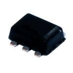
| 产品图片 |
|
| rohs | 符合RoHS无铅 / 符合限制有害物质指令(RoHS)规范要求 |
| 产品系列 | 板上安装温度传感器,Texas Instruments TMP302BDRLT- |
| 数据手册 | |
| 产品型号 | TMP302BDRLT |
| 产品目录页面 | |
| 产品种类 | 板上安装温度传感器 |
| 供应商器件封装 | 6-SOT |
| 关闭 | No Shutdown |
| 其它名称 | 296-25145-6 |
| 准确性 | 2 C |
| 制造商产品页 | http://www.ti.com/general/docs/suppproductinfo.tsp?distId=10&orderablePartNumber=TMP302BDRLT |
| 包装 | 剪切带 (CT) |
| 商标 | Texas Instruments |
| 安装风格 | SMD/SMT |
| 封装 | Reel |
| 封装/外壳 | SOT-563,SOT-666 |
| 封装/箱体 | SOT-553-6 |
| 工厂包装数量 | 250 |
| 感应温度 | 70°C, 75°C, 80°C, 85°C 跳闸点 |
| 数字输出-位数 | None |
| 数字输出-总线接口 | - |
| 最大工作温度 | + 130 C |
| 最小工作温度 | - 55 C |
| 标准包装 | 1 |
| 温度阈值 | Pin Selectable |
| 特性 | 可选跳变点 |
| 电压-电源 | 1.4 V ~ 3.6 V |
| 电源电压-最大 | 3.6 V |
| 电源电压-最小 | 1.4 V |
| 电源电流 | 8 uA |
| 精度 | ±0.2°C |
| 系列 | TMP302B |
| 设备功能 | Single Trip Switch |
| 输出 | 低有效 |
| 输出类型 | 开路漏极 |
| 配置 | Local |


- 商务部:美国ITC正式对集成电路等产品启动337调查
- 曝三星4nm工艺存在良率问题 高通将骁龙8 Gen1或转产台积电
- 太阳诱电将投资9.5亿元在常州建新厂生产MLCC 预计2023年完工
- 英特尔发布欧洲新工厂建设计划 深化IDM 2.0 战略
- 台积电先进制程称霸业界 有大客户加持明年业绩稳了
- 达到5530亿美元!SIA预计今年全球半导体销售额将创下新高
- 英特尔拟将自动驾驶子公司Mobileye上市 估值或超500亿美元
- 三星加码芯片和SET,合并消费电子和移动部门,撤换高东真等 CEO
- 三星电子宣布重大人事变动 还合并消费电子和移动部门
- 海关总署:前11个月进口集成电路产品价值2.52万亿元 增长14.8%


PDF Datasheet 数据手册内容提取
Product Order Technical Tools & Support & Folder Now Documents Software Community TMP302 SBOS488E–JUNE2009–REVISEDDECEMBER2018 TMP302 Easy-to-Use, Low-Power, Low-Supply Temperature Switch in Micropackage 1 Features 3 Description • LowPower:15μA(Maximum) The TMP302 device is a temperature switch in a 1 micropackage (SOT563). The TMP302 offers low • SOT563Package:1.6-mm ×1.6-mm ×0.6mm power (15-μA maximum) and ease-of-use through • Trip-PointAccuracy: ±0.2°C(Typical)From+40°C pin-selectabletrippointsandhysteresis. to+125°C These devices require no additional components for • Pin-SelectableTripPoints operation; they can function independent of • Open-DrainOutput microprocessorsormicrocontrollers. • Pin-SelectableHysteresis:5°Cand10°C The TMP302 is available in several different versions. • LowSupplyVoltageRange:1.4Vto3.6V Foradditionaltrippoints,contactaTIrepresentative. 2 Applications DeviceInformation(1) SELECTABLETRIP • CellPhoneHandsets PARTNUMBER PACKAGE POINTS(ºC)(2) • PortableMediaPlayers TMP302A SOT(6) 50,55,60,65 • ConsumerElectronics TMP302B SOT(6) 70,75,80,85 • Servers TMP302C SOT(6) 90,95,100,105 • Power-SupplySystems TMP302D SOT(6) 110,115,120,125 • DC-DCModules (1) For all available packages, see the orderable addendum at • ThermalMonitoring theendofthedatasheet. (2) Forotheravailabletrippoints,contactaTIrepresentative. • ElectronicProtectionSystems TripThresholdAccuracy 40 35 30 n 25 o ulati 20 p o P 15 10 5 0 098765432101234567890 1.0.0.0.0.0.0.0.0.0. 0.0.0.0.0.0.0.0.0.1. ---------- Accuracy (°C) 1 An IMPORTANT NOTICE at the end of this data sheet addresses availability, warranty, changes, use in safety-critical applications, intellectualpropertymattersandotherimportantdisclaimers.PRODUCTIONDATA.
TMP302 SBOS488E–JUNE2009–REVISEDDECEMBER2018 www.ti.com Table of Contents 1 Features.................................................................. 1 7.4 DeviceFunctionalModes..........................................8 2 Applications........................................................... 1 8 ApplicationandImplementation.......................... 9 3 Description............................................................. 1 8.1 ApplicationInformation..............................................9 4 RevisionHistory..................................................... 2 8.2 TypicalApplication ...................................................9 5 PinConfigurationandFunctions......................... 2 9 PowerSupplyRecommendations...................... 11 6 Specifications......................................................... 4 10 Layout................................................................... 11 6.1 AbsoluteMaximumRatings......................................4 10.1 LayoutGuidelines.................................................11 6.2 ESDRatings..............................................................4 10.2 LayoutExample....................................................11 6.3 RecommendedOperatingConditions.......................4 11 DeviceandDocumentationSupport................. 12 6.4 ThermalInformation..................................................4 11.1 ReceivingNotificationofDocumentationUpdates12 6.5 ElectricalCharacteristics...........................................5 11.2 CommunityResources..........................................12 6.6 TypicalCharacteristics..............................................5 11.3 Trademarks...........................................................12 7 DetailedDescription.............................................. 7 11.4 ElectrostaticDischargeCaution............................12 7.1 Overview...................................................................7 11.5 Glossary................................................................12 7.2 FunctionalBlockDiagram.........................................7 12 Mechanical,Packaging,andOrderable Information........................................................... 12 7.3 FeatureDescription...................................................8 4 Revision History NOTE:Pagenumbersforpreviousrevisionsmaydifferfrompagenumbersinthecurrentversion. ChangesfromRevisionD(October2018)toRevisionE Page • Changedtheinputpinsupplyvoltagemaximumvaluefrom::V +0.5and≤4Vto::V +0.3and≤4V......................... 4 S S ChangesfromRevisionB(December2014)toRevisionC Page • ChangeddevicenamesbysimplifyingfromTMP302A,TMP302B,TMP302C,andTMP302DtoTMP302......................... 1 • Addedplus-minussymboltoMachineModelvalueinESDRatingstable............................................................................. 4 • MovedSpecifiedOperatingTemperatureparameterfromElectricalCharacteristicstabletoRecommended OperatingConditionstable..................................................................................................................................................... 4 • AddedCommunityResourcessection................................................................................................................................. 12 ChangesfromRevisionA(September2009)toRevisionB Page • AddedESDRatingstable,FeatureDescriptionsection,DeviceFunctionalModes,ApplicationandImplementation section,PowerSupplyRecommendationssection,Layoutsection,DeviceandDocumentationSupportsection,and Mechanical,Packaging,andOrderableInformationsection ................................................................................................. 1 5 Pin Configuration and Functions DRLPackage 6-PinSOT TopView TRIPSET0 1 6 TRIPSET1 GND 2 5 VS OUT 3 4 HYSTSET 2 SubmitDocumentationFeedback Copyright©2009–2018,TexasInstrumentsIncorporated ProductFolderLinks:TMP302
TMP302 www.ti.com SBOS488E–JUNE2009–REVISEDDECEMBER2018 PinFunctions PIN TYPE DESCRIPTION NO. NAME 1 TRIPSET0 DigitalInput UsedincombinationwithTRIPSET1toselectthetemperatureatwhichthedevicetrips 2 GND Ground Ground 3 OUT DigitalOutput Opendrain,active-lowoutput 4 HYSTSET DigitalInput Usedtosetamountofthermalhysteresis Power 5 V Powersupply S Supply 6 TRIPSET1 DigitalInput UsedincombinationwithTRIPSET0toselectthetemperatureatwhichthedevicetrips Copyright©2009–2018,TexasInstrumentsIncorporated SubmitDocumentationFeedback 3 ProductFolderLinks:TMP302
TMP302 SBOS488E–JUNE2009–REVISEDDECEMBER2018 www.ti.com 6 Specifications 6.1 Absolute Maximum Ratings overoperatingfree-airtemperaturerange(unlessotherwisenoted)(1) MIN MAX UNIT Supply 4 –0.5 V +0.3 Voltage Inputpin(TRIPSET0,TRIPSET1,HYSTSET) S V and≤4 Outputpin(OUT) –0.5 4 Current Outputpin(OUT) 10 mA Operating –55 130 Temperature Junction 150 °C Storage –60 150 (1) StressesbeyondthoselistedunderAbsoluteMaximumRatingsmaycausepermanentdamagetothedevice.Thesearestressratings only,whichdonotimplyfunctionaloperationofthedeviceattheseoranyotherconditionsbeyondthoseindicatedunderRecommended OperatingConditions.Exposuretoabsolute-maximum-ratedconditionsforextendedperiodsmayaffectdevicereliability. 6.2 ESD Ratings VALUE UNIT Human-bodymodel(HBM),perANSI/ESDA/JEDECJS-001(1) ±2000 V Electrostaticdischarge Charged-devicemodel(CDM),perJEDECspecificationJESD22-C101(2) ±1000 V (ESD) Machinemodel(MM) ±500 (1) JEDECdocumentJEP155statesthat500-VHBMallowssafemanufacturingwithastandardESDcontrolprocess. (2) JEDECdocumentJEP157statesthat250-VCDMallowssafemanufacturingwithastandardESDcontrolprocess. 6.3 Recommended Operating Conditions overoperatingfree-airtemperaturerange(unlessotherwisenoted) MIN NOM MAX UNIT V Powersupplyvoltage 1.4 3.3 3.6 V S R PullupresistorconnectedfromOUTtoV 10 100 kΩ pullup S T Specifiedtemperature –40 125 °C A 6.4 Thermal Information TMP302 THERMALMETRIC(1) DRL(SOT) UNIT 6PINS R Junction-to-ambientthermalresistance 210.3 °C/W θJA R Junction-to-case(top)thermalresistance 105.0 °C/W θJC(top) R Junction-to-boardthermalresistance 87.5 °C/W θJB ψ Junction-to-topcharacterizationparameter 6.1 °C/W JT ψ Junction-to-boardcharacterizationparameter 87.0 °C/W JB (1) Formoreinformationabouttraditionalandnewthermalmetrics,seetheSemiconductorandICPackageThermalMetricsapplication report(SPRA953). 4 SubmitDocumentationFeedback Copyright©2009–2018,TexasInstrumentsIncorporated ProductFolderLinks:TMP302
TMP302 www.ti.com SBOS488E–JUNE2009–REVISEDDECEMBER2018 6.5 Electrical Characteristics AtT =–40°Cto+125°C,andV =1.4to3.6V(unlessotherwisenoted).100%ofallunitsareproductiontestedatT = A S A 25°C;overtemperaturespecificationsarespecifiedbydesign. PARAMETER TESTCONDITIONS MIN TYP MAX UNIT TEMPERATUREMEASUREMENT Trippointaccuracy ±0.2 ±2 °C Trippointaccuracyversus ±0.2 ±0.5 °C/V supply Trippointhysteresis HYSTSET=GND 5 °C HYSTSET=V 10 °C S TEMPERATURETRIPPOINTSET TRIPSET1=GND,TRIPSET0= Default °C GND Temperaturetrippointset TRIPSET1=GND,TRIPSET0=VS Default+5 °C TRIPSET1=V ,TRIPSET0=GND Default+10 °C S TRIPSET1=V ,TRIPSET0=V Default+15 °C S S HYSTERESISSETINPUT V Inputlogiclevelhigh 0.7×V V V IH S S V Inputlogiclevellow –0.5 0.3×V V IL S I Inputcurrent 0<V <3.6V 1 µA I I DIGITALOUTPUT V >2V,I =3mA 0 0.4 V S OL V Outputlogiclevellow OL V <2V,I =3mA 0 0.2×V V S OL S POWERSUPPLY OperatingSupplyRange 1.4 3.6 V T =–40°Cto+125°C 8 15 µA A I QuiescentCurrent Q V =3.3V,T =50°C 7 µA S A 6.6 Typical Characteristics AtT =25°CandV =3.3V,unlessotherwisenoted. A S 2.0 16 V = 3.6 V S 1.5 14 V = 3.3 V S 1.0 A) 12 V = 1.4 V acy (C)° 0.5 urrent (µ 10 S ur 0 C 8 cc nt TripA --01..50 Quiesce 64 -1.5 2 -2.0 0 40 50 60 70 80 90 100 110 120 130 -75 -50 -25 0 25 50 75 100 125 150 Temperature (°C) Temperature (°C) 30typicalunits Figure1.TripAccuracyErrorvsTemperature Figure2.QuiescentCurrentvsTemperature Copyright©2009–2018,TexasInstrumentsIncorporated SubmitDocumentationFeedback 5 ProductFolderLinks:TMP302
TMP302 SBOS488E–JUNE2009–REVISEDDECEMBER2018 www.ti.com Typical Characteristics (continued) AtT =25°CandV =3.3V,unlessotherwisenoted. A S 120 100 90 100 80 C) 80 C) 70 e (° e (° 60 ur ur at 60 at 50 er er p p 40 m m Te 40 Te 30 20 20 10 0 0 0 5 10 15 20 25 30 0 20 40 60 80 100 120 140 160 180 200 Time (s) Time (s) Figure3.TemperatureStepResponseinPerfluorinated Figure4.ThermalStepResponseinAirat100°CvsTime Fluidat100°CvsTime 40 400 35 350 V) 30 w (m 300 n 25 Lo 250 opulatio 20 c Level 200 P 15 ogi 150 L 10 put 100 ut 5 O 50 0 0 1.00.90.80.70.60.50.40.30.20.100.10.20.30.40.50.60.70.80.91.0 -75 -50 -25 0 25 50 75 100 125 150 ---------- Accuracy (°C) Temperature (°C) V =1.4V I =2mA S OL Figure5.TripThresholdAccuracy Figure6.OutputLogic-LevelLowVOLvsTemperature OUT OUT VS VS v) v) di di V/ V/ 2 2 e ( e ( g g a a Volt Volt Time (8 µs/div) Time (10 ms/div) TMP302A,T =55°C TRIPSET1=TRIPSET0=GND A Figure7.Power-UpandPower-DownResponse Figure8.Power-Up,Trip,andPower-DownResponse 6 SubmitDocumentationFeedback Copyright©2009–2018,TexasInstrumentsIncorporated ProductFolderLinks:TMP302
TMP302 www.ti.com SBOS488E–JUNE2009–REVISEDDECEMBER2018 7 Detailed Description 7.1 Overview The TMP302 temperature switch is optimal for ultra low-power applications that require accurate trip thresholds. A temperature switch is a device that issues an alert response when a temperature threshold is reached or exceeded. The trip thresholds are programmable to four different settings using the TRIPSET1 and TRIPSET0 pins.Table1liststhepinsettingsversustrippoints. Table1.TripPointversusTRIPSET1andTRIPSET0 TRIPSET1 TRIPSET0 TMP302A TMP302B TMP302C TMP302D GND GND 50°C 70°C 90°C 110°C GND VS 55°C 75°C 95°C 115°C VS GND 60°C 80°C 100°C 120°C VS VS 65°C 85°C 105°C 125°C 7.2 Functional Block Diagram VS Bias TRIPSET0 Temperature Threshold and Hysteresis TRIPSET1 HYSTSET Comparator Alert OUT Temperature Sensor GROUND Copyright©2009–2018,TexasInstrumentsIncorporated SubmitDocumentationFeedback 7 ProductFolderLinks:TMP302
TMP302 SBOS488E–JUNE2009–REVISEDDECEMBER2018 www.ti.com 7.3 Feature Description 7.3.1 HYSTSET Ifthetemperaturetripthresholdiscrossed,theopen-drain,activelowoutput(OUT)goeslowanddoesnotreturn to the original high state (that is, V ) until the temperature returns to a value within a hysteresis window set by S the HYSTSET pin. The HYSTSET pin allows the user to choose between a 5°C and a 10°C hysteresis window. Table2liststhehysteresiswindowthatcorrespondstotheHYSTSETsetting. Table2.HYSTSETWindow HYSTSET THRESHOLDHYSTERESIS GND 5°C V 10°C S Forthespecificcaseofthedevice,iftheHYSTSETpinissetto10°C(thatis,connectedtoV )andthedeviceis S configured with a 60°C trip point (TRIPSET1 = V , TRIPSET0 = GND), when this threshold is exceeded the S outputdoesnotreturntotheoriginalhighstateuntilitreaches50°C.ThiscaseismoreclearlyshowninFigure9. OUT V S 50°C 60°C T (TRIP) Figure9. TMP302A:HYSTSET=V ,TRIPSET1=V ,TRIPSET0=GND S S 7.4 Device Functional Modes The TMP302 family of devices has a single functional mode. Normal operation for the TMP302 family of devices occurs when the power-supply voltage applied between the V pin and GND is within the specified operating S range of 1.4 to 3.6 V. The temperature threshold is selected by connecting the TRIPSET0 and TRIPSET1 pins to either the GND or V pins (see Table 1). Hysteresis is selected by connecting the HYSTSET pin to either the S GND or V pins (see Table 2). The output pin, OUT, remains high when the temperature is below the selected S temperature threshold. The OUT pin remains low when the temperature is at or above the selected temperature threshold. The OUT pin returns from a low state back to the high state based upon the amount of selected hysteresis(seetheHYSTSETsection). 8 SubmitDocumentationFeedback Copyright©2009–2018,TexasInstrumentsIncorporated ProductFolderLinks:TMP302
TMP302 www.ti.com SBOS488E–JUNE2009–REVISEDDECEMBER2018 8 Application and Implementation NOTE Information in the following applications sections is not part of the TI component specification, and TI does not warrant its accuracy or completeness. TI’s customers are responsible for determining suitability of components for their purposes. Customers should validateandtesttheirdesignimplementationtoconfirmsystemfunctionality. 8.1 Application Information 8.1.1 ConfiguringtheTMP302 The TMP302 family of devices is simple to configure. The only external components that the device requires are a bypass capacitor and pullup resistor. Power-supply bypassing is strongly recommended. Use a 0.1-µF capacitor placed as close as possible to the supply pin. To minimize the internal power dissipation of the TMP302 family of devices, use a pullup resistor value greater than 10 kΩ from the OUT pin to the V pin. Refer S to Table 1 for trip-point temperature configuration. The TRIPSET pins can be toggled dynamically; however, the voltage of these pins must not exceed V . To ensure a proper logic high, the voltage must not drop below 0.7 V S ×V . S 8.2 Typical Application Figure 10 shows the typical circuit configuration for the TMP302 family of devices. The TMP302 family of devices is configured for the default temperature threshold by connecting the TRIPSET0 and TRIPSET1 pins directly to ground. Connecting the HYSTSET pin to ground configures the device for 5°C of hysteresis. Place a 10-kΩ pullup resistor between the OUT and V pins. Place a 0.1-µF bypass capacitor between the V pin and ground, S S closetotheTMP302device. TMP302 TRIPSET0 TRIPSET1 10 k(cid:13) GND VS VS OUTPUT OUT HYSTSET 0.1 µF 1.4 V to 3.6 V Figure10. TMP302TypicalApplicationSchematic Figure 11 shows the most generic implementation of the TMP302 family of devices. Switches are shown connecting the TMPSET0, TMPSET1 and HYSTSET pins to either V or ground. The use of switches is not S strictly required; the switches are shown only to illustrate the various pin connection combinations. In practice, connecting the TMPSET0, TMPSET1 and HYSTSET pins to ground or directly to the V pin is sufficient and S minimizes space and cost. If additional flexibility is desired, connections from the TMPSET0, TMPSET1 and HYSTSET pins can be made through 0-Ω resistors which can be either populated or not populated depending uponthedesiredconnection. Copyright©2009–2018,TexasInstrumentsIncorporated SubmitDocumentationFeedback 9 ProductFolderLinks:TMP302
TMP302 SBOS488E–JUNE2009–REVISEDDECEMBER2018 www.ti.com Typical Application (continued) TMP302 10 k(cid:13) TRIPSET0 TRIPSET1 GND VS OUTPUT OUT HYSTSET VS 0.1 µF 1.4 V to 3.6 V Figure11. TMP302GenericApplicationSchematic 8.2.1 DesignRequirements Designing with the TMP302 family of devices is simple. The TMP302 family of devices is a temperature switch commonly used to signal a microprocessor in the event of an over temperature condition. The temperature at which the TMP302 family of devices issues an active low alert is determined by the configuration of the TRIPSET0 and TRIPSET1 pins. These two pins are digital inputs and must be tied either high or low, according to Table 1. The TMP302 family of devices issues an active low alert when the temperature threshold is exceeded. The device has built-in hysteresis to avoid the device from signaling the microprocessor as soon as the temperature drops below the temperature threshold. The amount of hysteresis is determined by the HYSTSETpin.Thispinisadigitalinputandmustbetiedeitherhighorlow,accordingtoTable2. SeeFigure10andFigure11fortypicalcircuitconfigurations. 8.2.2 DetailedDesignProcedure Determine the threshold temperature and hysteresis required for the application. Connect the TMPSET0, TMPSET1,andHYSTSETpinsaccordingtothedesignrequirements.RefertoTable1 andTable2.Usea10-kΩ pullup resistor from the OUT pin to the V pin. To minimize power, a larger-value pullup resistor can be used but S must not exceed 100 kΩ. Place a 0.1-µF bypass capacitor close to the TMP302 device to reduce noise coupled fromthepowersupply. 8.2.3 ApplicationCurves Figure 12 and Figure 13 show the TMP302A power-on response with the ambient temperature less than 50°C and greater than 50°C respectively. The TMP302A was configured with trip point set to 50°C. The TMP302B, TMP302C, and TMP302D devices behave similarly with regards to power on response with T below or above A thetrippoint.Notethatthe OUT signaltypicallyrequires35msfollowingpowerontobecomevalid. 10 SubmitDocumentationFeedback Copyright©2009–2018,TexasInstrumentsIncorporated ProductFolderLinks:TMP302
TMP302 www.ti.com SBOS488E–JUNE2009–REVISEDDECEMBER2018 Typical Application (continued) OUT OUT VS VS v) v) di di V/ V/ 2 2 e ( e ( g g a a olt olt V V Time (5 µs/div) Time (10 ms/div) Figure12.TMP302APower-OnResponse, Figure13.TMP302APower-OnResponse, T Lessthan50°C T Greaterthan50°C A A 9 Power Supply Recommendations The TMP302 family of devices is designed to operate from a single power supply within the range 1.4 V and 3.6 V. No specific power supply sequencing with respect to any of the input or output pins is required. The TMP302 familyofdevicesisfullyfunctionalwithin35msofthevoltageattheV pinreachingorexceeding1.4V. S 10 Layout 10.1 Layout Guidelines Place the power supply bypass capacitor as close as possible to the V and GND pins. The recommended value S forthisbypasscapacitoris0.1-µF.Additionalbypasscapacitancecanbeaddedtocompensatefornoisyorhigh- impedance power supplies. Place a 10-kΩ pullup resistor from the open drain OUT pin to the power supply pin V . S 10.2 Layout Example VIA to Power Ground Plane 0.1 µF TRIPSET0 TRIPSET1 GND VS Supply Voltage OUT HYSTSET 10 k(cid:13) Ground Plane for Thermal Coupling to Heat Source Output Heat Source Figure14. LayoutExample Copyright©2009–2018,TexasInstrumentsIncorporated SubmitDocumentationFeedback 11 ProductFolderLinks:TMP302
TMP302 SBOS488E–JUNE2009–REVISEDDECEMBER2018 www.ti.com 11 Device and Documentation Support 11.1 Receiving Notification of Documentation Updates To receive notification of documentation updates, navigate to the device product folder on ti.com. In the upper right corner, click on Alert me to register and receive a weekly digest of any product information that has changed.Forchangedetails,reviewtherevisionhistoryincludedinanyreviseddocument. 11.2 Community Resources The following links connect to TI community resources. Linked contents are provided "AS IS" by the respective contributors. They do not constitute TI specifications and do not necessarily reflect TI's views; see TI's Terms of Use. TIE2E™OnlineCommunity TI'sEngineer-to-Engineer(E2E)Community.Createdtofostercollaboration amongengineers.Ate2e.ti.com,youcanaskquestions,shareknowledge,exploreideasandhelp solveproblemswithfellowengineers. DesignSupport TI'sDesignSupport QuicklyfindhelpfulE2Eforumsalongwithdesignsupporttoolsand contactinformationfortechnicalsupport. 11.3 Trademarks E2EisatrademarkofTexasInstruments. Allothertrademarksarethepropertyoftheirrespectiveowners. 11.4 Electrostatic Discharge Caution This integrated circuit can be damaged by ESD. Texas Instruments recommends that all integrated circuits be handled with appropriateprecautions.Failuretoobserveproperhandlingandinstallationprocedurescancausedamage. ESDdamagecanrangefromsubtleperformancedegradationtocompletedevicefailure.Precisionintegratedcircuitsmaybemore susceptibletodamagebecauseverysmallparametricchangescouldcausethedevicenottomeetitspublishedspecifications. 11.5 Glossary SLYZ022—TIGlossary. Thisglossarylistsandexplainsterms,acronyms,anddefinitions. 12 Mechanical, Packaging, and Orderable Information The following pages include mechanical, packaging, and orderable information. This information is the most current data available for the designated devices. This data is subject to change without notice and revision of thisdocument.Forbrowser-basedversionsofthisdatasheet,refertotheleft-handnavigation. 12 SubmitDocumentationFeedback Copyright©2009–2018,TexasInstrumentsIncorporated ProductFolderLinks:TMP302
PACKAGE OPTION ADDENDUM www.ti.com 22-Dec-2018 PACKAGING INFORMATION Orderable Device Status Package Type Package Pins Package Eco Plan Lead/Ball Finish MSL Peak Temp Op Temp (°C) Device Marking Samples (1) Drawing Qty (2) (6) (3) (4/5) TMP302ADRLR ACTIVE SOT-5X3 DRL 6 4000 Green (RoHS CU NIPDAU | Level-1-260C-UNLIM -40 to 125 OCP & no Sb/Br) CU NIPDAUAG TMP302ADRLT ACTIVE SOT-5X3 DRL 6 250 Green (RoHS CU NIPDAU | Level-1-260C-UNLIM -40 to 125 OCP & no Sb/Br) CU NIPDAUAG TMP302BDRLR ACTIVE SOT-5X3 DRL 6 4000 Green (RoHS CU NIPDAU | Level-1-260C-UNLIM -40 to 125 OCT & no Sb/Br) CU NIPDAUAG TMP302BDRLT ACTIVE SOT-5X3 DRL 6 250 Green (RoHS CU NIPDAU | Level-1-260C-UNLIM -40 to 125 OCT & no Sb/Br) CU NIPDAUAG TMP302CDRLR ACTIVE SOT-5X3 DRL 6 4000 Green (RoHS CU NIPDAU | Level-1-260C-UNLIM -40 to 125 OCR & no Sb/Br) CU NIPDAUAG TMP302CDRLT ACTIVE SOT-5X3 DRL 6 250 Green (RoHS CU NIPDAU | Level-1-260C-UNLIM -40 to 125 OCR & no Sb/Br) CU NIPDAUAG TMP302DDRLR ACTIVE SOT-5X3 DRL 6 4000 Green (RoHS CU NIPDAU | Level-1-260C-UNLIM -40 to 125 OCS & no Sb/Br) CU NIPDAUAG TMP302DDRLT ACTIVE SOT-5X3 DRL 6 250 Green (RoHS CU NIPDAU | Level-1-260C-UNLIM -40 to 125 OCS & no Sb/Br) CU NIPDAUAG (1) The marketing status values are defined as follows: ACTIVE: Product device recommended for new designs. LIFEBUY: TI has announced that the device will be discontinued, and a lifetime-buy period is in effect. NRND: Not recommended for new designs. Device is in production to support existing customers, but TI does not recommend using this part in a new design. PREVIEW: Device has been announced but is not in production. Samples may or may not be available. OBSOLETE: TI has discontinued the production of the device. (2) RoHS: TI defines "RoHS" to mean semiconductor products that are compliant with the current EU RoHS requirements for all 10 RoHS substances, including the requirement that RoHS substance do not exceed 0.1% by weight in homogeneous materials. Where designed to be soldered at high temperatures, "RoHS" products are suitable for use in specified lead-free processes. TI may reference these types of products as "Pb-Free". RoHS Exempt: TI defines "RoHS Exempt" to mean products that contain lead but are compliant with EU RoHS pursuant to a specific EU RoHS exemption. Green: TI defines "Green" to mean the content of Chlorine (Cl) and Bromine (Br) based flame retardants meet JS709B low halogen requirements of <=1000ppm threshold. Antimony trioxide based flame retardants must also meet the <=1000ppm threshold requirement. (3) MSL, Peak Temp. - The Moisture Sensitivity Level rating according to the JEDEC industry standard classifications, and peak solder temperature. (4) There may be additional marking, which relates to the logo, the lot trace code information, or the environmental category on the device. Addendum-Page 1
PACKAGE OPTION ADDENDUM www.ti.com 22-Dec-2018 (5) Multiple Device Markings will be inside parentheses. Only one Device Marking contained in parentheses and separated by a "~" will appear on a device. If a line is indented then it is a continuation of the previous line and the two combined represent the entire Device Marking for that device. (6) Lead/Ball Finish - Orderable Devices may have multiple material finish options. Finish options are separated by a vertical ruled line. Lead/Ball Finish values may wrap to two lines if the finish value exceeds the maximum column width. Important Information and Disclaimer:The information provided on this page represents TI's knowledge and belief as of the date that it is provided. TI bases its knowledge and belief on information provided by third parties, and makes no representation or warranty as to the accuracy of such information. Efforts are underway to better integrate information from third parties. TI has taken and continues to take reasonable steps to provide representative and accurate information but may not have conducted destructive testing or chemical analysis on incoming materials and chemicals. TI and TI suppliers consider certain information to be proprietary, and thus CAS numbers and other limited information may not be available for release. In no event shall TI's liability arising out of such information exceed the total purchase price of the TI part(s) at issue in this document sold by TI to Customer on an annual basis. OTHER QUALIFIED VERSIONS OF TMP302 : •Automotive: TMP302-Q1 NOTE: Qualified Version Definitions: •Automotive - Q100 devices qualified for high-reliability automotive applications targeting zero defects Addendum-Page 2
PACKAGE MATERIALS INFORMATION www.ti.com 10-Nov-2018 TAPE AND REEL INFORMATION *Alldimensionsarenominal Device Package Package Pins SPQ Reel Reel A0 B0 K0 P1 W Pin1 Type Drawing Diameter Width (mm) (mm) (mm) (mm) (mm) Quadrant (mm) W1(mm) TMP302ADRLR SOT-5X3 DRL 6 4000 180.0 8.4 1.98 1.78 0.69 4.0 8.0 Q3 TMP302ADRLT SOT-5X3 DRL 6 250 180.0 8.4 1.98 1.78 0.69 4.0 8.0 Q3 TMP302BDRLR SOT-5X3 DRL 6 4000 180.0 9.5 1.78 1.78 0.69 4.0 8.0 Q3 TMP302BDRLR SOT-5X3 DRL 6 4000 180.0 8.4 1.98 1.78 0.69 4.0 8.0 Q3 TMP302BDRLT SOT-5X3 DRL 6 250 180.0 8.4 1.98 1.78 0.69 4.0 8.0 Q3 TMP302BDRLT SOT-5X3 DRL 6 250 180.0 9.5 1.78 1.78 0.69 4.0 8.0 Q3 TMP302CDRLR SOT-5X3 DRL 6 4000 180.0 8.4 1.98 1.78 0.69 4.0 8.0 Q3 TMP302CDRLR SOT-5X3 DRL 6 4000 180.0 9.5 1.78 1.78 0.69 4.0 8.0 Q3 TMP302CDRLT SOT-5X3 DRL 6 250 180.0 9.5 1.78 1.78 0.69 4.0 8.0 Q3 TMP302DDRLR SOT-5X3 DRL 6 4000 180.0 8.4 1.98 1.78 0.69 4.0 8.0 Q3 TMP302DDRLR SOT-5X3 DRL 6 4000 180.0 9.5 1.78 1.78 0.69 4.0 8.0 Q3 TMP302DDRLT SOT-5X3 DRL 6 250 180.0 9.5 1.78 1.78 0.69 4.0 8.0 Q3 TMP302DDRLT SOT-5X3 DRL 6 250 180.0 8.4 1.98 1.78 0.69 4.0 8.0 Q3 PackMaterials-Page1
PACKAGE MATERIALS INFORMATION www.ti.com 10-Nov-2018 *Alldimensionsarenominal Device PackageType PackageDrawing Pins SPQ Length(mm) Width(mm) Height(mm) TMP302ADRLR SOT-5X3 DRL 6 4000 202.0 201.0 28.0 TMP302ADRLT SOT-5X3 DRL 6 250 202.0 201.0 28.0 TMP302BDRLR SOT-5X3 DRL 6 4000 184.0 184.0 19.0 TMP302BDRLR SOT-5X3 DRL 6 4000 202.0 201.0 28.0 TMP302BDRLT SOT-5X3 DRL 6 250 202.0 201.0 28.0 TMP302BDRLT SOT-5X3 DRL 6 250 184.0 184.0 19.0 TMP302CDRLR SOT-5X3 DRL 6 4000 202.0 201.0 28.0 TMP302CDRLR SOT-5X3 DRL 6 4000 184.0 184.0 19.0 TMP302CDRLT SOT-5X3 DRL 6 250 184.0 184.0 19.0 TMP302DDRLR SOT-5X3 DRL 6 4000 202.0 201.0 28.0 TMP302DDRLR SOT-5X3 DRL 6 4000 184.0 184.0 19.0 TMP302DDRLT SOT-5X3 DRL 6 250 184.0 184.0 19.0 TMP302DDRLT SOT-5X3 DRL 6 250 202.0 201.0 28.0 PackMaterials-Page2
PACKAGE OUTLINE DRL0006A SOT - 0.6 mm max height SCALE 8.000 PLASTIC SMALL OUTLINE 1.7 1.5 PIN 1 A ID AREA 1 6 4X 0.5 1.7 1.5 2X 1 NOTE 3 4 3 B 11..31 6X 00..31 00..0050 TYP 0.6 MAX C SEATING PLANE 0.18 6X 0.08 SYMM 0.05 C SYMM 0.27 6X 0.15 0.1 C A B 0.4 6X 0.2 0.05 4223266/A 09/2016 NOTES: 1. All linear dimensions are in millimeters. Any dimensions in parenthesis are for reference only. Dimensioning and tolerancing per ASME Y14.5M. 2. This drawing is subject to change without notice. 3. This dimension does not include mold flash, protrusions, or gate burrs. Mold flash, protrusions, or gate burrs shall not exceed 0.15 mm per side. www.ti.com
EXAMPLE BOARD LAYOUT DRL0006A SOT - 0.6 mm max height PLASTIC SMALL OUTLINE 6X (0.67) SYMM 1 6X (0.3) 6 SYMM 4X (0.5) 4 3 (R0.05) TYP (1.48) LAND PATTERN EXAMPLE SCALE:30X 0.05 MAX 0.05 MIN AROUND AROUND SOLDER MASK METAL METAL UNDER SOLDER MASK OPENING SOLDER MASK OPENING NON SOLDER MASK SOLDER MASK DEFINED DEFINED (PREFERRED) SOLDERMASK DETAILS 4223266/A 09/2016 NOTES: (continued) 4. Publication IPC-7351 may have alternate designs. 5. Solder mask tolerances between and around signal pads can vary based on board fabrication site. www.ti.com
EXAMPLE STENCIL DESIGN DRL0006A SOT - 0.6 mm max height PLASTIC SMALL OUTLINE 6X (0.67) SYMM 1 6X (0.3) 6 SYMM 4X (0.5) 4 3 (R0.05) TYP (1.48) SOLDER PASTE EXAMPLE BASED ON 0.1 mm THICK STENCIL SCALE:30X 4223266/A 09/2016 NOTES: (continued) 6. Laser cutting apertures with trapezoidal walls and rounded corners may offer better paste release. IPC-7525 may have alternate design recommendations. 7. Board assembly site may have different recommendations for stencil design. www.ti.com
IMPORTANTNOTICEANDDISCLAIMER TIPROVIDESTECHNICALANDRELIABILITYDATA(INCLUDINGDATASHEETS),DESIGNRESOURCES(INCLUDINGREFERENCE DESIGNS),APPLICATIONOROTHERDESIGNADVICE,WEBTOOLS,SAFETYINFORMATION,ANDOTHERRESOURCES“ASIS” ANDWITHALLFAULTS,ANDDISCLAIMSALLWARRANTIES,EXPRESSANDIMPLIED,INCLUDINGWITHOUTLIMITATIONANY IMPLIEDWARRANTIESOFMERCHANTABILITY,FITNESSFORAPARTICULARPURPOSEORNON-INFRINGEMENTOFTHIRD PARTYINTELLECTUALPROPERTYRIGHTS. TheseresourcesareintendedforskilleddevelopersdesigningwithTIproducts.Youaresolelyresponsiblefor(1)selectingtheappropriate TIproductsforyourapplication,(2)designing,validatingandtestingyourapplication,and(3)ensuringyourapplicationmeetsapplicable standards,andanyothersafety,security,orotherrequirements.Theseresourcesaresubjecttochangewithoutnotice.TIgrantsyou permissiontousetheseresourcesonlyfordevelopmentofanapplicationthatusestheTIproductsdescribedintheresource.Other reproductionanddisplayoftheseresourcesisprohibited.NolicenseisgrantedtoanyotherTIintellectualpropertyrightortoanythird partyintellectualpropertyright.TIdisclaimsresponsibilityfor,andyouwillfullyindemnifyTIanditsrepresentativesagainst,anyclaims, damages,costs,losses,andliabilitiesarisingoutofyouruseoftheseresources. TI’sproductsareprovidedsubjecttoTI’sTermsofSale(www.ti.com/legal/termsofsale.html)orotherapplicabletermsavailableeitheron ti.comorprovidedinconjunctionwithsuchTIproducts.TI’sprovisionoftheseresourcesdoesnotexpandorotherwisealterTI’sapplicable warrantiesorwarrantydisclaimersforTIproducts. MailingAddress:TexasInstruments,PostOfficeBox655303,Dallas,Texas75265 Copyright©2019,TexasInstrumentsIncorporated