 Datasheet下载
- 型号: TMDS361BPAG
- 制造商: Texas Instruments
- 库位|库存: xxxx|xxxx
- 要求:
| 数量阶梯 | 香港交货 | 国内含税 |
| +xxxx | $xxxx | ¥xxxx |
查看当月历史价格
查看今年历史价格
TMDS361BPAG产品简介:
ICGOO电子元器件商城为您提供TMDS361BPAG由Texas Instruments设计生产,在icgoo商城现货销售,并且可以通过原厂、代理商等渠道进行代购。 TMDS361BPAG价格参考¥14.20-¥29.10。Texas InstrumentsTMDS361BPAG封装/规格:线性 - 视频处理, 。您可以下载TMDS361BPAG参考资料、Datasheet数据手册功能说明书,资料中有TMDS361BPAG 详细功能的应用电路图电压和使用方法及教程。
TMDS361BPAG 是由 Texas Instruments(德州仪器)生产的一款线性视频处理芯片,属于 TMDS(Transition Minimized Differential Signaling,最小化传输差分信号)系列。该型号主要应用于高清视频信号的传输和处理领域,具体应用场景如下:

1. 显示器接口:
   TMDS361BPAG 常用于液晶显示器(LCD)、投影仪和其他显示设备中,作为 HDMI 或 DVI 接口的核心组件之一,负责将数字视频信号从源设备(如电脑、机顶盒或游戏机)传输到显示设备。

2. 视频分配与切换:
   在多路视频信号切换器或分配器中,该芯片可以实现信号的高效传输和处理,确保视频质量不因切换或分配而受损。

3. 嵌入式系统中的视频处理:
   在工业控制、医疗设备或车载娱乐系统中,TMDS361BPAG 能够支持高分辨率视频信号的稳定传输,满足对可靠性和性能要求较高的应用需求。

4. 高清电视(HDTV):
   该芯片广泛应用于高清电视中,用于处理来自外部设备的数字视频信号,支持高质量的图像显示。

5. 视频采集卡与转换器:
   在视频采集卡或信号转换器(如 VGA 到 HDMI 转换器)中,TMDS361BPAG 能够实现不同接口之间的信号转换,同时保持低延迟和高画质。

 技术特点:
- 支持高达 1.65 Gbps 的数据速率,适用于全高清(1080p)及更高分辨率的视频传输。
- 内置均衡器和预加重功能,优化长距离信号传输的质量。
- 提供低功耗设计,适合便携式或节能型设备。

总之,TMDS361BPAG 主要用于需要高性能、低噪声和稳定传输的数字视频信号处理场景,是现代显示技术和多媒体设备中不可或缺的关键组件之一。
| 参数 | 数值 |
| 产品目录 | 集成电路 (IC)半导体 |
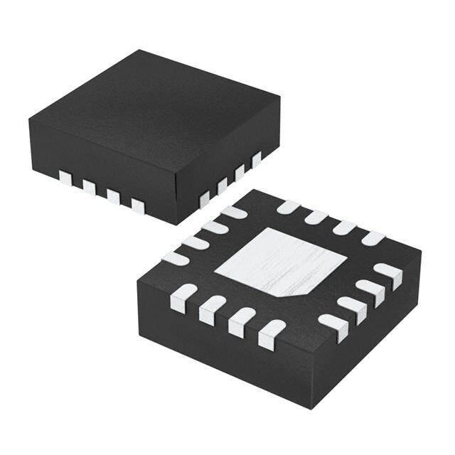
| 描述 | IC SWITCH DVI/HDMI 3:1 64-TQFP视频开关 IC 3 to 1 HDMI switch |
| 产品分类 | |
| 品牌 | Texas Instruments |
| 产品手册 | |
| 产品图片 |
|
| rohs | 符合RoHS无铅 / 符合限制有害物质指令(RoHS)规范要求 |
| 产品系列 | 开关 IC,视频开关 IC,Texas Instruments TMDS361BPAG- |
| 数据手册 | |
| 产品型号 | TMDS361BPAG |
| 产品目录页面 | |
| 产品种类 | 视频开关 IC |
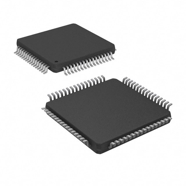
| 供应商器件封装 | 64-TQFP(10x10) |
| 其它名称 | 296-25278 |
| 包装 | 托盘 |
| 商标 | Texas Instruments |
| 安装类型 | 表面贴装 |
| 安装风格 | SMD/SMT |
| 封装 | Tray |
| 封装/外壳 | 64-TQFP |
| 封装/箱体 | TQFP-64 |
| 工作频率 | 100 kHz |
| 工厂包装数量 | 160 |
| 应用 | HDTV |
| 开关数量 | 3 Switch |
| 最大工作温度 | + 70 C |
| 最小工作温度 | 0 C |
| 标准包装 | 160 |
| 电源电压-最大 | 3.6 V |
| 电源电压-最小 | - 0.3 V |
| 电源电流 | 216 mA |
| 类型 | HDMI/DVI 开关 |
| 系列 | TMDS361B |


- 商务部:美国ITC正式对集成电路等产品启动337调查
- 曝三星4nm工艺存在良率问题 高通将骁龙8 Gen1或转产台积电
- 太阳诱电将投资9.5亿元在常州建新厂生产MLCC 预计2023年完工
- 英特尔发布欧洲新工厂建设计划 深化IDM 2.0 战略
- 台积电先进制程称霸业界 有大客户加持明年业绩稳了
- 达到5530亿美元!SIA预计今年全球半导体销售额将创下新高
- 英特尔拟将自动驾驶子公司Mobileye上市 估值或超500亿美元
- 三星加码芯片和SET,合并消费电子和移动部门,撤换高东真等 CEO
- 三星电子宣布重大人事变动 还合并消费电子和移动部门
- 海关总署:前11个月进口集成电路产品价值2.52万亿元 增长14.8%


PDF Datasheet 数据手册内容提取
TMDS361B www.ti.com SLLS988A–SEPTEMBER2009–REVISEDJULY2011 Three-Port HDMI Switch CheckforSamples:TMDS361B FEATURES • 3.3-VoltPowerSupply 1 • 3:1Sink-sideswitchSupportingDVIAbove • TemperatureRange:0°Cto70°C 2 1920×1200andHDMIHDTVResolutionsupto • 64-PinTQFPPackage:Pin-CompatibleWith 1080pWith16-BitColorDepth TMDS351 • DesignedforSignalingRatesupto3Gbps • RobustTMDSReceiveStageThatCanWork • SupportsHDMI1.3aSpecification WithNon-CompliantInputCommon-Mode HDMISignal • AdaptiveEqualizationoninputstosupportup to20-mHDMICableat2.25Gbpsfor1080p APPLICATIONS 12-BitColorDepth • TMDSInputClock-DetectCircuit • High-DefinitionDigitalTV • DDCRepeaterFunction – LCD • <2-mWLow-PowerMode – Plasma • LocalI2CorGPIOConfigurable – DLP® • EnhancedESD.HBM:10kVonAllInput TMDS,DDCI2C,HPDPins DESCRIPTION The TMDS361B is a three-port digital video interface (DVI) or high-definition multimedia interface (HDMI) switch that allows up to three DVI or HDMI ports to be switched to a single display terminal. Four TMDS channels, one hot-plug detector, and a digital display control (DDC) interface are supported on each port. Each TMDS channel supports signaling rates up to 3 Gbps to allow 1080p resolution in 16-bit color depth. TMDS361B is not intended forsourcesideapplicationssuchasexternalswitchboxes. The TMDS361B provides an adaptive equalizer for different ranges of cable lengths. The equalizer automatically compensates for intersymbol interference [ISI] loss of an HDMI/DVI cable for up to 20 dB at 3 Gbps. (see Figure15). TYPICAL APPLICATION DigitalTV Digital Camcorder BRTN TV1 Game Machine TMDS361 169 PALplus DVD Player or DVR M0124-01 1 Pleasebeawarethatanimportantnoticeconcerningavailability,standardwarranty,anduseincriticalapplicationsofTexas Instrumentssemiconductorproductsanddisclaimerstheretoappearsattheendofthisdatasheet. DLPisaregisteredtrademarkofTexasInstruments. 2 PRODUCTIONDATAinformationiscurrentasofpublicationdate. Copyright©2009–2011,TexasInstrumentsIncorporated Products conform to specifications per the terms of the Texas Instruments standard warranty. Production processing does not necessarilyincludetestingofallparameters.
TMDS361B SLLS988A–SEPTEMBER2009–REVISEDJULY2011 www.ti.com Thesedeviceshavelimitedbuilt-inESDprotection.Theleadsshouldbeshortedtogetherorthedeviceplacedinconductivefoam duringstorageorhandlingtopreventelectrostaticdamagetotheMOSgates. DESCRIPTION (CONTINUED) When any of the input ports are selected, the integrated terminations (50-Ω termination resistors pulled up to VCC) are switched on for the TMDS clock channel, the TMDS clock-detection circuit is enabled, and the DDC repeater is enabled. After a valid TMDS clock is detected, the integrated termination resistors for the data lines are enabled, and the output TMDS lines are enabled. When an input port is not selected, the integrated terminations are switched off, the TMDS receivers are disabled, and the DDC repeater is disabled. Clock-detection circuitry provides an automatic power-management feature, because if no valid TMDS clock is detected, the terminations on the input TMDS data lines are disconnected and the TMDS outputs are placed in a high-impedancestate. The TMDS361B is designed to be controlled via a local I2C interface or GPIO interface based on the status of the I2C_SEL pin. The local I2C interface in TMDS361B is a slave-only I2C interface. (See the I2C INTERFACE NOTESsection.) I2C Mode: When the I2C_SEL pin is set low, the device is in I2C mode. With local I2C, the interface port status can be read and the advanced configurations of the device such as TMDS output edge rate control, DDC I2C buffer output-voltage-select (OVS) settings (See the DDC I2C Function Description for detailed description on DDC I2C buffer description and OVS description), device power management, TMDS clock-detect feature, and TMDSinput-portselectioncanbeset.SeeTable8throughTable11. GPIO mode: When the I2C_SEL pin is set high, the device is in GPIO control mode. The port selection is controlled with source selectors, S1 and S2. The power-saving mode is controlled through the LP pin. In GPIO mode, the default TMDS output edge rate that is the fastest setting of rise and fall time is set, and the default DDC I2C buffer OVS setting (OVS3) is set. See Table 8 and the DDC I2C Function Description for a detailed descriptionoftheDDCI2Cbuffer. Following are some of the key features (advantages) that TMDS361B provides to the overall sink-side system (HDTV). • 3×1switchthatsupportsTMDSdataratesupto3Gbpsonallthreeinputports • ESD: Built-in support for high ESD protection (up to 10 kV on the HDMI source side). The HDMI source-side pins on the TMDS361B are connected via the HDMI/DVI exterior connectors and cable to the HDMI/DVI sources (e.g., DVD player). In TV applications, it can be expected that the source side may be subjected to higherESDstressescomparedtothesinksidethatisconnectedinternallytotheHDMIreceiver. • Adaptive equalization: The built-in adaptive equalization support compensates for intersymbol interference [ISI] loss of up to 20 dB, which represents a typical 20-m HDMI/DVI cable at 3 Gbps. Adaptive equalization adjuststheequalizationgainautomatically,basedonthecablelengthandtheincomingTMDSdatarate. • TMDSclock-detectcircuitry:Thisfeatureprovidesanautomaticpower-managementfeatureandalsoensures that the TMDS output port is turned on only if there is a valid TMDS input signal. TMDS clock-detect feature can be bypassed in I2C mode; see Table 10 and Table 11. It is recommended to enable the TMDS clock-detect circuitry during normal operation. However, for HDMI compliance testing (TMDS termination-voltage test), the clock-detect feature should be disabled by using the I2C mode control. If the customer requires passing the TMDS termination-voltage test in GPIO mode with the default TMDS clock-detect circuitry enabled, then a valid TMDS clock should be provided for this compliace test, so that the terminations on the TMDS data pair can be connected, and thus customer can pass the TMDS termination-voltagetest. • DDC I2C buffer: This feature provides isolation on the source side and sink side DDC I2C capacitance, thus helpingthesinksystemtopasssystem-levelcompliance. • Robust TMDS receive stage: This feature ensures that the TMDS361B can work with TMDS input signals having common-mode voltage levels that can be either compliant or non-compliant with HDMI/DVI specifications. • VSadj: This feature adjusts the TMDS output swing and can help the sink system to tune the output TMDS swingoftheTMDS361B(ifneeded)basedonthesystemrequirements. • GPIOorlocalI2Cinterfacetocontrolthedevicefeatures • TMDS output edge-rate control: This feature adjusts the TMDS361B TMDS output rise and fall times. There 2 Copyright©2009–2011,TexasInstrumentsIncorporated
TMDS361B www.ti.com SLLS988A–SEPTEMBER2009–REVISEDJULY2011 are four settings of the rise and fall times that can be chosen. The default setting is the fastest rise and fall time; the other three settings are slower. Slower edge transitions can potentially help the sink system (HDTV) inpassingregulatoryEMIcompliance. FUNCTIONAL BLOCK DIAGRAM Vcc RINT RINT Dx+_1 TMDSRx w/AEQ Dx–_1 Vcc RINT RINT CLK+_1 TMDSRx CLK–_1 ClockDetect VSadj Tx SCL1 Rx Dx+_SINK TMDSTx Tx Dx–_SINK SDA1 Rx xx2 Vcc M3U:1X TMDSTx CLK+_SINK CLK–_SINK RINT RINT Dx+_3 Rx TwM/DASEQRx SCL_SINK Dx–_3 Tx Vcc Rx RINT RINT SDA_SINK CLK+_3 Tx TMDSRx CLK–_3 ClockDetect ClockDetect Tx SCL3 Rx Tx SDA3 Rx HPD_SINK 1 kW HPD1 I2C_SEL 1 kW Local I2C HPD2 and LP Control Logic 1 kW S1/SCL HPD3 S2/SDA B0330-01 Copyright©2009–2011,TexasInstrumentsIncorporated 3
TMDS361B SLLS988A–SEPTEMBER2009–REVISEDJULY2011 www.ti.com PAG PACKAGE PAG-64 (Top View) 22 PD32+_22–_2CC1+_21–_2ND0+_20–_2CCLK+_LK–_CL2DA2PD2P HDDVDDGDDVCCSSHL 4321098765432109 6666655555555554 SDA3 1 48 D2+_1 SCL3 2 47 D2–_1 GND 3 46 VCC CLK–_3 4 45 D1+_1 CLK+_3 5 44 D1–_1 VCC 6 43 GND D0–_3 7 42 D0+_1 D0+_3 8 TMDS361B 41 D0–_1 GND 9 64-pinTQFP 40 VCC D1–_3 10 39 CLK+_1 D1+_3 11 38 CLK–_1 VCC 12 37 SCL1 D2–_3 13 36 SDA1 D2+_3 14 35 HPD1 GND 15 34 I2C_SEL VSadj 16 33 S2/SDA 7890123456789012 1112222222222333 KKCKKDKKCKKDKKKL NNCNNNNNCNNNNNNC +_SI–_SIV+_SI–_SIG+_SI–_SIV+_SI–_SIGL_SIA_SID_SIS1/S D2D2 D1D1 D0D0 CLKCLK SCSDHP P0010-10 4 Copyright©2009–2011,TexasInstrumentsIncorporated
TMDS361B www.ti.com SLLS988A–SEPTEMBER2009–REVISEDJULY2011 PINFUNCTIONS PIN I/O DESCRIPTION SIGNAL NO. TMDSINPUTPINS CLK+_1 39 I Port-1TMDSdifferentialclock CLK–_1 38 D[0:2]+_1 42,45,48 I Port-1TMDSdifferentialdatainputs D[0:2]–_1 41,44,47 CLK+_2 54 I Port-2TMDSdifferentialclock CLK–_2 53 D[0:2]+_2 57,60,63 I Port-2TMDSdifferentialdatainputs D[0:2]–_2 56,59,62 CLK+_3 5 I Port-3TMDSdifferentialclock CLK–_3 4 D[0:2]+_3 8,11,14 I Port-3TMDSdifferentialdatainputs D[0:2]–_3 7,10,13 TMDSOUTPUTPINS CLK+_SINK 26 O TMDSsinkdifferentialclock CLK–_SINK 27 D[0:2]+_SINK 23,20,17 O TMDSsinkdifferentialdataoutputs D[0:2]–_SINK 24,21,18 HOT-PLUG-DETECTSTATUSPINS HPD[1:3] 35,50,64 O Sourceporthot-plug-detectoutput HPD_SINK 31 I Sinkhot-plug-detectinput DDCPINS SCL[1:3] 37,52,2 I/O TMDSportbidirectionalDDCclock SDA[1:3] 36,51,1 I/O TMDSportbidirectionalDDCdata SCL_SINK 29 I/O TMDSsink-sidebidirectionalDDCclock SDA_SINK 30 I/O TMDSsink-sidebidirectionalDDCdata CONTROLPINS LP 49 I Low-powerselectbar I2C_SEL 34 I GPIO/localI2Ccontrolselect S1/SCL 32 I Sourceselect1(GPIO)/localI2Cclock(I2C) S2/SDA 33 I/O Sourceselect2(GPIO)/localI2Cdata(I2C) VSadj 16 I TMDS-compliantvoltageswingcontrol SUPPLYANDGROUNDPINS VCC 6,12,19,25, 3.3-Vsupply 40,46,55,61 GND 3,9,15,22, Ground 28,43,58 Copyright©2009–2011,TexasInstrumentsIncorporated 5
TMDS361B SLLS988A–SEPTEMBER2009–REVISEDJULY2011 www.ti.com Table1.SourceSelectionLookup(1) CONTROLPINS I/OSELECTED HOT-PLUGDETECTSTATUS PowerMode SCL_SINK S2 S1 PortSelected HPD1 HPD2 HPD3 SDA_SINK Port1 Terminationsof SCL1 H H HPD_SINK L L Normalmode port2andport3 SDA1 aredisconnected. Port2 Terminationsof SCL2 H L L HPD_SINK L Normalmode port1andport3 SDA2 aredisconnected. Port3 Terminationsof SCL3 L L L L HPD_SINK Normalmode port1andport2 SDA3 aredisconnected. None(Z) None(Z) ArepulledHIGH L H Allterminationsare byexternal HPD_SINK HPD_SINK HPD_SINK Standbymode disconnected. pullup termination (1) H:Logichigh;L:Logiclow;X:Don'tcare;Z:Highimpedance 6 Copyright©2009–2011,TexasInstrumentsIncorporated
TMDS361B www.ti.com SLLS988A–SEPTEMBER2009–REVISEDJULY2011 EQUIVALENTINPUTANDOUTPUTSCHEMATICDIAGRAMS TMDS Input Stage TMDS Output Stage VCC Y Z 50W 50W A B 10 mA Status and Source Selector HPD Output Stage VCC VCC HPD_SINK HPD1 S1 HPD2 S2 DDC Buffer VCC Buffer S0386-02 Copyright©2009–2011,TexasInstrumentsIncorporated 7
TMDS361B SLLS988A–SEPTEMBER2009–REVISEDJULY2011 www.ti.com Table2.Control-PinLookupTable(1) SIGNAL LEVEL STATE DESCRIPTION Normaloperationalmodefordevice.IfLPisleftfloating,thenaweakinternalpulluptoVCC H Normalmode pullsittoVCC. LP Low-power Deviceisforcedintoalow-powerstate,causingtheinputsandoutputstogotoa L mode high-impedancestate.Allotherinputsareignored. S2 S1 H H Port1 Port1isselectedastheactiveport;allotherportsarelow. S[2:1] H L Port2 Port2isselectedastheactiveport;allotherportsarelow. GPIO mode L L Port3 Port3isselectedastheactiveport;allotherportsarelow. HPD[1:3]follow L H Standbymode:HPD[1:3]followHPD_sink. HPD_SINK L I2C DeviceisconfiguredbyI2Clogic. I2C_SEL DeviceisconfiguredbyGPIO.IftheI2C_SELpinisleftfloating,thenaweakinternalpullupto H GPIO VCCpullstheI2C_SELpinhigh. Driveroutputvoltageswingprecisioncontroltoaidwithsystemcompliance.TheVSadj Compliant VSadj 4.02kΩ resistorvaluecanbeselectedtobe4.02kΩ±10%basedonthesystemrequirementtopass voltage HDMIcompliance. (1) (H)Logichigh;(L)Logiclow ORDERINGINFORMATION(1) PARTNUMBER PARTMARKING PACKAGE TMDS361BPAGR TMDS361B 64-pinTQFPreel(large) TMDS361BPAG TMDS361B 64-pinTQFPtray (1) Forthemostcurrentpackageandorderinginformation,seethePackageOptionAddendumattheendofthisdocument,orseetheTI Websiteatwww.ti.com. ABSOLUTE MAXIMUM RATINGS overoperatingfree-airtemperaturerange(unlessotherwisenoted)(1) VALUE UNIT Supplyvoltagerange(2) VCC –0.3to3.6 V TMDSI/O –0.3to4 Voltagerange HPDandDDCI/O –0.3to5.5 V ControlandstatusI/O –0.3to5.5 Humanbodymodel(3)onSCL[1:3],SDA[1:3],HPD[1:3],D[0:2]+_[1:3], ±10,000 D[0:2]–_[1:3],CLK+_[1:3],CLK–_[1:3]pins Humanbodymodel(3)onallotherpins ±9,000 Electrostaticdischarge Charged-devicemodel(4) ±1500 V Machinemodel(5) ±200 IEC61000-4-2(6),contactdischarge ±8,000 IEC61000-4-2(6),airdischarge ±15,000 Continuouspowerdissipation SeeDissipationRatingstable (1) StressesbeyondthoselistedunderAbsoluteMaximumRatingsmaycausepermanentdamagetothedevice.Thesearestressratings only,andfunctionaloperationofthedeviceattheseoranyotherconditionsbeyondthoseindicatedunderRecommendedOperating Conditionsisnotimplied.Exposuretoabsolute-maximum-ratedconditionsforextendedperiodsmayaffectdevicereliability. (2) Allvoltagevalues,exceptdifferentialvoltages,arewithrespecttonetworkgroundterminal. (3) TestedinaccordancewithJEDECStandard22,TestMethodA114-B (4) TestedinaccordancewithJEDECStandard22,TestMethodC101-A (5) TestedinaccordancewithJEDECStandard22,TestMethodA115-A (6) TestedinaccordancewithIECEN61000-4-2 8 Copyright©2009–2011,TexasInstrumentsIncorporated
TMDS361B www.ti.com SLLS988A–SEPTEMBER2009–REVISEDJULY2011 DISSIPATION RATINGS DERATINGFACTOR(1) T =70°C PACKAGE PCBJEDECSTANDARD T ≤25°C A A ABOVET =25°C POWERRATING A Low-K 1066mW 10.66mW/°C 586mW 64-pinTQFP(PAG) High-K 1481mW 14.8mW/°C 814mW (1) Thisistheinverseofthejunction-to-ambientthermalresistancewhenboard-mountedandwithnoairflow. THERMAL CHARACTERISTICS overoperatingfree-airtemperaturerange(unlessotherwisenoted) PARAMETER TESTCONDITIONS MIN TYP MAX(1) UNIT R Junction-to-boardthermalresistance 37.13 °C/W θJB R Junction-to-casethermalresistance 15.3 °C/W θJC LP=HIGH,TMDS:V =1200mV,3Gbps ID(pp) P Devicepowerdissipationinnormalmode TMDSdatapattern;HPD_SINK=HIGH, 560 780 mW D(1) S1/S2=LOW/LOW,LOW/HIGH,HIGH/HIGH LP=HIGH,TMDS:V =1200mV,3Gbps Devicepowerdissipationinstandby ID(pp) P TMDSdatapattern;HPD_SINK=HIGH, 10 20 mW D(2) mode S1=HIGH,S2=LOW Devicepowerdissipationinlow-power P LP=LOW 1 2 mW SD mode LP=HIGH,noTMDSinputclock, Devicepowerdissipationinnormalmode P HPD_SINK=HIGH,S1/S2=LOW/LOW, 40 65 mW NCLK withnoactiveTMDSinputclock LOW/HIGH,HIGH/HIGH T JunctionTemperature 0 125 °C J (1) Themaximumratingissimulatedunder3.6-VVCCacrossworst-casetemperatureandprocessvariation.Typicalconditionsare simulatedat3.3-VVCC,25°Cwithnominalprocessmaterial. RECOMMENDED OPERATING CONDITIONS MIN NOM MAX UNIT VCC Supplyvoltage 3 3.3 3.6 V T Operatingfree-airtemperature 0 70 °C A TMDSDIFFERENTIALOUTPUTANDINPUTPINS V Peak-to-peakinputdifferentialvoltage 0.15 1.56 V ID(pp) V Inputcommon-modevoltage VCC–0.4 VCC+0.01 V IC t TMDSinputriseandfalltime 75 ps IN_Rise_Fall Acceptablepre-emphasisonTMDSinputsignals.Notethataninput V signalintoTMDS361Bwithlongerpre-emphasisdurationand/orlarger See(Figure26) IN_PRE pre-emphasisamplitudecouldresultinover-equalization. AVCC TMDSoutputterminationvoltage 3 3.3 3.6 V d Datarate 3 Gbps R R ResistorforTMDS-compliantvoltageoutputswing 3.66 4.02 4.47 kΩ VSadj R Terminationresistance 45 50 55 Ω T DDCPINS V Inputvoltage 0 5.5 V I d I2Cdatarate 100 Kbps R(I2C) HPDANDCONTROLPINS V High-levelinputvoltage 2 5.5 V IH V Low-levelinputvoltage 0 0.8 V IL Copyright©2009–2011,TexasInstrumentsIncorporated 9
TMDS361B SLLS988A–SEPTEMBER2009–REVISEDJULY2011 www.ti.com DEVICE POWER The TMDS361B is designed to operate from a single 3.3-V supply voltage. The TMDS361B has three power modesofoperation.Thesethreemodesarereferredtoasnormalmode,standbymode,andlow-powermode. Normal mode is designed to be used during typical operating conditions. In normal mode, the device is fully functionalandconsumesthegreatestamountofpower. Standby mode is designed to be used when reduced power is desired, but DDC and HPD communication must be maintained. Standby mode can be enabled via the I2C interface (See Table 8 through Table 11) or GPIO interface (See Table 1). In standby mode, the high-speed TMDS data and clock channels are disabled to reduce powerconsumption.TheinternalI2ClogicandDDCfunctionnormally.HPD[1:3]followHPD_SINK. Low-power mode is designed to consume the least possible amount of power while still applying 3.3 V to the device. Low-power mode can be enabled by either the LP pin or by local I2C (See Table 8 through Table 11). In low-powermode,alloftheinputsandoutputsaredisabledwiththeexceptionoftheinternalI2ClogicandLPpin. The clock-detect feature in the TMDS361B provides an automatic power-management feature in normal mode. If novalidTMDSclockisdetected,theterminationsontheinputTMDSdatalinesaredisconnected,andtheTMDS outputs are high-Z. As soon as a valid TMDS clock is detected, the terminations on the TMDS data lines are connected, the TMDS outputs come out of high-Z, and the device is fully functional and consumes the greatest amountofpower. ELECTRICAL CHARACTERISTICS overrecommendedoperatingconditions(unlessotherwisenoted) PARAMETER TESTCONDITIONS MIN TYP MAX UNIT LP=HIGH,TMDS:V =1200mV,3GbpsTMDSdata ID(pp) I Normal-modesupplycurrent pattern;HPD_SINK=HIGH,S1/S2=LOW/LOW,LOW/HIGH, 170 216 mA CC HIGH/HIGH LP=HIGH,TMDS:V =1200mV,3GbpsTMDSdata I Standbysupplycurrent ID(pp) 3 5.5 mA STBY pattern;HPD_SINK=HIGH,S1=HIGH,S2=LOW I Shutdowncurrent LP=LOW 300 555 μA SD Normal-modesupplycurrent,with LP=HIGH,noTMDSinputclock,HPD_SINK=HIGH, I 12 18 mA NCLK noactiveTMDSinputclock S1/S2=LOW/LOW,LOW/HIGH,HIGH/HIGH HOT-PLUG DETECT TheTMDS361Bisdesignedtosupportthehot-plugindicationtotheinputports(HDMI/DVIsourcesconnectedto the TMDS361B) via the HPD[1:3] output pins. The state of the hot-plug output of the selected source follows the state of the hot-plug input (HPD_SINK input pin) from the sink side. The state of the hot-plug output for the non-selectedsourcegoeslow(SeeTable1). The maximum V of the HPD depends on VCC. It is recommended that if V greater than 3.6 V is needed on OH OH HPD, then an external circuit can be used to drive V from the 5 V of the HDMI source (connected as shown in OH Figure45). ELECTRICAL CHARACTERISTICS overrecommendedoperatingconditions(unlessotherwisenoted) PARAMETER TESTCONDITIONS MIN TYP MAX UNIT V High-leveloutputvoltage I =100μA 2 VCC V OH(HPD) OH V Low-leveloutputvoltage I =100μA 0 0.4 V OL(HPD) OL I High-levelinputcurrent V =2V,VCC=3.6V –10 10 μA H IH I Low-levelinputcurrent V =0.8V,VCC=3.6V –10 10 μA L IL R Outputsourceimpedance 800 1000 1200 Ω L 10 Copyright©2009–2011,TexasInstrumentsIncorporated
TMDS361B www.ti.com SLLS988A–SEPTEMBER2009–REVISEDJULY2011 SWITCHING CHARACTERISTICS overrecommendedoperatingconditions(unlessotherwisenoted) PARAMETER TESTCONDITIONS MIN TYP MAX UNIT t HPD_SINKpropagationdelay HPD_SINKtoHPD[1:3] 12 20 ns PD1(HPD) t SelectingportHPDswitchtime S[1:2]toHPD[1:3] 17 30 ns S1(HPD) t DeselectingportHPDswitchtime S[1:2]toHPD[1:3] 14 22 ns S2(HPD) t Low-powertohigh-levelpropagationdelay LPtoHPD[1:3] 13 20 ns Z(HPD) 5 V HPD_SINK HPD Input HPD HPD Output BUFFER 2.5 V 5 pF 5 pF 0 V t PD1(HPD) 3.3 V HPD[1:3] S0367-01 1.65 V 0 V T0387-01 Figure1.HPDTestCircuit Figure2.HPDTimingDiagram#1 5V HPD_SINK 0V 5V S1 2.5 V 0V 5V S2 00VV VCC HPD2 VCC/2 0V t s2 VCC HPD1 VCC/2 0V t s1 5V LP 2.5 V 0V t z T0423-01 Figure3.HPDTimingDiagram#2 Copyright©2009–2011,TexasInstrumentsIncorporated 11
TMDS361B SLLS988A–SEPTEMBER2009–REVISEDJULY2011 www.ti.com TMDS DDC and Local I2C Pins DDC I2C Buffer or Repeater: The TMDS361B provides buffering on the DDC I2C interface for each of the input ports connected. This feature isolates the capacitance on the source side from the sink side and thus helps in passing system-level compliance. See the DDC I2C Function Description section for a detailed description on how the DDC I2C buffer operates. Note that a key requirement on the sink side is that the V (input to IL(Sink) TMDS361B) should be less than 0.4 V. This requirement should be met for the DDC I2C buffer to function properly.TherearethreesettingsofV andV thatcanbechosenbasedonOVSsettings(SeeTable8 IL(Sink) OL(Sink) throughTable11). Local I2C Interface: The TMDS361B includes a slave I2C interface to control device features like TMDS input port selection, TMDS output edge-rate control, power management, DDC buffer OVS settings, etc. See Table 8 throughTable11. The TMDS361B is designed to be controlled via a local I2C interface or GPIO interface, based on the status of theI2C_SELpin.ThelocalI2CinterfaceintheTMDS361BisonlyaslaveI2Cinterface.SeetheI2CINTERFACE NOTESsectionforadetaileddescriptionofI2Cfunctionality. ELECTRICAL CHARACTERISTICS overrecommendedoperatingconditions(unlessotherwisenoted) PARAMETER TESTCONDITIONS MIN TYP MAX UNIT I Low-levelinputcurrent VCC=3.6V,V =0V –10 10 μA L I I Inputleakagecurrent Sinkpins VCC=3.6V,V =4.95V –10 10 μA lkg(Sink) I DCbias=2.5V,ac=3.5Vp-p, C Input/outputcapacitance Sinkpins 15 pF IO(Sink) f=100kHz V High-levelinputvoltage Sinkpins 2.1 5.5 V IH(Sink) V Low-levelinputvoltage Sinkpins OVS1 –0.2 0.4 V IL1(Sink) V Low-leveloutputvoltage Sinkpins I =3mA,OVS=HIGH 0.6 0.7 V OL1(Sink) O V Low-levelinputvoltage Sinkpins OVS2 –0.2 0.4 V IL2(Sink) V Low-leveloutputvoltage Sinkpins I =3mA,OVS=LOW 0.5 0.6 V OL2(Sink) O V Low-levelinputvoltage Sinkpins OVS3 –0.2 0.3 V IL3(Sink) V Low-leveloutputvoltage Sinkpins I =3mA,OVS=high-Z 0.4 0.5 V OL3(Sink) O I Inputleakagecurrent Port[1:3]pins VCC=3.6V,V =4.95V –10 10 μA lkg(I2C) I C Input/outputcapacitance Port[1:3]pins DCbias=2.5V,ac=3.5Vp-p,f=100kHz 15 pF IO(I2C) V High-levelinputvoltage Port[1:3]pins 2.1 5.5 V IH(I2C) V Low-levelinputvoltage Port[1:3]pins –0.2 1.5 V IL(I2C) V Low-leveloutputvoltage Port[1:3]pins I =3mA 0.2 V OL(I2C) O 12 Copyright©2009–2011,TexasInstrumentsIncorporated
TMDS361B www.ti.com SLLS988A–SEPTEMBER2009–REVISEDJULY2011 SWITCHING CHARACTERISTICS overrecommendedoperatingconditions(unlessotherwisenoted) PARAMETER TESTCONDITIONS MIN TYP MAX UNIT t Propagationdelaytime,lowtohigh Sourcetosink 80 251 ns PLH1 t Propagationdelaytime,hightolow Sourcetosink 35 200 ns PHL1 t Propagationdelaytime,lowtohigh Sinktosource 204 459 ns PLH2 t Propagationdelaytime,hightolow Sinktosource 35 200 ns PHL2 t Outputsignalfalltime Sinkside 20 72 ns f1 t Output-signalfalltime Sourceside 20 72 ns f2 f SCLclockfrequencyforinternalregister LocalI2C 100 kHz SCL t ClockLOWperiodforI2Cregister LocalI2C 4.7 μs W(L) t ClockHIGHperiodforinternalregister LocalI2C 4 μs W(H) t Internalregistersetuptime,SDAtoSCL LocalI2C 250 ns SU1 t *1 Internalregisterholdtime,SCLtoSDA LocalI2C 0 μs h(1) t InternalregisterbusfreetimebetweenSTOPandSTART LocalI2C 4.7 μs (buf) t Internalregistersetuptime,SCLtoSTART LocalI2C 4.7 μs su(2) t Internalregisterholdtime,STARTtoSCL LocalI2C 4 μs h(2) t Internalregisterholdtime,SCLtoSTOP LocalI2C 4 μs su(3) VCC 5 V R = 2 kW L PULSE D.U.T. GENRATOR C = 100 pF L R T V V IN OUT S0369-01 Figure4. Sink-SideTestCircuit VCC 5 V R = 2 kW L PULSE D.U.T. GENRATOR C = 400 pF L R T V V IN OUT S0370-01 Figure5. Source-SideTestCircuit Copyright©2009–2011,TexasInstrumentsIncorporated 13
TMDS361B SLLS988A–SEPTEMBER2009–REVISEDJULY2011 www.ti.com 5 V SCL[x] SDA[x] Input 1.6 V 0.1 V t t PHL2 PLH2 5 V 80% SCL_SINK SDA_SINK Output 1.6 V 20% V OL t f2 T0388-01 Figure6. Source-SideOutputACMeasurements 5 V SCL_SINK SDA_SINK Input 1.6 V 0.1 V t PHL1 5 V 80% SCL[x] SDA[x] Output 1.6 V 20% V OL t f1 T0389-01 Figure7. Sink-SideOutputACMeasurements 5 V SCL_SINK SDA_SINK Input V OL t PLH1 5 V SCL[x] SDA[x] Output 1.6 V T0390-01 Figure8. Source-SideOutputACMeasurements(Continued) TMDS Main Link Pins TheTMDSportoftheTMDS361BisdesignedtosupporttheDigitalVideoInterface(DVI)1.0andHighDefinition Multimedia Interface (HDMI) 1.3 specifications. The differential output voltage swing can be fine-tuned with the VSadjresistor. 14 Copyright©2009–2011,TexasInstrumentsIncorporated
TMDS361B www.ti.com SLLS988A–SEPTEMBER2009–REVISEDJULY2011 ELECTRICAL CHARACTERISTICS overrecommendedoperatingconditions(unlessotherwisenoted) PARAMETER TESTCONDITIONS MIN TYP MAX UNIT V Single-endedHIGH-leveloutputvoltage AVCC–10 AVCC+10 mV OH V Single-endedLOW-leveloutputvoltage AVCC–600 AVCC–400 mV OL V Single-endedoutputvoltageswing 400 600 mV SWING Changeinsteady-statecommon-mode AVCC=3.3V,RT=50Ω V 5 mV OC(SS) outputvoltagebetweenlogicstates V Peak-to-peakoutputdifferentialvoltage 800 1200 mV OD(pp) V Single-endedstandbyoutputvoltage AVCC–10 AVCC+10 mV (O)SBY 0V≤VCC≤1.5V,AVCC=3.3V, I Single-endedpower-downoutputcurrent –10 10 μA (O)OFF R =50Ω T I Short-circuitoutputcurrent SeeFigure16 -15 12 15 mA OS Minimumvalidclockdifferentialvoltage InputTMDSclockfrequency=300 V 100 mV CD(pp) (peak-to-peak) MHz SWITCHING CHARACTERISTICS overrecommendedoperatingconditions(unlessotherwisenoted) PARAMETER TESTCONDITIONS MIN TYP(1) MAX UNIT t Propagationdelaytime 250 800 ps PLH t Propagationdelaytime 250 800 ps PHL t Risetime,fastestmode(default 84 110 140 ps R1 setting):fastestsetting t Falltime,fastestmode(defaultsetting): 84 110 140 ps F1 fastestsetting t Risetime,fastestmode+50ps 142 160 190 ps R2 (approximately) t Falltime,fastestmode+50ps 142 160 190 ps F2 AVCC=3.3V,R =50Ω.SeeFigure9and (approximately) T Figure10. t Risetime,fastestmode+100ps 187 210 230 ps R3 (approximately) t Falltime,fastestmode+100ps 187 210 230 ps F3 (approximately) t Risetime,fastestmode+120ps 216 230 260 ps R4 (approximately):slowestsetting t Falltime,fastestmode+120ps 216 230 260 ps F4 (approximately):slowestsetting t Pulseskew(see (2)) 8 15 ps SK(P) t Intra-pairskew AVCC=3.3V,R =50Ω.SeeFigure11. 10 30 ps SK(D) T t Inter-pairskew(see (3)) 100 ps SK(O) AVCC=3.3V,R =50Ω,dR=2.25Gbps. T SeeFigure14formeasurementsetup;residual jitteristhetotaljittermeasuredatTTP4minus thejittermeasuredatTTP1.SeeFigure15for t Peak-to-peakoutputresidualdatajitter 125 198 ps JITD(PP) thelossprofileofthecableusedfort JITD(PP) measurement.AlsoseeTypicalCurvesfor t acrosscablelengthandinputTMDS JITD(PP) datarate. (1) Alltypicalvaluesareat25°Candwitha3.3-Vsupply. (2) t isthemagnitudeofthetimedifferencebetweent andt ofaspecifiedterminal. sk(p) PLH PHL (3) t isthemagnitudeofthedifferenceinpropagationdelaytimesbetweenanyspecifiedterminalsofasink-portbankwheninputsof sk(o) theactivesourceportaretiedtogether. Copyright©2009–2011,TexasInstrumentsIncorporated 15
TMDS361B SLLS988A–SEPTEMBER2009–REVISEDJULY2011 www.ti.com SWITCHING CHARACTERISTICS (continued) overrecommendedoperatingconditions(unlessotherwisenoted) PARAMETER TESTCONDITIONS MIN TYP(1) MAX UNIT AVCC=3.3V,R =50Ω,inputTMDSclock T frequency=225MHz.SeeFigure14for measurementsetup;residualjitteristhetotal jittermeasuredatTTP4minusthejitter t Peak-to-peakoutputresidualclockjitter 54 84 ps JITC(PP) measuredatTTP1.SeeFigure15fortheloss profileofthecableusedfort JITC(PP) measurement.t ismeasuredatTMDS JITC(PP) differentialclocksignalcrossing. t Validclock-detectenabletime AVCC=3.3V,R =50Ω,inputTMDSclock 300 500 ns CLK1 T frequency=300MHz.SeeFigure13. t Invalidclock-detectdisabletime AVCC=3.3V,R =50Ω,inputTMDSclock 500 800 ns CLK2 T frequency=1MHz.SeeFigure13. t Portselectiontime(see (4) AVCC=3.3V,R =50Ω 300 500 ns SEL1 T t Portdeselectiontime(see (5)) AVCC=3.3V,R =50Ω 40 50 ns SEL2 T f Clock-detectfrequency AVCC=3.3V,R =50Ω.SeeFigure13. 25 300 MHz CD T (4) t includesthetimeforthevalidclock-detectenabletimeandt ,becausethet eventhappensinparallelwitht ;thus, SEL1 S1(HPD) S1(HPD) SEL1 thet timeisprimarilythet time. SEL1 CLK1 (5) t isprimarilythet time. SEL2 S2(HPD) V AV CC CC 50W 50W 50W 50W 0.5 pF D+ V Receiver Driver Y V ID V D+ Y D– Z VD– VID= VD+–VD– VOD= VY–VZ VZ VICM= (VD++ VD–) VOC= (VY+ VZ) 2 2 S0371-01 Figure9. TMDSMain-LinkTestCircuit 16 Copyright©2009–2011,TexasInstrumentsIncorporated
TMDS361B www.ti.com SLLS988A–SEPTEMBER2009–REVISEDJULY2011 3.3 V V ID 2.8 V V ID+ 0 V V ID(pp) V ID– tPHL tPLH 80% 80% VOD(pp) VOD 20% 20% t t f r T0391-01 Figure10. TMDSMain-LinkTimingMeasurements VY VOH 50% VZ VOL tsk(D) Figure11. DefinitionofIntra-PairDifferentialSkew VOC DVOC(SS) T0392-01 Figure12. TMDSMain-LinkCommon-ModeMeasurements Valid InputTMDSclock that meets the min FrequencyThreshold and Amplitude V CD(PP) t t clk1 clk2 TMDS outputs HiZ TMDS outputs HiZ during this duration V TMDS output clock with OD(PP) peak to peak swing compliant to the HDMI spec and same frequency as the InputTMDS clock frequency T0424-01 Figure13. Clock-DetectTimingDiagram Copyright©2009–2011,TexasInstrumentsIncorporated 17
TMDS361B SLLS988A–SEPTEMBER2009–REVISEDJULY2011 www.ti.com (4) AVCC (5) R R T T Data+ Coax SMA <2-inch(6)50-W SMA Coax RX Transmission Line OUT Parallel Data– Coax SMA +EQ <2-inch(6)50-W SMA Coax BERT Transmission Line JitterTestnnn HDMICable(1) TMDS361B AVCC Instrument(2,3) 1000-mVpp R R Differential T T Clk+ Coax SMA RX Tr<a2n-sinmcihs(s6i)o5n0 L-Wine SMA Coax OUT Clk– Coax SMA +EQ <2-inch(6)50-W SMA Coax Transmission Line JitterTestnnn Instrument(2,3) TTP1 TTP2 TTP3 TTP4 B0331-11 (1) TheHDMIcablebetweenTTP1andTTP2is0m(noloss)caseand20mcase.SeeFigure15forthelossprofileof thecable. (2) AlljitterismeasuredataBERof10–9. (3) ResidualjitterreflectsthetotaljittermeasuredatTTP4minusthejittermeasuredatTTP1. (4) AVCC=3.3V;VSadj=4.02kΩ. (5) R =50Ω. T (6) 2inches=5,08cm. NOTES: Outputedgeratedefault(fastest):inputedgeratefromtheparallelBERTgreaterthan75ps(20%–80%).Theinput signalfromtheparallelBERThasnopre-emphasis. Figure14. JitterMeasurementSetup 2 HDMI Cable 0 m −3 −8 B − d −13 e d u plit −18 m A −23 HDMI Cable 20 m −28 −33 0.0 0.5 1.0 1.5 2.0 2.5 3.0 f − Frequency − GHz G001 Figure15. LossProfileof20-mHDMICable 18 Copyright©2009–2011,TexasInstrumentsIncorporated
TMDS361B www.ti.com SLLS988A–SEPTEMBER2009–REVISEDJULY2011 50W OS Driver 50W –+ 0 V or 3.6 V S0372-01 Figure16. TMDSMainLinkShort-CircuitOutputCircuit TYPICAL CHARACTERISTICS AVCC=3.3V,R =50Ω T POWER POWER vs vs AMBIENTTEMPERATURE INPUTTMDSDATARATE 590 590 570 Fastest (Default) TMDS Output Edge Rate 570 Fastest (Default) TMDS Output Edge Rate 550 550 W W m m − 530 − 530 er er w w Po 510 Po 510 P − Slowest TMDS Output Edge Rate P − Slowest TMDS Output Edge Rate 490 490 470 VCC = 3.3 V 470 TA = 25°C VSadj = 4.02 KW VCC = 3.3 V Input TMDS Data Rate = 2.25 Gbps VSadj = 4.02 KW 450 450 0 10 20 30 40 50 60 70 0.0 0.5 1.0 1.5 2.0 2.5 3.0 3.5 TA − Ambient Temperature − °C Input TMDS Data Rate − Gbps G002 G003 Figure17. Figure18. Copyright©2009–2011,TexasInstrumentsIncorporated 19
TMDS361B SLLS988A–SEPTEMBER2009–REVISEDJULY2011 www.ti.com TYPICAL CHARACTERISTICS (continued) AVCC=3.3V,R =50Ω T PEAK-to-PEAKRESIDUALCLOCKJITTER PEAK-to-PEAKRESIDUALDATAJITTER vs vs INPUTTMDSDATARATE INPUTTMDSDATARATE 60 160 TA =25°C 15 m, 26 AWG VCC = 3.3 V HDMI Cable 20 m, 22 AWG 140 ock Jitter − ps 4500 V2SH0 aDmdM,j 2I= 4C 4aA.bW0le2G kW HDMI Cable ata Jitter − ps 110200 2H0 DmM, 2I 4C aAbWleG Cl D Residual 30 15 m, 26 AWG Residual 80 2H0 DmM, 2I 2C aAbWleG Peak 20 HDMI Cable Peak 60 Peak-to- 10 Peak-to- 2400 TV3AC m =C,2 2=58 °3 CA.W3 GV HDMI Cable 1H0 DmM, 2I 8C aAbWleG 10 m, 28 AWG VSadj = 4.02 kW 3 m, 28 AWG HDMI Cable HDMI Cable 0 0 0 50 100 150 200 250 300 350 0.0 0.5 1.0 1.5 2.0 2.5 3.0 3.5 Input TMDS Clock Frequency − MHz Input TMDS Data Rate − Gbps G009 G005 Figure19. Figure20. PEAK-to-PEAKRESIDUALCLOCKJITTER PEAK-to-PEAKRESIDUALDATAJITTER vs vs HDMICABLELENGTH HDMICABLELENGTH 80 250 TA = 25°C TA = 25°C 70 VCC = 3.3 V VCC = 3.3 V Clock Jitter − ps 5600 VSadj = 4.02 kW Data Jitter − ps 125000 VSadj = 4.02 kW Residual 40 Residual 100 Peak 30 Peak Peak-to- 1200 Peak-to- 50 0 0 20 m 20 m 20 m 15 m 10 m 5 m 3 m 3 m 1 m 1 m 20 m 20 m 20 m 15 m 10 m 5 m 3 m 3 m 1 m 1 m 28 24 22 26 28 28 28 30 28 30 28 24 22 26 28 28 28 30 28 30 AWG AWG AWG AWG AWG AWG AWG AWG AWG AWG AWG AWG AWG AWG AWG AWG AWG AWG AWG AWG HDMI Cable Length G010 HDMI Cable Length G007 Figure21. Figure22. 20 Copyright©2009–2011,TexasInstrumentsIncorporated
TMDS361B www.ti.com SLLS988A–SEPTEMBER2009–REVISEDJULY2011 TYPICAL CHARACTERISTICS (continued) AVCC=3.3V,R =50Ω T DIFFERENTIALOUTPUTVOLTAGE vs RESISTANCE 1600 TA = 25°C mV 1400 VCC = 3.6 V − e 1200 g a olt V ut 1000 p ut VCC = 3.3 V O 800 al nti VCC = 3 V e er 600 Diff − p) 400 p D( VO 200 0 3 4 5 6 7 VSadj Resistance − kW G008 Figure23. (1) TheHDMIcablebetweenTTP1andTTP2is0m(noloss)case.SeeFigure15forthelossprofileofthecable. (2) Eyedataismeasuredusingan8-GHzbandwithoscilloscope(Agilent). (3) EyedataistakenatTTP4. (4) AVCC=3.3V;VSadj=4.02kΩ. (5) R =50Ω. T (6) 2inches=5,08cm. NOTES: Outputedgeratedefault(fastest):inputedgeratefromthevideopatterngeneratorgreaterthan75ps(20%–80%). TheinputsignalfromtheparallelBERThaspre-emphasis.SeeFigure26foracceptableinputpre-emphasisduration andamplitude. Pass/failcriterion:outputeyeatTTP4shouldcomplywithoutputeyemask(SeeFigure25).TheinputTMDSclock frequenciestested:25MHz,30.24MHz,36MHz,54MHz,65MHz,74.25MHz,84.75MHz,108MHz,135MHz, 148.5MHz,185.625MHz,222.75MHz,297MHz. (4) AVCC (5) Parallel RT RT BERT Data+ Coax SMA <2-inch(6)50-W SMA Coax RX Transmission Line OUT 800-mVpp, Data– Coax SMA +EQ <2-inch(6)50-W SMA Coax 1000-mVpp, Transmission Line 1200-mVpp, EyeTestnnn Differential HDMICable(1) TMDS361B AVCC Instrument(2,3) Signal R R T T PreeWmipthhasis Clk+ Coax SMA RX OUT Tr<a2n-sinmcihs(s6i)o5n0 L-Wine SMA Coax Clk– Coax SMA +EQ <2-inch(6)50-W SMA Coax Transmission Line (3-dB, 120-ps EyeTestnnn Duration Instrument(2,3) TTP1 TTP2 TTP3 TTP4 B0331-12 Figure24.InputPre-EmphasisTolerance-MeasurementSetup Copyright©2009–2011,TexasInstrumentsIncorporated 21
TMDS361B SLLS988A–SEPTEMBER2009–REVISEDJULY2011 www.ti.com TYPICAL CHARACTERISTICS (continued) AVCC=3.3V,R =50Ω T 780mV 200mV 0 –200mV –780mV 0 0.25 UI 0.75 UI 1.0 UI M0146-01 Figure25.Output-EyeMaskatTTP4 Pre-emphasis Duration 120 ps 3-dB Pre-emphasis Level 80% 20% VOD p-p = 800 mV–1200 mV 20% 80% Input SignalRiseTime (20–80%) Input SignalFallTime (20–80%) T0235-02 Figure26.AcceptablePre-EmphasisIntoTMDS361B Any input pre-emphasis higher than the input condition shown in Figure 26 can result in over-equalization and potential system failure. During over-equalization, the TMDS361B in the setup of Figure 24 fails the output eye maskasshowninFigure25. 22 Copyright©2009–2011,TexasInstrumentsIncorporated
TMDS361B www.ti.com SLLS988A–SEPTEMBER2009–REVISEDJULY2011 TYPICAL CHARACTERISTICS (continued) AVCC=3.3V,R =50Ω T Figure27.TMDSDataRateof250Mbps Figure28.TMDSDataRateof302.4Mbps Figure29.TMDSDataRateof360Mbps Figure30.TMDSDataRateof540Mbps Copyright©2009–2011,TexasInstrumentsIncorporated 23
TMDS361B SLLS988A–SEPTEMBER2009–REVISEDJULY2011 www.ti.com TYPICAL CHARACTERISTICS (continued) AVCC=3.3V,R =50Ω T Figure31.TMDSDataRateof650Mbps Figure32.TMDSDataRateof742.5Mbps Figure33.TMDSDataRateof847.5Mbps Figure34.TMDSDataRateof1080Mbps 24 Copyright©2009–2011,TexasInstrumentsIncorporated
TMDS361B www.ti.com SLLS988A–SEPTEMBER2009–REVISEDJULY2011 TYPICAL CHARACTERISTICS (continued) AVCC=3.3V,R =50Ω T Figure35.TMDSDataRateof1350Mbps Figure36.TMDSDataRateof1485Mbps Figure37.TMDSDataRateof1856.25Mbps Figure38.TMDSDataRateof2227.5Mbps Copyright©2009–2011,TexasInstrumentsIncorporated 25
TMDS361B SLLS988A–SEPTEMBER2009–REVISEDJULY2011 www.ti.com TYPICAL CHARACTERISTICS (continued) AVCC=3.3V,R =50Ω T Figure39.TMDSDataRateof2970Mbps 26 Copyright©2009–2011,TexasInstrumentsIncorporated
TMDS361B www.ti.com SLLS988A–SEPTEMBER2009–REVISEDJULY2011 APPLICATION INFORMATION Table3.TMDS361BvsTMDS351Pinout PINNUMBER I/O TMDS351 TMDS361B Pins32and33 I GPIOmode:S1andS2configuredas GPIOmode:S1andS2configuredassourceselectorpins(sameas sourceselectorpins TMDS351) I2Cmode:S1andS2configuredasSCLandSDAforlocalslaveI2C communication Pin34 I EQ:TMDSinputequalizationcontrol I2C_SEL:GPIO/localI2Ccontrolselect select EQ=High–10-m28AWGHDMIcable I2C_SEL=High–DeviceisconfiguredbyGPIOlogic. EQ=Low–HDMI1.3compliantcable I2C_SEL=Low–DeviceisconfiguredbyI2Clogic. Pin49 — VDD:HPD/DDCpowersupply LP:Low-powermodeselectbar LP=High–Normaloperationalmode LP=Low–Devicegoesintolow-powerstate. Based on the differences listed in Table 3, attention must be given to pin 34, which determines whether the deviceusesI2CorGPIOcontrol. Supply Voltage The TMDS361B is powered up with a single power source that is 3.3-V VCC for the TMDS circuitry for HPD, DDC,andmostofthecontrollogic. TMDS Input Fail-Safe TheTMDS361Bincorporatesclock-detectcircuitry.IfthereisnovalidTMDSclockfromtheconnectedHDMI/DVI source, the TMDS361B does not switch on the terminations on the source-side data channels. Additionally, the TMDS outputs are placed in the high-impedance state. This prevents the TMDS361B from turning on its outputs ifthereisnovalidincomingHDMI/DVIdata. TMDS Outputs A 10% precision resistor, 4.02-kΩ, is recommended to control the output swing to the HDMI-supporting 800-mV to 1200-mV range V (1000 mV typical). The TMDS outputs are high-impedance under standby-mode OD(pp) operation,S1=HandS2=L. DDC I2C Function Description The TMDS361B provides buffers on the DDC I2C lines on all three input ports. This section explains the operation of the buffer. For representation, the source side of the TMDS361B is represented by RSCL/RSDA, and the sink side is represented by TSCL/TSDA. The buffers on the RSCL/RSDA and TSCL/TSDA pins are 5-V tolerant when the device is powered off and high-impedance under low supply voltage, 1.5 V or below. If the device is powered up, the driver T (see Figure 40) is turned on or off depending on the corresponding R-side voltagelevel. When the R side is driven low, below 1.5 V, the corresponding T-side driver turns on and drives the T side down to a low-level output voltage, V . The value of V and V on the T side or the sink side of the TMDS361B OL OL IL switch depends on the output-voltage select (OVS) control settings. OVS control can be changed by the slave I2C; see Table 8. When the OVS1 setting is selected, V is typically 0.7 V and V is typically 0.4 V. When the OL IL OVS2 setting is selected, V is typically 0.6 V and V is typically 0.4 V. When the OVS3 setting (default) is OL IL selected, V is typically 0.5 V and V is typically 0.3 V. V is always higher than the driver-R input threshold, OL IL OL V on the T side or the sink side, preventing lockup of the repeater loop. The TMDS361B is targeted primarily as IL aswitchintheHDTVmarketandisexpectedtobeacompanionchiptoanHDMIreceiver;thus,theOVScontrol has been provided on the sink side, so that the requirement of V to be less than 0.4 V can be met. The V IL OL value can be selected to improve or optimize noise margins between V and V of the repeater itself or V of OL IL IL someexternaldeviceconnectedontheTside. WhentheRsideispulledup,above1.5V,theT-sidedriverturnsoffandtheT-sidepinishigh-impedance. Copyright©2009–2011,TexasInstrumentsIncorporated 27
TMDS361B SLLS988A–SEPTEMBER2009–REVISEDJULY2011 www.ti.com OVS T RSCL TSCL RSDA TSDA R B0344-01 Figure40. I2CDriversintheTMDS361B(RSideIstheHDMISourceSide,TSideIstheHDMISinkSide) When the T side is driven below 0.4 V by an external I2C driver, both drivers R and T are turned on. Driver R drives the R side to near 0 V, and driver T is on, but is overridden by the external I2C driver. If driver T is already onduetoalowontheRside,driverRjustturnson. When the T side is released by the external I2C driver, driver T is still on, so the T side is only able to rise to the V of driver T. Driver R turns off, because V is above its 0.4-V V threshold, releasing the R side. If no OL OL IL external I2C driver is keeping the R side low, the R side rises, and driver T turns off once the R side rises above 1.5V;seeFigure41. Vcc TSCL/TSDA 0.5V t PLH 5V+ 10% RSCL/RSDA Vcc/2 Figure41. WaveformofDriverTTurningOff It is important that any external I2C driver on the T side is able to drive the bus below 0.4 V to achieve full operation. If the T side cannot be driven below 0.4 V, driver R may not recognize and transmit the low value to theRside. DDC I2C Behavior The typical application of the TMDS361B is as a 3×1 switch in a TV connecting up to three HDMI input sources to an HDMI receiver. The I2C repeater is 5-V tolerant, and no additional circuitry is required to translate between 3.3-V and 5-V bus voltages. In the following example, the system master is running on an R-side I2C-bus while the slave is connected to a T-side bus. Both buses run at 100 kHz, supporting standard-mode I2C operation. Masterdevicescanbeplacedoneitherbus. V V Rdd Tdd DriverT R R Rup Tup Master Slave C C C C SOURCE I O slave Driver R C C CABLE medium Figure42. TypicalApplication 28 Copyright©2009–2011,TexasInstrumentsIncorporated
TMDS361B www.ti.com SLLS988A–SEPTEMBER2009–REVISEDJULY2011 Figure 43 illustrates the waveforms seen on the R-side I2C-bus when the master writes to the slave through the I2CrepeatercircuitoftheTMDS361B.ThislookslikeanormalI2Ctransmission,andtheturnonandturnoffofthe acknowledgesignalsareslightlydelayed. 9th Clock Pulse -Acknowledge From Slave RSCL RSDA Figure43. Bus-RWaveform Figure44illustratesthewaveformsseenontheT-sideI2C-busunderthesameoperationasinFigure43.Onthe T-side of the I2C repeater, the clock and data lines would have a positive offset from ground equal to the V of OL thedriverT.Aftertheeighthclockpulse,thedatalineispulledtotheV oftheslavedevice,whichisveryclose OL to ground in this example. At the end of the acknowledge, the slave device releases and the bus level rises back to the V set by the driver until the R-side rises above VCC/2, after which it continues to be high. It is important OL to note that any arbitration or clock-stretching events require that the low level on the T-side bus at the input of theTMDS361BI2Crepeaterisbelow0.4VtoberecognizedbythedeviceandthentransmittedtotheR-sideI2C bus. 9th Clock Pulse -Acknowledge From Slave TSCL TSDA V Of DriverT OL V Of Slave OL Figure44. Bus-TWaveform I2C Pullup Resistors Thepullupresistorvalueisdeterminedbytworequirements: 1. ThemaximumsinkcurrentoftheI2Cbuffer: The maximum sink current is 3 mA or slightly higher for an I2C driver supporting standard-mode I2C operation. R = V /Isink up(min) DD (1) 2. Themaximumtransitiontimeonthebus: The maximum transition time, T, of an I2C bus is set by an RC time constant, where R is the pullup resistor value and C is the total load capacitance. The parameter, k, can be calculated from Equation 3by solving for t, the times at which certain voltage thresholds are reached. Different input threshold combinations introduce differentvaluesoft.Table4summarizesthepossiblevaluesofkunderdifferentthresholdcombinations. t =k´RC (2) V(t)= V (1-e-t/RC) DD (3) Copyright©2009–2011,TexasInstrumentsIncorporated 29
TMDS361B SLLS988A–SEPTEMBER2009–REVISEDJULY2011 www.ti.com Table4.ValueofkforDifferentInputThresholdVoltages V \V 0.7V 0.65V 0.6V 0.55V 0.5V 0.45V 0.4V 0.35V 0.3V th– th+ DD DD DD DD DD DD DD DD DD 0.1V 1.0986 0.9445 0.8109 0.6931 0.5878 0.4925 0.4055 0.3254 0.2513 DD 0.15V 1.0415 0.8873 0.7538 0.6360 0.5306 0.4353 0.3483 0.2683 0.1942 DD 0.2V 0.9808 0.8267 0.6931 0.5754 0.4700 0.3747 0.2877 0.2076 0.1335 DD 0.25V 0.9163 0.7621 0.6286 0.5108 0.4055 0.3102 0.2231 0.1431 0.0690 DD 0.3V 0.8473 0.6931 0.5596 0.4418 0.3365 0.2412 0.1542 0.0741 — DD From Equation 1, R = 5.5 V/3 mA = 1.83 kΩ to operate the bus under a 5-V pullup voltage and provide less up(min) than 3 mA when the I2C device is driving the bus to a low state. If a higher sink current, for example 4 mA, is allowed,R canbeaslowas1.375kΩ. up(min) Given a 5-V I2C device with input low- and high-threshold voltages at 0.3 V and 0.7 V , respectively, the value dd dd of k is 0.8473 from Table 4. Taking into account the 1.83-kΩ pullup resistor, the maximum total load capacitance is C = 645 pF. C should be restricted to be less than 545 pF if C and C can be as high as 50 (total-5V) cable(max) source i pF.HeretheC istreatedasC ,theloadcapacitanceofasinkdevice. i sink Fixing the maximum transition time from Table 4, T = 1 μs, and using the k values from Table 4, the recommended maximum total resistance of the pullup resistors on an I2C bus can be calculated for different systemsetups. To support the maximum load capacitance specified in the HDMI spec, C = 700 pF/C = 50 pF/C = cable(max) source i 50pF,R canbecalculatedasshowninTable5. (max) Table5.PullupResistorforDifferentThresholdVoltagesand800-pFLoad V \V 0.7V 0.65V 0.6V 0.55V 0.5V 0.45V 0.4V 0.35V 0.3V UNIT th– th+ DD DD DD DD DD DD DD DD DD 0.1V 1.14 1.32 1.54 1.80 2.13 2.54 3.08 3.84 4.97 kΩ DD 0.15V 1.20 1.41 1.66 1.97 2.36 2.87 3.59 4.66 6.44 kΩ DD 0.2V 1.27 1.51 1.80 2.17 2.66 3.34 4.35 6.02 9.36 kΩ DD 0.25V 1.36 1.64 1.99 2.45 3.08 4.03 5.60 8.74 18.12 kΩ DD 0.3V 1.48 1.80 2.23 2.83 3.72 5.18 8.11 16.87 — kΩ DD Or, limiting the maximum load capacitance of each cable to 400 pF to accommodate with I2C specification version 2.1, C = 400 pF/C = 50 pF/C = 50 pF, the maximum values of R are calculated as cable(max) source i (max) showninTable6. Table6.PullupResistorforDifferentThresholdVoltagesand500-pFLoad V \V 0.7V 0.65V 0.6V 0.55V 0.5V 0.45V 0.4V 0.35V 0.3V UNIT th– th+ DD DD DD DD DD DD DD DD DD 0.1V 1.82 2.12 2.47 2.89 3.40 4.06 4.93 6.15 7.96 kΩ DD 0.15V 1.92 2.25 2.65 3.14 3.77 4.59 5.74 7.46 10.30 kΩ DD 0.2V 2.04 2.42 2.89 3.48 4.26 5.34 6.95 9.63 14.98 kΩ DD 0.25V 2.18 2.62 3.18 3.92 4.93 6.45 8.96 13.98 28.99 kΩ DD 0.3V 2.36 2.89 3.57 4.53 5.94 8.29 12.97 26.99 — kΩ DD Obviously, to accommodate the 3-mA drive-current specification, a narrower threshold voltage range is required tosupportamaximum800-pFloadcapacitanceforastandard-modeI2Cbus. When the input low- and high-level threshold voltages, V and V , are 0.7 V and 1.9 V, respectively, which is th– th+ 0.15 V and 0.4 V , approximately, then with V = 5 V from Table 5, the maximum pullup resistor is 3.59 kΩ. DD DD DD Theallowablepullupresistorisintherangeof1.83kΩ and3.59kΩ. 30 Copyright©2009–2011,TexasInstrumentsIncorporated
TMDS361B www.ti.com SLLS988A–SEPTEMBER2009–REVISEDJULY2011 HPD Pins The HPD circuits are powered by the 3.3-V VCC supply. This provides maximum V = VCC and maximum OH V = 0.4-V output signals to the SOURCE with a typical 1-kΩ output resistance. An external 1-kΩ resistor is not OL needed here. The HPD output of the selected source port follows the logic level of the HPD_SINK input. UnselectedHPDoutputsarekeptlow.Whenthedeviceisinstandbymode,allHPDoutputsfollowHPD_SINK. If V greater than VCC is desired, then an external circuit as shown in Figure 45 can be used. In this case, the OH maxV canbeequaltothe5VcomingfromtheHDMIsource. OH 5V_Source(5V coming from HDMIsource) VCC/5V_source VCC 1 kW HPD_SOURCE 1 kW 1 kW(internal series resistor) 10 kW HPD[1:3] HPD_SINK TMDS361B VCC HPD_SINK HPD[1:3] HPD_SOURCE ON L H L ON H L H OFF X Z H S0387-08 Figure45. ExternalCircuittoDrive5-VV onHPD[1:3] OH Layout Considerations The high-speed differential TMDS inputs are the most critical paths for the TMDS361B. There are several considerationstominimizediscontinuitiesonthesetransmissionlinesbetweentheconnectorsandthedevice: • Maintain100-ΩdifferentialtransmissionlineimpedanceintoandoutoftheTMDS361B. • Keepanuninterruptedgroundplanebeneaththehigh-speedI/Os. • Keeptheground-pathviastothedeviceascloseaspossibletoallowtheshortestreturncurrentpath. • KeepthetracelengthsoftheTMDSsignalsbetweenconnectoranddeviceasshortaspossible. • Keep intra-pair skew (trace length) between the positive and negative TMDS inputs to be matched to within 5 mils(0.005inchesor0.127mm). Using the TMDS361B in Systems With Different CEC Link Requirements The TMDS361B supports a DTV with up to three HDMI inputs when used in conjunction with a signal-port HDMI receiver. Figure 46 and Figure 47 show simplified application block diagrams for the TMDS361B in different DTVswithdifferentconsumerelectroniccontrol(CEC)requirements.TheCECisanoptionalfeatureoftheHDMI interface for centralizing and simplifying user control instructions from multiple audio/video products in an interconnected system, even when all the audio/video products are from different manufacturers. This feature minimizes the number of remote controls in a system, as well as reducing the number of times buttons must be pressed. Copyright©2009–2011,TexasInstrumentsIncorporated 31
TMDS361B SLLS988A–SEPTEMBER2009–REVISEDJULY2011 www.ti.com A DTV Supporting a Passive CEC Link In Figure 46, the DTV does not have the capability of handling CEC signals, but allows CEC signals to pass over the CEC bus. The source selection is done by the control command of the DTV. The user cannot force the command from any audio/video product on the CEC bus. The selected source reads the E-EDID data after receiving an asserted HPD signal. The microcontroller loads different CEC physical addresses while changing thesourcebymeansoftheS1andS2pins. E-EDIDReadingConfigurationsinStandbyMode When the DTV system is in standby mode, the sources do not read the E-EDID memory because the 1-kΩ pulldown resistor keeping the HPD_SINK input at logic-low forces all HPD pins to output logic-low to all sources. ThesourcedoesnotreadtheE-EDIDdatawithalowontheHPDsignal.However,ifreadingtheE-EDIDdatain thesystemstandbymodeispreferred,thentheTMDS361Bcanstillsupportthisneed. Therecommendedconfigurationsequencesare: 1. Apply the same 3.3-V power to the VCC of the TMDS361B and the TMDS line termination at the HDMI receiver. 2. Because the TMDS361B has clock-detect circuitry and there is no valid input TMDS clock in the standby mode,theTMDS361Bdrawssignificantylesscurrent. 3. SetS1andS2toselectthesourceportwhichisallowedtoreadtheE-EDIDmemory. Notethatifthesourcehasatime-outlimitationbetweenthe5-VandtheHPDsignals,theforegoingconfiguration is not applicable. Uses individual EEPROMs assigned for each input port, see Figure 47. The solution uses E-EDIDdatatobereadableduringsystempower-offorstandby-modeoperations. SINK HPD HPD HPD1 VDD VCC 5V 5V 5V (5 V) (3.3 V) EQ 47kW mController SDA SDA SSDCAL11 SS12 SOURCE 1 SCL SCL CEC CEC CEC CLK CLK A11/B11 D0 D0 A12/B12 D1 D1 A13/B13 D2 D2 A14/B14 H5VPD HP5VD 5V HPD2 HPD_SINK 1kW 3.3V 47kW 4.7kW 4.7kW SOURCE 2 SSDCAL SSDCAL SSDCAL22 SSDCAL__SSIINNKK DDDDCC__SSDCAL CEC CEC CEC E-EDID CLK CLK A21/B21 HDMI RX D0 D0 A22/B22 A23/B23 Y1/Z1 Y1/Z1 DD12 DD12 A24/B24 YY23//ZZ23 YY23//ZZ23 Y4/Z4 Y4/Z4 H5VPD HP5VD 5V HPD3 47kW VSADJ SOURCE 3 SSDCAL SSDCAL SSDCAL33 4.02kW 10% CEC CEC CEC A31/B31 CD0LK CDLK0 A32/B32 A33/B33 D1 D1 A34/B34 D2 D2 GND Figure46. Three-PortHDMI-EnabledDTVWithTMDS361B–CECCommandsPassingThrough 32 Copyright©2009–2011,TexasInstrumentsIncorporated
TMDS361B www.ti.com SLLS988A–SEPTEMBER2009–REVISEDJULY2011 A DTV Supporting an Active CEC Link In Figure 47, the CEC PHY and CEC LOGIC functions are added. The DTV can initiate and/or react to CEC signals from its remote control or other audio/video products on the same CEC bus. All sources must have their ownCECphysicaladdresstosupportthefullfunctionalityoftheCEClink. A source reads its CEC physical address stored its E-EDID memory after receiving a logic-high from the HPD feedback. When HPD is high, the sink-assigned CEC physical address should be maintained. Otherwise, when HPDislow,thesourcesetstheCECphysicaladdressvalueto(F.F.F.F). Case1– AC-CoupledSource(SeeFigure47,Port1) When the source TMDS lines are ac-coupled or when the source cannot detect the TMDS termination provided in the connected sink, the indication of the source selection can only come from the HPD signal. The TMDS361B HPD1pinshouldbeapplieddirectlyastheHPDsignalbacktothesource. Case2– DC-CoupledSource(SeeFigure47,Port2) When the source TMDS lines are dc-coupled, there are two methods to inform the source that it is the active source to the sink. One is checking the HPD signal from the sink, and the other is checking the termination conditioninthesink. In a full-CEC operation mode, the HPD signal is set high whether the port is selected or not. The source loads and maintains the CEC physical address when HPD is high. As soon as HPD goes low, the source loses the CEC physical address. To keep the CEC physical address to the source, the HPD signal loops back from the source-provided 5-V signal through a 1-kΩ pullup resistor in the sink. This method is acceptable in applications where the HDMI transmitter can detect the receiver termination by current sensing and the receiver has switchable termination on the TMDS inputs. The internal termination resistors are connected to the termination voltage when the port is selected, or they are disconnected when the port is not selected. The TMDS361B featuresswitchableterminationontheTMDSinputs. Case3– ExternalLogicControlforHPD(SeeFigure47,Port3) When the HDMI transmitter does not have the capability of detecting the receiver termination, using the HPD signal as a reference for sensing port selections is the only possible method. External control logic for switching the connections of the HPD signals between the HPD pins of the TMDS361B and the 5-V signal from the source providesagoodsolution. E-EDIDReadingConfigurationsinStandbyMode When the TMDS361B is in standby mode operation, S1 = H and S2 = L, all sources can read their E-EDID memories simultaneously with all HPD pins following HPD_SINK in logic-high. HPD_SINK input low prevents E-EDIDreadinginstandby-modeoperation.SeeFigureFigure47. Copyright©2009–2011,TexasInstrumentsIncorporated 33
TMDS361B SLLS988A–SEPTEMBER2009–REVISEDJULY2011 www.ti.com SINK H5VPD HP5DV 5V HPD1 (V5D VD) (3V.C3 CV) EQ SDASCL 47kW mController SDA1 S1 WHitShDOAMUCIR OCCuoEtup p1ulted SSCDCEALC CSSDECCAL CECE-EDID SCL1 S2 LCOEGCIC CLK CLK A11/B11 D0 D0 A12/B12 D1 D1 A13/B13 D2 D2 A14/B14 CEC PHY HPD2 HPD_SINK H5VPD HP5DV 1kW 1kW 5V 47kW 3.3V SDA2 SOURCE 2 SDA SDA SCL2 4.7kW 4.7kW WiHthD DMCI OCuotuppulted SCCELC CSECCL CECE-EDID SSDCAL__SSIINNKK DDDDCC__SSDCAL CLK CLK A21/B21 D0 D0 A22/B22 HDMI RX D1 D1 A23/B23 D2 D2 A24/B24 Y1/Z1 Y1/Z1 Y2/Z2 Y2/Z2 Y3/Z3 Y3/Z3 HPD HPD HPD3 Y4/Z4 Y4/Z4 5V 5V 5V 1kW 47kW SDA3 SinO GUeRnCeEra 3l SSCDCEALC CSSDECCAL CECE-EDID SCL3 VSADJ 4.02kW 10% HDMI Output A31/B31 CD0LK CDLK0 A32/B32 A33/B33 D1 D1 A34/B34 D2 D2 GND Figure47. Three-PortHDMI-EnabledDTVWithTMDS361B–CECCommandsActive I2C INTERFACE NOTES The I2C interface is used to access the internal registers of the TMDS361B. I2C is a two-wire serial interface developed by Philips Semiconductor (see I2C-Bus Specification, Version 2.1, January 2000). The bus consists of a data line (SDA) and a clock line (SCL) with pullup structures. When the bus is idle, both SDA and SCL lines are pulled high. All the I2C-compatible devices connect to the I2C bus through open-drain I/O pins, SDA and SCL. A master device, usually a microcontroller or a digital signal processor, controls the bus. The master is responsible for generating the SCL signal and device addresses. The master also generates specific conditions that indicate the START and STOP of data transfer. A slave device receives and/or transmits data on the bus under control of the master device. The TMDS361B works as a slave and supports standard-mode transfer (100 kbps). ThebasicI2CstartandstopaccesscyclesareshowninFigure48. Thebasicaccesscycleconsistsofthefollowing: • Astartcondition • Aslaveaddresscycle • Anynumberofdatacycles • Astopcondition 34 Copyright©2009–2011,TexasInstrumentsIncorporated
TMDS361B www.ti.com SLLS988A–SEPTEMBER2009–REVISEDJULY2011 SDA SDA SCL SCL S P Start Stop Condition Condition T0393-01 Figure48. I2CStartandStopConditions GENERAL I2C PROTOCOL • The master initiates data transfer by generating a start condition. The start condition is when a high-to-low transition occurs on the SDA line while SCL is high, as shown in Figure 48. All I2C-compatible devices should recognizeastartcondition. • The master then generates the SCL pulses and transmits the 7-bit address and the read/write direction bit R/W on the SDA line. During all transmissions, the master ensures that data is valid. A valid data condition requires the SDA line to be stable during the entire high period of the clock pulse (see Figure 49). All devices recognize the address sent by the master and compare it to their internal fixed addresses. Only the slave devicewithamatchingaddressgeneratesanacknowledge(seeFigure50)bydrivingtheSDAlinelowduring the entire high period of the ninth SCL cycle. On detecting this acknowledge, the master knows that a communicationlinkwithaslavehasbeenestablished. • The master generates further SCL cycles to either transmit data to the slave (R/W bit 0) or receive data from the slave (R/W bit 1). In either case, the receiver must acknowledge the data sent by the transmitter. So an acknowledge signal can be generated either by the master or by the slave, depending on which one is the receiver. The 9-bit valid data sequences consisting of 8-bit data and 1-bit acknowledge can continue as long asnecessary(SeeFigure52throughFigure55). • To signal the end of the data transfer, the master generates a stop condition by pulling the SDA line from low to high while the SCL line is high (see Figure 48). This releases the bus and stops the communication link with the addressed slave. All I2C compatible devices must recognize the stop condition. Upon the receipt of a stop condition, all devices know that the bus is released, and they wait for a start condition followed by a matchingaddress. SDA SCL Data Line Stable; Change of DataAllowed Data Valid T0394-01 Figure49. I2CBitTransfer Copyright©2009–2011,TexasInstrumentsIncorporated 35
TMDS361B SLLS988A–SEPTEMBER2009–REVISEDJULY2011 www.ti.com Data Output byTransmitter NotAcknowledge Data Output by Receiver Acknowledge SCLFrom 1 2 8 9 Master S Clock Pulse for START Acknowledgement Condition T0395-01 Figure50. I2CAcknowledge 1 2 3 4 5 6 7 8 9 1 2 3 4 5 6 7 8 9 SCL SDA Stop MSB Acknowledge Acknowledge SlaveAddress Data T0396-01 Figure51. I2CAddress,DataCycle(s),andStop During a write cycle, the transmitting device must not drive the SDA signal line during the acknowledge cycle so that the receiving device may drive the SDA signal low. After each byte transfer following the address byte, the receiving device pulls the SDA line low for one SCL clock cycle. A stop condition is initiated by the transmitting device after the last byte is transferred. An example of a write cycle can be found in Figure 52 and Figure 53. Note that the TMDS361B allows multiple write transfers to occur. See the Example – Writing to the TMDS361A sectionformoreinformation. During a read cycle, the slave receiver acknowledges the initial address byte if it decodes the address as its address. Following this initial acknowledge by the slave, the master device becomes a receiver and acknowledges data bytes sent by the slave. When the master has received all of the requested data bytes from theslave,thenot-acknowledge(A)conditionisinitiatedbythemasterbykeepingtheSDAsignalhighjustbefore it asserts the stop (P) condition. This sequence terminates a read cycle as shown in Figure 54 and Figure 55. SeetheExample–ReadingfromtheTMDS361Asectionformoreinformation. From Receiver A= NoAcknowledge (SDAHigh) S SlaveAddress W A Data A Data A P A=Acknowledge S = Start Condition P= Stop Condition W = Write FromTransmitter R0007-01 Figure52. I2CWriteCycle 36 Copyright©2009–2011,TexasInstrumentsIncorporated
TMDS361B www.ti.com SLLS988A–SEPTEMBER2009–REVISEDJULY2011 Start Acknowledge Acknowledge Acknowledge Condition (From Receiver) (Receiver) (Receiver) SDA A6 A5 A1 A0 R/W ACK D7 D6 D1 D0 ACK D7 D6 D1 D0 ACK I2C DeviceAddress and First Data Byte Other Last Data Byte Stop Read/Write Bit Data Bytes Condition T0397-01 Figure53. Multiple-ByteWriteTransfer S SlaveAddress R A Data A Data A P A= NoAcknowledge (SDAHigh) A=Acknowledge S = Start Condition P= Stop Condition W = Write Transmitter R = Read Receiver R0008-01 Figure54. I2CReadCycle Start Acknowledge Acknowledge NotAcknowledge Condition (From Receiver) (FromTransmitter) (Transmitter) SDA A6 A0 R/W ACK D7 D0 ACK D7 D6 D1 D0 ACK I2C DeviceAddress and First Data Other Last Data Byte Stop Read/Write Bit Byte Data Bytes Condition T0398-01 Figure55. Multiple-ByteReadTransfer SlaveAddress Both SDA and SCL must be connected to a positive supply voltage via pullup resistors. These resistors should comply with the I2C specification that ranges from 2 kΩ to 19 kΩ. When the bus is free, both lines are high. The addressbyteisthefirstbytereceivedfollowingtheSTARTconditionfromthemasterdevice.The7-bitaddressis factorypresetto0101100.Table7liststhecallstowhichtheTMDS361Bresponds. Table7.TMDS361BSlaveAddress FIXEDADDRESS READ/WRITEBIT Bit7(MSB) Bit6 Bit5 Bit4 Bit3 Bit2 Bit1 Bit0(R/W) 0 1 0 1 1 0 0 1/0 EXAMPLE – WRITING TO THE TMDS361B TheproperwaytowritetotheTMDS361Bisillustratedasfollows: An I2C master initiates a write operation to the TMDS361B by generating a start condition (S) followed by the TMDS361BI2Caddress(asshownfollowing,inMSB-firstbitorder,followedbya0toindicateawritecycle.After receiving an acknowledge from the TMDS361B, the master presents the subaddress (sink port) to be written, consistingofonebyteofdata,MSB-first.TheTMDS361Backnowledgesthebyteaftercompletionofthetransfer. Finally, the master presents the data to be written to the register (sink port), and the TMDS361B acknowledges the byte. The master can continue presenting data to be written after the TMDS361B acknowledges the previous byte(steps6,7).AfterthelastbytetobewrittenhasbeenacknowledgedbytheTMDS361B,theI2Cmasterthen terminatesthewriteoperationbygeneratingastopcondition(P). Step1 0 I2Cstart(master) S Copyright©2009–2011,TexasInstrumentsIncorporated 37
TMDS361B SLLS988A–SEPTEMBER2009–REVISEDJULY2011 www.ti.com Step2 7 6 5 4 3 2 1 0 I2Cgeneraladdress(master) 0 1 0 1 1 0 0 0 Step3 8 I2Cacknowledge(slave) A Step4 7 6 5 4 3 2 1 0 I2Cwritesinklogicaddress(master) 0 0 0 0 Addr Addr Addr Addr Step5 8 I2Cacknowledge(slave) A Step6 7 6 5 4 3 2 1 0 I2Cwritedata(master) Data Data Data Data Data Data Data Data Dataistheregisteraddressorregisterdatatobewritten. Step7 8 I2Cacknowledge(slave) A Step8 0 I2Cstop(master) P Anexampleoftheproperbitcontrolforselectingport2is: Step4:00000001 Step6:10010000 EXAMPLE – READING FROM THE TMDS361B The read operation consists of two phases. The first phase is the address phase. In this phase, an I2C master initiates a write operation to the TMDS361B by generating a start condition (S) followed by the TMDS361B I2C address, in MSB-first bit order, followed by a 0 to indicate a write cycle. After receiving acknowledges from the TMDS361B, the master presents the subaddress of the register to be read. After the cycle is acknowledged (A), themastermayoptionallyterminatethecyclebygeneratingastopcondition(P). Thesecondphaseisthedataphase.Inthisphase,anI2CmasterinitiatesareadoperationtotheTMDS361Bby generating a start condition followed by the TMDS361B I2C address (as shown following for a read operation), in MSB first bit order, followed by a 1 to indicate a read cycle. After an acknowledge from the TMDS361B, the I2C master receives one byte of data from the TMDS361B. The master can continue receiving data byes by issuing an acknowledge after each byte read (steps 10, 11). After the last data byte has been transferred from the TMDS361Btothemaster,themastergeneratesanot-acknowledgefollowedbyastop. TMDS361BReadPhase1 Step1 0 I2Cstart(master) S Step2 7 6 5 4 3 2 1 0 I2Cgeneraladdress(master) 0 1 0 1 1 0 0 0 Step3 8 I2Cacknowledge(slave) A 38 Copyright©2009–2011,TexasInstrumentsIncorporated
TMDS361B www.ti.com SLLS988A–SEPTEMBER2009–REVISEDJULY2011 Step4 7 6 5 4 3 2 1 0 I2Cwritesinklogicaddress(master) 0 0 0 0 Addr Addr Addr Addr WhereAddrisdeterminedbythevaluesshowninTable7. Step5 8 I2Cacknowledge(slave) A Step6 0 I2Cstop(master) P Step6isoptional. TMDS361BReadPhase2 Step7 0 I2Cstart(master) S Step8 7 6 5 4 3 2 1 0 I2Cgeneraladdress(master) 0 1 0 1 1 0 0 1 Step9 8 I2Cacknowledge(slave) A Step10 7 6 5 4 3 2 1 0 I2Creaddata(slave) Data Data Data Data Data Data Data Data WhereDataisdeterminedbythelogicvaluescontainedintheinternalregisters. Step11A 8 I2Cacknowledge(master) A IfStep11Aisexecuted,gotostep10.IfStep11Bisexecuted,gotoStep12. Step11B 8 I2Cnot-acknowledge(master) A Step12 0 I2Cstop(master) P Table8.I2CRegister0x01LookupTable BIT VALUE STATE DEFAULT DESCRIPTION 7:6 Bit7 Bit6 PortSelectI2CMode 1 1 X Port1isselectedastheactiveport;HPDonnon-selectedportsislow.HPD1cangolow,high orhigh-Z. 1 0 Port2isselectedastheactiveport;HPDonnon-selectedportsislow.HPD2cangolow,high orhigh-Z. 0 0 Port3isselectedastheactiveport;HPDonnon-selectedportsislow.HPD3cangolow,high orhigh-Z. 0 1 Standbymode:HPD[1:3]followHPD_SINK. 5:4 Bit4 Bit3 OVSControl 0 0 OVS2:DDCsink-sideV andV offsetrange2:V :0.4V,V :0.6V OL IL IL2(max) OL2(max) 0 1 X OVS3:DDCsink-sideV andV offsetrange3:V :0.3V,V :0.5V OL IL IL3(max) OL3(max) 1 1 OVS1:DDCsink-sideV andV offsetrange1:V :0.4V,V :0.7V OL IL IL1(max) OL1(max) Copyright©2009–2011,TexasInstrumentsIncorporated 39
TMDS361B SLLS988A–SEPTEMBER2009–REVISEDJULY2011 www.ti.com Table8.I2CRegister0x01LookupTable(continued) BIT VALUE STATE DEFAULT DESCRIPTION 3:2 Bit3 Bit2 OutputEdgeRateControl 1 1 FastestTMDSoutputrise-andfall-timesetting+120psapproximately(slowestrise-and fall-timesetting) 1 0 FastestTMDSoutputrise-andfall-timesetting+100psapproximately 0 1 FastestTMDSoutputrise-andfall-timesetting+50psapproximately 0 0 X FastestTMDSoutputrise-andfall-timesetting 1:0 Bit1 Bit0 PowerMode 1 0 Deviceenterslow-powermode. 1 1 Deviceenterslow-powermode. 0 1 Reserved 0 0 X Deviceisinnormal-powermode. Register0x01isread/write. Table9.I2CRegister0x02LookupTable BIT VALUE STATE DEFAULT DESCRIPTION 7:6 Bit7 Bit6 PortSelectStatusIndicator 1 1 X Indicatesport1isselectedastheactiveport,allotherportsarelow. 1 0 Indicatesport2isselectedastheactiveport,allotherportsarelow. 0 0 Indicatesport3isselectedastheactiveport,allotherportsarelow. 0 1 Indicatesstandbymode:HPD[1:3]followHPD_SINK. 5:4 Bit4 Bit3 OVSControlStatusIndicator 0 0 IndicatesDDCsinksideV andV offsetrange2:V :0.4V,V :0.6V OL IL IL2(max) OL2(max) 0 1 X IndicatesDDCsinksideV andV offsetrange3:V :0.3V,V :0.5V OL IL IL3(max) OL3(max) 1 1 IndicatesDDCsinksideV andV offsetrange1:V :0.4V,V :0.7V OL IL IL1(max) OL1(max) 3:2 Bit3 Bit2 OutputEdgeRateStatusControl 1 1 IndicatesfastestTMDSoutputrise-andfall-timesetting+120psapproximately(slowestrise andfalltimesetting) 1 0 IndicatesfastestTMDSoutputrise-andfall-timesetting+100psapproximately 0 1 IndicatesfastestTMDSoutputrise-andfall-timesetting+50psapproximately 0 0 X IndicatesfastestTMDSoutputrise-andfall-timesetting 1:0 Bit1 Bit0 PowerModeStatusIndicator 1 0 Indicatesdeviceenterslow-powermode 1 1 Indicatesdeviceenterslow-powermode 0 1 Reserved 0 0 X Indicatesdeviceisinnormal-powermode Register0x02isread-only. Table10.I2CRegister0x03LookupTable BIT VALUE STATE DEFAULT DESCRIPTION 7 1 Clock Clock-detectcircuitdisabled.ForHDMIcompliancetesting(TMDStermination-voltagetest),the detect clock-detectfeatureshouldbedisabled.Inthismode,theterminationsontheTMDSinputdata disabled linesarealwaysconnectedwhentheportisselected. 0 Clock X Clock-detectcircuitenabled.ItisrecommendedthatTMDS361Bisusedinthisdefaultmode detect duringnormaloperationwheretheclockdetectcircuitisenabled.Theterminationsonthe enabled TMDSinputdatalinesareconnectedonlywhenavalidTMDSclockisdetectedontheselected port. 6:5 X RSVD Reserved 4 0 RSVD X Note:Donotwritea1tothisbit. 3:0 0 RSVD X Reserved 40 Copyright©2009–2011,TexasInstrumentsIncorporated
TMDS361B www.ti.com SLLS988A–SEPTEMBER2009–REVISEDJULY2011 Register 0x03 is read/write, For disabling clock detect, value of 80h or 1000 0000b can be written to register 0x03. Copyright©2009–2011,TexasInstrumentsIncorporated 41
TMDS361B SLLS988A–SEPTEMBER2009–REVISEDJULY2011 www.ti.com Table11. I2CRegister0x04LookupTable BIT VALUE STATE DEFAULT DESCRIPTION 7 1 Clock Avalidclocksignalisdetectedontheselectedport.Ifclockdetectisdisabledinregister detected 0x03,thenbit7ofregister0x04isalways1. 0 Noclock X Theselectedportdoesnothaveavalidclocksignal. detect 6:5 X RSVD Reserved 4 0 RSVD X Thisbitshouldalwaysread0 3:0 0 RSVD X Reserved Register0x04isread-only. Table12.I2CRegister0x05LookupTable BIT VALUE STATE DEFAULT DESCRIPTION 7:0 — RSVD X Reserved.Read-only,valueisindeterministic. Register0x05isTIinternaluseonly. Table13.I2CRegister0x06LookupTable BIT VALUE STATE DEFAULT DESCRIPTION 7:0 — RSVD X Reserved.Read-only,valueisindeterministic. Register0x06isTIinternaluseonly. Table14.I2CRegister0x07LookupTable BIT VALUE STATE DEFAULT DESCRIPTION 7:0 — RSVD X Reserved.Read-only,valueisindeterministic. Register0x07isTIinternaluseonly. SPACER REVISION HISTORY ChangesfromOriginal(September2009)toRevisionA Page • AddedJunctionTemperaturetotheTHERMALCHARACTERISTICStable ....................................................................... 9 42 Copyright©2009–2011,TexasInstrumentsIncorporated
PACKAGE OPTION ADDENDUM www.ti.com 6-Feb-2020 PACKAGING INFORMATION Orderable Device Status Package Type Package Pins Package Eco Plan Lead/Ball Finish MSL Peak Temp Op Temp (°C) Device Marking Samples (1) Drawing Qty (2) (6) (3) (4/5) TMDS361BPAG ACTIVE TQFP PAG 64 160 Green (RoHS NIPDAU Level-3-260C-168 HR 0 to 70 TMDS361B & no Sb/Br) TMDS361BPAGR ACTIVE TQFP PAG 64 1500 Green (RoHS NIPDAU Level-3-260C-168 HR 0 to 70 TMDS361B & no Sb/Br) (1) The marketing status values are defined as follows: ACTIVE: Product device recommended for new designs. LIFEBUY: TI has announced that the device will be discontinued, and a lifetime-buy period is in effect. NRND: Not recommended for new designs. Device is in production to support existing customers, but TI does not recommend using this part in a new design. PREVIEW: Device has been announced but is not in production. Samples may or may not be available. OBSOLETE: TI has discontinued the production of the device. (2) RoHS: TI defines "RoHS" to mean semiconductor products that are compliant with the current EU RoHS requirements for all 10 RoHS substances, including the requirement that RoHS substance do not exceed 0.1% by weight in homogeneous materials. Where designed to be soldered at high temperatures, "RoHS" products are suitable for use in specified lead-free processes. TI may reference these types of products as "Pb-Free". RoHS Exempt: TI defines "RoHS Exempt" to mean products that contain lead but are compliant with EU RoHS pursuant to a specific EU RoHS exemption. Green: TI defines "Green" to mean the content of Chlorine (Cl) and Bromine (Br) based flame retardants meet JS709B low halogen requirements of <=1000ppm threshold. Antimony trioxide based flame retardants must also meet the <=1000ppm threshold requirement. (3) MSL, Peak Temp. - The Moisture Sensitivity Level rating according to the JEDEC industry standard classifications, and peak solder temperature. (4) There may be additional marking, which relates to the logo, the lot trace code information, or the environmental category on the device. (5) Multiple Device Markings will be inside parentheses. Only one Device Marking contained in parentheses and separated by a "~" will appear on a device. If a line is indented then it is a continuation of the previous line and the two combined represent the entire Device Marking for that device. (6) Lead/Ball Finish - Orderable Devices may have multiple material finish options. Finish options are separated by a vertical ruled line. Lead/Ball Finish values may wrap to two lines if the finish value exceeds the maximum column width. Important Information and Disclaimer:The information provided on this page represents TI's knowledge and belief as of the date that it is provided. TI bases its knowledge and belief on information provided by third parties, and makes no representation or warranty as to the accuracy of such information. Efforts are underway to better integrate information from third parties. TI has taken and continues to take reasonable steps to provide representative and accurate information but may not have conducted destructive testing or chemical analysis on incoming materials and chemicals. TI and TI suppliers consider certain information to be proprietary, and thus CAS numbers and other limited information may not be available for release. In no event shall TI's liability arising out of such information exceed the total purchase price of the TI part(s) at issue in this document sold by TI to Customer on an annual basis. Addendum-Page 1
PACKAGE OPTION ADDENDUM www.ti.com 6-Feb-2020 Addendum-Page 2
PACKAGE MATERIALS INFORMATION www.ti.com 14-Feb-2019 TAPE AND REEL INFORMATION *Alldimensionsarenominal Device Package Package Pins SPQ Reel Reel A0 B0 K0 P1 W Pin1 Type Drawing Diameter Width (mm) (mm) (mm) (mm) (mm) Quadrant (mm) W1(mm) TMDS361BPAGR TQFP PAG 64 1500 330.0 24.4 13.0 13.0 1.5 16.0 24.0 Q2 PackMaterials-Page1
PACKAGE MATERIALS INFORMATION www.ti.com 14-Feb-2019 *Alldimensionsarenominal Device PackageType PackageDrawing Pins SPQ Length(mm) Width(mm) Height(mm) TMDS361BPAGR TQFP PAG 64 1500 350.0 350.0 43.0 PackMaterials-Page2
MECHANICAL DATA MTQF006A – JANUARY 1995 – REVISED DECEMBER 1996 PAG (S-PQFP-G64) PLASTIC QUAD FLATPACK 0,27 0,50 0,08 M 0,17 48 33 49 32 64 17 0,13 NOM 1 16 7,50 TYP Gage Plane 10,20 SQ 9,80 12,20 0,25 SQ 0,05 MIN 11,80 0°–7° 1,05 0,95 0,75 0,45 Seating Plane 0,08 1,20 MAX 4040282/C 11/96 NOTES: A. All linear dimensions are in millimeters. B. This drawing is subject to change without notice. C. Falls within JEDEC MS-026 • POST OFFICE BOX 655303 DALLAS, TEXAS 75265
None
None
IMPORTANTNOTICEANDDISCLAIMER TI PROVIDES TECHNICAL AND RELIABILITY DATA (INCLUDING DATASHEETS), DESIGN RESOURCES (INCLUDING REFERENCE DESIGNS), APPLICATION OR OTHER DESIGN ADVICE, WEB TOOLS, SAFETY INFORMATION, AND OTHER RESOURCES “AS IS” AND WITH ALL FAULTS, AND DISCLAIMS ALL WARRANTIES, EXPRESS AND IMPLIED, INCLUDING WITHOUT LIMITATION ANY IMPLIED WARRANTIES OF MERCHANTABILITY, FITNESS FOR A PARTICULAR PURPOSE OR NON-INFRINGEMENT OF THIRD PARTY INTELLECTUAL PROPERTY RIGHTS. These resources are intended for skilled developers designing with TI products. You are solely responsible for (1) selecting the appropriate TI products for your application, (2) designing, validating and testing your application, and (3) ensuring your application meets applicable standards, and any other safety, security, or other requirements. These resources are subject to change without notice. TI grants you permission to use these resources only for development of an application that uses the TI products described in the resource. Other reproduction and display of these resources is prohibited. No license is granted to any other TI intellectual property right or to any third party intellectual property right. TI disclaims responsibility for, and you will fully indemnify TI and its representatives against, any claims, damages, costs, losses, and liabilities arising out of your use of these resources. TI’s products are provided subject to TI’s Terms of Sale (www.ti.com/legal/termsofsale.html) or other applicable terms available either on ti.com or provided in conjunction with such TI products. TI’s provision of these resources does not expand or otherwise alter TI’s applicable warranties or warranty disclaimers for TI products. Mailing Address: Texas Instruments, Post Office Box 655303, Dallas, Texas 75265 Copyright © 2020, Texas Instruments Incorporated