ICGOO在线商城 > 集成电路(IC) > PMIC - 电压基准 > TLVH431BIDBVR
 Datasheet下载
- 型号: TLVH431BIDBVR
- 制造商: Texas Instruments
- 库位|库存: xxxx|xxxx
- 要求:
| 数量阶梯 | 香港交货 | 国内含税 |
| +xxxx | $xxxx | ¥xxxx |
查看当月历史价格
查看今年历史价格
TLVH431BIDBVR产品简介:
ICGOO电子元器件商城为您提供TLVH431BIDBVR由Texas Instruments设计生产,在icgoo商城现货销售,并且可以通过原厂、代理商等渠道进行代购。 TLVH431BIDBVR价格参考。Texas InstrumentsTLVH431BIDBVR封装/规格:PMIC - 电压基准, 分流器 电压基准 IC 18V ±0.5% 70mA SOT-23-5。您可以下载TLVH431BIDBVR参考资料、Datasheet数据手册功能说明书,资料中有TLVH431BIDBVR 详细功能的应用电路图电压和使用方法及教程。
TLVH431BIDBVR 是 Texas Instruments(德州仪器)生产的一款精密电压基准芯片,属于 PMIC(电源管理集成电路)中的电压基准类别。该器件广泛应用于需要高精度和稳定参考电压的电子系统中。

其主要应用场景包括:

1. 电源管理系统:用于为 ADC(模数转换器)、DAC(数模转换器)或其他模拟电路提供稳定参考电压,确保转换精度。

2. 电池供电设备:如便携式仪表、智能传感器和无线传感器节点,TLVH431BIDBVR 提供低功耗、高精度的电压基准,有助于延长电池寿命。

3. 工业控制系统:在工业自动化设备中,作为基准电压源用于温度测量、压力检测等模拟信号处理电路中,确保测量的准确性。

4. 通信设备:用于通信模块中的电源监控和电压调节电路,保障系统稳定运行。

5. 汽车电子:如车载传感器、ECU(电子控制单元)等,提供在复杂环境中依然稳定的参考电压。

该器件采用 SOT-23 封装,具有低静态电流、高精度(典型误差小于0.5%)、宽工作温度范围等特点,适合空间受限且对稳定性要求高的应用场景。
| 参数 | 数值 |
| 产品目录 | 集成电路 (IC) |
| 描述 | IC VREF SHUNT PREC ADJ SOT-23-5 |
| 产品分类 | |
| 品牌 | Texas Instruments |
| 数据手册 | |
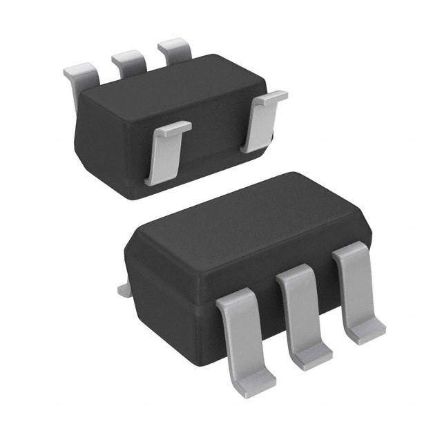
| 产品图片 |
|
| 产品型号 | TLVH431BIDBVR |
| rohs | 无铅 / 符合限制有害物质指令(RoHS)规范要求 |
| 产品系列 | - |
| 供应商器件封装 | SOT-23-5 |
| 其它名称 | 296-17686-6 |
| 包装 | 剪切带 (CT) |
| 参考类型 | 旁路,可调节,精度 |
| 安装类型 | 表面贴装 |
| 容差 | ±0.5% |
| 封装/外壳 | SC-74A,SOT-753 |
| 工作温度 | -40°C ~ 85°C |
| 标准包装 | 1 |
| 温度系数 | 138ppm/°C |
| 电压-输入 | - |
| 电压-输出 | 1.24 V ~ 18 V |
| 电流-输出 | 70mA |
| 电流-阴极 | 100µA |
| 电流-静态 | - |
| 通道数 | 1 |


PDF Datasheet 数据手册内容提取
Product Sample & Technical Tools & Support & Folder Buy Documents Software Community TLVH431,TLVH431A,TLVH431B TLVH432,TLVH432A,TLVH432B SLVS555K–NOVEMBER2004–REVISEDSEPTEMBER2016 TLVH431, TLVH432 Low-Voltage Adjustable Precision Shunt Regulators 1 Features 3 Description • Low-VoltageOperation:Downto1.24V The TLVH431 and TLVH432 devices are low-voltage 1 3-terminal adjustable voltage references, with • ReferenceVoltageTolerancesat25°C specified thermal stability over applicable industrial – 0.5%forBGrade and commercial temperature ranges. Output voltage – 1%forAGrade can be set to any value between VREF (1.24 V) and 18 V with two external resistors (see Figure 19). – 1.5%forStandardGrade These devices operate from a lower voltage (1.24 V) • AdjustableOutputVoltage,VO=VREF to18V than the widely used TL431 and TL1431 shunt- • WideOperatingCathodeCurrentRange: regulatorreferences. 100μAto70mA When used with an optocoupler, the TLVH431 and • 0.25-Ω TypicalOutputImpedance TLVH432 devices are ideal voltage references in • –40°Cto+125°CSpecifications isolated feedback circuits for 3-V to 3.3-V switching- mode power supplies. They have a typical output • TLVH432ProvidesAlternativePinoutsfor impedance of 0.25 Ω. Active output circuitry provides SOT-23-3andSOT-89Packages a very sharp turn-on characteristic, making the • Ultra-SmallSC-70PackageOffers40% TLVH431 and TLVH432 devices excellent SmallerFootprintthanSOT-23-3 replacements for low-voltage Zener diodes in many applications, including on-board regulation and 2 Applications adjustablepowersupplies. • AdjustableVoltageandCurrentReferencing The TLVH432 device is identical to the TLVH431 device, but is offered with different pinouts for the • SecondarySideRegulationinFlybackSMPSs 3-pinSOT-23andSOT-89packages. • ZenerReplacement • VoltageMonitoring DeviceInformation(1) • ComparatorwithIntegratedReference PARTNUMBER PACKAGE BODYSIZE(NOM) TLVH43xxDBZ SOT-23(5) 2.90mm×1.60mm TLVH43xxDBZ SOT-23(3) 2.92mm×1.30mm TLVH43xxDCK SC70(6) 2.00mm×1.25mm TLVH43xxLP TO-92(3) 4.30mm×4.30mm TLVH43xxPK SOT-89(3) 4.50mm×2.50mm (1) For all available packages, see the orderable addendum at theendofthedatasheet. SimplifiedSchematic Input VO IK VREF 1 An IMPORTANT NOTICE at the end of this data sheet addresses availability, warranty, changes, use in safety-critical applications, intellectualpropertymattersandotherimportantdisclaimers.PRODUCTIONDATA.
TLVH431,TLVH431A,TLVH431B TLVH432,TLVH432A,TLVH432B SLVS555K–NOVEMBER2004–REVISEDSEPTEMBER2016 www.ti.com Table of Contents 1 Features.................................................................. 1 8.3 FeatureDescription.................................................17 2 Applications........................................................... 1 8.4 DeviceFunctionalModes........................................18 3 Description............................................................. 1 9 ApplicationsandImplementation...................... 19 4 RevisionHistory..................................................... 2 9.1 ApplicationInformation............................................19 9.2 TypicalApplications................................................20 5 PinConfigurationandFunctions......................... 3 10 PowerSupplyRecommendations..................... 24 6 Specifications......................................................... 4 11 Layout................................................................... 24 6.1 AbsoluteMaximumRatings......................................4 6.2 ESDRatings..............................................................4 11.1 LayoutGuidelines.................................................24 6.3 RecommendedOperatingConditions.......................4 11.2 LayoutExample....................................................24 6.4 ThermalInformation..................................................4 12 DeviceandDocumentationSupport................. 25 6.5 TLVH43xElectricalCharacteristics...........................5 12.1 DocumentationSupport........................................25 6.6 TLVH43xAElectricalCharacteristics........................6 12.2 ReceivingNotificationofDocumentationUpdates25 6.7 TLVH43xBElectricalCharacteristics........................7 12.3 CommunityResources..........................................25 6.8 TypicalCharacteristics..............................................8 12.4 RelatedLinks........................................................25 7 ParameterMeasurementInformation................15 12.5 Trademarks...........................................................25 12.6 ElectrostaticDischargeCaution............................25 8 DetailedDescription............................................ 16 12.7 Glossary................................................................25 8.1 Overview.................................................................16 13 Mechanical,Packaging,andOrderable 8.2 FunctionalBlockDiagram.......................................16 Information........................................................... 26 4 Revision History NOTE:Pagenumbersforpreviousrevisionsmaydifferfrompagenumbersinthecurrentversion. ChangesfromRevisionJ(January2015)toRevisionK Page • Changeddatasheettitle......................................................................................................................................................... 1 • UpdatedpinoutimagesandPinFunctionstable.................................................................................................................... 3 • DeletedDpackagefromPinFunctionstable......................................................................................................................... 3 • AddedReceivingNotificationofDocumentationUpdatessectionandCommunityResourcessection.............................. 25 ChangesfromRevisionI(September2009)toRevisionJ Page • AddedApplications,DeviceInformationtable,PinFunctionstable,ESDRatingstable,ThermalInformationtable, TypicalCharacteristics,FeatureDescriptionsection,DeviceFunctionalModes,ApplicationandImplementation section,PowerSupplyRecommendationssection,Layoutsection,DeviceandDocumentationSupportsection,and Mechanical,Packaging,andOrderableInformationsection.................................................................................................. 1 • DeletedOrderingInformationtable........................................................................................................................................ 1 2 SubmitDocumentationFeedback Copyright©2004–2016,TexasInstrumentsIncorporated ProductFolderLinks:TLVH431 TLVH431A TLVH431BTLVH432 TLVH432A TLVH432B
TLVH431,TLVH431A,TLVH431B TLVH432,TLVH432A,TLVH432B www.ti.com SLVS555K–NOVEMBER2004–REVISEDSEPTEMBER2016 5 Pin Configuration and Functions TLVH431DBVPackage 5-PinSOT-23 TLVH431DBZPackage TopView 3-PinSOT-23 TopView NC 1 5 ANODE REF 1 * 2 3 ANODE CATHODE 3 4 REF CATHODE 2 Not to scale Not to scale NC–Nointernalconnection TLVH432DBZPackage *Pin2isattachedtoSubstrateandmust 3-PinSOT-23 beconnectedtoANODEorleftopen. TopView TLVH431DCKPackage 6-PinSC70 CATHODE 1 TopView 3 ANODE REF 2 CATHODE 1 6 ANODE Not to scale NC 2 5 NC REF 3 4 NC TLVH431PKPackage 3-PinSOT-89 Not to scale TopView TLVH431LPPackage 3 CATHODE 3-PinTO-92 TopView 2 ANODE 1 REF 1 CATHODE Not to scale 2 ANODE 3 REF TLVH432PKPackage 3-PinSOT-89 Not to scale TopView 3 REF 2 ANODE 1 CATHODE Not to scale PinFunctions PIN TLVH431 TLVH432 TYPE DESCRIPTION NAME DBZ DBV LP DCK PK DBZ PK CATHODE 2 3 1 1 3 1 1 I/O ShuntCurrent/Voltageinput REF 1 4 3 3 1 2 3 I Thresholdrelativetocommonanode ANODE 3 5 2 6 2 3 2 O Commonpin,normallyconnectedtoground NC — 1 — 2,4,5 — — — I NoInternalConnection * — 2 — — — — — I SubstrateConnection Copyright©2004–2016,TexasInstrumentsIncorporated SubmitDocumentationFeedback 3 ProductFolderLinks:TLVH431 TLVH431A TLVH431BTLVH432 TLVH432A TLVH432B
TLVH431,TLVH431A,TLVH431B TLVH432,TLVH432A,TLVH432B SLVS555K–NOVEMBER2004–REVISEDSEPTEMBER2016 www.ti.com 6 Specifications 6.1 Absolute Maximum Ratings overoperatingfree-airtemperaturerange(unlessotherwisenoted)(1) MIN MAX UNIT V Cathodevoltage(2) 20 V KA I Cathodecurrent –25 80 mA K I Referencecurrent –0.05 3 mA ref T Operatingvirtualjunctiontemperature 150 °C J T Storagetemperature –65 150 °C stg (1) StressesbeyondthoselistedunderAbsoluteMaximumRatingsmaycausepermanentdamagetothedevice.Thesearestressratings only,whichdonotimplyfunctionaloperationofthedeviceattheseoranyotherconditionsbeyondthoseindicatedunderRecommended OperatingConditions.Exposuretoabsolute-maximum-ratedconditionsforextendedperiodsmayaffectdevicereliability. (2) Voltagevaluesarewithrespecttotheanodeterminal,unlessotherwisenoted. 6.2 ESD Ratings VALUE UNIT Electrostatic Humanbodymodel(HBM),perANSI/ESDA/JEDECJS-001(1) ±2000 V V (ESD) discharge Chargeddevicemodel(CDM),perJEDECspecificationJESD22-C101(2) ±1000 (1) JEDECdocumentJEP155statesthat500-VHBMallowssafemanufacturingwithastandardESDcontrolprocess. (2) JEDECdocumentJEP157statesthat250-VCDMallowssafemanufacturingwithastandardESDcontrolprocess. 6.3 Recommended Operating Conditions See(1) MIN MAX UNIT V Cathodevoltage V 18 V KA REF I Cathodecurrent(continuous) 0.1 70 mA K TLVH43x_C 0 70 T Operatingfree-airtemperature TLVH43x_I –40 85 °C A TLVH43x_Q –40 125 (1) MaximumpowerdissipationisafunctionofT(max),θ ,andT .Themaximumallowablepowerdissipationatanyallowableambient J JA A temperatureisP =(T(max)–T )/θ .OperatingattheabsolutemaximumT of150°Ccanaffectreliability. D J A JA J 6.4 Thermal Information TLVH43xx THERMALMETRIC(1) DCK PK DBV DBZ LP UNIT (SC70) (SOT-89) (SOT-23) (SOT-23) (TO-92) 6PINS 3PINS 5PINS 3PINS 3PINS R Junction-to-ambientthermalresistance 87 52 206 206 140 °C/W θJA R Junction-to-case(top)thermalresistance 259 9 131 76 55 °C/W θJC(top) (1) Formoreinformationabouttraditionalandnewthermalmetrics,seetheSemiconductorandICPackageThermalMetricsapplication report. 4 SubmitDocumentationFeedback Copyright©2004–2016,TexasInstrumentsIncorporated ProductFolderLinks:TLVH431 TLVH431A TLVH431BTLVH432 TLVH432A TLVH432B
TLVH431,TLVH431A,TLVH431B TLVH432,TLVH432A,TLVH432B www.ti.com SLVS555K–NOVEMBER2004–REVISEDSEPTEMBER2016 6.5 TLVH43x Electrical Characteristics at25°Cfree-airtemperature(unlessotherwisenoted) TLVH431 PARAMETER TESTCONDITIONS TLVH432 UNIT MIN TYP MAX T =25°C 1.222 1.24 1.258 A V =V , TLVH431C 1.21 1.27 VREF Referencevoltage IKK=A10mREAF TSAee=Ffuigllurraen1g8e(,1) TLVH431I 1.202 1.278 V TLVH431Q 1.194 1.286 TLVH431C 4 12 VREF(dev) VteRmEpFedreavtuiaretiornanogvee(r2)full VKA=VREF,IK=10mA,SeeFigure18(1) TLVH431I 6 20 mV TLVH431Q 11 31 (cid:1)V (cid:1)VREF RcaatthioodoefVvoRlEtaFgcehacnhgaengtoe IK=10mA,VK=VREFto18V,SeeFigure19 –1.5 –2.7 mV/V KA I Referenceterminalcurrent I =10mA,R1=10kΩ,R2=open,SeeFigure19 0.1 0.5 μA ref K TLVH431C 0.05 0.3 I deviationoverfull I =10mA,R1=10kΩ,R2=open, Iref(dev) treemf peraturerange(2) SKeeFigure19(1) TLVH431I 0.1 0.4 μA TLVH431Q 0.15 0.5 Minimumcathodecurrent I V =V ,SeeFigure18 60 100 μA K(min) forregulation KA REF I Off-statecathodecurrent V =0,V =18V,SeeFigure20 0.02 0.1 μA K(off) REF KA |z | Dynamicimpedance(3) VKA=VREF,f≤1kHz,IK=0.1mAto70mA, 0.25 0.4 Ω KA SeeFigure18 (1) Fulltemperaturerangesare–40°Cto+125°CforTLVH431Q,–40°Cto+85°CforTLVH431I,and0°Cto70°CforTLVH431C. (2) ThedeviationparametersV andI aredefinedasthedifferencesbetweenthemaximumandminimumvaluesobtainedover REF(dev) ref(dev) theratedtemperaturerange.Theaveragefull-rangetemperaturecoefficientofthereferenceinputvoltage,αV ,isdefinedas: REF æ V ö ç REF(dev) ÷´106 æppmö èV (T =25°C)ø aV ç ÷= REF A REF è °C ø DT A whereΔT istheratedoperatingfree-airtemperaturerangeofthedevice. A αV canbepositiveornegative,dependingonwhetherminimumV ormaximumV ,respectively,occursatthelower REF REF REF temperature. (3) Thedynamicimpedanceisdefinedas: DV z = KA ka DI K Whenthedeviceisoperatingwithtwoexternalresistors(seeFigure19),thetotaldynamicimpedanceofthecircuitisdefinedas: DV æ R1ö z ¢= » z ´ç1+ ÷ ka DI ka è R2ø Copyright©2004–2016,TexasInstrumentsIncorporated SubmitDocumentationFeedback 5 ProductFolderLinks:TLVH431 TLVH431A TLVH431BTLVH432 TLVH432A TLVH432B
TLVH431,TLVH431A,TLVH431B TLVH432,TLVH432A,TLVH432B SLVS555K–NOVEMBER2004–REVISEDSEPTEMBER2016 www.ti.com 6.6 TLVH43xA Electrical Characteristics at25°Cfree-airtemperature(unlessotherwisenoted) TLVH431A PARAMETER TESTCONDITIONS TLVH432A UNIT MIN TYP MAX T =25°C 1.228 1.24 1.252 A V =V , TLVH431AC 1.221 1.259 VREF Referencevoltage IKK=A10mREAF TSAee=Ffuigllurraen1g8e(,1) TLVH431AI 1.215 1.265 V TLVH431AQ 1.209 1.271 TLVH431AC 4 12 VREF(dev) VteRmEpFedreavtuiaretiornanogvee(r2)full VKA=VREF,IK=10mA,SeeFigure18(1) TLVH431AI 6 20 mV TLVH431AQ 11 31 (cid:1)V (cid:1)VREF RcaatthioodoefVvoRlEtaFgcehacnhgaengtoe VK=VREFto18V,IK=10mA,SeeFigure19 –1.5 –2.7 mV/V KA I Referenceterminalcurrent I =10mA,R1=10kΩ,R2=open,SeeFigure19 0.1 0.5 μA ref K TLVH431AC 0.05 0.3 I deviationoverfull I =10mA,R1=10kΩ,R2=open, Iref(dev) treemf peraturerange(2) SKeeFigure19(1) TLVH431AI 0.1 0.4 μA TLVH431AQ 0.15 0.5 Minimumcathodecurrent I V =V ,SeeFigure18 60 100 μA K(min) forregulation KA REF I Off-statecathodecurrent V =0,V =18V,SeeFigure20 0.02 0.1 μA K(off) REF KA |z | Dynamicimpedance(3) VKA=VREF,f≤1kHz,IK=0.1mAto70mA, 0.25 0.4 Ω KA SeeFigure18 (1) Fulltemperaturerangesare–40°Cto+125°CforTLVH431Q,–40°Cto+85°CforTLVH431I,and0°Cto70°CforTLVH431C. (2) ThedeviationparametersV andI aredefinedasthedifferencesbetweenthemaximumandminimumvaluesobtainedover REF(dev) ref(dev) theratedtemperaturerange.Theaveragefull-rangetemperaturecoefficientofthereferenceinputvoltage,αV ,isdefinedas: REF æ V ö ç REF(dev) ÷´106 æppmö èV (T =25°C)ø aV ç ÷= REF A REF è °C ø DT A whereΔT istheratedoperatingfree-airtemperaturerangeofthedevice. A αV canbepositiveornegative,dependingonwhetherminimumV ormaximumV ,respectively,occursatthelower REF REF REF temperature. (3) Thedynamicimpedanceisdefinedas: DV z = KA ka DI K Whenthedeviceisoperatingwithtwoexternalresistors(seeFigure19),thetotaldynamicimpedanceofthecircuitisdefinedas: DV æ R1ö z ¢= » z ´ç1+ ÷ ka DI ka è R2ø 6 SubmitDocumentationFeedback Copyright©2004–2016,TexasInstrumentsIncorporated ProductFolderLinks:TLVH431 TLVH431A TLVH431BTLVH432 TLVH432A TLVH432B
TLVH431,TLVH431A,TLVH431B TLVH432,TLVH432A,TLVH432B www.ti.com SLVS555K–NOVEMBER2004–REVISEDSEPTEMBER2016 6.7 TLVH43xB Electrical Characteristics at25°Cfree-airtemperature(unlessotherwisenoted) TLVH431B PARAMETER TESTCONDITIONS TLVH432B UNIT MIN TYP MAX T =25°C 1.234 1.24 1.246 A V =V , TLVH431BC 1.227 1.253 VREF Referencevoltage IKK=A10mREAF TSAee=Ffuigllurraen1g8e(,1) TLVH431BI 1.224 1.259 V TLVH431BQ 1.221 1.265 TLVH431BC 4 12 VREF(dev) VteRmEpFedreavtuiaretiornanogvee(r2)full VKA=VREF,IK=10mA,SeeFigure18(1) TLVH431BI 6 20 mV TLVH431BQ 11 31 (cid:1)V (cid:1)VREF RcaatthioodoefVvoRlEtaFgcehacnhgaengtoe IK=10mA,VK=VREFto18V,SeeFigure19 –1.5 –2.7 mV/V KA I Referenceterminalcurrent I =10mA,R1=10kΩ,R2=open,SeeFigure19 0.1 0.5 μA ref K TLVH431BC 0.05 0.3 I deviationoverfull I =10mA,R1=10kΩ,R2=open, Iref(dev) treemf peraturerange(2) SKeeFigure19(1) TLVH431BI 0.1 0.4 μA TLVH431BQ 0.15 0.5 Minimumcathodecurrent I V =V ,SeeFigure18 60 100 μA K(min) forregulation KA REF I Off-statecathodecurrent V =0,V =18V,SeeFigure20 0.02 0.1 μA K(off) REF KA |z | Dynamicimpedance(3) V =V ,f≤1kHz,I =0.1mAto70mA,SeeFigure18 0.25 0.4 Ω KA KA REF K (1) Fulltemperaturerangesare–40°Cto+125°CforTLVH431Q,–40°Cto+85°CforTLVH431I,and0°Cto70°CforTLVH431C. (2) ThedeviationparametersV andI aredefinedasthedifferencesbetweenthemaximumandminimumvaluesobtainedover REF(dev) ref(dev) theratedtemperaturerange.Theaveragefull-rangetemperaturecoefficientofthereferenceinputvoltage,αV ,isdefinedas: REF æ V ö ç REF(dev) ÷´106 æppmö èV (T =25°C)ø aV ç ÷= REF A REF è °C ø DT A whereΔT istheratedoperatingfree-airtemperaturerangeofthedevice. A αV canbepositiveornegative,dependingonwhetherminimumV ormaximumV ,respectively,occursatthelower REF REF REF temperature. (3) Thedynamicimpedanceisdefinedas: DV z = KA ka DI K Whenthedeviceisoperatingwithtwoexternalresistors(seeFigure19),thetotaldynamicimpedanceofthecircuitisdefinedas: DV æ R1ö z ¢= » z ´ç1+ ÷ ka DI ka è R2ø Copyright©2004–2016,TexasInstrumentsIncorporated SubmitDocumentationFeedback 7 ProductFolderLinks:TLVH431 TLVH431A TLVH431BTLVH432 TLVH432A TLVH432B
TLVH431,TLVH431A,TLVH431B TLVH432,TLVH432A,TLVH432B SLVS555K–NOVEMBER2004–REVISEDSEPTEMBER2016 www.ti.com 6.8 Typical Characteristics OperationofthedeviceattheseoranyotherconditionsbeyondthoseindicatedintheRecommendedOperatingConditions tablearenotimplied. 1.254 250 IK= 10 mA 230 IK=10mA 1.252 R1 = 10 kΩ nA 210 R2 = Open V 1.250 − −oReferencltage−e V 111...222444684 eferenceInputCurrent 111111357900000 Vref 1.242 −R 90 ef 1.240 Ir 70 1.238 50 −50 −25 0 25 50 75 100 125 150 −50 −25 0 25 50 75 100 125 150 TJ−Junction Temperature−°C TJ−Junction Temperature−°C Figure1.ReferenceVoltage vsJunctionTemperature Figure2.ReferenceInputCurrent vsJunctionTemperature 70 250 ~~ VKA= VREF VKA=VREF TA= 25°C 200 TA= 25°C 10 mA ~~ A 150 − 5 µ− 100 Cathode Current −05 Cathode Current −55000 −IK −IK −−110500 −10 −200 −15 −250 −1 −0.5 0 0.5 1 1.5 −1 −0.5 0 0.5 1 1.5 VKA−Cathode Voltage−V VKA−CathodeVoltage−V Figure3.CathodeCurrent Figure4.CathodeCurrent vsCathodeVoltage vsCathodeVoltage 120 4000 111105 nA 3500 VVKRAEF== 50 V − 105 ent 3000 100 urr C 95 e 2500 Ik(min) 889050 ate Cathod 2000 75 Off-St 1500 70 − 1000 65 off) 60 K( 500 I 55 -40 -20 0 20 40 60 80 100 120 140 0 Temperature (qC) −50 −25 0 25 50 75 100 125 150 Figure5.MinimumCathodeCurrentvs.Temperature TJ−Junction Temperature−°C Figure6.Off-StateCathodeCurrent vsJunctionTemperature 8 SubmitDocumentationFeedback Copyright©2004–2016,TexasInstrumentsIncorporated ProductFolderLinks:TLVH431 TLVH431A TLVH431BTLVH432 TLVH432A TLVH432B
TLVH431,TLVH431A,TLVH431B TLVH432,TLVH432A,TLVH432B www.ti.com SLVS555K–NOVEMBER2004–REVISEDSEPTEMBER2016 Typical Characteristics (continued) OperationofthedeviceattheseoranyotherconditionsbeyondthoseindicatedintheRecommendedOperatingConditions tablearenotimplied. 0.00 0.025 age −0.1 IK= 10 mA IK= 1 mA atiolto of Delta Reference V oltage−Cathode VmV/V −−−−−00000.....65432 ΔVKA= VREFto 18 V Vref−%age Change in Vref −−0.00.20550 % Change (3δ%) Change (avg) Δ−RVKAto Delta −−00..87 Percent −0−.007.51 ef/ −0.9 Vr % Change (−3δ) Δ −1−.10 −0.125 −50 −25 0 25 50 75 100 125 150 0 10 20 30 40 50 60 TJ−Junction Temperature−°C Operating Life at 55°C−kh(1) (1)Extrapolatedfromlife-testdatatakenat125°C;theactivationenergy assumedis 0.7 eV. Figure7.RatioofDeltaReferenceVoltagetoDeltaCathode Figure8.PercentageChangeinV REF Voltage vs vsJunctionTemperature OperatingLifeat55°C EQUIVALENT INPUT NOISE VOLTAGE vs FREQUENCY 350 3 V Hz) VKA= VREF V/ IK= 1 mA 1 kW (n TA= 25°C − 300 e g + 750W olta 470mF 2200mF TLE2027 e V + + s oi 250 _ TP N ut TLVH431 820W p n TLVH432 nt I 160 kW e al 200 160W v ui q E − n V TEST CIRCUIT FOR EQUIVALENT INPUT NOISE VOLTAGE 150 10 100 1 k 10 k 100 k f–Frequency–(Hz) Figure9.EquivalentInputNoiseVoltage Copyright©2004–2016,TexasInstrumentsIncorporated SubmitDocumentationFeedback 9 ProductFolderLinks:TLVH431 TLVH431A TLVH431BTLVH432 TLVH432A TLVH432B
TLVH431,TLVH431A,TLVH431B TLVH432,TLVH432A,TLVH432B SLVS555K–NOVEMBER2004–REVISEDSEPTEMBER2016 www.ti.com Typical Characteristics (continued) OperationofthedeviceattheseoranyotherconditionsbeyondthoseindicatedintheRecommendedOperatingConditions tablearenotimplied. EQUIVALENT INPUT NOISE VOLTAGE OVERA10-S PERIOD 10 f= 0.1 Hz to 10 Hz V) 8 m IK= 1 mA ( e− 6 TA= 25°C g a olt 4 V e ois 2 N ut 0 p n nt I −2 e al v −4 ui q E −6 − n V −8 −10 0 2 4 6 8 10 t−Time−(s) 3 V 1 kW + 0.47mF 750W 470mF 2200mF TLE2027 + + 10 kW 10 kW TLE2027 2.2mF TP + _ + 820W _ 160 kW 1mF TLVH431 CRO 1 MW TLVH432 33 kW 0.1mF 33 kW 16W TEST CIRCUIT FOR 0.1-Hz TO 10-Hz EQUIVALENT NOISE VOLTAGE Figure10.EquivalentInputNoiseVoltage 10 SubmitDocumentationFeedback Copyright©2004–2016,TexasInstrumentsIncorporated ProductFolderLinks:TLVH431 TLVH431A TLVH431BTLVH432 TLVH432A TLVH432B
TLVH431,TLVH431A,TLVH431B TLVH432,TLVH432A,TLVH432B www.ti.com SLVS555K–NOVEMBER2004–REVISEDSEPTEMBER2016 Typical Characteristics (continued) OperationofthedeviceattheseoranyotherconditionsbeyondthoseindicatedintheRecommendedOperatingConditions tablearenotimplied. SMALL-SIGNALVOLTAGE GAIN /PHASE MARGIN vs FREQUENCY B) 80 0° (d IK= 10 mA gin− 70 TA= 25°C 36° hift Output Mar 60 72° e S 6.8 kW IK hase 50 108° Phas 10mF 180W P n/ 40 144° ai G 5 V e 30 180° g 4.3 kW a olt 20 V nal 10 g GND Si all- 0 m −S −10 TEST CIRCUIT FOR VOLTAGE GAIN V AND PHASE MARGIN −20 A 100 1 k 10 k 100 k 1 M f−Frequency−(Hz) Figure11.VoltageGainandPhaseMargin PULSERESPONSE1 3.5 R=18kΩ Input TA= 25°C 3 18 kΩ Output V 2.5 − e ag Ik Volt 2 Pulse ut Generator 50Ω utp 1.5 Output f = 100 kHz O nd 1 a ut GND p n 0.5 I 0 TEST CIRCUIT FOR PULSE RESPONSE 1 −0.5 0 1 2 3 4 5 6 7 8 t−Time−µs Figure12.PulseResponse1 Copyright©2004–2016,TexasInstrumentsIncorporated SubmitDocumentationFeedback 11 ProductFolderLinks:TLVH431 TLVH431A TLVH431BTLVH432 TLVH432A TLVH432B
TLVH431,TLVH431A,TLVH431B TLVH432,TLVH432A,TLVH432B SLVS555K–NOVEMBER2004–REVISEDSEPTEMBER2016 www.ti.com Typical Characteristics (continued) OperationofthedeviceattheseoranyotherconditionsbeyondthoseindicatedintheRecommendedOperatingConditions tablearenotimplied. PULSERESPONSE2 3.5 R = 1.8 kΩ Input TA= 25°C 3 1.8 kΩ Output V 2.5 − e ag IK Volt 2 Pulse ut Generator 50Ω utp 1.5 Output f = 100 kHz O nd 1 a ut GND p n 0.5 I 0 TEST CIRCUIT FOR PULSE RESPONSE 2 −0.5 0 1 2 3 4 5 6 7 8 t−Time−µs Figure13.PulseResponse2 30 kW I K 50W 100 µF I C 2 L I 1 Figure14.PhaseMarginTestCircuit 12 SubmitDocumentationFeedback Copyright©2004–2016,TexasInstrumentsIncorporated ProductFolderLinks:TLVH431 TLVH431A TLVH431BTLVH432 TLVH432A TLVH432B
TLVH431,TLVH431A,TLVH431B TLVH432,TLVH432A,TLVH432B www.ti.com SLVS555K–NOVEMBER2004–REVISEDSEPTEMBER2016 Typical Characteristics (continued) OperationofthedeviceattheseoranyotherconditionsbeyondthoseindicatedintheRecommendedOperatingConditions tablearenotimplied. I K Figure15.PhaseMarginvsCapacitiveLoad V =V (1.25V),T =25°C KA REF A I K Figure16.PhaseMarginvsCapacitiveLoad V =2.50V,T =25°C KA A Copyright©2004–2016,TexasInstrumentsIncorporated SubmitDocumentationFeedback 13 ProductFolderLinks:TLVH431 TLVH431A TLVH431BTLVH432 TLVH432A TLVH432B
TLVH431,TLVH431A,TLVH431B TLVH432,TLVH432A,TLVH432B SLVS555K–NOVEMBER2004–REVISEDSEPTEMBER2016 www.ti.com Typical Characteristics (continued) OperationofthedeviceattheseoranyotherconditionsbeyondthoseindicatedintheRecommendedOperatingConditions tablearenotimplied. I K Figure17.PhaseMarginvsCapacitiveLoad V =5.00V,T =25°C KA A 14 SubmitDocumentationFeedback Copyright©2004–2016,TexasInstrumentsIncorporated ProductFolderLinks:TLVH431 TLVH431A TLVH431BTLVH432 TLVH432A TLVH432B
TLVH431,TLVH431A,TLVH431B TLVH432,TLVH432A,TLVH432B www.ti.com SLVS555K–NOVEMBER2004–REVISEDSEPTEMBER2016 7 Parameter Measurement Information Input V O I K V REF Figure18. TestCircuitforV =V ,V =V =V KA REF O KA REF Input V O I K R1 I ref R2 V REF Figure19. TestCircuitforV >V ,V =V =V ×(1+R1/R2)+I × R1 KA REF O KA REF ref Input V O I K(off) Figure20. TestCircuitforI K(off) Copyright©2004–2016,TexasInstrumentsIncorporated SubmitDocumentationFeedback 15 ProductFolderLinks:TLVH431 TLVH431A TLVH431BTLVH432 TLVH432A TLVH432B
TLVH431,TLVH431A,TLVH431B TLVH432,TLVH432A,TLVH432B SLVS555K–NOVEMBER2004–REVISEDSEPTEMBER2016 www.ti.com 8 Detailed Description 8.1 Overview TLVH431 is a low power counterpart to TL431, having lower reference voltage (1.24 V versus 2.5 V) for lower voltage adjustability and lower minimum cathode current (I = 100 µA versus 1 mA). Like TL431, TLVH431 is k(min) used in conjunction with its key components to behave as a single voltage reference, error amplifier, voltage clamporcomparatorwithintegratedreference. TLVH431 is also a higher voltage counterpart to TLV431, with cathode voltage adjustability from 1.24 V to 18 V, makingthispartoptimumforawiderangeofendequipmentsinindustrial,auto,telecomandcomputing.Inorder for this device to behave as a shunt regulator or error amplifier, >100 µA (I (max)) must be supplied in to the min cathode pin. Under this condition, feedback can be applied from the Cathode and Ref pins to create a replica of theinternalreferencevoltage. Various reference voltage options can be purchased with initial tolerances (at 25°C) of 0.5%, 1%, and 1.5%. ThesereferenceoptionsaredenotedbyB(0.5%),A(1.0%)andblank(1.5%)aftertheTLVH431. The TLVH431xC devices are characterized for operation from 0°C to 70°C, the TLVH431xI devices are characterized for operation from –40°C to +85°C, and the TLVH431xQ devices are characterized for operation from –40°Cto+125°C. 8.2 Functional Block Diagram CATHODE REF + − V = 1.24 V REF ANODE Figure21. EquivalentSchematic 16 SubmitDocumentationFeedback Copyright©2004–2016,TexasInstrumentsIncorporated ProductFolderLinks:TLVH431 TLVH431A TLVH431BTLVH432 TLVH432A TLVH432B
TLVH431,TLVH431A,TLVH431B TLVH432,TLVH432A,TLVH432B www.ti.com SLVS555K–NOVEMBER2004–REVISEDSEPTEMBER2016 Functional Block Diagram (continued) Cathode REF Anode Figure22. DetailedSchematic 8.3 Feature Description TLVH431 consists of an internal reference and amplifier that outputs a sink current base on the difference betweenthereferencepinandthevirtualinternalpin.ThesinkcurrentisproducedbyaninternalDarlingtonpair. When operated with enough voltage headroom (≥ 1.24 V) and cathode current (I ), TLVH431 forces the ka reference pin to 1.24 V. However, the reference pin can not be left floating, as it needs Iref ≥ 0.5 µA (see Specifications). This is because the reference pin is driven into an NPN, which needs base current in order operateproperly. WhenfeedbackisappliedfromtheCathodeandReferencepins,TLVH431behavesasaZenerdiode,regulating to a constant voltage dependent on current being supplied into the cathode. This is due to the internal amplifier and reference entering the proper operating regions. The same amount of current needed in the above feedback situation must be applied to this device in open loop, servo or error amplifying implementations in order for it to beintheproperlinearregiongivingTLVH431enoughgain. Unlike many linear regulators, TLVH431 is internally compensated to be stable without an output capacitor between the cathode and anode. However, if it is desired to use an output capacitor Figure 15, Figure 16, and Figure17canbeusedasaguidetoassistinchoosingthecorrectcapacitortomaintainstability. Copyright©2004–2016,TexasInstrumentsIncorporated SubmitDocumentationFeedback 17 ProductFolderLinks:TLVH431 TLVH431A TLVH431BTLVH432 TLVH432A TLVH432B
TLVH431,TLVH431A,TLVH431B TLVH432,TLVH432A,TLVH432B SLVS555K–NOVEMBER2004–REVISEDSEPTEMBER2016 www.ti.com 8.4 Device Functional Modes 8.4.1 OpenLoop(Comparator) When the cathode/output voltage or current of TLVH431 is not being fed back to the reference/input pin in any form, this device is operating in open loop. With proper cathode current (I ) applied to this device, TLVH431 has ka the characteristics shown in Figure 4. With such high gain in this configuration, the TLVH431 device is typically used as a comparator. With the reference integrated makes TLVH431 the preferred choice when users are trying tomonitoracertainlevelofasinglesignal. 8.4.2 ClosedLoop When the cathode/output voltage or current of TLVH431 is being fed back to the reference/input pin in any form, this device is operating in closed loop. The majority of applications involving TLVH431 use it in this manner to regulate a fixed voltage or current. The feedback enables this device to behave as an error amplifier, computing a portion of the output voltage and adjusting it to maintain the desired regulation. This is done by relating the outputvoltagebacktothereferencepininamannertomakeitequaltotheinternalreferencevoltage,whichcan beaccomplishedthroughresistiveordirectfeedback. 18 SubmitDocumentationFeedback Copyright©2004–2016,TexasInstrumentsIncorporated ProductFolderLinks:TLVH431 TLVH431A TLVH431BTLVH432 TLVH432A TLVH432B
TLVH431,TLVH431A,TLVH431B TLVH432,TLVH432A,TLVH432B www.ti.com SLVS555K–NOVEMBER2004–REVISEDSEPTEMBER2016 9 Applications and Implementation NOTE Information in the following applications sections is not part of the TI component specification, and TI does not warrant its accuracy or completeness. TI’s customers are responsible for determining suitability of components for their purposes. Customers should validateandtesttheirdesignimplementationtoconfirmsystemfunctionality. 9.1 Application Information Figure23showstheTLVH431,TLVH431A,orTLVH431Busedina3.3-Visolatedflybacksupply.Outputvoltage V can be as low as reference voltage V (1.24 V ± 1%). The output of the regulator, plus the forward voltage O REF drop of the optocoupler LED (1.24 + 1.4 = 2.64 V), determine the minimum voltage that can be regulated in an isolated supply configuration. Regulated voltage as low as 2.7 Vdc is possible in the topology shown in Figure23. The TLVH431 family of devices are prevalent in these applications, being designers go to choice for secondary sideregulation.Duetothisprevalence,thissectionexplainsoperationanddesigninbothstatesofTLVH431that thisapplicationwillsee,openloop(Comparator+V )andclosedloop(ShuntRegulator). REF Further information about system stability and using a TLVH431 device for compensation see Compensation DesignWithTL431forUCC28600,SLUA671. ~ V I 120 V − + P ~ V O 3.3 V P P Gate Drive V CC Controller V FB TLVH431 Current Sense GND P P P P Figure23. FlybackWithIsolationUsingTLVH431orTLVH432 asVoltageReferenceandErrorAmplifier Copyright©2004–2016,TexasInstrumentsIncorporated SubmitDocumentationFeedback 19 ProductFolderLinks:TLVH431 TLVH431A TLVH431BTLVH432 TLVH432A TLVH432B
TLVH431,TLVH431A,TLVH431B TLVH432,TLVH432A,TLVH432B SLVS555K–NOVEMBER2004–REVISEDSEPTEMBER2016 www.ti.com 9.2 Typical Applications 9.2.1 ComparatorWithIntegratedReference(OpenLoop) Vsup Rsup Vout CATHODE R1 V L R V IN REF IN + R2 1.24 V ANODE Figure24. ComparatorApplicationSchematic 9.2.1.1 DesignRequirements Forthisdesignexample,usetheparameterslistedinTable1astheinputparameters. Table1.DesignParameters DESIGNPARAMETER EXAMPLEVALUE InputVoltageRange 0Vto5V InputResistance 10kΩ SupplyVoltage 9V CathodeCurrent(I ) 500µA k OutputVoltageLevel ~1V-V sup LogicInputThresholdsV /V V IH IL L 9.2.1.2 DetailedDesignProcedure WhenusingTLVH431asacomparatorwithreference,determinethefollowing: • Inputvoltagerange • Referencevoltageaccuracy • Outputlogicinputhighandlowlevelthresholds • Currentsourceresistance 9.2.1.2.1 BasicOperation In the configuration shown in Figure 24, TLVH431 behaves as a comparator, comparing the V pin voltage to ref the internal virtual reference voltage. When provided a proper cathode current (I ), TLVH431 will have enough k open loop gain to provide a quick response. With the TLVH431's max Operating Current (I ) being 100 uA and min upto150uAovertemperature,operationbelowthatcouldresultinlowgain,leadingtoaslowresponse. 20 SubmitDocumentationFeedback Copyright©2004–2016,TexasInstrumentsIncorporated ProductFolderLinks:TLVH431 TLVH431A TLVH431BTLVH432 TLVH432A TLVH432B
TLVH431,TLVH431A,TLVH431B TLVH432,TLVH432A,TLVH432B www.ti.com SLVS555K–NOVEMBER2004–REVISEDSEPTEMBER2016 9.2.1.2.2 Overdrive Slow or inaccurate responses can also occur when the reference pin is not provided enough overdrive voltage. This is the amount of voltage that is higher than the internal virtual reference. The internal virtual reference voltagewillbewithintherangeof1.24V ±(0.5%,1.0%or1.5%)dependingonwhichversionisbeingused. The more overdrive voltage provided, the faster the TLVH431 will respond. See figures Figure 25 and Figure 26, fortheoutputresponsestovariousinputvoltages. For applications where TLVH431 is being used as a comparator, it is best to set the trip point to greater than the positive expected error (that is, +1.0% for the A version). For fast response, setting the trip point to > 10% of the internalV shouldsuffice. ref For minimal voltage drop or difference from Vin to the ref pin, it is recommended to use an input resistor <10 kΩ toprovideI . ref 9.2.1.2.3 OutputVoltageandLogicInputLevel In order for TLVH431 to properly be used as a comparator, the logic output must be readable by the receiving logic device. This is accomplished by knowing the input high and low level threshold voltage levels, typically denotedbyV andV . IH IL As shown in Figure 25 and Figure 26, TLVH431's output low level voltage in open-loop/comparator mode is approximately1V,whichissufficientforsome3.3Vsuppliedlogic.However,wouldnotworkfor2.5Vand1.8V supplied logic. To accommodate this a resistive divider can be tied to the output to attenuate the output voltage toavoltagelegibletothereceivinglowvoltagelogicdevice. TLVH431's output high voltage is approximately V due to TLVH431 being open-collector. If V is much SUP SUP higher than the receiving logic's maximum input voltage tolerance, the output must be attenuated to accommodatetheoutgoinglogic'sreliability. When using a resistive divider on the output, be sure to make the sum of the resistive divider (R1 and R2 in Figure 24) is much greater than R in order to not interfere with TLVH431's ability to pull close to V when SUP SUP turningoff. 9.2.1.2.3.1 InputResistance TLVH431 requires an input resistance in this application in order to source the reference current (I ) needed REF from this device to be in the proper operating regions while turning on. The actual voltage seen at the ref pin will be V = V – I × R . Because I can be as high as 0.5 µA, TI recommends to use a resistance small REF IN REF IN REF enoughthatwillmitigatetheerrorthatI createsfromV . REF IN 9.2.1.3 ApplicationCurves 14 10 13 Vin~1.24V (+/-5%) 9 12 VVoo((VViinn==11..1284VV)) 8 Vo(Vin=5.0V) 11 Vin=5.0V Vo(Vin=1.30V) 7 10 6 9 ge (V) 78 ge (V) 45 a a olt 6 olt 3 V V 5 2 4 1 3 0 2 1 -1 0 -2 -0.4 -0.2 0 0.2 0.4 0.6 0.8 -0.4 -0.2 0 0.2 0.4 0.6 0.8 Time (ms) Time (ms) D001 D001 Figure25.OutputResponseWithSmallOverdrive Figure26.OutputResponseWithLargeOverdriveVoltage Voltages Copyright©2004–2016,TexasInstrumentsIncorporated SubmitDocumentationFeedback 21 ProductFolderLinks:TLVH431 TLVH431A TLVH431BTLVH432 TLVH432A TLVH432B
TLVH431,TLVH431A,TLVH431B TLVH432,TLVH432A,TLVH432B SLVS555K–NOVEMBER2004–REVISEDSEPTEMBER2016 www.ti.com 9.2.2 ShuntRegulator/Reference RSUP R1 VSUP V O (1(cid:14) )VREF R2 0R.11% CATH ODE REF VREF TLVH431 CL ANODE R2 0.1% Copyright © 2016, Texas Instruments Incorporated Figure27. ShuntRegulatorSchematic 9.2.2.1 DesignRequirements Forthisdesignexample,usetheparameterslistedinTable2astheinputparameters. Table2.DesignParameters DESIGNPARAMETER EXAMPLEVALUE ReferenceInitialAccuracy 1.0% SupplyVoltage 6V CathodeCurrent(Ik) 500µA OutputVoltageLevel 1.24V-18V LoadCapacitance 100nF FeedbackResistorValuesand 10kΩ Accuracy(R1andR2) 9.2.2.2 DetailedDesignProcedure WhenusingTLVH431asaShuntRegulator,determinethefollowing: • Inputvoltagerange • Temperaturerange • Totalaccuracy • Cathodecurrent • Referenceinitialaccuracy • Outputcapacitance 9.2.2.2.1 ProgrammingOutput/CathodeVoltage To program the cathode voltage to a regulated voltage a resistive bridge must be shunted between the cathode and anode pins with the mid point tied to the reference pin. This can be seen in Figure 27, with R1 and R2 being the resistive bridge. The cathode/output voltage in the shunt regulator configuration can be approximated by the equation shown in Figure 27. The cathode voltage can be more accurately determined by taking in to account thecathodecurrent: V =(1+R1/R2)×V -I × R1 O REF REF In order for this equation to be valid, TLVH431 must be fully biased so that it has enough open loop gain to mitigateanygainerror.ThiscanbedonebymeetingtheI specdenotedinSpecifications. min 22 SubmitDocumentationFeedback Copyright©2004–2016,TexasInstrumentsIncorporated ProductFolderLinks:TLVH431 TLVH431A TLVH431BTLVH432 TLVH432A TLVH432B
TLVH431,TLVH431A,TLVH431B TLVH432,TLVH432A,TLVH432B www.ti.com SLVS555K–NOVEMBER2004–REVISEDSEPTEMBER2016 9.2.2.2.2 TotalAccuracy When programming the output above unity gain (V =V ), TLVH431 is susceptible to other errors that may KA REF effecttheoverallaccuracybeyondV .Theseerrorsinclude: REF • R1andR2accuracies • V -Changeinreferencevoltageovertemperature I(dev) • ΔV / ΔV -Changeinreferencevoltagetothechangeincathodevoltage ref KA • |z |-Dynamicimpedance,causingachangeincathodevoltagewithcathodecurrent KA Worst case, cathode voltage can be determined taking all of the variables in to account. The application note Setting the Shunt Voltage on an Adjustable Shunt Regulator, SLVA445, assists designers in setting the shunt voltagetoachieveoptimumaccuracyforthisdevice. 9.2.2.2.3 Stability Though TLVH431 is stable with no capacitive load, the device that receives the shunt regulator's output voltage could present a capacitive load that is within the TLVH431 region of stability, shown in Figure 15, Figure 16 and Figure 17. Also, designers may use capacitive loads to improve the transient response or for power supply decoupling. TIrecommendstochoosecapacitorsthatwillgiveaphasemargin> 5° toguaranteestabilityoftheTLVH431. 9.2.2.3 ApplicationCurve 6.5 6 5.5 5 4.5 Vsup 4 Vka=Vref e (V) 3.5 R1=10k: & R2=10k: g 3 a olt 2.5 V 2 1.5 1 0.5 0 -0.5 -1E-6 1E-6 3E-6 5E-6 7E-6 9E-6 Time (s) D001 Figure28. TLVH431Start-upResponse Copyright©2004–2016,TexasInstrumentsIncorporated SubmitDocumentationFeedback 23 ProductFolderLinks:TLVH431 TLVH431A TLVH431BTLVH432 TLVH432A TLVH432B
TLVH431,TLVH431A,TLVH431B TLVH432,TLVH432A,TLVH432B SLVS555K–NOVEMBER2004–REVISEDSEPTEMBER2016 www.ti.com 10 Power Supply Recommendations When using TLVH431 as a Linear Regulator to supply a load, designers will typically use a bypass capacitor on the output/cathode pin. When doing this, be sure that the capacitance is within the stability criteria shown in Figure15,Figure16,andFigure17. To not exceed the maximum cathode current, be sure that the supply voltage is current limited. Also, limit the currentbeingdrivenintotheRefpin,asnottoexceeditsabsolutemaximumrating. Forapplicationsshuntinghighcurrents,payattentiontothecathodeandanodetracelengths,adjustingthewidth ofthetracestohavethepropercurrentdensity. 11 Layout 11.1 Layout Guidelines Place decoupling capacitors as close to the device as possible. Use appropriate widths for traces when shunting highcurrentstoavoidexcessivevoltagedrops. 11.2 Layout Example DBZ (TOPVIEW) Rref REF Vin 1 ANODE Rsup CATHODE 3 Vsup 2 GND C L GND Figure29. DBZLayoutexample 24 SubmitDocumentationFeedback Copyright©2004–2016,TexasInstrumentsIncorporated ProductFolderLinks:TLVH431 TLVH431A TLVH431BTLVH432 TLVH432A TLVH432B
TLVH431,TLVH431A,TLVH431B TLVH432,TLVH432A,TLVH432B www.ti.com SLVS555K–NOVEMBER2004–REVISEDSEPTEMBER2016 12 Device and Documentation Support 12.1 Documentation Support 12.1.1 RelatedDocumentation Forrelateddocumentationseethefollowing: • CompensationDesignWithTL431forUCC28600,SLUA671 • SettingtheShuntVoltageonanAdjustableShuntRegulator, SLVA445 12.2 Receiving Notification of Documentation Updates To receive notification of documentation updates, navigate to the device product folder on ti.com. In the upper right corner, click on Alert me to register and receive a weekly digest of any product information that has changed.Forchangedetails,reviewtherevisionhistoryincludedinanyreviseddocument. 12.3 Community Resources The following links connect to TI community resources. Linked contents are provided "AS IS" by the respective contributors. They do not constitute TI specifications and do not necessarily reflect TI's views; see TI's Terms of Use. TIE2E™OnlineCommunity TI'sEngineer-to-Engineer(E2E)Community.Createdtofostercollaboration amongengineers.Ate2e.ti.com,youcanaskquestions,shareknowledge,exploreideasandhelp solveproblemswithfellowengineers. DesignSupport TI'sDesignSupport QuicklyfindhelpfulE2Eforumsalongwithdesignsupporttoolsand contactinformationfortechnicalsupport. 12.4 Related Links The table below lists quick access links. Categories include technical documents, support and community resources,toolsandsoftware,andquickaccesstosampleorbuy. Table3.RelatedLinks TECHNICAL TOOLS& SUPPORT& PARTS PRODUCTFOLDER SAMPLE&BUY DOCUMENTS SOFTWARE COMMUNITY TLVH431 Clickhere Clickhere Clickhere Clickhere Clickhere TLVH431A Clickhere Clickhere Clickhere Clickhere Clickhere TLVH431B Clickhere Clickhere Clickhere Clickhere Clickhere TLVH432 Clickhere Clickhere Clickhere Clickhere Clickhere TLVH432A Clickhere Clickhere Clickhere Clickhere Clickhere TLVH432B Clickhere Clickhere Clickhere Clickhere Clickhere 12.5 Trademarks E2EisatrademarkofTexasInstruments. Allothertrademarksarethepropertyoftheirrespectiveowners. 12.6 Electrostatic Discharge Caution Thesedeviceshavelimitedbuilt-inESDprotection.Theleadsshouldbeshortedtogetherorthedeviceplacedinconductivefoam duringstorageorhandlingtopreventelectrostaticdamagetotheMOSgates. 12.7 Glossary SLYZ022—TIGlossary. Thisglossarylistsandexplainsterms,acronyms,anddefinitions. Copyright©2004–2016,TexasInstrumentsIncorporated SubmitDocumentationFeedback 25 ProductFolderLinks:TLVH431 TLVH431A TLVH431BTLVH432 TLVH432A TLVH432B
TLVH431,TLVH431A,TLVH431B TLVH432,TLVH432A,TLVH432B SLVS555K–NOVEMBER2004–REVISEDSEPTEMBER2016 www.ti.com 13 Mechanical, Packaging, and Orderable Information The following pages include mechanical packaging and orderable information. This information is the most current data available for the designated devices. This data is subject to change without notice and revision of thisdocument.Forbrowserbasedversionsofthisdatasheet,refertothelefthandnavigation. 26 SubmitDocumentationFeedback Copyright©2004–2016,TexasInstrumentsIncorporated ProductFolderLinks:TLVH431 TLVH431A TLVH431BTLVH432 TLVH432A TLVH432B
PACKAGE OPTION ADDENDUM www.ti.com 28-Mar-2019 PACKAGING INFORMATION Orderable Device Status Package Type Package Pins Package Eco Plan Lead/Ball Finish MSL Peak Temp Op Temp (°C) Device Marking Samples (1) Drawing Qty (2) (6) (3) (4/5) TLVH431ACDBVR ACTIVE SOT-23 DBV 5 3000 Green (RoHS CU NIPDAU | CU SN Level-1-260C-UNLIM 0 to 70 (Y3PG, Y3PU) & no Sb/Br) TLVH431ACDBVRG4 ACTIVE SOT-23 DBV 5 3000 Green (RoHS CU NIPDAU Level-1-260C-UNLIM 0 to 70 Y3PG & no Sb/Br) TLVH431ACDBVT ACTIVE SOT-23 DBV 5 250 Green (RoHS CU NIPDAU | CU SN Level-1-260C-UNLIM 0 to 70 (Y3PG, Y3PU) & no Sb/Br) TLVH431ACDBZR ACTIVE SOT-23 DBZ 3 3000 Green (RoHS CU NIPDAU Level-1-260C-UNLIM 0 to 70 (Y3PS, Y3PU) & no Sb/Br) TLVH431ACDBZRG4 ACTIVE SOT-23 DBZ 3 3000 Green (RoHS CU NIPDAU Level-1-260C-UNLIM 0 to 70 (Y3PS, Y3PU) & no Sb/Br) TLVH431ACDBZT ACTIVE SOT-23 DBZ 3 250 Green (RoHS CU NIPDAU Level-1-260C-UNLIM 0 to 70 (Y3PS, Y3PU) & no Sb/Br) TLVH431ACDCKR ACTIVE SC70 DCK 6 3000 Green (RoHS CU NIPDAU Level-1-260C-UNLIM 0 to 70 YPU & no Sb/Br) TLVH431ACDCKRE4 ACTIVE SC70 DCK 6 3000 Green (RoHS CU NIPDAU Level-1-260C-UNLIM 0 to 70 YPU & no Sb/Br) TLVH431ACDCKT ACTIVE SC70 DCK 6 250 Green (RoHS CU NIPDAU Level-1-260C-UNLIM 0 to 70 YPU & no Sb/Br) TLVH431ACDCKTG4 ACTIVE SC70 DCK 6 250 Green (RoHS CU NIPDAU Level-1-260C-UNLIM 0 to 70 YPU & no Sb/Br) TLVH431ACLP ACTIVE TO-92 LP 3 1000 Pb-Free CU SN N / A for Pkg Type 0 to 70 ZA431A (RoHS) TLVH431ACLPR ACTIVE TO-92 LP 3 2000 Pb-Free CU SN N / A for Pkg Type 0 to 70 ZA431A (RoHS) TLVH431ACPK ACTIVE SOT-89 PK 3 1000 Green (RoHS CU SN Level-2-260C-1 YEAR 0 to 70 W2 & no Sb/Br) TLVH431AIDBVR ACTIVE SOT-23 DBV 5 3000 Green (RoHS CU NIPDAU | CU SN Level-1-260C-UNLIM -40 to 85 Y3TU & no Sb/Br) TLVH431AIDBVRE4 ACTIVE SOT-23 DBV 5 3000 Green (RoHS CU SN Level-1-260C-UNLIM -40 to 85 Y3TU & no Sb/Br) TLVH431AIDBVT ACTIVE SOT-23 DBV 5 250 Green (RoHS CU NIPDAU | CU SN Level-1-260C-UNLIM -40 to 85 Y3TU & no Sb/Br) TLVH431AIDBVTG4 ACTIVE SOT-23 DBV 5 250 Green (RoHS CU NIPDAU Level-1-260C-UNLIM -40 to 85 Y3TU & no Sb/Br) Addendum-Page 1
PACKAGE OPTION ADDENDUM www.ti.com 28-Mar-2019 Orderable Device Status Package Type Package Pins Package Eco Plan Lead/Ball Finish MSL Peak Temp Op Temp (°C) Device Marking Samples (1) Drawing Qty (2) (6) (3) (4/5) TLVH431AIDBZR ACTIVE SOT-23 DBZ 3 3000 Green (RoHS CU NIPDAU Level-1-260C-UNLIM -40 to 85 (Y3T3, Y3TS, Y3TU) & no Sb/Br) TLVH431AIDBZRG4 ACTIVE SOT-23 DBZ 3 3000 Green (RoHS CU NIPDAU Level-1-260C-UNLIM -40 to 85 (Y3T3, Y3TS, Y3TU) & no Sb/Br) TLVH431AIDBZT ACTIVE SOT-23 DBZ 3 250 Green (RoHS CU NIPDAU Level-1-260C-UNLIM -40 to 85 (Y3TS, Y3TU) & no Sb/Br) TLVH431AIDBZTG4 ACTIVE SOT-23 DBZ 3 250 Green (RoHS CU NIPDAU Level-1-260C-UNLIM -40 to 85 (Y3TS, Y3TU) & no Sb/Br) TLVH431AIDCKR ACTIVE SC70 DCK 6 3000 Green (RoHS CU NIPDAU Level-1-260C-UNLIM -40 to 85 YTU & no Sb/Br) TLVH431AIDCKT ACTIVE SC70 DCK 6 250 Green (RoHS CU NIPDAU Level-1-260C-UNLIM -40 to 85 YTU & no Sb/Br) TLVH431AILP ACTIVE TO-92 LP 3 1000 Pb-Free CU SN N / A for Pkg Type -40 to 85 ZB431A (RoHS) TLVH431AILPR ACTIVE TO-92 LP 3 2000 Pb-Free CU SN N / A for Pkg Type -40 to 85 ZB431A (RoHS) TLVH431AIPK ACTIVE SOT-89 PK 3 1000 Green (RoHS CU SN Level-2-260C-1 YEAR -40 to 85 W3 & no Sb/Br) TLVH431AIPKG3 ACTIVE SOT-89 PK 3 1000 Green (RoHS CU SN Level-2-260C-1 YEAR -40 to 85 W3 & no Sb/Br) TLVH431AQDBVR ACTIVE SOT-23 DBV 5 3000 Green (RoHS CU NIPDAU | CU SN Level-1-260C-UNLIM -40 to 125 Y3NU & no Sb/Br) TLVH431AQDBVT ACTIVE SOT-23 DBV 5 250 Green (RoHS CU NIPDAU | CU SN Level-1-260C-UNLIM -40 to 125 Y3NU & no Sb/Br) TLVH431AQDBZR ACTIVE SOT-23 DBZ 3 3000 Green (RoHS CU NIPDAU Level-1-260C-UNLIM -40 to 125 (Y3NS, Y3NU) & no Sb/Br) TLVH431AQDBZRG4 ACTIVE SOT-23 DBZ 3 3000 TBD Call TI Call TI -40 to 125 (Y3NS, Y3NU) TLVH431AQDBZT ACTIVE SOT-23 DBZ 3 250 Green (RoHS CU NIPDAU Level-1-260C-UNLIM -40 to 125 (Y3NS, Y3NU) & no Sb/Br) TLVH431AQDBZTG4 ACTIVE SOT-23 DBZ 3 250 Green (RoHS CU NIPDAU Level-1-260C-UNLIM -40 to 125 (Y3NS, Y3NU) & no Sb/Br) TLVH431AQDCKR ACTIVE SC70 DCK 6 3000 Green (RoHS CU NIPDAU Level-1-260C-UNLIM -40 to 125 YNU & no Sb/Br) TLVH431AQDCKT ACTIVE SC70 DCK 6 250 Green (RoHS CU NIPDAU Level-1-260C-UNLIM -40 to 125 YNU & no Sb/Br) Addendum-Page 2
PACKAGE OPTION ADDENDUM www.ti.com 28-Mar-2019 Orderable Device Status Package Type Package Pins Package Eco Plan Lead/Ball Finish MSL Peak Temp Op Temp (°C) Device Marking Samples (1) Drawing Qty (2) (6) (3) (4/5) TLVH431AQLP ACTIVE TO-92 LP 3 1000 Pb-Free CU SN N / A for Pkg Type -40 to 125 ZD431A (RoHS) TLVH431AQLPR ACTIVE TO-92 LP 3 2000 Pb-Free CU SN N / A for Pkg Type -40 to 125 ZD431A (RoHS) TLVH431AQPK ACTIVE SOT-89 PK 3 1000 Green (RoHS CU SN Level-2-260C-1 YEAR -40 to 125 VD & no Sb/Br) TLVH431AQPKG3 ACTIVE SOT-89 PK 3 1000 Green (RoHS CU SN Level-2-260C-1 YEAR -40 to 125 VD & no Sb/Br) TLVH431BCDBVR ACTIVE SOT-23 DBV 5 3000 Green (RoHS CU NIPDAU | CU SN Level-1-260C-UNLIM 0 to 70 Y3JU & no Sb/Br) TLVH431BCDBVRG4 ACTIVE SOT-23 DBV 5 3000 Green (RoHS CU NIPDAU Level-1-260C-UNLIM 0 to 70 Y3JU & no Sb/Br) TLVH431BCDBVT ACTIVE SOT-23 DBV 5 250 Green (RoHS CU NIPDAU | CU SN Level-1-260C-UNLIM 0 to 70 Y3JU & no Sb/Br) TLVH431BCDBVTE4 ACTIVE SOT-23 DBV 5 250 Green (RoHS CU SN Level-1-260C-UNLIM 0 to 70 Y3JU & no Sb/Br) TLVH431BCDBVTG4 ACTIVE SOT-23 DBV 5 250 Green (RoHS CU NIPDAU Level-1-260C-UNLIM 0 to 70 Y3JU & no Sb/Br) TLVH431BCDBZR ACTIVE SOT-23 DBZ 3 3000 Green (RoHS CU NIPDAU Level-1-260C-UNLIM 0 to 70 (Y3J3, Y3JS, Y3JU) & no Sb/Br) TLVH431BCDBZRG4 ACTIVE SOT-23 DBZ 3 3000 Green (RoHS CU NIPDAU Level-1-260C-UNLIM 0 to 70 (Y3J3, Y3JS, Y3JU) & no Sb/Br) TLVH431BCDBZT ACTIVE SOT-23 DBZ 3 250 Green (RoHS CU NIPDAU Level-1-260C-UNLIM 0 to 70 (Y3JS, Y3JU) & no Sb/Br) TLVH431BCDBZTG4 ACTIVE SOT-23 DBZ 3 250 TBD Call TI Call TI 0 to 70 (Y3JS, Y3JU) TLVH431BCDCKR ACTIVE SC70 DCK 6 3000 Green (RoHS CU NIPDAU Level-1-260C-UNLIM 0 to 70 YHU & no Sb/Br) TLVH431BCDCKT ACTIVE SC70 DCK 6 250 Green (RoHS CU NIPDAU Level-1-260C-UNLIM 0 to 70 YHU & no Sb/Br) TLVH431BCDCKTG4 ACTIVE SC70 DCK 6 250 Green (RoHS CU NIPDAU Level-1-260C-UNLIM 0 to 70 YHU & no Sb/Br) TLVH431BCLP ACTIVE TO-92 LP 3 1000 Pb-Free CU SN N / A for Pkg Type 0 to 70 ZA431B (RoHS) TLVH431BCLPR ACTIVE TO-92 LP 3 2000 Pb-Free CU SN N / A for Pkg Type 0 to 70 ZA431B (RoHS) Addendum-Page 3
PACKAGE OPTION ADDENDUM www.ti.com 28-Mar-2019 Orderable Device Status Package Type Package Pins Package Eco Plan Lead/Ball Finish MSL Peak Temp Op Temp (°C) Device Marking Samples (1) Drawing Qty (2) (6) (3) (4/5) TLVH431BCPK ACTIVE SOT-89 PK 3 1000 Green (RoHS CU SN Level-2-260C-1 YEAR 0 to 70 V7 & no Sb/Br) TLVH431BIDBVR ACTIVE SOT-23 DBV 5 3000 Green (RoHS CU NIPDAU | CU SN Level-1-260C-UNLIM -40 to 85 Y3KU & no Sb/Br) TLVH431BIDBVT ACTIVE SOT-23 DBV 5 250 Green (RoHS CU NIPDAU | CU SN Level-1-260C-UNLIM -40 to 85 Y3KU & no Sb/Br) TLVH431BIDBZR ACTIVE SOT-23 DBZ 3 3000 Green (RoHS CU NIPDAU Level-1-260C-UNLIM -40 to 85 (Y3K3, Y3KS, Y3KU) & no Sb/Br) TLVH431BIDBZRG4 ACTIVE SOT-23 DBZ 3 3000 Green (RoHS CU NIPDAU Level-1-260C-UNLIM -40 to 85 (Y3K3, Y3KS, Y3KU) & no Sb/Br) TLVH431BIDBZT ACTIVE SOT-23 DBZ 3 250 Green (RoHS CU NIPDAU Level-1-260C-UNLIM -40 to 85 (Y3KS, Y3KU) & no Sb/Br) TLVH431BIDBZTG4 ACTIVE SOT-23 DBZ 3 250 Green (RoHS CU NIPDAU Level-1-260C-UNLIM -40 to 85 (Y3KS, Y3KU) & no Sb/Br) TLVH431BIDCKR ACTIVE SC70 DCK 6 3000 Green (RoHS CU NIPDAU Level-1-260C-UNLIM -40 to 85 YJU & no Sb/Br) TLVH431BIDCKRE4 ACTIVE SC70 DCK 6 3000 Green (RoHS CU NIPDAU Level-1-260C-UNLIM -40 to 85 YJU & no Sb/Br) TLVH431BIDCKRG4 ACTIVE SC70 DCK 6 3000 Green (RoHS CU NIPDAU Level-1-260C-UNLIM -40 to 85 YJU & no Sb/Br) TLVH431BIDCKT ACTIVE SC70 DCK 6 250 Green (RoHS CU NIPDAU Level-1-260C-UNLIM -40 to 85 YJU & no Sb/Br) TLVH431BIDCKTG4 ACTIVE SC70 DCK 6 250 Green (RoHS CU NIPDAU Level-1-260C-UNLIM -40 to 85 YJU & no Sb/Br) TLVH431BILP ACTIVE TO-92 LP 3 1000 Pb-Free CU SN N / A for Pkg Type -40 to 85 ZB431B (RoHS) TLVH431BILPR ACTIVE TO-92 LP 3 2000 Pb-Free CU SN N / A for Pkg Type -40 to 85 ZB431B (RoHS) TLVH431BIPK ACTIVE SOT-89 PK 3 1000 Green (RoHS CU SN Level-2-260C-1 YEAR -40 to 85 V8 & no Sb/Br) TLVH431BIPKG3 ACTIVE SOT-89 PK 3 1000 Green (RoHS CU SN Level-2-260C-1 YEAR -40 to 85 V8 & no Sb/Br) TLVH431BQDBVR ACTIVE SOT-23 DBV 5 3000 Green (RoHS CU NIPDAU | CU SN Level-1-260C-UNLIM -40 to 125 Y3LU & no Sb/Br) TLVH431BQDBVRE4 ACTIVE SOT-23 DBV 5 3000 Green (RoHS CU SN Level-1-260C-UNLIM -40 to 125 Y3LU & no Sb/Br) Addendum-Page 4
PACKAGE OPTION ADDENDUM www.ti.com 28-Mar-2019 Orderable Device Status Package Type Package Pins Package Eco Plan Lead/Ball Finish MSL Peak Temp Op Temp (°C) Device Marking Samples (1) Drawing Qty (2) (6) (3) (4/5) TLVH431BQDBVT ACTIVE SOT-23 DBV 5 250 Green (RoHS CU NIPDAU | CU SN Level-1-260C-UNLIM -40 to 125 Y3LU & no Sb/Br) TLVH431BQDBZR ACTIVE SOT-23 DBZ 3 3000 Green (RoHS CU NIPDAU Level-1-260C-UNLIM -40 to 125 (Y3LS, Y3LU) & no Sb/Br) TLVH431BQDBZRG4 ACTIVE SOT-23 DBZ 3 3000 Green (RoHS CU NIPDAU Level-1-260C-UNLIM -40 to 125 (Y3LS, Y3LU) & no Sb/Br) TLVH431BQDBZT ACTIVE SOT-23 DBZ 3 250 Green (RoHS CU NIPDAU Level-1-260C-UNLIM -40 to 125 (Y3LS, Y3LU) & no Sb/Br) TLVH431BQDBZTG4 ACTIVE SOT-23 DBZ 3 250 Green (RoHS CU NIPDAU Level-1-260C-UNLIM -40 to 125 (Y3LS, Y3LU) & no Sb/Br) TLVH431BQDCKR ACTIVE SC70 DCK 6 3000 Green (RoHS CU NIPDAU Level-1-260C-UNLIM -40 to 125 YKU & no Sb/Br) TLVH431BQDCKT ACTIVE SC70 DCK 6 250 Green (RoHS CU NIPDAU Level-1-260C-UNLIM -40 to 125 YKU & no Sb/Br) TLVH431BQLP ACTIVE TO-92 LP 3 1000 Pb-Free CU SN N / A for Pkg Type -40 to 125 ZD431B (RoHS) TLVH431BQLPE3 ACTIVE TO-92 LP 3 1000 Pb-Free CU SN N / A for Pkg Type -40 to 125 ZD431B (RoHS) TLVH431BQLPR ACTIVE TO-92 LP 3 2000 Pb-Free CU SN N / A for Pkg Type -40 to 125 ZD431B (RoHS) TLVH431BQPK ACTIVE SOT-89 PK 3 1000 Green (RoHS CU SN Level-2-260C-1 YEAR -40 to 125 V9 & no Sb/Br) TLVH431CDBVR ACTIVE SOT-23 DBV 5 3000 Green (RoHS CU NIPDAU | CU SN Level-1-260C-UNLIM 0 to 70 Y3UU & no Sb/Br) TLVH431CDBVT ACTIVE SOT-23 DBV 5 250 Green (RoHS CU NIPDAU | CU SN Level-1-260C-UNLIM 0 to 70 Y3UU & no Sb/Br) TLVH431CDBZR ACTIVE SOT-23 DBZ 3 3000 Green (RoHS CU NIPDAU Level-1-260C-UNLIM 0 to 70 (Y3US, Y3UU) & no Sb/Br) TLVH431CDBZRG4 ACTIVE SOT-23 DBZ 3 3000 Green (RoHS CU NIPDAU Level-1-260C-UNLIM 0 to 70 (Y3US, Y3UU) & no Sb/Br) TLVH431CDBZT ACTIVE SOT-23 DBZ 3 250 Green (RoHS CU NIPDAU Level-1-260C-UNLIM 0 to 70 (Y3US, Y3UU) & no Sb/Br) TLVH431CDBZTG4 ACTIVE SOT-23 DBZ 3 250 Green (RoHS CU NIPDAU Level-1-260C-UNLIM 0 to 70 (Y3US, Y3UU) & no Sb/Br) TLVH431CDCKT ACTIVE SC70 DCK 6 250 Green (RoHS CU NIPDAU Level-1-260C-UNLIM 0 to 70 YUU & no Sb/Br) Addendum-Page 5
PACKAGE OPTION ADDENDUM www.ti.com 28-Mar-2019 Orderable Device Status Package Type Package Pins Package Eco Plan Lead/Ball Finish MSL Peak Temp Op Temp (°C) Device Marking Samples (1) Drawing Qty (2) (6) (3) (4/5) TLVH431CDCKTE4 ACTIVE SC70 DCK 6 250 Green (RoHS CU NIPDAU Level-1-260C-UNLIM 0 to 70 YUU & no Sb/Br) TLVH431CLP ACTIVE TO-92 LP 3 1000 Pb-Free CU SN N / A for Pkg Type 0 to 70 ZA431 (RoHS) TLVH431CLPE3 ACTIVE TO-92 LP 3 1000 Pb-Free CU SN N / A for Pkg Type 0 to 70 ZA431 (RoHS) TLVH431CLPR ACTIVE TO-92 LP 3 2000 Pb-Free CU SN N / A for Pkg Type 0 to 70 ZA431 (RoHS) TLVH431CPK ACTIVE SOT-89 PK 3 1000 Green (RoHS CU SN Level-2-260C-1 YEAR 0 to 70 W4 & no Sb/Br) TLVH431CPKG3 ACTIVE SOT-89 PK 3 1000 Green (RoHS CU SN Level-2-260C-1 YEAR 0 to 70 W4 & no Sb/Br) TLVH431IDBVR ACTIVE SOT-23 DBV 5 3000 Green (RoHS CU NIPDAU | CU SN Level-1-260C-UNLIM -40 to 85 Y3VU & no Sb/Br) TLVH431IDBVT ACTIVE SOT-23 DBV 5 250 Green (RoHS CU NIPDAU | CU SN Level-1-260C-UNLIM -40 to 85 Y3VU & no Sb/Br) TLVH431IDBVTG4 ACTIVE SOT-23 DBV 5 250 Green (RoHS CU NIPDAU Level-1-260C-UNLIM -40 to 85 Y3VU & no Sb/Br) TLVH431IDBZR ACTIVE SOT-23 DBZ 3 3000 Green (RoHS CU NIPDAU Level-1-260C-UNLIM -40 to 85 (Y3VS, Y3VU) & no Sb/Br) TLVH431IDBZRG4 ACTIVE SOT-23 DBZ 3 3000 Green (RoHS CU NIPDAU Level-1-260C-UNLIM -40 to 85 (Y3VS, Y3VU) & no Sb/Br) TLVH431IDBZT ACTIVE SOT-23 DBZ 3 250 Green (RoHS CU NIPDAU Level-1-260C-UNLIM -40 to 85 (Y3VS, Y3VU) & no Sb/Br) TLVH431IDCKR ACTIVE SC70 DCK 6 3000 Green (RoHS CU NIPDAU Level-1-260C-UNLIM -40 to 85 YVU & no Sb/Br) TLVH431IDCKT ACTIVE SC70 DCK 6 250 Green (RoHS CU NIPDAU Level-1-260C-UNLIM -40 to 85 YVU & no Sb/Br) TLVH431ILP ACTIVE TO-92 LP 3 1000 Pb-Free CU SN N / A for Pkg Type -40 to 85 ZB431 (RoHS) TLVH431ILPR ACTIVE TO-92 LP 3 2000 Pb-Free CU SN N / A for Pkg Type -40 to 85 ZB431 (RoHS) TLVH431IPK ACTIVE SOT-89 PK 3 1000 Green (RoHS CU SN Level-2-260C-1 YEAR -40 to 85 W5 & no Sb/Br) TLVH431QDBVR ACTIVE SOT-23 DBV 5 3000 Green (RoHS CU NIPDAU | CU SN Level-1-260C-UNLIM -40 to 125 Y3MU & no Sb/Br) Addendum-Page 6
PACKAGE OPTION ADDENDUM www.ti.com 28-Mar-2019 Orderable Device Status Package Type Package Pins Package Eco Plan Lead/Ball Finish MSL Peak Temp Op Temp (°C) Device Marking Samples (1) Drawing Qty (2) (6) (3) (4/5) TLVH431QDBVT ACTIVE SOT-23 DBV 5 250 Green (RoHS CU NIPDAU | CU SN Level-1-260C-UNLIM -40 to 125 Y3MU & no Sb/Br) TLVH431QDBVTG4 ACTIVE SOT-23 DBV 5 250 Green (RoHS CU NIPDAU Level-1-260C-UNLIM -40 to 125 Y3MU & no Sb/Br) TLVH431QDBZR ACTIVE SOT-23 DBZ 3 3000 Green (RoHS CU NIPDAU Level-1-260C-UNLIM -40 to 125 (Y3MS, Y3MU) & no Sb/Br) TLVH431QDBZT ACTIVE SOT-23 DBZ 3 250 Green (RoHS CU NIPDAU Level-1-260C-UNLIM -40 to 125 (Y3MS, Y3MU) & no Sb/Br) TLVH431QDBZTG4 ACTIVE SOT-23 DBZ 3 250 Green (RoHS CU NIPDAU Level-1-260C-UNLIM -40 to 125 (Y3MS, Y3MU) & no Sb/Br) TLVH431QDCKR ACTIVE SC70 DCK 6 3000 Green (RoHS CU NIPDAU Level-1-260C-UNLIM -40 to 125 YMU & no Sb/Br) TLVH431QDCKT ACTIVE SC70 DCK 6 250 Green (RoHS CU NIPDAU Level-1-260C-UNLIM -40 to 125 YMU & no Sb/Br) TLVH431QLP ACTIVE TO-92 LP 3 1000 Pb-Free CU SN N / A for Pkg Type -40 to 125 ZD431 (RoHS) TLVH431QLPR ACTIVE TO-92 LP 3 2000 Pb-Free CU SN N / A for Pkg Type -40 to 125 ZD431 (RoHS) TLVH431QPK ACTIVE SOT-89 PK 3 1000 Green (RoHS CU SN Level-2-260C-1 YEAR -40 to 125 VC & no Sb/Br) TLVH432ACDBZR ACTIVE SOT-23 DBZ 3 3000 Green (RoHS CU NIPDAU Level-1-260C-UNLIM 0 to 70 (Y2ES, Y2EU) & no Sb/Br) TLVH432ACDBZRG4 ACTIVE SOT-23 DBZ 3 3000 Green (RoHS CU NIPDAU Level-1-260C-UNLIM 0 to 70 (Y2ES, Y2EU) & no Sb/Br) TLVH432ACDBZT ACTIVE SOT-23 DBZ 3 250 Green (RoHS CU NIPDAU Level-1-260C-UNLIM 0 to 70 (Y2ES, Y2EU) & no Sb/Br) TLVH432AIDBZR ACTIVE SOT-23 DBZ 3 3000 Green (RoHS CU NIPDAU Level-1-260C-UNLIM -40 to 85 (Y2FS, Y2FU) & no Sb/Br) TLVH432AIPK ACTIVE SOT-89 PK 3 1000 Green (RoHS CU SN Level-2-260C-1 YEAR -40 to 85 VL & no Sb/Br) TLVH432AQDBZR ACTIVE SOT-23 DBZ 3 3000 Green (RoHS CU NIPDAU Level-1-260C-UNLIM -40 to 125 (Y2GS, Y2GU) & no Sb/Br) TLVH432AQDBZT ACTIVE SOT-23 DBZ 3 250 Green (RoHS CU NIPDAU Level-1-260C-UNLIM -40 to 125 (Y2GS, Y2GU) & no Sb/Br) TLVH432BCDBZR ACTIVE SOT-23 DBZ 3 3000 Green (RoHS CU NIPDAU Level-1-260C-UNLIM 0 to 70 (Y2HS, Y2HU) & no Sb/Br) Addendum-Page 7
PACKAGE OPTION ADDENDUM www.ti.com 28-Mar-2019 Orderable Device Status Package Type Package Pins Package Eco Plan Lead/Ball Finish MSL Peak Temp Op Temp (°C) Device Marking Samples (1) Drawing Qty (2) (6) (3) (4/5) TLVH432BCDBZRG4 ACTIVE SOT-23 DBZ 3 3000 Green (RoHS CU NIPDAU Level-1-260C-UNLIM 0 to 70 (Y2HS, Y2HU) & no Sb/Br) TLVH432BCPK ACTIVE SOT-89 PK 3 1000 Green (RoHS CU SN Level-2-260C-1 YEAR 0 to 70 VN & no Sb/Br) TLVH432BIDBZR ACTIVE SOT-23 DBZ 3 3000 Green (RoHS CU NIPDAU Level-1-260C-UNLIM -40 to 85 (Y2JS, Y2JU) & no Sb/Br) TLVH432BQDBZR ACTIVE SOT-23 DBZ 3 3000 Green (RoHS CU NIPDAU Level-1-260C-UNLIM -40 to 125 (Y2KS, Y2KU) & no Sb/Br) TLVH432BQDBZT ACTIVE SOT-23 DBZ 3 250 Green (RoHS CU NIPDAU Level-1-260C-UNLIM -40 to 125 (Y2KS, Y2KU) & no Sb/Br) TLVH432BQDBZTG4 ACTIVE SOT-23 DBZ 3 250 Green (RoHS CU NIPDAU Level-1-260C-UNLIM -40 to 125 (Y2KS, Y2KU) & no Sb/Br) TLVH432CDBZR ACTIVE SOT-23 DBZ 3 3000 Green (RoHS CU NIPDAU Level-1-260C-UNLIM 0 to 70 (Y2AS, Y2AU) & no Sb/Br) TLVH432CDBZT ACTIVE SOT-23 DBZ 3 250 Green (RoHS CU NIPDAU Level-1-260C-UNLIM 0 to 70 (Y2AS, Y2AU) & no Sb/Br) TLVH432CPK ACTIVE SOT-89 PK 3 1000 Green (RoHS CU SN Level-2-260C-1 YEAR 0 to 70 VG & no Sb/Br) TLVH432IDBZR ACTIVE SOT-23 DBZ 3 3000 Green (RoHS CU NIPDAU Level-1-260C-UNLIM -40 to 85 (Y2BS, Y2BU) & no Sb/Br) TLVH432QDBZR ACTIVE SOT-23 DBZ 3 3000 Green (RoHS CU NIPDAU Level-1-260C-UNLIM -40 to 125 (Y2DS, Y2DU) & no Sb/Br) TLVH432QDBZT ACTIVE SOT-23 DBZ 3 250 Green (RoHS CU NIPDAU Level-1-260C-UNLIM -40 to 125 (Y2DS, Y2DU) & no Sb/Br) TLVH432QPK ACTIVE SOT-89 PK 3 1000 Green (RoHS CU SN Level-2-260C-1 YEAR -40 to 125 VJ & no Sb/Br) TLVH432QPKG3 ACTIVE SOT-89 PK 3 1000 Green (RoHS CU SN Level-2-260C-1 YEAR -40 to 125 VJ & no Sb/Br) (1) The marketing status values are defined as follows: ACTIVE: Product device recommended for new designs. LIFEBUY: TI has announced that the device will be discontinued, and a lifetime-buy period is in effect. NRND: Not recommended for new designs. Device is in production to support existing customers, but TI does not recommend using this part in a new design. PREVIEW: Device has been announced but is not in production. Samples may or may not be available. OBSOLETE: TI has discontinued the production of the device. Addendum-Page 8
PACKAGE OPTION ADDENDUM www.ti.com 28-Mar-2019 (2) RoHS: TI defines "RoHS" to mean semiconductor products that are compliant with the current EU RoHS requirements for all 10 RoHS substances, including the requirement that RoHS substance do not exceed 0.1% by weight in homogeneous materials. Where designed to be soldered at high temperatures, "RoHS" products are suitable for use in specified lead-free processes. TI may reference these types of products as "Pb-Free". RoHS Exempt: TI defines "RoHS Exempt" to mean products that contain lead but are compliant with EU RoHS pursuant to a specific EU RoHS exemption. Green: TI defines "Green" to mean the content of Chlorine (Cl) and Bromine (Br) based flame retardants meet JS709B low halogen requirements of <=1000ppm threshold. Antimony trioxide based flame retardants must also meet the <=1000ppm threshold requirement. (3) MSL, Peak Temp. - The Moisture Sensitivity Level rating according to the JEDEC industry standard classifications, and peak solder temperature. (4) There may be additional marking, which relates to the logo, the lot trace code information, or the environmental category on the device. (5) Multiple Device Markings will be inside parentheses. Only one Device Marking contained in parentheses and separated by a "~" will appear on a device. If a line is indented then it is a continuation of the previous line and the two combined represent the entire Device Marking for that device. (6) Lead/Ball Finish - Orderable Devices may have multiple material finish options. Finish options are separated by a vertical ruled line. Lead/Ball Finish values may wrap to two lines if the finish value exceeds the maximum column width. Important Information and Disclaimer:The information provided on this page represents TI's knowledge and belief as of the date that it is provided. TI bases its knowledge and belief on information provided by third parties, and makes no representation or warranty as to the accuracy of such information. Efforts are underway to better integrate information from third parties. TI has taken and continues to take reasonable steps to provide representative and accurate information but may not have conducted destructive testing or chemical analysis on incoming materials and chemicals. TI and TI suppliers consider certain information to be proprietary, and thus CAS numbers and other limited information may not be available for release. In no event shall TI's liability arising out of such information exceed the total purchase price of the TI part(s) at issue in this document sold by TI to Customer on an annual basis. OTHER QUALIFIED VERSIONS OF TLVH431A, TLVH431B : •Automotive: TLVH431A-Q1, TLVH431B-Q1 NOTE: Qualified Version Definitions: •Automotive - Q100 devices qualified for high-reliability automotive applications targeting zero defects Addendum-Page 9
PACKAGE MATERIALS INFORMATION www.ti.com 24-May-2019 TAPE AND REEL INFORMATION *Alldimensionsarenominal Device Package Package Pins SPQ Reel Reel A0 B0 K0 P1 W Pin1 Type Drawing Diameter Width (mm) (mm) (mm) (mm) (mm) Quadrant (mm) W1(mm) TLVH431ACDBVR SOT-23 DBV 5 3000 178.0 9.0 3.23 3.17 1.37 4.0 8.0 Q3 TLVH431ACDBVRG4 SOT-23 DBV 5 3000 178.0 9.0 3.23 3.17 1.37 4.0 8.0 Q3 TLVH431ACDBVT SOT-23 DBV 5 250 178.0 9.0 3.23 3.17 1.37 4.0 8.0 Q3 TLVH431ACDBZR SOT-23 DBZ 3 3000 180.0 8.4 3.15 2.77 1.22 4.0 8.0 Q3 TLVH431ACDBZRG4 SOT-23 DBZ 3 3000 180.0 8.4 3.15 2.77 1.22 4.0 8.0 Q3 TLVH431ACDBZT SOT-23 DBZ 3 250 180.0 8.4 3.15 2.77 1.22 4.0 8.0 Q3 TLVH431ACDCKR SC70 DCK 6 3000 179.0 8.4 2.2 2.5 1.2 4.0 8.0 Q3 TLVH431ACDCKT SC70 DCK 6 250 179.0 8.4 2.2 2.5 1.2 4.0 8.0 Q3 TLVH431ACPK SOT-89 PK 3 1000 180.0 12.4 4.91 4.52 1.9 8.0 12.0 Q3 TLVH431AIDBVR SOT-23 DBV 5 3000 180.0 8.4 3.2 3.2 1.4 4.0 8.0 Q3 TLVH431AIDBVT SOT-23 DBV 5 250 180.0 8.4 3.2 3.2 1.4 4.0 8.0 Q3 TLVH431AIDBZR SOT-23 DBZ 3 3000 180.0 8.4 3.15 2.77 1.22 4.0 8.0 Q3 TLVH431AIDBZRG4 SOT-23 DBZ 3 3000 180.0 8.4 3.15 2.77 1.22 4.0 8.0 Q3 TLVH431AIDBZT SOT-23 DBZ 3 250 180.0 8.4 3.15 2.77 1.22 4.0 8.0 Q3 TLVH431AIDBZTG4 SOT-23 DBZ 3 250 180.0 8.4 3.15 2.77 1.22 4.0 8.0 Q3 TLVH431AIDCKR SC70 DCK 6 3000 179.0 8.4 2.2 2.5 1.2 4.0 8.0 Q3 TLVH431AIDCKT SC70 DCK 6 250 179.0 8.4 2.2 2.5 1.2 4.0 8.0 Q3 TLVH431AIPK SOT-89 PK 3 1000 180.0 12.4 4.91 4.52 1.9 8.0 12.0 Q3 PackMaterials-Page1
PACKAGE MATERIALS INFORMATION www.ti.com 24-May-2019 Device Package Package Pins SPQ Reel Reel A0 B0 K0 P1 W Pin1 Type Drawing Diameter Width (mm) (mm) (mm) (mm) (mm) Quadrant (mm) W1(mm) TLVH431AQDBVR SOT-23 DBV 5 3000 180.0 8.4 3.2 3.2 1.4 4.0 8.0 Q3 TLVH431AQDBVT SOT-23 DBV 5 250 180.0 8.4 3.2 3.2 1.4 4.0 8.0 Q3 TLVH431AQDBZR SOT-23 DBZ 3 3000 180.0 8.4 3.15 2.77 1.22 4.0 8.0 Q3 TLVH431AQDBZT SOT-23 DBZ 3 250 180.0 8.4 3.15 2.77 1.22 4.0 8.0 Q3 TLVH431AQDBZTG4 SOT-23 DBZ 3 250 180.0 8.4 3.15 2.77 1.22 4.0 8.0 Q3 TLVH431AQDCKR SC70 DCK 6 3000 179.0 8.4 2.2 2.5 1.2 4.0 8.0 Q3 TLVH431AQDCKT SC70 DCK 6 250 179.0 8.4 2.2 2.5 1.2 4.0 8.0 Q3 TLVH431AQPK SOT-89 PK 3 1000 180.0 12.4 4.91 4.52 1.9 8.0 12.0 Q3 TLVH431BCDBVR SOT-23 DBV 5 3000 180.0 8.4 3.2 3.2 1.4 4.0 8.0 Q3 TLVH431BCDBVT SOT-23 DBV 5 250 180.0 8.4 3.2 3.2 1.4 4.0 8.0 Q3 TLVH431BCDBZR SOT-23 DBZ 3 3000 180.0 8.4 3.15 2.77 1.22 4.0 8.0 Q3 TLVH431BCDBZRG4 SOT-23 DBZ 3 3000 180.0 8.4 3.15 2.77 1.22 4.0 8.0 Q3 TLVH431BCDBZT SOT-23 DBZ 3 250 180.0 8.4 3.15 2.77 1.22 4.0 8.0 Q3 TLVH431BCDCKR SC70 DCK 6 3000 179.0 8.4 2.2 2.5 1.2 4.0 8.0 Q3 TLVH431BCDCKT SC70 DCK 6 250 179.0 8.4 2.2 2.5 1.2 4.0 8.0 Q3 TLVH431BCPK SOT-89 PK 3 1000 180.0 12.4 4.91 4.52 1.9 8.0 12.0 Q3 TLVH431BIDBVR SOT-23 DBV 5 3000 180.0 8.4 3.2 3.2 1.4 4.0 8.0 Q3 TLVH431BIDBVT SOT-23 DBV 5 250 180.0 8.4 3.2 3.2 1.4 4.0 8.0 Q3 TLVH431BIDBZR SOT-23 DBZ 3 3000 180.0 8.4 3.15 2.77 1.22 4.0 8.0 Q3 TLVH431BIDBZRG4 SOT-23 DBZ 3 3000 180.0 8.4 3.15 2.77 1.22 4.0 8.0 Q3 TLVH431BIDBZT SOT-23 DBZ 3 250 180.0 8.4 3.15 2.77 1.22 4.0 8.0 Q3 TLVH431BIDBZTG4 SOT-23 DBZ 3 250 180.0 8.4 3.15 2.77 1.22 4.0 8.0 Q3 TLVH431BIDCKR SC70 DCK 6 3000 179.0 8.4 2.2 2.5 1.2 4.0 8.0 Q3 TLVH431BIDCKT SC70 DCK 6 250 179.0 8.4 2.2 2.5 1.2 4.0 8.0 Q3 TLVH431BIPK SOT-89 PK 3 1000 180.0 12.4 4.91 4.52 1.9 8.0 12.0 Q3 TLVH431BQDBVR SOT-23 DBV 5 3000 179.0 8.4 3.2 3.2 1.4 4.0 8.0 Q3 TLVH431BQDBVT SOT-23 DBV 5 250 179.0 8.4 3.2 3.2 1.4 4.0 8.0 Q3 TLVH431BQDBZRG4 SOT-23 DBZ 3 3000 180.0 8.4 3.15 2.77 1.22 4.0 8.0 Q3 TLVH431BQDBZT SOT-23 DBZ 3 250 180.0 8.4 3.15 2.77 1.22 4.0 8.0 Q3 TLVH431BQDBZTG4 SOT-23 DBZ 3 250 180.0 8.4 3.15 2.77 1.22 4.0 8.0 Q3 TLVH431BQDCKR SC70 DCK 6 3000 179.0 8.4 2.2 2.5 1.2 4.0 8.0 Q3 TLVH431BQDCKT SC70 DCK 6 250 179.0 8.4 2.2 2.5 1.2 4.0 8.0 Q3 TLVH431BQPK SOT-89 PK 3 1000 180.0 12.4 4.91 4.52 1.9 8.0 12.0 Q3 TLVH431CDBVR SOT-23 DBV 5 3000 180.0 8.4 3.2 3.2 1.4 4.0 8.0 Q3 TLVH431CDBVT SOT-23 DBV 5 250 179.0 8.4 3.2 3.2 1.4 4.0 8.0 Q3 TLVH431CDBZR SOT-23 DBZ 3 3000 180.0 8.4 3.15 2.77 1.22 4.0 8.0 Q3 TLVH431CDBZRG4 SOT-23 DBZ 3 3000 180.0 8.4 3.15 2.77 1.22 4.0 8.0 Q3 TLVH431CDBZT SOT-23 DBZ 3 250 180.0 8.4 3.15 2.77 1.22 4.0 8.0 Q3 TLVH431CDBZTG4 SOT-23 DBZ 3 250 180.0 8.4 3.15 2.77 1.22 4.0 8.0 Q3 TLVH431CDCKT SC70 DCK 6 250 179.0 8.4 2.2 2.5 1.2 4.0 8.0 Q3 TLVH431CPK SOT-89 PK 3 1000 180.0 12.4 4.91 4.52 1.9 8.0 12.0 Q3 TLVH431IDBVR SOT-23 DBV 5 3000 180.0 8.4 3.2 3.2 1.4 4.0 8.0 Q3 TLVH431IDBVT SOT-23 DBV 5 250 180.0 8.4 3.2 3.2 1.4 4.0 8.0 Q3 PackMaterials-Page2
PACKAGE MATERIALS INFORMATION www.ti.com 24-May-2019 Device Package Package Pins SPQ Reel Reel A0 B0 K0 P1 W Pin1 Type Drawing Diameter Width (mm) (mm) (mm) (mm) (mm) Quadrant (mm) W1(mm) TLVH431IDBZR SOT-23 DBZ 3 3000 180.0 8.4 3.15 2.77 1.22 4.0 8.0 Q3 TLVH431IDBZRG4 SOT-23 DBZ 3 3000 180.0 8.4 3.15 2.77 1.22 4.0 8.0 Q3 TLVH431IDBZT SOT-23 DBZ 3 250 180.0 8.4 3.15 2.77 1.22 4.0 8.0 Q3 TLVH431IDCKR SC70 DCK 6 3000 179.0 8.4 2.2 2.5 1.2 4.0 8.0 Q3 TLVH431IDCKT SC70 DCK 6 250 179.0 8.4 2.2 2.5 1.2 4.0 8.0 Q3 TLVH431IPK SOT-89 PK 3 1000 180.0 12.4 4.91 4.52 1.9 8.0 12.0 Q3 TLVH431QDBVR SOT-23 DBV 5 3000 180.0 8.4 3.2 3.2 1.4 4.0 8.0 Q3 TLVH431QDBVT SOT-23 DBV 5 250 180.0 8.4 3.2 3.2 1.4 4.0 8.0 Q3 TLVH431QDBZR SOT-23 DBZ 3 3000 180.0 8.4 3.15 2.77 1.22 4.0 8.0 Q3 TLVH431QDBZT SOT-23 DBZ 3 250 180.0 8.4 3.15 2.77 1.22 4.0 8.0 Q3 TLVH431QDBZTG4 SOT-23 DBZ 3 250 180.0 8.4 3.15 2.77 1.22 4.0 8.0 Q3 TLVH431QDCKR SC70 DCK 6 3000 179.0 8.4 2.2 2.5 1.2 4.0 8.0 Q3 TLVH431QDCKT SC70 DCK 6 250 179.0 8.4 2.2 2.5 1.2 4.0 8.0 Q3 TLVH431QPK SOT-89 PK 3 1000 180.0 12.4 4.91 4.52 1.9 8.0 12.0 Q3 TLVH432ACDBZR SOT-23 DBZ 3 3000 180.0 8.4 3.15 2.77 1.22 4.0 8.0 Q3 TLVH432ACDBZRG4 SOT-23 DBZ 3 3000 180.0 8.4 3.15 2.77 1.22 4.0 8.0 Q3 TLVH432ACDBZT SOT-23 DBZ 3 250 180.0 8.4 3.15 2.77 1.22 4.0 8.0 Q3 TLVH432AIDBZR SOT-23 DBZ 3 3000 180.0 8.4 3.15 2.77 1.22 4.0 8.0 Q3 TLVH432AIPK SOT-89 PK 3 1000 180.0 12.4 4.91 4.52 1.9 8.0 12.0 Q3 TLVH432AQDBZR SOT-23 DBZ 3 3000 180.0 8.4 3.15 2.77 1.22 4.0 8.0 Q3 TLVH432AQDBZT SOT-23 DBZ 3 250 180.0 8.4 3.15 2.77 1.22 4.0 8.0 Q3 TLVH432BCDBZR SOT-23 DBZ 3 3000 180.0 8.4 3.15 2.77 1.22 4.0 8.0 Q3 TLVH432BCDBZRG4 SOT-23 DBZ 3 3000 180.0 8.4 3.15 2.77 1.22 4.0 8.0 Q3 TLVH432BCPK SOT-89 PK 3 1000 180.0 12.4 4.91 4.52 1.9 8.0 12.0 Q3 TLVH432BIDBZR SOT-23 DBZ 3 3000 180.0 8.4 3.15 2.77 1.22 4.0 8.0 Q3 TLVH432BQDBZR SOT-23 DBZ 3 3000 180.0 8.4 3.15 2.77 1.22 4.0 8.0 Q3 TLVH432BQDBZT SOT-23 DBZ 3 250 180.0 8.4 3.15 2.77 1.22 4.0 8.0 Q3 TLVH432BQDBZTG4 SOT-23 DBZ 3 250 180.0 8.4 3.15 2.77 1.22 4.0 8.0 Q3 TLVH432CDBZR SOT-23 DBZ 3 3000 180.0 8.4 3.15 2.77 1.22 4.0 8.0 Q3 TLVH432CDBZT SOT-23 DBZ 3 250 180.0 8.4 3.15 2.77 1.22 4.0 8.0 Q3 TLVH432CPK SOT-89 PK 3 1000 180.0 12.4 4.91 4.52 1.9 8.0 12.0 Q3 TLVH432IDBZR SOT-23 DBZ 3 3000 180.0 8.4 3.15 2.77 1.22 4.0 8.0 Q3 TLVH432QDBZR SOT-23 DBZ 3 3000 180.0 8.4 3.15 2.77 1.22 4.0 8.0 Q3 TLVH432QDBZT SOT-23 DBZ 3 250 180.0 8.4 3.15 2.77 1.22 4.0 8.0 Q3 TLVH432QPK SOT-89 PK 3 1000 180.0 12.4 4.91 4.52 1.9 8.0 12.0 Q3 PackMaterials-Page3
PACKAGE MATERIALS INFORMATION www.ti.com 24-May-2019 *Alldimensionsarenominal Device PackageType PackageDrawing Pins SPQ Length(mm) Width(mm) Height(mm) TLVH431ACDBVR SOT-23 DBV 5 3000 180.0 180.0 18.0 TLVH431ACDBVRG4 SOT-23 DBV 5 3000 180.0 180.0 18.0 TLVH431ACDBVT SOT-23 DBV 5 250 180.0 180.0 18.0 TLVH431ACDBZR SOT-23 DBZ 3 3000 183.0 183.0 20.0 TLVH431ACDBZRG4 SOT-23 DBZ 3 3000 183.0 183.0 20.0 TLVH431ACDBZT SOT-23 DBZ 3 250 183.0 183.0 20.0 TLVH431ACDCKR SC70 DCK 6 3000 203.0 203.0 35.0 TLVH431ACDCKT SC70 DCK 6 250 203.0 203.0 35.0 TLVH431ACPK SOT-89 PK 3 1000 340.0 340.0 38.0 TLVH431AIDBVR SOT-23 DBV 5 3000 203.0 203.0 35.0 TLVH431AIDBVT SOT-23 DBV 5 250 203.0 203.0 35.0 TLVH431AIDBZR SOT-23 DBZ 3 3000 183.0 183.0 20.0 TLVH431AIDBZRG4 SOT-23 DBZ 3 3000 183.0 183.0 20.0 TLVH431AIDBZT SOT-23 DBZ 3 250 183.0 183.0 20.0 TLVH431AIDBZTG4 SOT-23 DBZ 3 250 183.0 183.0 20.0 TLVH431AIDCKR SC70 DCK 6 3000 203.0 203.0 35.0 TLVH431AIDCKT SC70 DCK 6 250 203.0 203.0 35.0 TLVH431AIPK SOT-89 PK 3 1000 340.0 340.0 38.0 TLVH431AQDBVR SOT-23 DBV 5 3000 203.0 203.0 35.0 TLVH431AQDBVT SOT-23 DBV 5 250 203.0 203.0 35.0 PackMaterials-Page4
PACKAGE MATERIALS INFORMATION www.ti.com 24-May-2019 Device PackageType PackageDrawing Pins SPQ Length(mm) Width(mm) Height(mm) TLVH431AQDBZR SOT-23 DBZ 3 3000 183.0 183.0 20.0 TLVH431AQDBZT SOT-23 DBZ 3 250 183.0 183.0 20.0 TLVH431AQDBZTG4 SOT-23 DBZ 3 250 183.0 183.0 20.0 TLVH431AQDCKR SC70 DCK 6 3000 203.0 203.0 35.0 TLVH431AQDCKT SC70 DCK 6 250 203.0 203.0 35.0 TLVH431AQPK SOT-89 PK 3 1000 340.0 340.0 38.0 TLVH431BCDBVR SOT-23 DBV 5 3000 203.0 203.0 35.0 TLVH431BCDBVT SOT-23 DBV 5 250 203.0 203.0 35.0 TLVH431BCDBZR SOT-23 DBZ 3 3000 183.0 183.0 20.0 TLVH431BCDBZRG4 SOT-23 DBZ 3 3000 183.0 183.0 20.0 TLVH431BCDBZT SOT-23 DBZ 3 250 183.0 183.0 20.0 TLVH431BCDCKR SC70 DCK 6 3000 203.0 203.0 35.0 TLVH431BCDCKT SC70 DCK 6 250 203.0 203.0 35.0 TLVH431BCPK SOT-89 PK 3 1000 340.0 340.0 38.0 TLVH431BIDBVR SOT-23 DBV 5 3000 203.0 203.0 35.0 TLVH431BIDBVT SOT-23 DBV 5 250 203.0 203.0 35.0 TLVH431BIDBZR SOT-23 DBZ 3 3000 183.0 183.0 20.0 TLVH431BIDBZRG4 SOT-23 DBZ 3 3000 183.0 183.0 20.0 TLVH431BIDBZT SOT-23 DBZ 3 250 183.0 183.0 20.0 TLVH431BIDBZTG4 SOT-23 DBZ 3 250 183.0 183.0 20.0 TLVH431BIDCKR SC70 DCK 6 3000 203.0 203.0 35.0 TLVH431BIDCKT SC70 DCK 6 250 203.0 203.0 35.0 TLVH431BIPK SOT-89 PK 3 1000 340.0 340.0 38.0 TLVH431BQDBVR SOT-23 DBV 5 3000 203.0 203.0 35.0 TLVH431BQDBVT SOT-23 DBV 5 250 203.0 203.0 35.0 TLVH431BQDBZRG4 SOT-23 DBZ 3 3000 183.0 183.0 20.0 TLVH431BQDBZT SOT-23 DBZ 3 250 183.0 183.0 20.0 TLVH431BQDBZTG4 SOT-23 DBZ 3 250 183.0 183.0 20.0 TLVH431BQDCKR SC70 DCK 6 3000 203.0 203.0 35.0 TLVH431BQDCKT SC70 DCK 6 250 203.0 203.0 35.0 TLVH431BQPK SOT-89 PK 3 1000 340.0 340.0 38.0 TLVH431CDBVR SOT-23 DBV 5 3000 203.0 203.0 35.0 TLVH431CDBVT SOT-23 DBV 5 250 203.0 203.0 35.0 TLVH431CDBZR SOT-23 DBZ 3 3000 183.0 183.0 20.0 TLVH431CDBZRG4 SOT-23 DBZ 3 3000 183.0 183.0 20.0 TLVH431CDBZT SOT-23 DBZ 3 250 183.0 183.0 20.0 TLVH431CDBZTG4 SOT-23 DBZ 3 250 183.0 183.0 20.0 TLVH431CDCKT SC70 DCK 6 250 203.0 203.0 35.0 TLVH431CPK SOT-89 PK 3 1000 340.0 340.0 38.0 TLVH431IDBVR SOT-23 DBV 5 3000 203.0 203.0 35.0 TLVH431IDBVT SOT-23 DBV 5 250 203.0 203.0 35.0 TLVH431IDBZR SOT-23 DBZ 3 3000 183.0 183.0 20.0 TLVH431IDBZRG4 SOT-23 DBZ 3 3000 183.0 183.0 20.0 TLVH431IDBZT SOT-23 DBZ 3 250 183.0 183.0 20.0 PackMaterials-Page5
PACKAGE MATERIALS INFORMATION www.ti.com 24-May-2019 Device PackageType PackageDrawing Pins SPQ Length(mm) Width(mm) Height(mm) TLVH431IDCKR SC70 DCK 6 3000 203.0 203.0 35.0 TLVH431IDCKT SC70 DCK 6 250 203.0 203.0 35.0 TLVH431IPK SOT-89 PK 3 1000 340.0 340.0 38.0 TLVH431QDBVR SOT-23 DBV 5 3000 203.0 203.0 35.0 TLVH431QDBVT SOT-23 DBV 5 250 203.0 203.0 35.0 TLVH431QDBZR SOT-23 DBZ 3 3000 183.0 183.0 20.0 TLVH431QDBZT SOT-23 DBZ 3 250 183.0 183.0 20.0 TLVH431QDBZTG4 SOT-23 DBZ 3 250 183.0 183.0 20.0 TLVH431QDCKR SC70 DCK 6 3000 203.0 203.0 35.0 TLVH431QDCKT SC70 DCK 6 250 203.0 203.0 35.0 TLVH431QPK SOT-89 PK 3 1000 340.0 340.0 38.0 TLVH432ACDBZR SOT-23 DBZ 3 3000 183.0 183.0 20.0 TLVH432ACDBZRG4 SOT-23 DBZ 3 3000 183.0 183.0 20.0 TLVH432ACDBZT SOT-23 DBZ 3 250 183.0 183.0 20.0 TLVH432AIDBZR SOT-23 DBZ 3 3000 183.0 183.0 20.0 TLVH432AIPK SOT-89 PK 3 1000 340.0 340.0 38.0 TLVH432AQDBZR SOT-23 DBZ 3 3000 183.0 183.0 20.0 TLVH432AQDBZT SOT-23 DBZ 3 250 183.0 183.0 20.0 TLVH432BCDBZR SOT-23 DBZ 3 3000 183.0 183.0 20.0 TLVH432BCDBZRG4 SOT-23 DBZ 3 3000 183.0 183.0 20.0 TLVH432BCPK SOT-89 PK 3 1000 340.0 340.0 38.0 TLVH432BIDBZR SOT-23 DBZ 3 3000 183.0 183.0 20.0 TLVH432BQDBZR SOT-23 DBZ 3 3000 183.0 183.0 20.0 TLVH432BQDBZT SOT-23 DBZ 3 250 183.0 183.0 20.0 TLVH432BQDBZTG4 SOT-23 DBZ 3 250 183.0 183.0 20.0 TLVH432CDBZR SOT-23 DBZ 3 3000 183.0 183.0 20.0 TLVH432CDBZT SOT-23 DBZ 3 250 183.0 183.0 20.0 TLVH432CPK SOT-89 PK 3 1000 340.0 340.0 38.0 TLVH432IDBZR SOT-23 DBZ 3 3000 183.0 183.0 20.0 TLVH432QDBZR SOT-23 DBZ 3 3000 183.0 183.0 20.0 TLVH432QDBZT SOT-23 DBZ 3 250 183.0 183.0 20.0 TLVH432QPK SOT-89 PK 3 1000 340.0 340.0 38.0 PackMaterials-Page6
4203227/C
PACKAGE OUTLINE DBZ0003A SOT-23 - 1.12 mm max height SCALE 4.000 SMALL OUTLINE TRANSISTOR 2.64 C 2.10 1.12 MAX 1.4 1.2 B A 0.1 C PIN 1 INDEX AREA 1 0.95 3.04 1.9 2.80 3 2 0.5 3X 0.3 0.10 0.2 C A B (0.95) TYP 0.01 0.25 GAGE PLANE 0.20 TYP 0.08 0.6 TYP 0 -8 TYP 0.2 SEATING PLANE 4214838/C 04/2017 NOTES: 1. All linear dimensions are in millimeters. Any dimensions in parenthesis are for reference only. Dimensioning and tolerancing per ASME Y14.5M. 2. This drawing is subject to change without notice. 3. Reference JEDEC registration TO-236, except minimum foot length. www.ti.com
EXAMPLE BOARD LAYOUT DBZ0003A SOT-23 - 1.12 mm max height SMALL OUTLINE TRANSISTOR PKG 3X (1.3) 1 3X (0.6) SYMM 3 2X (0.95) 2 (R0.05) TYP (2.1) LAND PATTERN EXAMPLE SCALE:15X SOLDER MASK SOLDER MASK METAL UNDER METAL OPENING OPENING SOLDER MASK 0.07 MAX 0.07 MIN ALL AROUND ALL AROUND NON SOLDER MASK SOLDER MASK DEFINED DEFINED (PREFERRED) SOLDER MASK DETAILS 4214838/C 04/2017 NOTES: (continued) 4. Publication IPC-7351 may have alternate designs. 5. Solder mask tolerances between and around signal pads can vary based on board fabrication site. www.ti.com
EXAMPLE STENCIL DESIGN DBZ0003A SOT-23 - 1.12 mm max height SMALL OUTLINE TRANSISTOR PKG 3X (1.3) 1 3X (0.6) SYMM 3 2X(0.95) 2 (R0.05) TYP (2.1) SOLDER PASTE EXAMPLE BASED ON 0.125 THICK STENCIL SCALE:15X 4214838/C 04/2017 NOTES: (continued) 6. Laser cutting apertures with trapezoidal walls and rounded corners may offer better paste release. IPC-7525 may have alternate design recommendations. 7. Board assembly site may have different recommendations for stencil design. www.ti.com
None
None
None
PACKAGE OUTLINE DBV0005A SOT-23 - 1.45 mm max height SCALE 4.000 SMALL OUTLINE TRANSISTOR C 3.0 2.6 0.1 C 1.75 1.45 B A 1.45 MAX PIN 1 INDEX AREA 1 5 2X 0.95 3.05 2.75 1.9 1.9 2 4 3 0.5 5X 0.3 0.15 0.2 C A B (1.1) TYP 0.00 0.25 GAGE PLANE 0.22 TYP 0.08 8 TYP 0.6 0 0.3 TYP SEATING PLANE 4214839/D 11/2018 NOTES: 1. All linear dimensions are in millimeters. Any dimensions in parenthesis are for reference only. Dimensioning and tolerancing per ASME Y14.5M. 2. This drawing is subject to change without notice. 3. Refernce JEDEC MO-178. 4. Body dimensions do not include mold flash, protrusions, or gate burrs. Mold flash, protrusions, or gate burrs shall not exceed 0.15 mm per side. www.ti.com
EXAMPLE BOARD LAYOUT DBV0005A SOT-23 - 1.45 mm max height SMALL OUTLINE TRANSISTOR PKG 5X (1.1) 1 5 5X (0.6) SYMM (1.9) 2 2X (0.95) 3 4 (R0.05) TYP (2.6) LAND PATTERN EXAMPLE EXPOSED METAL SHOWN SCALE:15X SOLDER MASK SOLDER MASK METAL UNDER METAL OPENING OPENING SOLDER MASK EXPOSED METAL EXPOSED METAL 0.07 MAX 0.07 MIN ARROUND ARROUND NON SOLDER MASK SOLDER MASK DEFINED DEFINED (PREFERRED) SOLDER MASK DETAILS 4214839/D 11/2018 NOTES: (continued) 5. Publication IPC-7351 may have alternate designs. 6. Solder mask tolerances between and around signal pads can vary based on board fabrication site. www.ti.com
EXAMPLE STENCIL DESIGN DBV0005A SOT-23 - 1.45 mm max height SMALL OUTLINE TRANSISTOR PKG 5X (1.1) 1 5 5X (0.6) SYMM 2 (1.9) 2X(0.95) 3 4 (R0.05) TYP (2.6) SOLDER PASTE EXAMPLE BASED ON 0.125 mm THICK STENCIL SCALE:15X 4214839/D 11/2018 NOTES: (continued) 7. Laser cutting apertures with trapezoidal walls and rounded corners may offer better paste release. IPC-7525 may have alternate design recommendations. 8. Board assembly site may have different recommendations for stencil design. www.ti.com
None
PACKAGE OUTLINE LP0003A TO-92 - 5.34 mm max height SCALE 1.200 SCALE 1.200 TO-92 5.21 4.44 EJECTOR PIN OPTIONAL 5.34 4.32 (1.5) TYP (2.54) SEATING 2X NOTE 3 PLANE 4 MAX (0.51) TYP 6X 0.076 MAX SEATING PLANE 3X 12.7 MIN 0.43 2X 0.55 3X 3X 0.35 2.6 0.2 0.38 2X 1.27 0.13 FORMED LEAD OPTION OTHER DIMENSIONS IDENTICAL STRAIGHT LEAD OPTION TO STRAIGHT LEAD OPTION 2.67 3X 2.03 4.19 3.17 3 2 1 3.43 MIN 4215214/B 04/2017 NOTES: 1. All linear dimensions are in millimeters. Any dimensions in parenthesis are for reference only. Dimensioning and tolerancing per ASME Y14.5M. 2. This drawing is subject to change without notice. 3. Lead dimensions are not controlled within this area. 4. Reference JEDEC TO-226, variation AA. 5. Shipping method: a. Straight lead option available in bulk pack only. b. Formed lead option available in tape and reel or ammo pack. c. Specific products can be offered in limited combinations of shipping medium and lead options. d. Consult product folder for more information on available options. www.ti.com
EXAMPLE BOARD LAYOUT LP0003A TO-92 - 5.34 mm max height TO-92 FULL R TYP 0.05 MAX (1.07) ALL AROUND METAL 3X ( 0.85) HOLE TYP TYP 2X METAL (1.5) 2X (1.5) 2X SOLDER MASK OPENING 1 2 3 (R0.05) TYP 2X (1.07) (1.27) SOLDER MASK (2.54) OPENING LAND PATTERN EXAMPLE STRAIGHT LEAD OPTION NON-SOLDER MASK DEFINED SCALE:15X 0.05 MAX ( 1.4) 2X ( 1.4) ALL AROUND METAL TYP 3X ( 0.9) HOLE METAL 2X (R0.05) TYP 1 2 3 SOLDER MASK OPENING (2.6) SOLDER MASK OPENING (5.2) LAND PATTERN EXAMPLE FORMED LEAD OPTION NON-SOLDER MASK DEFINED SCALE:15X 4215214/B 04/2017 www.ti.com
TAPE SPECIFICATIONS LP0003A TO-92 - 5.34 mm max height TO-92 13.7 11.7 32 23 (2.5) TYP 0.5 MIN 16.5 15.5 11.0 9.75 8.5 8.50 19.0 17.5 2.9 6.75 3.7-4.3 TYP TYP 2.4 5.95 13.0 12.4 FOR FORMED LEAD OPTION PACKAGE 4215214/B 04/2017 www.ti.com
IMPORTANTNOTICEANDDISCLAIMER TIPROVIDESTECHNICALANDRELIABILITYDATA(INCLUDINGDATASHEETS),DESIGNRESOURCES(INCLUDINGREFERENCE DESIGNS),APPLICATIONOROTHERDESIGNADVICE,WEBTOOLS,SAFETYINFORMATION,ANDOTHERRESOURCES“ASIS” ANDWITHALLFAULTS,ANDDISCLAIMSALLWARRANTIES,EXPRESSANDIMPLIED,INCLUDINGWITHOUTLIMITATIONANY IMPLIEDWARRANTIESOFMERCHANTABILITY,FITNESSFORAPARTICULARPURPOSEORNON-INFRINGEMENTOFTHIRD PARTYINTELLECTUALPROPERTYRIGHTS. TheseresourcesareintendedforskilleddevelopersdesigningwithTIproducts.Youaresolelyresponsiblefor(1)selectingtheappropriate TIproductsforyourapplication,(2)designing,validatingandtestingyourapplication,and(3)ensuringyourapplicationmeetsapplicable standards,andanyothersafety,security,orotherrequirements.Theseresourcesaresubjecttochangewithoutnotice.TIgrantsyou permissiontousetheseresourcesonlyfordevelopmentofanapplicationthatusestheTIproductsdescribedintheresource.Other reproductionanddisplayoftheseresourcesisprohibited.NolicenseisgrantedtoanyotherTIintellectualpropertyrightortoanythird partyintellectualpropertyright.TIdisclaimsresponsibilityfor,andyouwillfullyindemnifyTIanditsrepresentativesagainst,anyclaims, damages,costs,losses,andliabilitiesarisingoutofyouruseoftheseresources. TI’sproductsareprovidedsubjecttoTI’sTermsofSale(www.ti.com/legal/termsofsale.html)orotherapplicabletermsavailableeitheron ti.comorprovidedinconjunctionwithsuchTIproducts.TI’sprovisionoftheseresourcesdoesnotexpandorotherwisealterTI’sapplicable warrantiesorwarrantydisclaimersforTIproducts. MailingAddress:TexasInstruments,PostOfficeBox655303,Dallas,Texas75265 Copyright©2019,TexasInstrumentsIncorporated